US5344788A - Method of making field effect transistor - Google Patents
Method of making field effect transistor Download PDFInfo
- Publication number
- US5344788A US5344788A US08/074,564 US7456493A US5344788A US 5344788 A US5344788 A US 5344788A US 7456493 A US7456493 A US 7456493A US 5344788 A US5344788 A US 5344788A
- Authority
- US
- United States
- Prior art keywords
- insulating film
- drain
- source
- gate electrode
- gate
- Prior art date
- Legal status (The legal status is an assumption and is not a legal conclusion. Google has not performed a legal analysis and makes no representation as to the accuracy of the status listed.)
- Expired - Fee Related
Links
- 230000005669 field effect Effects 0.000 title claims abstract description 8
- 238000004519 manufacturing process Methods 0.000 title claims description 30
- 239000000758 substrate Substances 0.000 claims abstract description 34
- 229920002120 photoresistant polymer Polymers 0.000 claims description 42
- 238000005530 etching Methods 0.000 claims description 14
- 150000002500 ions Chemical class 0.000 claims description 5
- 239000000463 material Substances 0.000 claims description 4
- 238000000151 deposition Methods 0.000 claims 3
- 238000000059 patterning Methods 0.000 claims 1
- 238000005468 ion implantation Methods 0.000 abstract description 26
- 238000002513 implantation Methods 0.000 abstract description 17
- 230000000694 effects Effects 0.000 abstract description 13
- 239000002019 doping agent Substances 0.000 abstract description 4
- 229910001218 Gallium arsenide Inorganic materials 0.000 description 12
- 238000000034 method Methods 0.000 description 10
- 238000010586 diagram Methods 0.000 description 9
- 230000015556 catabolic process Effects 0.000 description 7
- VYPSYNLAJGMNEJ-UHFFFAOYSA-N Silicium dioxide Chemical compound O=[Si]=O VYPSYNLAJGMNEJ-UHFFFAOYSA-N 0.000 description 6
- 238000001020 plasma etching Methods 0.000 description 6
- 230000008569 process Effects 0.000 description 6
- 238000000926 separation method Methods 0.000 description 6
- 229910052710 silicon Inorganic materials 0.000 description 5
- 239000010703 silicon Substances 0.000 description 5
- 229910052814 silicon oxide Inorganic materials 0.000 description 5
- 229910052681 coesite Inorganic materials 0.000 description 3
- 229910052906 cristobalite Inorganic materials 0.000 description 3
- 229910052751 metal Inorganic materials 0.000 description 3
- 239000002184 metal Substances 0.000 description 3
- 238000000206 photolithography Methods 0.000 description 3
- 239000003870 refractory metal Substances 0.000 description 3
- 239000000377 silicon dioxide Substances 0.000 description 3
- -1 silicon ions Chemical class 0.000 description 3
- 229910052682 stishovite Inorganic materials 0.000 description 3
- 229910052905 tridymite Inorganic materials 0.000 description 3
- XUIMIQQOPSSXEZ-UHFFFAOYSA-N Silicon Chemical compound [Si] XUIMIQQOPSSXEZ-UHFFFAOYSA-N 0.000 description 2
- 238000004544 sputter deposition Methods 0.000 description 2
- WQJQOUPTWCFRMM-UHFFFAOYSA-N tungsten disilicide Chemical compound [Si]#[W]#[Si] WQJQOUPTWCFRMM-UHFFFAOYSA-N 0.000 description 2
- 229910021342 tungsten silicide Inorganic materials 0.000 description 2
- XPDWGBQVDMORPB-UHFFFAOYSA-N Fluoroform Chemical compound FC(F)F XPDWGBQVDMORPB-UHFFFAOYSA-N 0.000 description 1
- 238000000137 annealing Methods 0.000 description 1
- 238000004891 communication Methods 0.000 description 1
- 238000007796 conventional method Methods 0.000 description 1
- 238000013461 design Methods 0.000 description 1
- 238000005516 engineering process Methods 0.000 description 1
- 230000002708 enhancing effect Effects 0.000 description 1
- 238000001704 evaporation Methods 0.000 description 1
- 230000008020 evaporation Effects 0.000 description 1
- 150000002739 metals Chemical class 0.000 description 1
- 238000012986 modification Methods 0.000 description 1
- 230000004048 modification Effects 0.000 description 1
- 238000005457 optimization Methods 0.000 description 1
- 238000005268 plasma chemical vapour deposition Methods 0.000 description 1
- 230000009467 reduction Effects 0.000 description 1
- 238000011160 research Methods 0.000 description 1
- 238000000992 sputter etching Methods 0.000 description 1
Images


Classifications
-
- H—ELECTRICITY
- H01—ELECTRIC ELEMENTS
- H01L—SEMICONDUCTOR DEVICES NOT COVERED BY CLASS H10
- H01L29/00—Semiconductor devices adapted for rectifying, amplifying, oscillating or switching, or capacitors or resistors with at least one potential-jump barrier or surface barrier, e.g. PN junction depletion layer or carrier concentration layer; Details of semiconductor bodies or of electrodes thereof ; Multistep manufacturing processes therefor
- H01L29/66—Types of semiconductor device ; Multistep manufacturing processes therefor
- H01L29/66007—Multistep manufacturing processes
- H01L29/66075—Multistep manufacturing processes of devices having semiconductor bodies comprising group 14 or group 13/15 materials
- H01L29/66227—Multistep manufacturing processes of devices having semiconductor bodies comprising group 14 or group 13/15 materials the devices being controllable only by the electric current supplied or the electric potential applied, to an electrode which does not carry the current to be rectified, amplified or switched, e.g. three-terminal devices
- H01L29/66409—Unipolar field-effect transistors
- H01L29/66848—Unipolar field-effect transistors with a Schottky gate, i.e. MESFET
- H01L29/66856—Unipolar field-effect transistors with a Schottky gate, i.e. MESFET with an active layer made of a group 13/15 material
- H01L29/66863—Lateral single gate transistors
- H01L29/66878—Processes wherein the final gate is made before the formation, e.g. activation anneal, of the source and drain regions in the active layer
-
- H—ELECTRICITY
- H01—ELECTRIC ELEMENTS
- H01L—SEMICONDUCTOR DEVICES NOT COVERED BY CLASS H10
- H01L21/00—Processes or apparatus adapted for the manufacture or treatment of semiconductor or solid state devices or of parts thereof
- H01L21/02—Manufacture or treatment of semiconductor devices or of parts thereof
- H01L21/04—Manufacture or treatment of semiconductor devices or of parts thereof the devices having at least one potential-jump barrier or surface barrier, e.g. PN junction, depletion layer or carrier concentration layer
- H01L21/18—Manufacture or treatment of semiconductor devices or of parts thereof the devices having at least one potential-jump barrier or surface barrier, e.g. PN junction, depletion layer or carrier concentration layer the devices having semiconductor bodies comprising elements of Group IV of the Periodic System or AIIIBV compounds with or without impurities, e.g. doping materials
- H01L21/28—Manufacture of electrodes on semiconductor bodies using processes or apparatus not provided for in groups H01L21/20 - H01L21/268
- H01L21/283—Deposition of conductive or insulating materials for electrodes conducting electric current
- H01L21/285—Deposition of conductive or insulating materials for electrodes conducting electric current from a gas or vapour, e.g. condensation
- H01L21/28506—Deposition of conductive or insulating materials for electrodes conducting electric current from a gas or vapour, e.g. condensation of conductive layers
- H01L21/28575—Deposition of conductive or insulating materials for electrodes conducting electric current from a gas or vapour, e.g. condensation of conductive layers on semiconductor bodies comprising AIIIBV compounds
- H01L21/28581—Deposition of Schottky electrodes
-
- H—ELECTRICITY
- H01—ELECTRIC ELEMENTS
- H01L—SEMICONDUCTOR DEVICES NOT COVERED BY CLASS H10
- H01L21/00—Processes or apparatus adapted for the manufacture or treatment of semiconductor or solid state devices or of parts thereof
- H01L21/02—Manufacture or treatment of semiconductor devices or of parts thereof
- H01L21/04—Manufacture or treatment of semiconductor devices or of parts thereof the devices having at least one potential-jump barrier or surface barrier, e.g. PN junction, depletion layer or carrier concentration layer
- H01L21/18—Manufacture or treatment of semiconductor devices or of parts thereof the devices having at least one potential-jump barrier or surface barrier, e.g. PN junction, depletion layer or carrier concentration layer the devices having semiconductor bodies comprising elements of Group IV of the Periodic System or AIIIBV compounds with or without impurities, e.g. doping materials
- H01L21/28—Manufacture of electrodes on semiconductor bodies using processes or apparatus not provided for in groups H01L21/20 - H01L21/268
- H01L21/283—Deposition of conductive or insulating materials for electrodes conducting electric current
- H01L21/285—Deposition of conductive or insulating materials for electrodes conducting electric current from a gas or vapour, e.g. condensation
- H01L21/28506—Deposition of conductive or insulating materials for electrodes conducting electric current from a gas or vapour, e.g. condensation of conductive layers
- H01L21/28575—Deposition of conductive or insulating materials for electrodes conducting electric current from a gas or vapour, e.g. condensation of conductive layers on semiconductor bodies comprising AIIIBV compounds
- H01L21/28587—Deposition of conductive or insulating materials for electrodes conducting electric current from a gas or vapour, e.g. condensation of conductive layers on semiconductor bodies comprising AIIIBV compounds characterised by the sectional shape, e.g. T, inverted T
-
- H—ELECTRICITY
- H01—ELECTRIC ELEMENTS
- H01L—SEMICONDUCTOR DEVICES NOT COVERED BY CLASS H10
- H01L29/00—Semiconductor devices adapted for rectifying, amplifying, oscillating or switching, or capacitors or resistors with at least one potential-jump barrier or surface barrier, e.g. PN junction depletion layer or carrier concentration layer; Details of semiconductor bodies or of electrodes thereof ; Multistep manufacturing processes therefor
- H01L29/02—Semiconductor bodies ; Multistep manufacturing processes therefor
- H01L29/06—Semiconductor bodies ; Multistep manufacturing processes therefor characterised by their shape; characterised by the shapes, relative sizes, or dispositions of the semiconductor regions ; characterised by the concentration or distribution of impurities within semiconductor regions
- H01L29/08—Semiconductor bodies ; Multistep manufacturing processes therefor characterised by their shape; characterised by the shapes, relative sizes, or dispositions of the semiconductor regions ; characterised by the concentration or distribution of impurities within semiconductor regions with semiconductor regions connected to an electrode carrying current to be rectified, amplified or switched and such electrode being part of a semiconductor device which comprises three or more electrodes
- H01L29/0843—Source or drain regions of field-effect devices
- H01L29/0891—Source or drain regions of field-effect devices of field-effect transistors with Schottky gate
-
- H—ELECTRICITY
- H01—ELECTRIC ELEMENTS
- H01L—SEMICONDUCTOR DEVICES NOT COVERED BY CLASS H10
- H01L29/00—Semiconductor devices adapted for rectifying, amplifying, oscillating or switching, or capacitors or resistors with at least one potential-jump barrier or surface barrier, e.g. PN junction depletion layer or carrier concentration layer; Details of semiconductor bodies or of electrodes thereof ; Multistep manufacturing processes therefor
- H01L29/40—Electrodes ; Multistep manufacturing processes therefor
- H01L29/41—Electrodes ; Multistep manufacturing processes therefor characterised by their shape, relative sizes or dispositions
- H01L29/423—Electrodes ; Multistep manufacturing processes therefor characterised by their shape, relative sizes or dispositions not carrying the current to be rectified, amplified or switched
- H01L29/42312—Gate electrodes for field effect devices
- H01L29/42316—Gate electrodes for field effect devices for field-effect transistors
-
- H—ELECTRICITY
- H01—ELECTRIC ELEMENTS
- H01L—SEMICONDUCTOR DEVICES NOT COVERED BY CLASS H10
- H01L29/00—Semiconductor devices adapted for rectifying, amplifying, oscillating or switching, or capacitors or resistors with at least one potential-jump barrier or surface barrier, e.g. PN junction depletion layer or carrier concentration layer; Details of semiconductor bodies or of electrodes thereof ; Multistep manufacturing processes therefor
- H01L29/66—Types of semiconductor device ; Multistep manufacturing processes therefor
- H01L29/66007—Multistep manufacturing processes
- H01L29/66075—Multistep manufacturing processes of devices having semiconductor bodies comprising group 14 or group 13/15 materials
- H01L29/66227—Multistep manufacturing processes of devices having semiconductor bodies comprising group 14 or group 13/15 materials the devices being controllable only by the electric current supplied or the electric potential applied, to an electrode which does not carry the current to be rectified, amplified or switched, e.g. three-terminal devices
- H01L29/66409—Unipolar field-effect transistors
- H01L29/66477—Unipolar field-effect transistors with an insulated gate, i.e. MISFET
- H01L29/66568—Lateral single gate silicon transistors
- H01L29/66659—Lateral single gate silicon transistors with asymmetry in the channel direction, e.g. lateral high-voltage MISFETs with drain offset region, extended drain MISFETs
Definitions
- the present invention relates to a field effect transistor (hereinafter referred to as "FET") having an asymmetrical gate and a production method thereof.
- FET field effect transistor
- FIGS. 7(a) and 7(b) show a prior art production method of a self-aligned gate FET recited in Electronics Information and Communication Engineer's Society of Japan, Electronic Device Research Institute report, ED86-9, pp. 23 to 28, "Optimization of MMIC GaAs Advanced SAINT Structure” (reference No. 1).
- reference numeral 1 designates a GaAs substrate.
- a p well 24 is produced in the substrate 1.
- N-channel region 3 is produced in the p well 24.
- N + ion implanted regions 16 and 17 constitute a source and a drain region, respectively.
- Numeral 12 designates a through-film for implantation comprising SiN which functions as a mask for ion implantation.
- Numeral 23 designates a dummy gate comprising a T-shaped photoresist.
- Numeral 25 designates a SiO 2 film.
- Numeral 26 designates a gate electrode.
- Numerals 61 and 71 designate a source and a drain electrode, respectively.
- the interval between the source region 16 and the drain region 17 is reduced as is of the gate length.
- the substrate leakage current between source and drain increases, thereby causing the short channel effect.
- the distance between the gate and source is shortened to reduce the source resistance, the distance between the gate and drain is also necessarily shortened and the gate drain breakdown voltage is reduced.
- FIGS. 8(a) and 8(b) the same reference numerals designate the same parts as in FIGS. 7(a) and 7(b). It is described in the reference No. 1 that the device is produced as follows:
- n + ion implantation is carried out (FIG. 8(a)). The angle of ion implantation is determined such that the distance between the gate electrode and the end of the n + layer at the drain side (Lgd) is larger than the distance between the gate electrode and the source side (Lsg).
- a Schottky Junction part is opened and Mo/Au is deposited by DC sputtering.
- a gate electrode 26 is produced only on the Schottky junction part and finally ohmic electrodes 61, 71 are produced by lift-off and sintered, thereby resulting in a device of FIG. 8(b).
- n + implanted layers which are produced by the diagonal direction ion implantation using the T-shaped gate electrode which is symmetric with respect to the source and drain as a mask results in a difference between the gate-source distance Lsg and the gate-drain distance Lgd.
- This makes it possible to reduce the source resistance and to enhance the gate drain breakdown voltage at the same time. Furthermore, this enables a long distance between the source and the drain region, resulting in reduction in the short channel effect.
- FIGS 9(a)-9(h) show another prior art method of producing FET having an asymmetric self-aligned gate, which is recited in IEEE Transactions on Electron Devices, Vol. 35, No. 5, May 1988, pp. 615 to 622, "A New Refractory Self-Aligned Gate Technology for GaAs Microwave Power FET's and MMIC's" (reference. No. 2).
- a SiON film 12 is produced as through-film for implantation on a GaAs substrate 1, and thereafter, an active channel region 3 of FET is produced by selective ion implantation of silicon ions. Thereafter, the SiON film 12 is removed, a TiWN film is produced on the entire surface by sputtering, an etching mask comprising Ni 14 is produced at a gate electrode production region and the TiWN layer is processed so as to have a gate configuration 13 by reactive ion etching (FIG. 9(b)).
- a photoresist pattern 15 of a configuration that covers the drain side of the gate electrode 13 is produced as a mask for n + ion implantation, and n + ion implantation is carried out using the same as a mask to produce asymmetrical n + ion implanted regions 16 and 17 among which the drain region is located farther from the gate electrode 13 than the source region (FIG. 9(c)).
- a SiON film 18 is provided on the entire surface of the substrate as a protection film which functions as an anneal cap, and then an annealing is carried out to activate the implanted ions in the regions 16 and 17 (FIG. 9(d)).
- a flattening photoresist 19 is provided on the entire surface of substrate (FIG. 9(e)), gate 13 is exposed by etching back, and ohmic metals 20 and 21 which are to be a source electrode and a drain electrode are produced by burying metal (FIG. 9(f)).
- a low resistance metal 22 of Ti/Au is produced on the gate electrode 13 by evaporation and lift-off (FIG. 9(g)), and thereafter a SiN film 27 is produced on the surface and Au electrodes 28 are produced on the ohmic electrodes 20 and 21 via TiWN layers 29. Further, an opening is provided at a part of the source electrode 20 from the rear surface of the substrate 1 and Au electrode 28 is plated on the rear surface covering the side wall of the opening and the entire rear surface of substrate, thereby completing the device (FIG. 9(h)).
- the photoresist pattern 15 is produced only covering the drain side of the gate electrode 13, n + ion implantation of so that n + layer producing ions are not implanted into the vicinity of the gate electrode at the drain side.
- n + ion implantation of so that n + layer producing ions are not implanted into the vicinity of the gate electrode at the drain side.
- n + layer with respect to the gate is realized by a diagonal implantation, and the angle of the diagonal implantation varies depending on position in the GaAs wafer surface.
- the position of the end portion of n + layer is likely to vary depending on the configuration of T-shaped gate which functions as an implantation mask. That is, the position where the n + layer is produced is likely to be affected by variations in the configuration of T-shaped gate cause variations in characteristics.
- the photoresist mask which is produced at the drain side of the gate is position determined only by photolithography and therefore the positioning of the photoresist mask is quite unstable. That is, the precision of the photoresist mask largely depends on the performance of the photolithography apparatus and it may possibly vary from run to run. Therefore, an asymmetrical gate FET having a stable gate drain distance and a gate source distance as designed can not be produced with high reproducibility.
- the present invention is directed to solving the abovedescribed problems and has for its object to provide a field effect transistor having an asymmetric gate that is produced by asymmetric implantation self-alignedly and having a gate drain distance and a gate source distance with high precision and reproducibility.
- Another object of the present invention is provide a production method for such an FET.
- the drain layer is made shallower and of lower concentration than the source layer and only the drain layer is separated from the gate.
- an insulating film is provided covering the substrate on which a gate electrode is produced, a photoresist pattern having an opening only at the source region is produced on this insulating film, the insulating film on the source region is selectively removed using the photoresist as a mask, and thereafter, using the insulating film on the gate electrode and the drain region as a mask, ion implantation is carried out, thereby producing source and drain layers.
- side walls comprising an insulating film are produced at both sides of the gate electrode, a photoresist pattern having an opening only at the source region is produced, and the side wall at the side of the source region is selectively removed using a photoresist pattern as a mask, and ion implantation is carried out using the gate electrode and the side wall remaining at the side of drain region as mask, thereby producing source and drain layers.
- a first insulating film is produced on the gate electrode, a second insulating film is provided to covering the entire surface of the substrate, this second insulating film is etched back to expose the first insulating film, a photoresist pattern having an opening only at a portion of the source region is provided, the second insulating film on the source region is selectively removed using the photoresist pattern as a mask, and thereafter the second insulating film on the drain region is processed so as to remain at the side of the gate electrode by etching and to become a side wall, ion implantation is carried out using the gate electrode and the second insulating film of the side wall part as a mask, and thus source and drain layers are produced.
- a first insulating film is provided to covering the surface of substrate where a gate electrode is produced and etched back to expose the gate electrode; a second insulating film is produced so as to cover the gate electrode and the first insulating film at the drain side, a photoresist pattern having an opening only at a portion on the first insulating film on the source region is provided, the first insulating film on the source region is selectively removed using the photoresist pattern as a mask, and thereafter the first insulating film on the drain region is etched so as to remain at the side of the gate electrode and to become a side wall, and ion implantation is carried out using the gate electrode and the first insulating film at the side wall part as a mask to produce source and drain layers.
- an ideal FET having a reduced short channel effect, a small source resistance and high current drivability (gm) can be obtained.
- the drain layer is formed by implantation through the other insulating film and the source layer is formed by implantation in the bare surface or through a film which is thinner than the through film for producing the drain layer
- the drain layer is produced self-alignedly, has a separation from the gate which is almost determined by the thickness of the through film and is shallower and of lower dopant concentration than the source layer.
- the source layer is located closer to the gate than the drain layer is deeper and of a higher concentration than the drain layer, thereby realizing an FET which has a reduced short channel effect, a small source resistance and a high current drivability (gm) at a high controllability.
- the drain layer and the source layer are produced at the same depth and of the same concentration. Also in this case, an FET having a reduced short channel effect, a small source resistance and a high current drivability (gm) is obtained.
- a first insulating film comprising a material different from that of the second insulating film on the source and drain region is provided only direct by above the gate electrode and the second insulating film on the source region is selectively removed, the selective removal of the second insulating film on the source region can be reliably carried out for asymmetrical ion implantation for producing the drain and the source layers.
- a second insulating film comprising a material different from the first insulating film on the source region is provided in contact with the first insulating film on the gate electrode and on the drain region, the selective removal of the first insulating film on the source region can be reliably carried out.
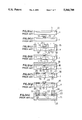
- FIG. 1 is a diagram showing a cross-sectional structure of a field effect transistor according to a first embodiment of the present invention
- FIGS. 2(a)-2(f) are diagrams showing a production method for producing the field effect transistor of FIG. 1;
- FIG. 3 is a diagram showing a cross-sectional structure of obtained by the production an FET according to a second embodiment of the present invention.
- FIGS. 4(a)-4(f) are diagrams showing a production method for producing the FET of FIG. 3;
- FIGS. 5(a)-5(g) are diagrams showing a production method of an FET according to a third embodiment of the present invention.
- FIGS. 6(a)-6(g) are diagrams showing a production method of an FET according to a fourth embodiment of the present invention.
- FIGS. 7(a)-7(b) are diagrams showing a prior art production method of an FET
- FIGS. 8(a)-8(b) are diagrams showing another prior art production method of an FET.
- FIGS. 9(a)-9(h) are diagrams showing another prior art production method of an FET.
- FIG. 1 and FIGS. 2(a)-2(f) respectively show a cross-sectional structure of an FET and a process flow of production method of an FET according to a first embodiment of the present invention.
- reference numeral 1 designates a GaAs substrate.
- Numeral 2 designates a refractory metal gate and numeral 3 designate an n-channel region produced at the surface of the substrate 1.
- Numerals 4 and 5 designate a source n + layer and a drain n + layer, respectively.
- Numeral 41 designates a source electrode and numeral 51 designates a drain electrode.
- Numeral 6 designates an insulating film.
- Numerals 7 and 7' designate photoresist patterns and reference numeral 8 designates an opening in the photoresist 7.
- Silicon ions are implanted by selective ion implantation into the GaAs substrate 1 at an energy of 10 to 50 keV and at a dose of 1 ⁇ 10 12 to 1 ⁇ 10 14 cm -2 .
- a film of AlN, SiN, SiON or SiO (not shown) is deposited on the substrate 1 to a thickness of approximately 100 to 1000 angstroms as a through-film for implantation and silicon ions are implanted through that film at an energy of 30 to 100 KeV and at a dose of approximately 1 ⁇ 10 12 to 1 ⁇ 10 14 cm -2 , thereby producing an n-channel region 3.
- a refractory metal such as tungsten silicide is deposited on the entire surface of the substrate and processed to a gate configuration 2 (FIG. 2(a)).
- SiON 6 first insulating film
- SiON 6 first insulating film
- the insulating film 6 is etched by a method such as plasma etching as shown in FIG. 2(d) and only the insulating film 6 at the source region is removed.
- the photoresist 7 is removed and the photoresist pattern 7' for determining the end of source region and the end of drain region is produced silicon ion implantation is carried out to produce the n + regions using this photoresist pattern as a mask at an energy of 20 to 200 keV and at a dose of 1 ⁇ 10 ⁇ 10 13 cm -2 or more.
- silicon ion implantation is carried out to produce the n + regions using this photoresist pattern as a mask at an energy of 20 to 200 keV and at a dose of 1 ⁇ 10 ⁇ 10 13 cm -2 or more.
- a drain n + layer 5 having a separation from the gate 2 corresponding approximately to the film thickness of the insulating film 6 and a source n + layer 4 close to the gate electrode 2 are produced self-alignedly at high precision. Further, the drain n + layer 5 is shallow and of low concentration and the source n + layer 4 is deep and of high concentration. Therefore, the drain breakdown voltage is enhanced and the short channel effect and the source resistance are reduced. Thus a high efficiency FET having a high transconductance gm can be produced with high controllability and high reproducibility.
- FIG. 3 shows a cross-sectional structure of an FET according to a second embodiment of the present invention and FIGS. 4(a)-4(f) show a production process of that structure.
- the same reference numerals designate the same portions as those in FIGS. 1 and 2.
- Reference numeral 9 designates an insulating film and reference numerals 9a and 9b designate side walls comprising the insulating film 9.
- a photoresist is applied so as to cover the surface of the substrate 1, the gate electrode 2, and the insulating film side walls 9a and 9b, and etching is carried out to produce an opening 8 at the photoresist 7 (FIG. 4(c)) so as to expose a portion of the surface of the side wall 9b at the source side and a portion of the substrate 1 at the source side region.
- the insulating film side wall 9b is etched and removed (FIG. 4(d)) using such as plasma etching, by the same process as that shown in FIG. 2(d).
- photoresist pattern 7' is produced and ion implantation for producing n + regions is carried out using the photoresist 7' as a mask, so that a drain n + layer 5 separated from the gate and a source n + layer 4 in contact with the gate are produced (FIG. 4(f)).
- This embodiment is different from the first embodiment described above in that the separation between the gate electrode 2 and the drain n + layer 5 is self-alignedly determined by the width of the insulating film side wall 9a.
- the insulating film 9b on the source n + region and the insulating film 9a on the drain n + region are produced with the gate electrode 2 therebetween, the insulating film 9b on the source n + region is easily and selectively removed with high controllability.
- the separation of the source n + layer and the drain n + layer from the gate electrode 2 can be set to desired values with high precision is obtained with high reproducibility and high controllability.
- the source n + layer 4 and drain n + layer 5 have the same concentrations and the same dopant depths in contrast to the above described embodiment. Whether the structure and the production method of the above described embodiment or those of this embodiment are to be adopted may be selected in accordance with the use of the element.
- a stopper that prevents removal of the insulating film just above the gate and the insulating. film above the drain n + layer is produced while the insulating film on the source n + layer is selectively removed, thereby enhancing the preference of etching. That is, different kinds of insulating films having different etching properties are inserted so that the source n + layer insulating film and the drain n + layer insulating film are not connected with each other as the same film.
- FIGS. 5(a)-5(g) show a production process of this third embodiment.
- a refractory gate is produced on the n-channel region 3 of GaAs substrate 1, an insulating film (first insulating film) 10 is deposited thereon and these are processed to a gate configuration in a two layer structure. Thereafter an insulating film (second insulating film) 6 having an etching property different from that of the first insulating film 10 is provided on the entire surface (FIG. 5(b)).
- the second insulating film 6 is etched back to expose the surface of the first insulating film 10 (FIG. 5(c)), a photoresist 11 is provided on the entire surface and an opening 8 which reaches the second insulating film 6 is produced at a portion of the photoresist 11 on the source n + region (FIG. 5(d)).
- the second insulating film 6 on the source n + region is selectively removed by etching using this photoresist pattern 11 as a mask.
- plasma etching (PE) using SF 6 for the selective removal of the first insulating film is preferable and it is possible for the second insulating film 6 to have a large selectivity relative to the first insulating film 10.
- the second insulating film 6 remaining on the drain n + region is etched and processed so as to remain only as a side wall at the gate electrode drain side. At this time, since the width of this side wall becomes the distance between the gate and the drain n + region, it should be previously produced at a design value.
- ion implantation for producing n + regions is carried over the entire surface of the substrate and a drain n + region 5 separated by a predetermined distance from the gate electrode 2 and a source n + region 4 in contact with the gate electrode 2 are produced self-alignedly with the gate electrode and the second insulating film side wall 6.
- a refractory gate 2 is produced at the surface of GaAs substrate 1 on which the n-channel region 3 is produced and the first insulating film 6 is deposited on the entire surface so as to cover the surface of the substrate 1 and the gate 2. Thereafter, the first insulating film 6 is etched back to expose the surface of the gate electrode 2 (FIG. 6(b)).
- a second insulating film 10 having a different etching property of from that of the first insulating film 6 is provided so as to cover the entire surface of the first insulating film 6 and the exposed gate electrode 2 (FIG. 6(c)).
- This insulating film 10 is processed so as to remain only at the surface of the gate electrode 2 and the surface of the first insulating film 6 on the drain n + region (FIG. 6(d)).
- a photoresist pattern 11 having an opening 8 at a portion on the source n + region is provided, and using the etching conditions described with respect to the process of FIG. 5(d) of the above described embodiment only the first insulating film 6 on the source n + region is selectively removed.
- the photoresist 11 is removed (FIG. 6(f))
- the second insulating film 10 is removed and thereafter the remaining first insulating film 6 is processed so as to remain only as a side wall of the gate electrode on the drain side.
- the ion implantation for producing n + layers is carried out using the gate electrode 2 and the side wall insulating film 6 as a mask.
- the drain n + region 5 is produced separated from the gate electrode by the width of the side wall and a source n + region 4 is produced adjacent to the gate electrode 2.
- a different kind of insulating film 10 that has a different etching property of is inserted in order that the insulating film 6 on the source n + layer and the insulating film 6 on the drain n + layer are not connected with each other as the same film.
- the insulating film 6 on the source n + layer and the insulating film 6 on the drain n + layer are separated and so selective removal of only the insulating film 6 on the source n + layer is reliably carried out.
- transistors in which respective layers are provided parallel to the substrate surface such an HEMT, MIS-like FET or Si MOSFET can be constructed with the same effects.
- GaAs is used for the substrate material 1, silicon or InP can be used therefor.
- a drain n + layer and a source n + layer are self-alignedly produced with a separation from the gate to drain length corresponding to the film thickness of the insulating film 6, by ion implantation using the insulating film 6 which is produced by high controllability etching, without using a mask produced by photolithography or without using diagonal ion implantation method.
- the drain and source are produced such that the former is shallow and of low concentration and the latter is deep and of high concentration. Therefore, a high efficiency FET having a high drain breakdown voltage, a reduced short channel effect, a small source resistance, and a high transconductance gm can be produced with high reproducibility and high controllability.
- the separation length between the drain n + layer and the gate is determined self-alignedly by the width of the side wall 9.
- the insulating film on the source n + layer and the insulating film on the drain n + layer are separated, the insulating film on the source n + layer can be reliably selectively removed.
- a drain n + layer is shallow and of low concentration compared with the source n + layer and only the drain n + layer is separated from the gate in an FET having an asymmetric gate, a high efficiency FET having a reduced short channel effect, reduced source resistance, high transconductance, and high drain breakdown voltage is obtained.
- drain n + layer is produced by the implantation through the insulating film and the source n + layer is produced either by implantation on a bare surface or by implantation through a film thinner than the implantation through film for producing the drain n + layer, only the drain n + layer is separated from the gate. Then, a good efficiency FET having reduced short channel effect, reduced source resistance, improved transconductance, and improved drain breakdown voltage is self-alignedly produced with high controllability and high reproducibility, without utilizing diagonal implantation which introduces an instability. This means that a high efficiency FET having stable characteristics from run to run is produced.
- the insulating film on the source n + layer can be reliably selectively removed, thereby resulting in high controllability and high reproducibility in the fabrication process.
Abstract
A field effect transistor having an asymmetric gate includes high dopant concentration source and drain regions. The drain region is shallower and of lower dopant concentration than the source region. The drain is spaced from the gate electrode. Therefore, an ideal FET having a reduced short channel effect and having a lower source resistance and high current drivability (gm) is obtained. When the drain region is produced by ion implantation through a film and the source region is produced by the implantation directly into the substrate, only the drain region is separated from the gate. When the insulating film on the source region is separated from the insulating film on the drain region, the insulating film on the source region is reliably selectively removed, whereby high controllability is obtained.
Description
This application is a division of application Ser. No. 07/881,291, filed May 11, 1992 now U.S. Pat. No. 5,296, which itself is a division of application Ser. No. 07/673,339, filed Mar. 22, 1991, now U.S. Pat. No. 5,153,683.
The present invention relates to a field effect transistor (hereinafter referred to as "FET") having an asymmetrical gate and a production method thereof.
FIGS. 7(a) and 7(b) show a prior art production method of a self-aligned gate FET recited in Electronics Information and Communication Engineer's Society of Japan, Electronic Device Research Institute report, ED86-9, pp. 23 to 28, "Optimization of MMIC GaAs Advanced SAINT Structure" (reference No. 1).
In FIGS. 7(a) and 7(b) reference numeral 1 designates a GaAs substrate. A p well 24 is produced in the substrate 1. N-channel region 3 is produced in the p well 24. N+ ion implanted regions 16 and 17 constitute a source and a drain region, respectively. Numeral 12 designates a through-film for implantation comprising SiN which functions as a mask for ion implantation. Numeral 23 designates a dummy gate comprising a T-shaped photoresist. Numeral 25 designates a SiO2 film. Numeral 26 designates a gate electrode. Numerals 61 and 71 designate a source and a drain electrode, respectively.
It is described in the reference No. 1 that an n+ ion implantation is carried out using the T-shaped photoresist as a mask (FIG. 7(a)), and further a pattern inversion is carried out and the gate electrode is produced by the lift-off method, resulting in a structure shown in FIG. 7(b).
However, in the FET produced in this way, because the source and drain regions are symmetrical with respect to the gate electrode 26, the interval between the source region 16 and the drain region 17 is reduced as is of the gate length. The substrate leakage current between source and drain increases, thereby causing the short channel effect. In addition, when the distance between the gate and source is shortened to reduce the source resistance, the distance between the gate and drain is also necessarily shortened and the gate drain breakdown voltage is reduced.
In order to reduce the short channel effect and increase the gate drain breakdown voltage, conventional methods of producing an FET having an asymmetrical gate described in the following, is proposed.
One of them, which is also recited in the reference No. 1, will be described with reference to FIGS. 8(a) and 8(b). In FIGS. 8(a) and 8(b) the same reference numerals designate the same parts as in FIGS. 7(a) and 7(b). It is described in the reference No. 1 that the device is produced as follows:
After p well 24 and n type layer 3 are produced by ion implantation, a plasma CVD SiN film 12 is deposited, and a T-shaped dummy gate 23 is produced thereon. Using this dummy gate 23 as a mask, n+ ion implantation is carried out (FIG. 8(a)). The angle of ion implantation is determined such that the distance between the gate electrode and the end of the n+ layer at the drain side (Lgd) is larger than the distance between the gate electrode and the source side (Lsg). Next, using an inverted pattern of dummy gate 23 as a mask, a Schottky Junction part is opened and Mo/Au is deposited by DC sputtering. Then, by flattening the Au using diagonal direction ion milling, a gate electrode 26 is produced only on the Schottky junction part and finally ohmic electrodes 61, 71 are produced by lift-off and sintered, thereby resulting in a device of FIG. 8(b).
The n+ implanted layers which are produced by the diagonal direction ion implantation using the T-shaped gate electrode which is symmetric with respect to the source and drain as a mask results in a difference between the gate-source distance Lsg and the gate-drain distance Lgd. This makes it possible to reduce the source resistance and to enhance the gate drain breakdown voltage at the same time. Furthermore, this enables a long distance between the source and the drain region, resulting in reduction in the short channel effect.
FIGS 9(a)-9(h) show another prior art method of producing FET having an asymmetric self-aligned gate, which is recited in IEEE Transactions on Electron Devices, Vol. 35, No. 5, May 1988, pp. 615 to 622, "A New Refractory Self-Aligned Gate Technology for GaAs Microwave Power FET's and MMIC's" (reference. No. 2).
The production method will be described.
As shown in FIG. 9(a), a SiON film 12 is produced as through-film for implantation on a GaAs substrate 1, and thereafter, an active channel region 3 of FET is produced by selective ion implantation of silicon ions. Thereafter, the SiON film 12 is removed, a TiWN film is produced on the entire surface by sputtering, an etching mask comprising Ni 14 is produced at a gate electrode production region and the TiWN layer is processed so as to have a gate configuration 13 by reactive ion etching (FIG. 9(b)).
Next, a photoresist pattern 15 of a configuration that covers the drain side of the gate electrode 13 is produced as a mask for n+ ion implantation, and n+ ion implantation is carried out using the same as a mask to produce asymmetrical n+ ion implanted regions 16 and 17 among which the drain region is located farther from the gate electrode 13 than the source region (FIG. 9(c)).
Next, the photoresist 15 and Ni film 14 are removed, a SiON film 18 is provided on the entire surface of the substrate as a protection film which functions as an anneal cap, and then an annealing is carried out to activate the implanted ions in the regions 16 and 17 (FIG. 9(d)). Thereafter, a flattening photoresist 19 is provided on the entire surface of substrate (FIG. 9(e)), gate 13 is exposed by etching back, and ohmic metals 20 and 21 which are to be a source electrode and a drain electrode are produced by burying metal (FIG. 9(f)).
Next, a low resistance metal 22 of Ti/Au is produced on the gate electrode 13 by evaporation and lift-off (FIG. 9(g)), and thereafter a SiN film 27 is produced on the surface and Au electrodes 28 are produced on the ohmic electrodes 20 and 21 via TiWN layers 29. Further, an opening is provided at a part of the source electrode 20 from the rear surface of the substrate 1 and Au electrode 28 is plated on the rear surface covering the side wall of the opening and the entire rear surface of substrate, thereby completing the device (FIG. 9(h)).
In this production method, the photoresist pattern 15 is produced only covering the drain side of the gate electrode 13, n+ ion implantation of so that n+ layer producing ions are not implanted into the vicinity of the gate electrode at the drain side. Thus an asymmetrical gate FET is produced.
In the prior art production method shown in FIGS. 8(a) and 8(b) the asymmetry of the production position of n+ layer with respect to the gate is realized by a diagonal implantation, and the angle of the diagonal implantation varies depending on position in the GaAs wafer surface. The position of the end portion of n+ layer is likely to vary depending on the configuration of T-shaped gate which functions as an implantation mask. That is, the position where the n+ layer is produced is likely to be affected by variations in the configuration of T-shaped gate cause variations in characteristics.
In the prior art production method shown in FIGS. 9(a)-9(h), the photoresist mask which is produced at the drain side of the gate is position determined only by photolithography and therefore the positioning of the photoresist mask is quite unstable. That is, the precision of the photoresist mask largely depends on the performance of the photolithography apparatus and it may possibly vary from run to run. Therefore, an asymmetrical gate FET having a stable gate drain distance and a gate source distance as designed can not be produced with high reproducibility.
The present invention is directed to solving the abovedescribed problems and has for its object to provide a field effect transistor having an asymmetric gate that is produced by asymmetric implantation self-alignedly and having a gate drain distance and a gate source distance with high precision and reproducibility.
Another object of the present invention is provide a production method for such an FET.
Other objects and advantages of the present invention will become apparent from the detailed description given hereinafter; it should be understood, however, that the detailed description and specific embodiment are given by way of illustration only, since various changes and modifications within the spirit and scope of the invention will become apparent to those skilled in the art from this detailed description.
In accordance with a first aspect of the present invention, in a field effect transistor having an asymmetric gate structure, the drain layer is made shallower and of lower concentration than the source layer and only the drain layer is separated from the gate.
In accordance with a second aspect of the present invention, an insulating film is provided covering the substrate on which a gate electrode is produced, a photoresist pattern having an opening only at the source region is produced on this insulating film, the insulating film on the source region is selectively removed using the photoresist as a mask, and thereafter, using the insulating film on the gate electrode and the drain region as a mask, ion implantation is carried out, thereby producing source and drain layers.
In accordance with a third aspect of the present invention, side walls comprising an insulating film are produced at both sides of the gate electrode, a photoresist pattern having an opening only at the source region is produced, and the side wall at the side of the source region is selectively removed using a photoresist pattern as a mask, and ion implantation is carried out using the gate electrode and the side wall remaining at the side of drain region as mask, thereby producing source and drain layers.
In accordance with a fourth aspect of the present invention, a first insulating film is produced on the gate electrode, a second insulating film is provided to covering the entire surface of the substrate, this second insulating film is etched back to expose the first insulating film, a photoresist pattern having an opening only at a portion of the source region is provided, the second insulating film on the source region is selectively removed using the photoresist pattern as a mask, and thereafter the second insulating film on the drain region is processed so as to remain at the side of the gate electrode by etching and to become a side wall, ion implantation is carried out using the gate electrode and the second insulating film of the side wall part as a mask, and thus source and drain layers are produced.
In accordance with a fifth aspect of the present invention, a first insulating film is provided to covering the surface of substrate where a gate electrode is produced and etched back to expose the gate electrode; a second insulating film is produced so as to cover the gate electrode and the first insulating film at the drain side, a photoresist pattern having an opening only at a portion on the first insulating film on the source region is provided, the first insulating film on the source region is selectively removed using the photoresist pattern as a mask, and thereafter the first insulating film on the drain region is etched so as to remain at the side of the gate electrode and to become a side wall, and ion implantation is carried out using the gate electrode and the first insulating film at the side wall part as a mask to produce source and drain layers.
In accordance with the first aspect of the present invention, an ideal FET having a reduced short channel effect, a small source resistance and high current drivability (gm) can be obtained.
In accordance with the second aspect of the present invention, since the drain layer is formed by implantation through the other insulating film and the source layer is formed by implantation in the bare surface or through a film which is thinner than the through film for producing the drain layer, the drain layer is produced self-alignedly, has a separation from the gate which is almost determined by the thickness of the through film and is shallower and of lower dopant concentration than the source layer. Furthermore, the source layer is located closer to the gate than the drain layer is deeper and of a higher concentration than the drain layer, thereby realizing an FET which has a reduced short channel effect, a small source resistance and a high current drivability (gm) at a high controllability.
In accordance with the third aspect of the present invention, since only the drain layer is separated from the gate by a side wall insulating film only at the drain side end of the gate and the source layer is closer to the gate than the drain layer, the drain layer and the source layer are produced at the same depth and of the same concentration. Also in this case, an FET having a reduced short channel effect, a small source resistance and a high current drivability (gm) is obtained.
In accordance with the fourth aspect of the present invention, since a first insulating film comprising a material different from that of the second insulating film on the source and drain region is provided only direct by above the gate electrode and the second insulating film on the source region is selectively removed, the selective removal of the second insulating film on the source region can be reliably carried out for asymmetrical ion implantation for producing the drain and the source layers.
In accordance with the fifth aspect of the present invention, since a second insulating film comprising a material different from the first insulating film on the source region is provided in contact with the first insulating film on the gate electrode and on the drain region, the selective removal of the first insulating film on the source region can be reliably carried out.
FIG. 1 is a diagram showing a cross-sectional structure of a field effect transistor according to a first embodiment of the present invention;
FIGS. 2(a)-2(f) are diagrams showing a production method for producing the field effect transistor of FIG. 1;
FIG. 3 is a diagram showing a cross-sectional structure of obtained by the production an FET according to a second embodiment of the present invention;
FIGS. 4(a)-4(f) are diagrams showing a production method for producing the FET of FIG. 3;
FIGS. 5(a)-5(g) are diagrams showing a production method of an FET according to a third embodiment of the present invention;
FIGS. 6(a)-6(g) are diagrams showing a production method of an FET according to a fourth embodiment of the present invention;
FIGS. 7(a)-7(b) are diagrams showing a prior art production method of an FET;
FIGS. 8(a)-8(b) are diagrams showing another prior art production method of an FET; and
FIGS. 9(a)-9(h) are diagrams showing another prior art production method of an FET.
An embodiment of the present invention will be described in detail with reference to the drawings.
FIG. 1 and FIGS. 2(a)-2(f) respectively show a cross-sectional structure of an FET and a process flow of production method of an FET according to a first embodiment of the present invention. In these figures, reference numeral 1 designates a GaAs substrate. Numeral 2 designates a refractory metal gate and numeral 3 designate an n-channel region produced at the surface of the substrate 1. Numerals 4 and 5 designate a source n+ layer and a drain n+ layer, respectively. Numeral 41 designates a source electrode and numeral 51 designates a drain electrode. Numeral 6 designates an insulating film. Numerals 7 and 7' designate photoresist patterns and reference numeral 8 designates an opening in the photoresist 7.
A description is given of the production method.
Silicon ions are implanted by selective ion implantation into the GaAs substrate 1 at an energy of 10 to 50 keV and at a dose of 1×10¹² to 1×1014 cm-2. Thereafter a film of AlN, SiN, SiON or SiO (not shown) is deposited on the substrate 1 to a thickness of approximately 100 to 1000 angstroms as a through-film for implantation and silicon ions are implanted through that film at an energy of 30 to 100 KeV and at a dose of approximately 1×10¹² to 1×1014 cm-2, thereby producing an n-channel region 3. Thereafter, a refractory metal such as tungsten silicide is deposited on the entire surface of the substrate and processed to a gate configuration 2 (FIG. 2(a)).
Next, SiON 6 (first insulating film) is deposited on the surface of the substrate 1 and the refractory gate 2 to a film thickness of approximately 1000 to 10000 angstroms, and a photoresist pattern 7 having an opening 8 at a part of source region is produced thereon (FIG. 2(b)). FIG. 2(c) shows a view from just above the substrate.
Next, the insulating film 6 is etched by a method such as plasma etching as shown in FIG. 2(d) and only the insulating film 6 at the source region is removed.
Thereafter, as shown in FIG. 2(e), the photoresist 7 is removed and the photoresist pattern 7' for determining the end of source region and the end of drain region is produced silicon ion implantation is carried out to produce the n+ regions using this photoresist pattern as a mask at an energy of 20 to 200 keV and at a dose of 1˜10×1013 cm-2 or more. Thus, a shallow and low concentration drain n+ layer 5 which is separated from the gate and a deep and high concentration source n+ layer 4 in contact with the gate are produced.
Thereafter, the photoresist 7' and the insulating film 6 are removed and the source electrode 41 and the drain electrode 51 are produced to complete an element of FIG. 1.
In this embodiment, without using photolithographic mask alignment for producing an ion implantation mask, a drain n+ layer 5 having a separation from the gate 2 corresponding approximately to the film thickness of the insulating film 6 and a source n+ layer 4 close to the gate electrode 2 are produced self-alignedly at high precision. Further, the drain n+ layer 5 is shallow and of low concentration and the source n+ layer 4 is deep and of high concentration. Therefore, the drain breakdown voltage is enhanced and the short channel effect and the source resistance are reduced. Thus a high efficiency FET having a high transconductance gm can be produced with high controllability and high reproducibility.
FIG. 3 shows a cross-sectional structure of an FET according to a second embodiment of the present invention and FIGS. 4(a)-4(f) show a production process of that structure. In these figures, the same reference numerals designate the same portions as those in FIGS. 1 and 2. Reference numeral 9 designates an insulating film and reference numerals 9a and 9b designate side walls comprising the insulating film 9.
A description is given of a production method.
The processes that produce an n-channel region 3 by selective ion implantation on the GaAs substrate 1, a refractory metal such as tungsten silicide on the entire surface of the substrate and a gate configuration 2 are the same as those shown in FIG. 2(a). In this embodiment, subsequently an insulating film 9 is deposited on the surface of substrate 1 and the surface of gate electrode 2 to cover the same (FIG. 4(a)). Thereafter, the insulating film 9 is etched leaving side walls 9a and 9b at the both sides of the gate electrode 2 (FIG. 4(b)).
Then, a photoresist is applied so as to cover the surface of the substrate 1, the gate electrode 2, and the insulating film side walls 9a and 9b, and etching is carried out to produce an opening 8 at the photoresist 7 (FIG. 4(c)) so as to expose a portion of the surface of the side wall 9b at the source side and a portion of the substrate 1 at the source side region.
Next, the insulating film side wall 9b is etched and removed (FIG. 4(d)) using such as plasma etching, by the same process as that shown in FIG. 2(d).
Thereafter, as shown in FIG. 4(e), after the photoresist 7 is removed, photoresist pattern 7' is produced and ion implantation for producing n+ regions is carried out using the photoresist 7' as a mask, so that a drain n+ layer 5 separated from the gate and a source n+ layer 4 in contact with the gate are produced (FIG. 4(f)).
Thereafter, after the photoresist 7' is removed, a source electrode 41 and a drain electrode 51 are produced, thereby completing the element of FIG. 3.
This embodiment is different from the first embodiment described above in that the separation between the gate electrode 2 and the drain n+ layer 5 is self-alignedly determined by the width of the insulating film side wall 9a. In this embodiment, since the insulating film 9b on the source n+ region and the insulating film 9a on the drain n+ region are produced with the gate electrode 2 therebetween, the insulating film 9b on the source n+ region is easily and selectively removed with high controllability. Furthermore, in this embodiment, since no variation in position of n+ layer edge is caused by an unstable implantation such as diagonal ion implantation or by an implantation mask produced by photolitography, the separation of the source n+ layer and the drain n+ layer from the gate electrode 2 can be set to desired values with high precision is obtained with high reproducibility and high controllability. Furthermore, in this production method, the source n+ layer 4 and drain n+ layer 5 have the same concentrations and the same dopant depths in contrast to the above described embodiment. Whether the structure and the production method of the above described embodiment or those of this embodiment are to be adopted may be selected in accordance with the use of the element.
Next, third and fourth embodiments of the present invention which are alternatives of the first and second embodiments will be described.
In these embodiments a stopper that prevents removal of the insulating film just above the gate and the insulating. film above the drain n+ layer is produced while the insulating film on the source n+ layer is selectively removed, thereby enhancing the preference of etching. That is, different kinds of insulating films having different etching properties are inserted so that the source n+ layer insulating film and the drain n+ layer insulating film are not connected with each other as the same film.
FIGS. 5(a)-5(g) show a production process of this third embodiment.
As shown in FIG. 5(a), a refractory gate is produced on the n-channel region 3 of GaAs substrate 1, an insulating film (first insulating film) 10 is deposited thereon and these are processed to a gate configuration in a two layer structure. Thereafter an insulating film (second insulating film) 6 having an etching property different from that of the first insulating film 10 is provided on the entire surface (FIG. 5(b)).
Thereafter, the second insulating film 6 is etched back to expose the surface of the first insulating film 10 (FIG. 5(c)), a photoresist 11 is provided on the entire surface and an opening 8 which reaches the second insulating film 6 is produced at a portion of the photoresist 11 on the source n+ region (FIG. 5(d)).
Thereafter, the second insulating film 6 on the source n+ region is selectively removed by etching using this photoresist pattern 11 as a mask. Here, in a case where SiN is used for the second insulating film 6 and SiO2 or SiO is used for the first insulating film 10, plasma etching (PE) using SF6 for the selective removal of the first insulating film is preferable and it is possible for the second insulating film 6 to have a large selectivity relative to the first insulating film 10. Furthermore, when SiO2 or SiO are used for the second insulating film 6 and SiN is used for the first insulating film 10, it is quite effective to utilize reactive ion etching using CHF3 +C2 H6 for the selective removal of the second insulating film 6.
Next, as shown in FIG. 5(e), after the photoresist 11 is removed, the second insulating film 6 remaining on the drain n+ region is etched and processed so as to remain only as a side wall at the gate electrode drain side. At this time, since the width of this side wall becomes the distance between the gate and the drain n+ region, it should be previously produced at a design value.
Next, as shown in FIG. 5(g), ion implantation for producing n+ regions is carried over the entire surface of the substrate and a drain n+ region 5 separated by a predetermined distance from the gate electrode 2 and a source n+ region 4 in contact with the gate electrode 2 are produced self-alignedly with the gate electrode and the second insulating film side wall 6.
A production process flow of the fourth embodiment will be described with reference to FIGS. 6(a)-6(g).
As shown in FIG. 6(a), a refractory gate 2 is produced at the surface of GaAs substrate 1 on which the n-channel region 3 is produced and the first insulating film 6 is deposited on the entire surface so as to cover the surface of the substrate 1 and the gate 2. Thereafter, the first insulating film 6 is etched back to expose the surface of the gate electrode 2 (FIG. 6(b)).
Thereafter, a second insulating film 10 having a different etching property of from that of the first insulating film 6 is provided so as to cover the entire surface of the first insulating film 6 and the exposed gate electrode 2 (FIG. 6(c)). This insulating film 10 is processed so as to remain only at the surface of the gate electrode 2 and the surface of the first insulating film 6 on the drain n+ region (FIG. 6(d)).
Next, as shown in FIG. 6(e), a photoresist pattern 11 having an opening 8 at a portion on the source n+ region is provided, and using the etching conditions described with respect to the process of FIG. 5(d) of the above described embodiment only the first insulating film 6 on the source n+ region is selectively removed. After the photoresist 11 is removed (FIG. 6(f)), the second insulating film 10 is removed and thereafter the remaining first insulating film 6 is processed so as to remain only as a side wall of the gate electrode on the drain side. The ion implantation for producing n+ layers is carried out using the gate electrode 2 and the side wall insulating film 6 as a mask. The drain n+ region 5 is produced separated from the gate electrode by the width of the side wall and a source n+ region 4 is produced adjacent to the gate electrode 2.
In the above described third and fourth embodiments, a different kind of insulating film 10 that has a different etching property of is inserted in order that the insulating film 6 on the source n+ layer and the insulating film 6 on the drain n+ layer are not connected with each other as the same film. In this production method, the insulating film 6 on the source n+ layer and the insulating film 6 on the drain n+ layer are separated and so selective removal of only the insulating film 6 on the source n+ layer is reliably carried out.
In the above illustrated embodiments, only GaAs MESFETs are described, but transistors in which respective layers are provided parallel to the substrate surface such an HEMT, MIS-like FET or Si MOSFET can be constructed with the same effects.
While in the above illustrated embodiments, GaAs is used for the substrate material 1, silicon or InP can be used therefor.
In summary, in the above described first embodiment, a drain n+ layer and a source n+ layer are self-alignedly produced with a separation from the gate to drain length corresponding to the film thickness of the insulating film 6, by ion implantation using the insulating film 6 which is produced by high controllability etching, without using a mask produced by photolithography or without using diagonal ion implantation method. The drain and source are produced such that the former is shallow and of low concentration and the latter is deep and of high concentration. Therefore, a high efficiency FET having a high drain breakdown voltage, a reduced short channel effect, a small source resistance, and a high transconductance gm can be produced with high reproducibility and high controllability. In the second embodiment of the present invention, while the same effects as the first embodiment are obtained, the separation length between the drain n+ layer and the gate is determined self-alignedly by the width of the side wall 9. In addition, in the third and fourth embodiments, since the insulating film on the source n+ layer and the insulating film on the drain n+ layer are separated, the insulating film on the source n+ layer can be reliably selectively removed.
As is evident from the foregoing description, in accordance with present invention, since a drain n+ layer is shallow and of low concentration compared with the source n+ layer and only the drain n+ layer is separated from the gate in an FET having an asymmetric gate, a high efficiency FET having a reduced short channel effect, reduced source resistance, high transconductance, and high drain breakdown voltage is obtained.
In addition, when the drain n+ layer is produced by the implantation through the insulating film and the source n+ layer is produced either by implantation on a bare surface or by implantation through a film thinner than the implantation through film for producing the drain n+ layer, only the drain n+ layer is separated from the gate. Then, a good efficiency FET having reduced short channel effect, reduced source resistance, improved transconductance, and improved drain breakdown voltage is self-alignedly produced with high controllability and high reproducibility, without utilizing diagonal implantation which introduces an instability. This means that a high efficiency FET having stable characteristics from run to run is produced. In addition, when a structure in which the insulating film on the source n+ layer is separated from the insulating film on the drain n+ layer is obtained in the fabrication process, the insulating film on the source n+ layer can be reliably selectively removed, thereby resulting in high controllability and high reproducibility in the fabrication process.
Claims (1)
1. A production method of a field effect transistor comprising:
producing a gate electrode on a substrate;
depositing a first insulating film covering said gate electrode and said substrate;
etching said first insulating film to expose said gate electrode;
depositing a second insulating layer comprising a material different from that of said first insulating film on said first insulating film and removing part of said second insulating layer, leaving a second insulating layer only at a first side of said gate electrode and on said gate electrode;
depositing a photoresist layer and patterning said photoresist layer to leave a photoresist film on said first and second insulating films, said photoresist film having an opening at and exposing part of said first insulating film at a second side of said gate electrode on the opposite side of said gate electrode from the first side of said gate electrode and selectively removing said first insulating film at the second side of said gate electrode using said photoresist film as a mask;
removing said photoresist film and said second insulating film;
etching said first insulating film remaining on said substrate to leave a side wall of said first insulating film at the first side of said gate electrode; and
implanting ions using said gate electrode and said side wall of said first insulating film as masks to produce source and drain regions in said substrate.
Priority Applications (1)
| Application Number | Priority Date | Filing Date | Title |
|---|---|---|---|
| US08/074,564 US5344788A (en) | 1990-04-19 | 1993-06-10 | Method of making field effect transistor |
Applications Claiming Priority (5)
| Application Number | Priority Date | Filing Date | Title |
|---|---|---|---|
| JP2-104038 | 1990-04-19 | ||
| JP2104038A JP2786307B2 (en) | 1990-04-19 | 1990-04-19 | Field effect transistor and method of manufacturing the same |
| US07/673,339 US5153683A (en) | 1990-04-19 | 1991-03-22 | Field effect transistor |
| US07/881,291 US5296398A (en) | 1990-04-19 | 1992-05-11 | Method of making field effect transistor |
| US08/074,564 US5344788A (en) | 1990-04-19 | 1993-06-10 | Method of making field effect transistor |
Related Parent Applications (1)
| Application Number | Title | Priority Date | Filing Date |
|---|---|---|---|
| US07/881,291 Division US5296398A (en) | 1990-04-19 | 1992-05-11 | Method of making field effect transistor |
Publications (1)
| Publication Number | Publication Date |
|---|---|
| US5344788A true US5344788A (en) | 1994-09-06 |
Family
ID=14370057
Family Applications (4)
| Application Number | Title | Priority Date | Filing Date |
|---|---|---|---|
| US07/673,339 Expired - Fee Related US5153683A (en) | 1990-04-19 | 1991-03-22 | Field effect transistor |
| US07/881,291 Expired - Fee Related US5296398A (en) | 1990-04-19 | 1992-05-11 | Method of making field effect transistor |
| US08/074,564 Expired - Fee Related US5344788A (en) | 1990-04-19 | 1993-06-10 | Method of making field effect transistor |
| US08/074,355 Expired - Fee Related US5510280A (en) | 1990-04-19 | 1993-06-10 | Method of making an asymmetrical MESFET having a single sidewall spacer |
Family Applications Before (2)
| Application Number | Title | Priority Date | Filing Date |
|---|---|---|---|
| US07/673,339 Expired - Fee Related US5153683A (en) | 1990-04-19 | 1991-03-22 | Field effect transistor |
| US07/881,291 Expired - Fee Related US5296398A (en) | 1990-04-19 | 1992-05-11 | Method of making field effect transistor |
Family Applications After (1)
| Application Number | Title | Priority Date | Filing Date |
|---|---|---|---|
| US08/074,355 Expired - Fee Related US5510280A (en) | 1990-04-19 | 1993-06-10 | Method of making an asymmetrical MESFET having a single sidewall spacer |
Country Status (4)
| Country | Link |
|---|---|
| US (4) | US5153683A (en) |
| JP (1) | JP2786307B2 (en) |
| FR (2) | FR2661278A1 (en) |
| GB (1) | GB2243950B (en) |
Cited By (5)
| Publication number | Priority date | Publication date | Assignee | Title |
|---|---|---|---|---|
| US5462884A (en) * | 1991-10-14 | 1995-10-31 | Mitsubishi Denki Kabushiki Kaisha | Method of making field effect transistor with T-shaped gate electrode |
| US5536666A (en) * | 1994-06-03 | 1996-07-16 | Itt Corporation | Method for fabricating a planar ion-implanted GaAs MESFET with improved open-channel burnout characteristics |
| US5681769A (en) * | 1994-09-06 | 1997-10-28 | Integrated Device Technology, Inc. | Method of fabricating a high capacitance insulated-gate field effect transistor |
| US5705439A (en) * | 1996-04-22 | 1998-01-06 | Taiwan Semiconductor Manufacturing Company Ltd. | Method to make an asymmetrical LDD structure for deep sub-micron MOSFETS |
| US20050251083A1 (en) * | 2004-02-12 | 2005-11-10 | Victoria Carr-Brendel | Biointerface with macro-and micro-architecture |
Families Citing this family (42)
| Publication number | Priority date | Publication date | Assignee | Title |
|---|---|---|---|---|
| FR2686734B1 (en) * | 1992-01-24 | 1994-03-11 | Thomson Composants Microondes | PROCESS FOR PRODUCING A TRANSISTOR. |
| JP3221766B2 (en) * | 1993-04-23 | 2001-10-22 | 三菱電機株式会社 | Method for manufacturing field effect transistor |
| KR960014718B1 (en) * | 1993-05-14 | 1996-10-19 | Lg Semicon Co Ltd | Method of manufacturing transistor |
| US5484740A (en) * | 1994-06-06 | 1996-01-16 | Motorola, Inc. | Method of manufacturing a III-V semiconductor gate structure |
| KR0137693B1 (en) * | 1994-12-31 | 1998-06-15 | 김주용 | Self boothstrap device |
| US5935867A (en) * | 1995-06-07 | 1999-08-10 | Advanced Micro Devices, Inc. | Shallow drain extension formation by angled implantation |
| KR0161201B1 (en) * | 1995-10-23 | 1998-12-01 | 양승택 | Production method for ion-implanted mosfet comprising self-aligned lightly doped drain structure and t-gat |
| US5874340A (en) * | 1996-07-17 | 1999-02-23 | Advanced Micro Devices, Inc. | Method for fabrication of a non-symmetrical transistor with sequentially formed gate electrode sidewalls |
| US5672531A (en) * | 1996-07-17 | 1997-09-30 | Advanced Micro Devices, Inc. | Method for fabrication of a non-symmetrical transistor |
| US5648286A (en) * | 1996-09-03 | 1997-07-15 | Advanced Micro Devices, Inc. | Method of making asymmetrical transistor with lightly doped drain region, heavily doped source and drain regions, and ultra-heavily doped source region |
| US5877050A (en) * | 1996-09-03 | 1999-03-02 | Advanced Micro Devices, Inc. | Method of making N-channel and P-channel devices using two tube anneals and two rapid thermal anneals |
| US5677224A (en) | 1996-09-03 | 1997-10-14 | Advanced Micro Devices, Inc. | Method of making asymmetrical N-channel and P-channel devices |
| US6051471A (en) * | 1996-09-03 | 2000-04-18 | Advanced Micro Devices, Inc. | Method for making asymmetrical N-channel and symmetrical P-channel devices |
| US5985724A (en) * | 1996-10-01 | 1999-11-16 | Advanced Micro Devices, Inc. | Method for forming asymmetrical p-channel transistor having nitrided oxide patterned to selectively form a sidewall spacer |
| US5893739A (en) * | 1996-10-01 | 1999-04-13 | Advanced Micro Devices, Inc. | Asymmetrical P-channel transistor having a boron migration barrier and a selectively formed sidewall spacer |
| US5930592A (en) * | 1996-10-01 | 1999-07-27 | Advanced Micro Devices, Inc. | Asymmetrical n-channel transistor having LDD implant only in the drain region |
| US5909622A (en) * | 1996-10-01 | 1999-06-01 | Advanced Micro Devices, Inc. | Asymmetrical p-channel transistor formed by nitrided oxide and large tilt angle LDD implant |
| US5783458A (en) * | 1996-10-01 | 1998-07-21 | Advanced Micro Devices, Inc. | Asymmetrical p-channel transistor having nitrided oxide patterned to allow select formation of a grown sidewall spacer |
| US6027978A (en) * | 1997-01-28 | 2000-02-22 | Advanced Micro Devices, Inc. | Method of making an IGFET with a non-uniform lateral doping profile in the channel region |
| TW417256B (en) | 1997-01-31 | 2001-01-01 | Seiko Epson Corp | Semiconductor MOS device and its manufacturing method |
| US5923982A (en) * | 1997-04-21 | 1999-07-13 | Advanced Micro Devices, Inc. | Method of making asymmetrical transistor with lightly and heavily doped drain regions and ultra-heavily doped source region using two source/drain implant steps |
| US5963809A (en) * | 1997-06-26 | 1999-10-05 | Advanced Micro Devices, Inc. | Asymmetrical MOSFET with gate pattern after source/drain formation |
| US6004849A (en) * | 1997-08-15 | 1999-12-21 | Advanced Micro Devices, Inc. | Method of making an asymmetrical IGFET with a silicide contact on the drain without a silicide contact on the source |
| US5904529A (en) * | 1997-08-25 | 1999-05-18 | Advanced Micro Devices, Inc. | Method of making an asymmetrical IGFET and providing a field dielectric between active regions of a semiconductor substrate |
| US6096588A (en) * | 1997-11-01 | 2000-08-01 | Advanced Micro Devices, Inc. | Method of making transistor with selectively doped channel region for threshold voltage control |
| US6146952A (en) * | 1998-10-01 | 2000-11-14 | Advanced Micro Devices | Semiconductor device having self-aligned asymmetric source/drain regions and method of fabrication thereof |
| US6864131B2 (en) * | 1999-06-02 | 2005-03-08 | Arizona State University | Complementary Schottky junction transistors and methods of forming the same |
| US7589007B2 (en) * | 1999-06-02 | 2009-09-15 | Arizona Board Of Regents For And On Behalf Of Arizona State University | MESFETs integrated with MOSFETs on common substrate and methods of forming the same |
| US6153534A (en) * | 1999-07-27 | 2000-11-28 | Advanced Micro Devices, Inc. | Method for fabricating a dual material gate of a short channel field effect transistor |
| US6479843B2 (en) * | 2000-04-27 | 2002-11-12 | Motorola, Inc. | Single supply HFET with temperature compensation |
| DE10237508A1 (en) * | 2002-08-16 | 2004-03-11 | Infineon Technologies Ag | Process for forming a masking layer on a substrate |
| US20040087094A1 (en) * | 2002-10-30 | 2004-05-06 | Advanced Micro Devices, Inc. | Semiconductor component and method of manufacture |
| US6833307B1 (en) | 2002-10-30 | 2004-12-21 | Advanced Micro Devices, Inc. | Method for manufacturing a semiconductor component having an early halo implant |
| US7208383B1 (en) | 2002-10-30 | 2007-04-24 | Advanced Micro Devices, Inc. | Method of manufacturing a semiconductor component |
| US6794256B1 (en) * | 2003-08-04 | 2004-09-21 | Advanced Micro Devices Inc. | Method for asymmetric spacer formation |
| US6967363B1 (en) * | 2003-10-01 | 2005-11-22 | Advanced Micro Devices, Inc. | Lateral diode with multiple spacers |
| US20080191276A1 (en) * | 2007-02-08 | 2008-08-14 | Taiwan Semiconductor Manufacturing Co., Ltd. | Semiconductor devices and fabrication methods thereof |
| JP5200399B2 (en) * | 2007-03-26 | 2013-06-05 | 富士通セミコンダクター株式会社 | Manufacturing method of MOS transistor |
| WO2011030782A1 (en) * | 2009-09-09 | 2011-03-17 | 学校法人神奈川大学 | Method for forming a semiconductor element structure and semiconductor element |
| RU2641617C1 (en) * | 2016-10-07 | 2018-01-18 | Федеральное государственное бюджетное образовательное учреждение высшего образования "Чеченский государственный университет" | Method of manufacturing semiconductor device |
| US10741644B2 (en) * | 2016-11-22 | 2020-08-11 | Delta Electronics, Inc. | Semiconductor devices with via structure and package structures comprising the same |
| WO2018125074A1 (en) * | 2016-12-28 | 2018-07-05 | Intel Corporation | Asymmetric transistors and related devices and methods |
Citations (21)
| Publication number | Priority date | Publication date | Assignee | Title |
|---|---|---|---|---|
| GB402296A (en) * | 1931-11-07 | 1933-11-30 | H Th Boehme Ag | Improvements in or relating to dispersions or plastic preparations |
| US4318216A (en) * | 1978-11-13 | 1982-03-09 | Rca Corporation | Extended drain self-aligned silicon gate MOSFET |
| EP0110320A1 (en) * | 1982-11-27 | 1984-06-13 | Nissan Motor Co., Ltd. | A MOS transistor |
| EP0152615A2 (en) * | 1983-12-26 | 1985-08-28 | Kabushiki Kaisha Toshiba | Semiconductor device and a method of manufacturing the same |
| EP0160255A2 (en) * | 1984-04-30 | 1985-11-06 | General Electric Company | Field effect transistor device and method of making same |
| EP0177129A1 (en) * | 1984-09-29 | 1986-04-09 | Kabushiki Kaisha Toshiba | Method of manufacturing GaAs field effect transistor |
| JPS63107071A (en) * | 1986-10-23 | 1988-05-12 | Nec Corp | Manufacture of field effect transistor |
| JPS63280462A (en) * | 1987-05-12 | 1988-11-17 | Sharp Corp | Manufacture of field-effect transistor |
| EP0306039A2 (en) * | 1987-09-03 | 1989-03-08 | Kabushiki Kaisha Toshiba | Semiconductor device |
| US4859618A (en) * | 1986-11-20 | 1989-08-22 | Sumitomo Electric Industries, Ltd. | Method of producing the gate electrode of a field effect transistor |
| JPH0240924A (en) * | 1988-07-30 | 1990-02-09 | Nec Corp | Manufacture of semiconductor device |
| JPH0276236A (en) * | 1988-09-12 | 1990-03-15 | Oki Electric Ind Co Ltd | Manufacture of semiconductor device |
| FR2639762A1 (en) * | 1988-11-29 | 1990-06-01 | Mitsubishi Electric Corp | PROCESS FOR PRODUCING ASYMMETRIC FIELD TRANSISTORS AND TRANSISTORS THEREOF |
| US4956308A (en) * | 1987-01-20 | 1990-09-11 | Itt Corporation | Method of making self-aligned field-effect transistor |
| US4962054A (en) * | 1988-04-11 | 1990-10-09 | Sumitomo Electric Industries, Ltd. | Method for manufacturing a field effect transistor using spacers of different thicknesses |
| EP0392120A1 (en) * | 1989-04-12 | 1990-10-17 | Mitsubishi Denki Kabushiki Kaisha | Semiconductor device with a gate having asymmetric sidewalls, and a production method thereof |
| US4992387A (en) * | 1989-03-27 | 1991-02-12 | Matsushita Electric Industrial Co., Ltd. | Method for fabrication of self-aligned asymmetric field effect transistors |
| JPH0348429A (en) * | 1989-07-17 | 1991-03-01 | Matsushita Electric Ind Co Ltd | Semiconductor device and manufacture thereof |
| US5001077A (en) * | 1989-11-08 | 1991-03-19 | Mitsubishi Denki Kabushiki Kaisha | Method of producing an asymmetrically doped LDD MESFET |
| JPH03232240A (en) * | 1990-02-08 | 1991-10-16 | Sumitomo Electric Ind Ltd | Manufacture of field-effect transistor |
| US5187112A (en) * | 1989-04-12 | 1993-02-16 | Mitsubishi Denki Kabushiki Kaisha | Method for producing a semiconductor device |
Family Cites Families (10)
| Publication number | Priority date | Publication date | Assignee | Title |
|---|---|---|---|---|
| JP2543558B2 (en) * | 1988-02-09 | 1996-10-16 | 沖電気工業株式会社 | Method for manufacturing semiconductor device |
| US5217913A (en) * | 1988-08-31 | 1993-06-08 | Mitsubishi Denki Kabushiki Kaisha | Method of manufacturing an MIS device having lightly doped drain structure and conductive sidewall spacers |
| JPH02134828A (en) * | 1988-11-15 | 1990-05-23 | Nec Corp | Manufacture of schottky barrier junction gate type field effect transistor |
| JPH02181440A (en) * | 1989-01-05 | 1990-07-16 | Sumitomo Electric Ind Ltd | Manufacture of field-effect transistor |
| US5250453A (en) * | 1989-04-12 | 1993-10-05 | Mitsubishi Denki Kabushiki Kaisha | Production method of a semiconductor device |
| USH986H (en) * | 1989-06-09 | 1991-11-05 | International Business Machines Corporation | Field effect-transistor with asymmetrical structure |
| JPH03105930A (en) * | 1989-09-19 | 1991-05-02 | Nec Corp | Manufacture of semiconductor device |
| JP2921930B2 (en) * | 1990-06-21 | 1999-07-19 | 株式会社東芝 | Field effect transistor, method of manufacturing the same, and semiconductor integrated circuit using the same |
| JPH0475351A (en) * | 1990-07-17 | 1992-03-10 | Mitsubishi Electric Corp | Manufacture of chemical compound semiconductor device |
| JPH04162635A (en) * | 1990-10-26 | 1992-06-08 | Nec Corp | Manufacture of semiconductor device |
-
1990
- 1990-04-19 JP JP2104038A patent/JP2786307B2/en not_active Expired - Lifetime
-
1991
- 1991-03-14 GB GB9105442A patent/GB2243950B/en not_active Expired - Fee Related
- 1991-03-22 US US07/673,339 patent/US5153683A/en not_active Expired - Fee Related
- 1991-04-18 FR FR9104799A patent/FR2661278A1/en active Pending
- 1991-07-23 FR FR9109290A patent/FR2663158A1/en active Pending
-
1992
- 1992-05-11 US US07/881,291 patent/US5296398A/en not_active Expired - Fee Related
-
1993
- 1993-06-10 US US08/074,564 patent/US5344788A/en not_active Expired - Fee Related
- 1993-06-10 US US08/074,355 patent/US5510280A/en not_active Expired - Fee Related
Patent Citations (24)
| Publication number | Priority date | Publication date | Assignee | Title |
|---|---|---|---|---|
| GB402296A (en) * | 1931-11-07 | 1933-11-30 | H Th Boehme Ag | Improvements in or relating to dispersions or plastic preparations |
| US4318216A (en) * | 1978-11-13 | 1982-03-09 | Rca Corporation | Extended drain self-aligned silicon gate MOSFET |
| EP0110320A1 (en) * | 1982-11-27 | 1984-06-13 | Nissan Motor Co., Ltd. | A MOS transistor |
| US4769339A (en) * | 1983-12-26 | 1988-09-06 | Kabushiki Kaisha Toshiba | Method of manufacturing a field effect transistor device having a multilayer gate electrode |
| EP0152615A2 (en) * | 1983-12-26 | 1985-08-28 | Kabushiki Kaisha Toshiba | Semiconductor device and a method of manufacturing the same |
| EP0160255A2 (en) * | 1984-04-30 | 1985-11-06 | General Electric Company | Field effect transistor device and method of making same |
| US4645563A (en) * | 1984-09-29 | 1987-02-24 | Kabushiki Kaisha Toshiba | Method of manufacturing GaAs field effect transistor |
| EP0177129A1 (en) * | 1984-09-29 | 1986-04-09 | Kabushiki Kaisha Toshiba | Method of manufacturing GaAs field effect transistor |
| JPS63107071A (en) * | 1986-10-23 | 1988-05-12 | Nec Corp | Manufacture of field effect transistor |
| US4859618A (en) * | 1986-11-20 | 1989-08-22 | Sumitomo Electric Industries, Ltd. | Method of producing the gate electrode of a field effect transistor |
| US4956308A (en) * | 1987-01-20 | 1990-09-11 | Itt Corporation | Method of making self-aligned field-effect transistor |
| JPS63280462A (en) * | 1987-05-12 | 1988-11-17 | Sharp Corp | Manufacture of field-effect transistor |
| EP0306039A2 (en) * | 1987-09-03 | 1989-03-08 | Kabushiki Kaisha Toshiba | Semiconductor device |
| US4962054A (en) * | 1988-04-11 | 1990-10-09 | Sumitomo Electric Industries, Ltd. | Method for manufacturing a field effect transistor using spacers of different thicknesses |
| JPH0240924A (en) * | 1988-07-30 | 1990-02-09 | Nec Corp | Manufacture of semiconductor device |
| JPH0276236A (en) * | 1988-09-12 | 1990-03-15 | Oki Electric Ind Co Ltd | Manufacture of semiconductor device |
| FR2639762A1 (en) * | 1988-11-29 | 1990-06-01 | Mitsubishi Electric Corp | PROCESS FOR PRODUCING ASYMMETRIC FIELD TRANSISTORS AND TRANSISTORS THEREOF |
| US5036017A (en) * | 1988-11-29 | 1991-07-30 | Mitsubishi Denki Kabushiki Kaisha | Method of making asymmetrical field effect transistor |
| US4992387A (en) * | 1989-03-27 | 1991-02-12 | Matsushita Electric Industrial Co., Ltd. | Method for fabrication of self-aligned asymmetric field effect transistors |
| EP0392120A1 (en) * | 1989-04-12 | 1990-10-17 | Mitsubishi Denki Kabushiki Kaisha | Semiconductor device with a gate having asymmetric sidewalls, and a production method thereof |
| US5187112A (en) * | 1989-04-12 | 1993-02-16 | Mitsubishi Denki Kabushiki Kaisha | Method for producing a semiconductor device |
| JPH0348429A (en) * | 1989-07-17 | 1991-03-01 | Matsushita Electric Ind Co Ltd | Semiconductor device and manufacture thereof |
| US5001077A (en) * | 1989-11-08 | 1991-03-19 | Mitsubishi Denki Kabushiki Kaisha | Method of producing an asymmetrically doped LDD MESFET |
| JPH03232240A (en) * | 1990-02-08 | 1991-10-16 | Sumitomo Electric Ind Ltd | Manufacture of field-effect transistor |
Non-Patent Citations (8)
| Title |
|---|
| Chakravarti et al, "Double-Diffused Metal-Oxide Silicon FET", IBM Technical Disclosure Bulletin, vol. 19, No. 4, 1976,pp. 1162-1163. |
| Chakravarti et al, Double Diffused Metal Oxide Silicon FET , IBM Technical Disclosure Bulletin, vol. 19, No. 4, 1976,pp. 1162 1163. * |
| Enoki et al, "Optimization Of GaAs SAINT Structure For Non-Implanted MMIC", NTT Electrical Communications Laboratories, ED86-0, pp. 23-28 (date unknown). |
| Enoki et al, Optimization Of GaAs SAINT Structure For Non Implanted MMIC , NTT Electrical Communications Laboratories, ED86 0, pp. 23 28 (date unknown). * |
| Geissberger et al, "A New Refractory Self-Aligned Gate Technology For GaAs Microwave Power FET's And MMIC's", IEEE Transactions on Electron Devices, vol. 25, No. 5, 1988, pp. 615-622. |
| Geissberger et al, A New Refractory Self Aligned Gate Technology For GaAs Microwave Power FET s And MMIC s , IEEE Transactions on Electron Devices, vol. 25, No. 5, 1988, pp. 615 622. * |
| Kimura et al, "Asymmetric Implantation Self-Alignment Technique For GaAs MESFETs", Japanese Journal of Applied Physics, vol. 27, No. 7, 1988, pp. L1340-L1343. |
| Kimura et al, Asymmetric Implantation Self Alignment Technique For GaAs MESFETs , Japanese Journal of Applied Physics, vol. 27, No. 7, 1988, pp. L1340 L1343. * |
Cited By (5)
| Publication number | Priority date | Publication date | Assignee | Title |
|---|---|---|---|---|
| US5462884A (en) * | 1991-10-14 | 1995-10-31 | Mitsubishi Denki Kabushiki Kaisha | Method of making field effect transistor with T-shaped gate electrode |
| US5536666A (en) * | 1994-06-03 | 1996-07-16 | Itt Corporation | Method for fabricating a planar ion-implanted GaAs MESFET with improved open-channel burnout characteristics |
| US5681769A (en) * | 1994-09-06 | 1997-10-28 | Integrated Device Technology, Inc. | Method of fabricating a high capacitance insulated-gate field effect transistor |
| US5705439A (en) * | 1996-04-22 | 1998-01-06 | Taiwan Semiconductor Manufacturing Company Ltd. | Method to make an asymmetrical LDD structure for deep sub-micron MOSFETS |
| US20050251083A1 (en) * | 2004-02-12 | 2005-11-10 | Victoria Carr-Brendel | Biointerface with macro-and micro-architecture |
Also Published As
| Publication number | Publication date |
|---|---|
| JPH043434A (en) | 1992-01-08 |
| JP2786307B2 (en) | 1998-08-13 |
| GB9105442D0 (en) | 1991-05-01 |
| GB2243950A (en) | 1991-11-13 |
| GB2243950B (en) | 1994-10-12 |
| US5510280A (en) | 1996-04-23 |
| FR2663158A1 (en) | 1991-12-13 |
| US5153683A (en) | 1992-10-06 |
| FR2661278A1 (en) | 1991-10-25 |
| US5296398A (en) | 1994-03-22 |
Similar Documents
| Publication | Publication Date | Title |
|---|---|---|
| US5344788A (en) | Method of making field effect transistor | |
| KR920002090B1 (en) | Method of manufacturing field effect transistor | |
| US4711858A (en) | Method of fabricating a self-aligned metal-semiconductor FET having an insulator spacer | |
| US4808545A (en) | High speed GaAs MESFET having refractory contacts and a self-aligned cold gate fabrication process | |
| US5036017A (en) | Method of making asymmetrical field effect transistor | |
| US5139968A (en) | Method of producing a t-shaped gate electrode | |
| JP3651964B2 (en) | Manufacturing method of semiconductor device | |
| GB2230899A (en) | Method of producing a gate | |
| US5187379A (en) | Field effect transistor and manufacturing method therefor | |
| JPH0822998A (en) | Conductor device and its manufacture | |
| US4700455A (en) | Method of fabricating Schottky gate-type GaAs field effect transistor | |
| JPH1140578A (en) | Semiconductor device and its manufacture | |
| JPS592385B2 (en) | Mesa-type inactive V-gate GaAs field effect transistor and its manufacturing method | |
| GB2273202A (en) | Field effect transistor | |
| JPH0774184A (en) | Manufacture of schottky gate field-effect transistor | |
| JP3032458B2 (en) | Method for manufacturing field effect transistor | |
| JP3035969B2 (en) | Method for manufacturing compound semiconductor device | |
| KR950005490B1 (en) | Enhancement/deplection type fet and its making method | |
| KR100554967B1 (en) | pseudomorphic high electron mobility transistor for suppressing negative differential resistance and method for producing the same | |
| KR950000155B1 (en) | Manufacturing method of fet | |
| JPH0376233A (en) | Field effect transistor and manufacture thereof | |
| JPH05275455A (en) | Semiconductor device and its manufacture | |
| JPH06168957A (en) | Metal semiconductor field-effect transistor | |
| JPS61196579A (en) | Manufacture of semiconductor device | |
| JPS60157262A (en) | Semiconductor ic |
Legal Events
| Date | Code | Title | Description |
|---|---|---|---|
| FEPP | Fee payment procedure |
Free format text: PAYOR NUMBER ASSIGNED (ORIGINAL EVENT CODE: ASPN); ENTITY STATUS OF PATENT OWNER: LARGE ENTITY |
|
| FPAY | Fee payment |
Year of fee payment: 4 |
|
| REMI | Maintenance fee reminder mailed | ||
| LAPS | Lapse for failure to pay maintenance fees | ||
| STCH | Information on status: patent discontinuation |
Free format text: PATENT EXPIRED DUE TO NONPAYMENT OF MAINTENANCE FEES UNDER 37 CFR 1.362 |
|
| FP | Lapsed due to failure to pay maintenance fee |
Effective date: 20020906 |