US5314651A - Fine-grain pyroelectric detector material and method - Google Patents
Fine-grain pyroelectric detector material and method Download PDFInfo
- Publication number
- US5314651A US5314651A US07/890,891 US89089192A US5314651A US 5314651 A US5314651 A US 5314651A US 89089192 A US89089192 A US 89089192A US 5314651 A US5314651 A US 5314651A
- Authority
- US
- United States
- Prior art keywords
- equal
- sub
- less
- combinations
- matter
- Prior art date
- Legal status (The legal status is an assumption and is not a legal conclusion. Google has not performed a legal analysis and makes no representation as to the accuracy of the status listed.)
- Expired - Lifetime
Links
Images


Classifications
-
- F—MECHANICAL ENGINEERING; LIGHTING; HEATING; WEAPONS; BLASTING
- F27—FURNACES; KILNS; OVENS; RETORTS
- F27D—DETAILS OR ACCESSORIES OF FURNACES, KILNS, OVENS, OR RETORTS, IN SO FAR AS THEY ARE OF KINDS OCCURRING IN MORE THAN ONE KIND OF FURNACE
- F27D21/00—Arrangements of monitoring devices; Arrangements of safety devices
- F27D21/0014—Devices for monitoring temperature
-
- C—CHEMISTRY; METALLURGY
- C04—CEMENTS; CONCRETE; ARTIFICIAL STONE; CERAMICS; REFRACTORIES
- C04B—LIME, MAGNESIA; SLAG; CEMENTS; COMPOSITIONS THEREOF, e.g. MORTARS, CONCRETE OR LIKE BUILDING MATERIALS; ARTIFICIAL STONE; CERAMICS; REFRACTORIES; TREATMENT OF NATURAL STONE
- C04B35/00—Shaped ceramic products characterised by their composition; Ceramics compositions; Processing powders of inorganic compounds preparatory to the manufacturing of ceramic products
- C04B35/01—Shaped ceramic products characterised by their composition; Ceramics compositions; Processing powders of inorganic compounds preparatory to the manufacturing of ceramic products based on oxide ceramics
- C04B35/46—Shaped ceramic products characterised by their composition; Ceramics compositions; Processing powders of inorganic compounds preparatory to the manufacturing of ceramic products based on oxide ceramics based on titanium oxides or titanates
- C04B35/462—Shaped ceramic products characterised by their composition; Ceramics compositions; Processing powders of inorganic compounds preparatory to the manufacturing of ceramic products based on oxide ceramics based on titanium oxides or titanates based on titanates
- C04B35/465—Shaped ceramic products characterised by their composition; Ceramics compositions; Processing powders of inorganic compounds preparatory to the manufacturing of ceramic products based on oxide ceramics based on titanium oxides or titanates based on titanates based on alkaline earth metal titanates
-
- H—ELECTRICITY
- H10—SEMICONDUCTOR DEVICES; ELECTRIC SOLID-STATE DEVICES NOT OTHERWISE PROVIDED FOR
- H10N—ELECTRIC SOLID-STATE DEVICES NOT OTHERWISE PROVIDED FOR
- H10N15/00—Thermoelectric devices without a junction of dissimilar materials; Thermomagnetic devices, e.g. using the Nernst-Ettingshausen effect
- H10N15/10—Thermoelectric devices using thermal change of the dielectric constant, e.g. working above and below the Curie point
- H10N15/15—Selection of materials
Definitions
- Infrared detectors may be classified in various ways, such as scanning or staring arrays, cryogenic (typically liquid nitrogen temperatures) or uncooled detectors, 3-5 micron or 8-12 micron spectral sensitivity range, and photon or thermal detection mechanism.
- Cryogenic infrared detectors are typically made of small bandgap (about 0.1-0.2 eV) semiconductors such a HgCdTe and operate as photo-diodes or photocapacitors by photon absorption to produce electron-hole pairs.
- uncooled infrared detectors cannot make use of small bandgap semiconductors because the bandgap is only about four times the thermal energy (4 kT) at room temperature and dark current swamps any signal. Consequently, uncooled infrared detectors rely on the other physical phenomena and are less sensitive than cryogenic detectors but do not require cooling apparatus or its energy consumption.
- the preferred choice for an uncooled detector is a thermal detector.
- the thermal detector is usually one of three types: (1) pyroelectric detector, (2) thermocouple, or (3) bolometer.
- a very good pyroelectric detector uses a ferroelectric ceramic material (such as BaSrTiO 3 ) at operating temperatures typically between about 0° C. and 150° C.
- the preferred ferroelectric materials have a large change in spontaneous dielectric polarization at operating temperatures, and the heating of the ferroelectric is detected by sensing the induced voltage created by the generation of charge across a capacitor with the ferroelectric as insulator.
- An improved pyroelectric material comprises a polycrystalline material doped with at least one donor element such that the polycrystalline material has a grain size less than 10 ⁇ m (or less than 5 ⁇ m, e.g., 1-2 ⁇ m) and a Figure of Merit greater than 90 nC/(cm 2 . K).
- the polycrystalline material is barium strontium titanate or calcium-substituted barium strontium titanate.
- the donor element may be Nb, Ta, Bi, Sb, Y, La, Ce, Pr, Nd, Sm, Gd, Tb, Dy, Ho, Er or a combination thereof.
- the material may additionally be doped with an acceptor such as Co, Cu, Fe, Mn, Ru, Al, Ga, Mg, Sc, K, Na, U, In, Mg, Ni, Yb or a combination thereof to control the resistivity.
- a method of forming a pyroelectric material for use in a thermal detector is also disclosed.
- barium acetate, strontium acetate, calcium nitrate, a nitrate salt of a donor ion, tetraisopropyl titanate, lactic acid and water are combined to form a common solution.
- the common solution is then directly pyrolized to form a mixed oxide.
- the mixed oxide is crushed to form a fine powder and the fine powder is pressed into a block.
- the block is then sintered at a selected temperature (e.g., 1450° C.) in oxygen to form a ceramic with a selected density (e.g.,>99% or theoretical, i.e., pore volume ⁇ 1%).
- An advantage of the invention is that the grain density per pixel increases by approximately three orders of magnitude as compared to prior art materials that have typically 20 ⁇ m grain size. This increase in grain density averages the grain orientations and therefore reduces pixel to pixel property variations. With undoped materials, on the other hand, high pyroelectric response cannot be achieved in undoped BST unless the grain size is greater than 10 ⁇ m or so.
- polishing undoped BST results in surface damage.
- the damaged layer can be removed by etching, but the residual salts can be conductive, so that surface leakage currents can become a serious problem in the application.
- the ideal grain size is 10 to 20 ⁇ m and the maximum density readily achievable is 96 to 98%. This leaves considerable open porosity for absorption of etchants and other processing liquids.
- the doped materials are typically more than 99% dense, so problems relating to porosity should diminish.
- the grain surface area is larger by two orders of magnitude (due to smaller grain size, that is more grains) providing greatly increased capability to distribute second (liquid) phases that occur during sintering due to deviation from ideal stoichiometry.
- the fine-grain material should exhibit significantly increased tolerance to compositional and processing variations thereby making it easier to manufacture controllably.
- fine-grain ceramics tend to sinter to higher densities than coarse-grained (e.g., 99% of theoretical or greater is common). Still further yet, electrical aging is much less severe in fine-grain ceramics.
- Yet another advantage is that fine-grained ceramics are stronger that coarse grained, providing improved ability to handle thin sections in a high volume manufacturing operation.
- FIG. 1 illustrates the microstructure of an undoped sample of BST
- FIG. 2 illustrates the microstructure of a sample of BST doped with 0.5% Dy and 0.1% Mn;
- FIGS. 3a and 3b illustrate two magnifications of the microstructure of a sample of BST doped with 0.5% Ho and 0.1% Mn;
- FIG. 4 illustrates the pyroelectric coefficient for a sample of BST doped with 0.7% mole % y and 0.1 mole % Mn as a function of temperature and DC bias;
- FIG. 5 illustrates the dielectric constant for a sample of BST doped with 0.7% mole % Y and 0.1 mole % Mn as a function of temperature and DC bias;
- FIG. 6 illustrates the loss tangent for a sample of BST doped with 0.7% mole % Y and 0.1 mole % Mn as a function of temperature and DC bias;
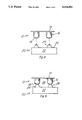
- FIG. 7 illustrates an exemplary array of infrared detectors utilizing the material of the present invention.
- FIGS. 8 and 9 illustrate two cells of the array shown in FIG. 7.
- One object of the invention is to develop improved ceramic grain size, density, and homogeneity with no degradation in infrared detection performance.
- the improved material should improve image quality and processing yield as well as pyroelectric Figure of Merit (FoM).
- standard pyroelectric detectors utilize ferroelectric sensing material that has a high Curie temperature (e.g., lead zirconate titanate or PZT, T c ⁇ 350° C.).
- the sensor layer is poled (i.e. polarized by application of high dc electric field at elevated temperature and slowly cooled with the field applied).
- T c Curie temperature
- the pyroelectric currents are relatively small, necessitating large pixel area (low resolution for a compact structure).
- a second operating mode is called a dielectric bolometer mode and until now has not been significantly applied in commercial products.
- the detector material operates at the Curie point to take advantage of the high pyroelectric signal, enabling small pixel size and high resolution in a compact structure.
- DC bias is required to maintain the polarization.
- this invention applies to materials primarily useful in this second mode.
- BST undoped ceramic barium strontium titanate
- Ca-BST calcium-substituted BST
- E the electric field
- T temperature
- p max the maximum pyroelectric coefficient
- ⁇ the dielectric constant
- ⁇ 0 the permitivity of free space (8.85 ⁇ 10 -12 F/m).
- FoM The highest value of FoM known to be reported in the literature for BST is 90 nC/(cm 2 .K) and the highest value for any material is about 130, for lead scandium tantalate (Whatmore, et al., Ferroelectrics, 1990, vol 104, pp 269-283).
- Figure of Merit values greater than 90 nC/(cm 2 .K) and greater than 130 nC/(cm 2 .K) are possible.
- values in the range 150-300 nC/(cm 2 .K) for BST and Ca-BST are routinely achieved and occasionally values as high as 800-1000 or even 1800 nC/(cm 2 .K) have been achieved.
- BST One problem exhibited by BST is degradation of the pyroelectric response due to thinning.
- the pixel thickness was limited to values greater than 75 ⁇ m because of this degradation.
- the degradation is apparently caused by mechanical deformation of the surface layer during thinning.
- One approach is to remove the surface layer by etching and achieve acceptable response for pixel thicknesses in the range 37-50 ⁇ m. This is tricky in practice, however, since etching can leave ionically conductive residues behind that lead to unacceptable leakage currents. Introduction of the etching step also complicates the processing.
- grain size which is typically in the range 10-30 ⁇ m for undoped materials with acceptable pyroelectric response.
- grain pullouts occur leaving voids behind. These voids can lead to missing pixels.
- etching if etching is required, they provide an easy path for acid to penetrate through the entire thickness of the wafer thereby causing problems with leakage currents due to the ionic residue.
- Large grain size also infers that each pixel contains only a few grains; pixel to pixel variation in electrical response will be high due to the random nature of the grain orientations, and therefore the spontaneous and induced polarizations.
- the potential benefits compared to conventional large-grained materials include: 1) Grain density per pixel increases by approximately three orders of magnitude, averaging the grain orientations, and reducing pixel to pixel property variation accordingly. 2) Polishing damage is limited to only the surface grains, leaving the interior grains unaffected. This could make thinning of less than 75 ⁇ m feasible without etching. 3) Pullouts would be restricted to only the surface layers, so even with etching penetration of acid through the whole thickness would be greatly restricted. 4) Grain surfaces area increases by two orders of magnitude providing greatly increased capability to distribute second phases that occur due to deviation from ideal stoichiometry.
- fine-grain material should exhibit significantly increased tolerance to compositional and processing variations, making it easier to manufacture controllably.
- Fine-grain ceramics tend to sinter to higher densities than coarse-grained (99% of theoretical is common) and also exhibit significantly better resistance to electrical aging.
- Fine-grained ceramics are stronger than coarse grained, providing improved ability to handle thin sections in a high volume manufacturing operation.
- Donor doping of pyroelectric materials such as BST inhibits oxygen vacancy formation and therefore restricts grain growth.
- a trivalent element may be substituted for Ba or a pentavalent element substituted for Ti.
- the lanthanides of atomic number greater than Er may be used but are typically not effective grain refiners.
- the present invention is not limited to only the aforementioned materials and as such other materials may also be used. Sufficiently high doping concentrations, typically greater 0.5 mole %, produce excellent grain refinement, and grain sizes below 1 ⁇ m can be readily attained.
- FIG. 1 illustrates the microstructure of a regular, undoped sample of BST at a magnification of 2000 ⁇ . It should be noted that grain sizes of greater than 10 ⁇ m are common.
- FIG. 2 illustrates the microstructure of a BST sample doped with 0.5% Dy and 0.1% Mn. Once again, the magnification is 2000 ⁇ . Clearly the grain size is much smaller in the doped sample.
- FIG. 3a illustrates the sample at a magnification of 9000 ⁇
- FIG. 3b illustrates the sample at a magnification of 2000 ⁇ .
- the BST was doped with 0.5% Ho and 0.1% Mn.
- acceptor co-doping may not be necessary is when the donor density is relatively high (e.g., [D]>0.01).
- a material with no acceptor co-doping could be useful, for example to produce grain refinement less than one micron for very thin layers.
- the pyroelectric response may not be as good as it would be for acceptor doped materials and therefore these factors must be considered.
- the preferred values are process dependent and will differ depending upon the native impurities present and their concentrations.
- D comprises a trivalent donor ion (e.g., Bi, Sb, Y, La, Ce, Pr, Nd, Sm, Gd, Tb, Dy, Ho, and Er or a combination thereof) and A comprises a trivalent acceptor ion (e.g., Co, Cu, Fe, Mn, Ru, Al, Ga, Sc, U, In, Ni, and Yb or a combination thereof) or a divalent acceptor ion (e.g., Mg). It is noted that both trivalent and divalent ions reside on the Ti sub-lattice. The values for the compositional ratios are given in Table 1.
- D comprises a pentavalent donor ion (e.g., Nb, Ta or a combination thereof) and A comprises a trivalent or divalent acceptor ion (e.g., Co, Cu, Fe, Mn, Ru, Al, Ga, Mg, Sc, U, In, Ni, and Yb or a combination thereof).
- A comprises a trivalent or divalent acceptor ion (e.g., Co, Cu, Fe, Mn, Ru, Al, Ga, Mg, Sc, U, In, Ni, and Yb or a combination thereof).
- D comprises a trivalent donor ion (e.g., Bi, Sb, Y, La, Ce, Pr, Nd, Sm, Gd, Tb, Dy, Ho, and Er or a combination thereof) and A comprises a univalent acceptor ion (e.g., K, Na or a combination thereof).
- a trivalent donor ion e.g., Bi, Sb, Y, La, Ce, Pr, Nd, Sm, Gd, Tb, Dy, Ho, and Er or a combination thereof
- A comprises a univalent acceptor ion (e.g., K, Na or a combination thereof).
- D comprises a pentavalent donor ion (e.g., Nb, Ta, or a combination thereof) and A comprises a univalent acceptor ion (e.g., K, Na or a combination thereof).
- a pentavalent donor ion e.g., Nb, Ta, or a combination thereof
- A comprises a univalent acceptor ion (e.g., K, Na or a combination thereof).
- Test capacitors were made by slicing the respective blocks and polishing the slices with decreasing particle size alumina powders, the final polish using 1 ⁇ m particles. The thinned and polished slices were contacted using screen-printed Ag/Pd thick film ink, fired at 750° C. Each test capacitor spot was nominally 0.14 inch in diameter by 0.010 inch thick. Capacitance and loss tangent were measured during heating at a rate of 0.38° C./min with a Hewlett Packard model 4284A bridge using an oscillator level of 50 mV and DC biases of zero, 2.5 V/mil (1000 V/cm) and 5 V/mil (2000 V/cm).
- the pyroelectric coefficient was determined during heating at 1° C./min using a Hewlett-Packard model 4140B picoammeter and DC biases of 2.5 V/mil (1000 V/mil) and 5 V/mil (2000 V/cm).
- FIGS. 4 through 6 Examples of pyroelectric and dielectric measurements are shown in FIGS. 4 through 6 for a material doped with 0.7 mole % Y and 0.1 mole % Mn.
- FIG. 4 illustrates pyroelectric coefficient as a function of temperature
- FIG. 5 illustrates dielectric constant as a function of temperature
- FIG. 6 illustrates loss tangent as a function of temperature.
- a summary of the results for the other doped materials is given in Table 2.
- materials may also be prepared with lower donor concentration of 0.4 mole %. However, in experimentation these materials possessed high dielectric loss tangents and resistivities below 10 +11 ohm-cm, and therefore may be too conductive for practical application.
- Example 18T1 In another experiment (sample 18T1), a FoM of 1800 was achieved at 2.5 V/mil (1 kV/cm). This material was doped with 0.5% Er and 0.1% Mn.
- FIG. 7 An exemplary array of infrared detectors 10 is illustrated in FIG. 7. Two individual pixels are illustrated in FIG. 8.
- detector array 10 typically comprises two fabricated components which are bonded together.
- the first component 12 includes an infrared absorber and top contact layer 14.
- Individual BST ceramic pixels 16 are formed abutting the layer 14.
- the pixels 16 are formed in rows and columns as illustrated in FIG. 7, although this is not a requirement.
- the pixels 16 may be formed from a BST material as described hereinabove.
- a conductive contact 18 is formed corresponding to each of the pixels 16.
- the second portion 20 of the detector array includes the semiconductor (e.g., silicon) integrated circuitry denoted generally by reference numeral 22.
- the detector circuitry (not shown) included in the semiconductor layer 20 may be as simple as only one address switch per matrix cell or can be expanded to also include features such as high gain preamplifiers, low pass noise filters, buffers, address switches, and other components. In general, a portion of the detection circuitry will correspond to each pixel 16.
- thermal isolation mesa 24 which is formed on the surface of semiconductor layer 20.
- the thermal isolation mesa 24 are typically formed from polyimide and serve to thermally isolate individual pixels from their adjacent neighbors as well as the semiconductor layer 20.
- Conductive contacts 26 are also formed on the surface of semiconductor layer 20 and thermal isolation mesas 24. The contacts 26 will electrically connect each pixel 16 to its corresponding portion of the detection circuitry in integrated circuitry 20 via conductive contacts 28.
- FIG. 8 a cross-sectional view of two pixels is illustrated.
- the first portion 12 and second portion 20 of the detector array will be attached as illustrated by the arrows.
- the preferred embodiment process for attaching the portions is bump bonding which is well known in the art.
- regions of metal such as indium are formed on the contacts 18 and 26 and the two portions are physically pressed together (and possibly heated) to form a stable mechanical bond.
- the bonded detector is illustrated in FIG. 9.
- air gaps 28 separate the individual pixels 16 from one another to provide increased thermal isolation.
Abstract
Description
(Ba.sub.a Sr.sub.b Ca.sub.c).sub.1-x D.sub.x Ti.sub.1-y A.sub.y O.sub.3
              TABLE 1
______________________________________
Variable Minimum      Maximum   Preferred
______________________________________
a        0.55         0.75      0.6
b        0.25         0.40      0.3
c        0.00         0.20      0.1
x        0.003        0.030     .005 to .010
y        0.000        0.010     .001 to .002
______________________________________
(Ba.sub.a Sr.sub.b Ca.sub.c)Ti.sub.1-x-y D.sub.x A.sub.y O.sub.3
(Ba.sub.a Sr.sub.b Ca.sub.c)Ti.sub.1-x D.sub.x O.sub.3.
(Ba.sub.a Sr.sub.b Ca.sub.c).sub.1-x-y D.sub.x A.sub.y TiO.sub.3
(Ba.sub.a Sr.sub.b Ca.sub.c).sub.1-y A.sub.y Ti.sub.1-x D.sub.x O.sub.3
[(Ba.sub.a Sr.sub.b Ca.sub.c).sub.1-x D.sub.x V.sub.(x-y)/2 ][Ti.sub.1-y A.sub.y ]O.sub.3
(Ba.sub.0.6 Sr.sub.0.3 Ca.sub.0.1).sub.1-x D.sub.x Ti.sub.0.999 Mn.sub.0.001 O.sub.3
                                  TABLE 2
__________________________________________________________________________
         mole    mole
                    Sample      ρ
Sample
     Donor
         %  Acceptor
                 %  g.s p.sub.max
                           FoM
                              E Ohm-cm
__________________________________________________________________________
11F1 Y   0.6
            Mn   0.1
                    4.2 1.2
                           82 5.0
                                2.5E+13
12D1 Y   0.7
            Mn   0.1
                    1.0 2.0
                           119
                              5.0
                                2.0E+13
12E1 Y   0.7
            Co   0.1
                    1.0 -- -- --
                                1.4E+4*
12F1 Y   0.8
            Mn   0.1
                    1.1 1.5
                           98 5.0
                                3.0E+13
12G1 La  0.6
            Mn   0.1
                    0.8 0.85
                           51 5.0
                                4.2E+13
12H1 La  0.7
            Mn   0.1
                    0.9 0.55
                           33 5.0
                                2.4E+13
13H1 Y   0.7
            Mn   0.1
                    1.7 1.8
                           98 5.0
                                2.8E+13
13I1**
     Y   0.7
            Mn   0.1
                    1.7 1.9
                           118
                              5.0
                                4.2E+13
13J1***
     Y   0.7
            Mn   0.1
                    1.7 2.7
                           145
                              5.0
                                9.6E+13
13K1 La  0.5
            Mn   0.1
                    1.8 1.3
                           100
                              5.0
                                2.3E+13
14G1 Sm  0.5
            Mn   0.1
                    1.8 3.8
                           173
                              2.5
                                1.4E+13
14G1 Sm  0.5
            Mn   0.1
                    1.8 2.1
                           138
                              5.0
                                1.4E+13
14H1 Gd  0.5
            Mn   0.1
                    2.5 1.3
                           96 5.0
                                4.3E+13
14I1 Dy  0.5
            Mn   0.1
                    2.5 6.3
                           221
                              2.5
                                1.9E+13
14I1 Dy  0.5
            Mn   0.1
                    2.5 3.9
                           225
                              5.0
                                1.9E+13
14J1 Tb  0.5
            Mn   0.1
                    2.2 6.8
                           296
                              2.5
                                1.8E+13
14J1 Tb  0.5
            Mn   0.1
                    2.2 3.4
                           196
                              5.0
                                1.8E+13
14K1 La  0.5
            Mn   0.1
                    2.4 1.6
                           115
                              5.0
                                2.0E+13
__________________________________________________________________________
 Sample ≡ Lot Number
 Sample g.s. ≡ Average Grain Size (μm)
 p.sub.max ≡ Peak Pyroelectric Coefficient
 FoM ≡ Figure of Merit
 E ≡ Electric Field (V/mil)
 ρ ≡ resistivity
 *Conductive
 **+0.1% excess Ti
 ***+0.2% excess Ti
Claims (14)
(Ba.sub.a Sr.sub.b Ca.sub.c).sub.1-x D.sub.x Ti.sub.1-y A.sub.y O.sub.3
[(Ba.sub.a Sr.sub.b Ca.sub.c).sub.1-x D.sub.x V.sub.(x-y)/2 ][Ti.sub.1-y A.sub.y ]O.sub.3
(Ba.sub.a Sr.sub.b Ca.sub.c)Ti.sub.1-x-y D.sub.x A.sub.y O.sub.3
(Ba.sub.a Sr.sub.b Ca.sub.c).sub.1-x-y D.sub.x A.sub.y TiO.sub.3
(Ba.sub.a Sr.sub.b Ca.sub.c).sub.1-y D.sub.x A.sub.y Ti.sub.1-x O.sub.3
Priority Applications (2)
| Application Number | Priority Date | Filing Date | Title |
|---|---|---|---|
| US07/890,891 US5314651A (en) | 1992-05-29 | 1992-05-29 | Fine-grain pyroelectric detector material and method |
| US08/198,927 US5434410A (en) | 1992-05-29 | 1994-02-18 | Fine-grain pyroelectric detector material and method |
Applications Claiming Priority (1)
| Application Number | Priority Date | Filing Date | Title |
|---|---|---|---|
| US07/890,891 US5314651A (en) | 1992-05-29 | 1992-05-29 | Fine-grain pyroelectric detector material and method |
Related Child Applications (1)
| Application Number | Title | Priority Date | Filing Date |
|---|---|---|---|
| US08/198,927 Division US5434410A (en) | 1992-05-29 | 1994-02-18 | Fine-grain pyroelectric detector material and method |
Publications (1)
| Publication Number | Publication Date |
|---|---|
| US5314651A true US5314651A (en) | 1994-05-24 |
Family
ID=25397290
Family Applications (2)
| Application Number | Title | Priority Date | Filing Date |
|---|---|---|---|
| US07/890,891 Expired - Lifetime US5314651A (en) | 1992-05-29 | 1992-05-29 | Fine-grain pyroelectric detector material and method |
| US08/198,927 Expired - Lifetime US5434410A (en) | 1992-05-29 | 1994-02-18 | Fine-grain pyroelectric detector material and method |
Family Applications After (1)
| Application Number | Title | Priority Date | Filing Date |
|---|---|---|---|
| US08/198,927 Expired - Lifetime US5434410A (en) | 1992-05-29 | 1994-02-18 | Fine-grain pyroelectric detector material and method |
Country Status (1)
| Country | Link |
|---|---|
| US (2) | US5314651A (en) |
Cited By (21)
| Publication number | Priority date | Publication date | Assignee | Title |
|---|---|---|---|---|
| EP0709355A1 (en) * | 1994-09-30 | 1996-05-01 | Texas Instruments Incorporated | Barium and/or strontium titanate dielectric thin film comprising erbium, and formation process |
| US5556818A (en) * | 1993-10-09 | 1996-09-17 | U.S. Philips Corporation | Substituted barium-neodymium-titanium-perovskite, dielectric, ceramic composition, capacitor and microwave components |
| DE19608182A1 (en) * | 1995-03-04 | 1996-09-19 | Lg Semicon Co Ltd | Dielectric thin film for use in semiconductor memory device capacitor |
| US5610111A (en) * | 1993-11-25 | 1997-03-11 | Ngk Spark Plug Co., Ltd. | Ceramic composition for thermistor |
| US5625529A (en) * | 1995-03-28 | 1997-04-29 | Samsung Electronics Co., Ltd. | PZT thin films for ferroelectric capacitor and method for preparing the same |
| US5807642A (en) * | 1995-11-20 | 1998-09-15 | Xue; Liang An | Solid oxide fuel cell stacks with barium and strontium ceramic bodies |
| US5888659A (en) * | 1993-09-28 | 1999-03-30 | Texas Instruments Incorporated | Donor doped perovskites for thin-film ferroelectric and pyroelectric devices |
| US6139780A (en) * | 1998-05-28 | 2000-10-31 | Sharp Kabushiki Kaisha | Dynamic random access memories with dielectric compositions stable to reduction |
| US6331234B1 (en) | 1999-06-02 | 2001-12-18 | Honeywell International Inc. | Copper sputtering target assembly and method of making same |
| US6346496B2 (en) * | 1998-07-24 | 2002-02-12 | Murata Manufacturing Co., Ltd. | Composite material for positive temperature coefficient thermistor, ceramic for positive temperature coefficient thermistor and method for manufacturing ceramics for positive temperature coefficient thermistor |
| US6362521B1 (en) * | 1998-11-11 | 2002-03-26 | Murata Manufacturing Co., Ltd. | Semiconductor ceramic and device using the same |
| US20020112791A1 (en) * | 1999-06-02 | 2002-08-22 | Kardokus Janine K. | Methods of forming copper-containing sputtering targets |
| US6451222B1 (en) * | 1999-12-16 | 2002-09-17 | Honeywell International Inc. | Ferroelectric composition, ferroelectric vapor deposition target and method of making a ferroelectric vapor deposition target |
| US6472339B2 (en) * | 1997-10-09 | 2002-10-29 | Murata Manufacturing Co., Ltd. | Barium titanate semiconductive ceramic |
| US6613707B2 (en) * | 2001-02-27 | 2003-09-02 | Amotech Co., Ltd. | Dielectric ceramic compositions |
| US6641940B1 (en) * | 2001-10-09 | 2003-11-04 | Intematix Corporation | Low loss dielectric materials for microwave applications |
| US6676935B2 (en) | 1995-06-27 | 2004-01-13 | Cell Genesys, Inc. | Tissue specific adenoviral vectors |
| US6758920B2 (en) | 1999-11-24 | 2004-07-06 | Honeywell International Inc. | Conductive integrated circuit metal alloy interconnections, electroplating anodes; metal alloys for use as a conductive interconnection in an integrated circuit; and physical vapor deposition targets |
| US20050047569A1 (en) * | 2003-09-03 | 2005-03-03 | Tekelec | Methods and systems for identifying calls connected without answer supervision and for automatically generating billing information for the calls |
| WO2005048357A1 (en) * | 2003-11-10 | 2005-05-26 | Ii-Vi Incorporated | Radiation detector |
| US20070039817A1 (en) * | 2003-08-21 | 2007-02-22 | Daniels Brian J | Copper-containing pvd targets and methods for their manufacture |
Families Citing this family (37)
| Publication number | Priority date | Publication date | Assignee | Title |
|---|---|---|---|---|
| US5624707A (en) * | 1991-12-13 | 1997-04-29 | Symetrix Corporation | Method of forming ABO3 films with excess B-site modifiers |
| US5644838A (en) * | 1995-01-03 | 1997-07-08 | Texas Instruments Incorporated | Method of fabricating a focal plane array for hybrid thermal imaging system |
| US10388626B2 (en) * | 2000-03-10 | 2019-08-20 | STATS ChipPAC Pte. Ltd. | Semiconductor device and method of forming flipchip interconnect structure |
| WO2001068311A1 (en) | 2000-03-10 | 2001-09-20 | Chippac, Inc. | Flip chip interconnection structure |
| TWI358776B (en) * | 2003-11-08 | 2012-02-21 | Chippac Inc | Flip chip interconnection pad layout |
| US8853001B2 (en) * | 2003-11-08 | 2014-10-07 | Stats Chippac, Ltd. | Semiconductor device and method of forming pad layout for flipchip semiconductor die |
| US8350384B2 (en) * | 2009-11-24 | 2013-01-08 | Stats Chippac, Ltd. | Semiconductor device and method of forming electrical interconnect with stress relief void |
| US7659633B2 (en) | 2004-11-10 | 2010-02-09 | Stats Chippac, Ltd. | Solder joint flip chip interconnection having relief structure |
| US9029196B2 (en) | 2003-11-10 | 2015-05-12 | Stats Chippac, Ltd. | Semiconductor device and method of self-confinement of conductive bump material during reflow without solder mask |
| US8076232B2 (en) * | 2008-04-03 | 2011-12-13 | Stats Chippac, Ltd. | Semiconductor device and method of forming composite bump-on-lead interconnection |
| USRE47600E1 (en) | 2003-11-10 | 2019-09-10 | STATS ChipPAC Pte. Ltd. | Semiconductor device and method of forming electrical interconnect with stress relief void |
| US8026128B2 (en) | 2004-11-10 | 2011-09-27 | Stats Chippac, Ltd. | Semiconductor device and method of self-confinement of conductive bump material during reflow without solder mask |
| KR101249555B1 (en) | 2003-11-10 | 2013-04-01 | 스태츠 칩팩, 엘티디. | Bump-on-lead flip chip interconnection |
| USRE44500E1 (en) | 2003-11-10 | 2013-09-17 | Stats Chippac, Ltd. | Semiconductor device and method of forming composite bump-on-lead interconnection |
| US20060216860A1 (en) * | 2005-03-25 | 2006-09-28 | Stats Chippac, Ltd. | Flip chip interconnection having narrow interconnection sites on the substrate |
| US8216930B2 (en) | 2006-12-14 | 2012-07-10 | Stats Chippac, Ltd. | Solder joint flip chip interconnection having relief structure |
| US8574959B2 (en) | 2003-11-10 | 2013-11-05 | Stats Chippac, Ltd. | Semiconductor device and method of forming bump-on-lead interconnection |
| US8129841B2 (en) | 2006-12-14 | 2012-03-06 | Stats Chippac, Ltd. | Solder joint flip chip interconnection |
| US20070105277A1 (en) | 2004-11-10 | 2007-05-10 | Stats Chippac Ltd. | Solder joint flip chip interconnection |
| US8841779B2 (en) | 2005-03-25 | 2014-09-23 | Stats Chippac, Ltd. | Semiconductor device and method of forming high routing density BOL BONL and BONP interconnect sites on substrate |
| US9258904B2 (en) * | 2005-05-16 | 2016-02-09 | Stats Chippac, Ltd. | Semiconductor device and method of forming narrow interconnect sites on substrate with elongated mask openings |
| US20060255473A1 (en) | 2005-05-16 | 2006-11-16 | Stats Chippac Ltd. | Flip chip interconnect solder mask |
| US7713782B2 (en) * | 2006-09-22 | 2010-05-11 | Stats Chippac, Inc. | Fusible I/O interconnection systems and methods for flip-chip packaging involving substrate-mounted stud-bumps |
| US9847309B2 (en) | 2006-09-22 | 2017-12-19 | STATS ChipPAC Pte. Ltd. | Semiconductor device and method of forming vertical interconnect structure between semiconductor die and substrate |
| US8349721B2 (en) | 2008-03-19 | 2013-01-08 | Stats Chippac, Ltd. | Semiconductor device and method of forming insulating layer on conductive traces for electrical isolation in fine pitch bonding |
| US7759137B2 (en) * | 2008-03-25 | 2010-07-20 | Stats Chippac, Ltd. | Flip chip interconnection structure with bump on partial pad and method thereof |
| US9345148B2 (en) | 2008-03-25 | 2016-05-17 | Stats Chippac, Ltd. | Semiconductor device and method of forming flipchip interconnection structure with bump on partial pad |
| US20090250814A1 (en) * | 2008-04-03 | 2009-10-08 | Stats Chippac, Ltd. | Flip Chip Interconnection Structure Having Void-Free Fine Pitch and Method Thereof |
| US7897502B2 (en) * | 2008-09-10 | 2011-03-01 | Stats Chippac, Ltd. | Method of forming vertically offset bond on trace interconnects on recessed and raised bond fingers |
| US8198186B2 (en) | 2008-12-31 | 2012-06-12 | Stats Chippac, Ltd. | Semiconductor device and method of confining conductive bump material during reflow with solder mask patch |
| US8659172B2 (en) | 2008-12-31 | 2014-02-25 | Stats Chippac, Ltd. | Semiconductor device and method of confining conductive bump material with solder mask patch |
| US20100237500A1 (en) * | 2009-03-20 | 2010-09-23 | Stats Chippac, Ltd. | Semiconductor Substrate and Method of Forming Conformal Solder Wet-Enhancement Layer on Bump-on-Lead Site |
| US8039384B2 (en) | 2010-03-09 | 2011-10-18 | Stats Chippac, Ltd. | Semiconductor device and method of forming vertically offset bond on trace interconnects on different height traces |
| US8409978B2 (en) | 2010-06-24 | 2013-04-02 | Stats Chippac, Ltd. | Semiconductor device and method of forming vertically offset bond on trace interconnect structure on leadframe |
| US8492197B2 (en) | 2010-08-17 | 2013-07-23 | Stats Chippac, Ltd. | Semiconductor device and method of forming vertically offset conductive pillars over first substrate aligned to vertically offset BOT interconnect sites formed over second substrate |
| US8435834B2 (en) | 2010-09-13 | 2013-05-07 | Stats Chippac, Ltd. | Semiconductor device and method of forming bond-on-lead interconnection for mounting semiconductor die in FO-WLCSP |
| US10175277B2 (en) | 2015-08-31 | 2019-01-08 | Pgs Geophysical As | Identification of degrading electrodes in a marine electromagnetic survey system |
Citations (8)
| Publication number | Priority date | Publication date | Assignee | Title |
|---|---|---|---|---|
| JPS584448A (en) * | 1981-06-30 | 1983-01-11 | Fujitsu Ltd | Data processing circuit |
| JPS5992503A (en) * | 1982-11-18 | 1984-05-28 | 太陽誘電株式会社 | Semiconductor porcelain unit with voltage depending nonlinear resistance property |
| JPS6042802A (en) * | 1983-08-18 | 1985-03-07 | 松下電器産業株式会社 | Voltage dependent nonlinear resistor porcelain composition |
| EP0187960A2 (en) * | 1984-12-18 | 1986-07-23 | Taiyo Yuden Co., Ltd. | Low temperature sintered ceramic capacitor with high DC breakdown voltage, and method of manufacture |
| US4677083A (en) * | 1984-01-24 | 1987-06-30 | Sony Corporation | Method for manufacturing dielectric fine powder of Ba1-x Srx TiO3 |
| JPH02188427A (en) * | 1989-01-18 | 1990-07-24 | Sakai Chem Ind Co Ltd | Inorganic composition |
| US4983839A (en) * | 1989-08-18 | 1991-01-08 | The United States Of America As Represented By The Secretary Of The Army | Pyroelectric materials |
| GB2240335A (en) * | 1988-11-30 | 1991-07-31 | Plessey Co Plc | Ferroelectric materials |
Family Cites Families (3)
| Publication number | Priority date | Publication date | Assignee | Title |
|---|---|---|---|---|
| US4740700A (en) * | 1986-09-02 | 1988-04-26 | Hughes Aircraft Company | Thermally insulative and electrically conductive interconnect and process for making same |
| GB8827661D0 (en) * | 1988-11-26 | 1989-05-17 | Emi Plc Thorn | Thermal imaging devices |
| DD298681A5 (en) * | 1989-03-26 | 1992-03-05 | Technische Universitaet Dresden,De | METHOD FOR PRODUCING A PYROELECTRIC MULTI-ELEMENT SENSOR |
-
1992
- 1992-05-29 US US07/890,891 patent/US5314651A/en not_active Expired - Lifetime
-
1994
- 1994-02-18 US US08/198,927 patent/US5434410A/en not_active Expired - Lifetime
Patent Citations (8)
| Publication number | Priority date | Publication date | Assignee | Title |
|---|---|---|---|---|
| JPS584448A (en) * | 1981-06-30 | 1983-01-11 | Fujitsu Ltd | Data processing circuit |
| JPS5992503A (en) * | 1982-11-18 | 1984-05-28 | 太陽誘電株式会社 | Semiconductor porcelain unit with voltage depending nonlinear resistance property |
| JPS6042802A (en) * | 1983-08-18 | 1985-03-07 | 松下電器産業株式会社 | Voltage dependent nonlinear resistor porcelain composition |
| US4677083A (en) * | 1984-01-24 | 1987-06-30 | Sony Corporation | Method for manufacturing dielectric fine powder of Ba1-x Srx TiO3 |
| EP0187960A2 (en) * | 1984-12-18 | 1986-07-23 | Taiyo Yuden Co., Ltd. | Low temperature sintered ceramic capacitor with high DC breakdown voltage, and method of manufacture |
| GB2240335A (en) * | 1988-11-30 | 1991-07-31 | Plessey Co Plc | Ferroelectric materials |
| JPH02188427A (en) * | 1989-01-18 | 1990-07-24 | Sakai Chem Ind Co Ltd | Inorganic composition |
| US4983839A (en) * | 1989-08-18 | 1991-01-08 | The United States Of America As Represented By The Secretary Of The Army | Pyroelectric materials |
Non-Patent Citations (18)
| Title |
|---|
| B. M. Kulwicki, "Instabilities in PTC Resistors", Proceedings of the 6th IEEE International Symposium on Applications of Ferroelectrics, Bethlehem, PA., Jun. 8-11, 1986, pp. 656-664. |
| B. M. Kulwicki, "PTC Materials Technology, 1955-1980", Advances in Ceramics, vol. 1, Grain Boundary Phenomena in Electronic Ceramics, 1981, pp. 138-154. |
| B. M. Kulwicki, "Trends in PTC Resistor Technology", SAMPE Journal, Nov./Dec., 1987, vol. 23-6, pp. 34-38. |
| B. M. Kulwicki, Instabilities in PTC Resistors , Proceedings of the 6th IEEE International Symposium on Applications of Ferroelectrics, Bethlehem, PA., Jun. 8 11, 1986, pp. 656 664. * |
| B. M. Kulwicki, PTC Materials Technology, 1955 1980 , Advances in Ceramics, vol. 1, Grain Boundary Phenomena in Electronic Ceramics, 1981, pp. 138 154. * |
| B. M. Kulwicki, Trends in PTC Resistor Technology , SAMPE Journal, Nov./Dec., 1987, vol. 23 6, pp. 34 38. * |
| E. D. Mocklen, "Materials and Fundamental Properties of Switching PTC Thermistors", Thermistors, Electrochemical Publications Ltd., Ayr, Scotland, 1979, pp. 154-170. |
| E. D. Mocklen, Materials and Fundamental Properties of Switching PTC Thermistors , Thermistors, Electrochemical Publications Ltd., Ayr, Scotland, 1979, pp. 154 170. * |
| L. A. Xue et al., "The Influence of Ionic Radii on the Incorporation of Trivalent Dopants into BaTiO3 ", Material Science Engineering, B1 (1988), pp. 193-201. |
| L. A. Xue et al., The Influence of Ionic Radii on the Incorporation of Trivalent Dopants into BaTiO 3 , Material Science Engineering, B1 (1988), pp. 193 201. * |
| R. W. Whatmore et al., "Ferroelectric Materials for Thermal IR Sensors, State-of-the-Art and Perspectives", Ferroelectrics, 1990, vol. 104 pp. 269-283. |
| R. W. Whatmore et al., Ferroelectric Materials for Thermal IR Sensors, State of the Art and Perspectives , Ferroelectrics, 1990, vol. 104 pp. 269 283. * |
| R. W. Whatmore, "Pyroelectric Ceramics and Devices for Thermal Infrared Detection and Imaging", Ferroelectrics, 1991, vol. 118, pp. 241-259. |
| R. W. Whatmore, Pyroelectric Ceramics and Devices for Thermal Infrared Detection and Imaging , Ferroelectrics, 1991, vol. 118, pp. 241 259. * |
| T. Murakami et al., "Dy-Doped BaTiO3 Ceramics for High Voltage Capacitor Use", Ceramic Bulletin, vol. 55, No. 6 (1976), pp. 572-575. |
| T. Murakami et al., Dy Doped BaTiO 3 Ceramics for High Voltage Capacitor Use , Ceramic Bulletin, vol. 55, No. 6 (1976), pp. 572 575. * |
| Toshio Ashida et al., "The Effects of Additives and of Ambient Atmosphere During Heating on the Electrical Resistivity of Semiconducting BaTiO3 ", Japanese Journal of Applied Physics, vol. 5, No. 1, Apr., 1966, pp. 269-274. |
| Toshio Ashida et al., The Effects of Additives and of Ambient Atmosphere During Heating on the Electrical Resistivity of Semiconducting BaTiO 3 , Japanese Journal of Applied Physics, vol. 5, No. 1, Apr., 1966, pp. 269 274. * |
Cited By (32)
| Publication number | Priority date | Publication date | Assignee | Title |
|---|---|---|---|---|
| US5888659A (en) * | 1993-09-28 | 1999-03-30 | Texas Instruments Incorporated | Donor doped perovskites for thin-film ferroelectric and pyroelectric devices |
| US5556818A (en) * | 1993-10-09 | 1996-09-17 | U.S. Philips Corporation | Substituted barium-neodymium-titanium-perovskite, dielectric, ceramic composition, capacitor and microwave components |
| US5610111A (en) * | 1993-11-25 | 1997-03-11 | Ngk Spark Plug Co., Ltd. | Ceramic composition for thermistor |
| EP0709355A1 (en) * | 1994-09-30 | 1996-05-01 | Texas Instruments Incorporated | Barium and/or strontium titanate dielectric thin film comprising erbium, and formation process |
| US5635741A (en) * | 1994-09-30 | 1997-06-03 | Texas Instruments Incorporated | Barium strontium titanate (BST) thin films by erbium donor doping |
| US5731220A (en) * | 1994-09-30 | 1998-03-24 | Texas Instruments Incorporated | Method of making barium strontium titanate (BST) thin film by erbium donor doping |
| DE19608182A1 (en) * | 1995-03-04 | 1996-09-19 | Lg Semicon Co Ltd | Dielectric thin film for use in semiconductor memory device capacitor |
| US5874379A (en) * | 1995-03-04 | 1999-02-23 | Lg Semicon Co., Ltd. | Dielectric thin film and fabrication method thereof |
| DE19608182C2 (en) * | 1995-03-04 | 2003-03-20 | Lg Semicon Co Ltd | Dielectric thin film and capacitor with this for semiconductor devices and their manufacturing processes |
| US5625529A (en) * | 1995-03-28 | 1997-04-29 | Samsung Electronics Co., Ltd. | PZT thin films for ferroelectric capacitor and method for preparing the same |
| US6676935B2 (en) | 1995-06-27 | 2004-01-13 | Cell Genesys, Inc. | Tissue specific adenoviral vectors |
| US5807642A (en) * | 1995-11-20 | 1998-09-15 | Xue; Liang An | Solid oxide fuel cell stacks with barium and strontium ceramic bodies |
| US6472339B2 (en) * | 1997-10-09 | 2002-10-29 | Murata Manufacturing Co., Ltd. | Barium titanate semiconductive ceramic |
| US6139780A (en) * | 1998-05-28 | 2000-10-31 | Sharp Kabushiki Kaisha | Dynamic random access memories with dielectric compositions stable to reduction |
| US6346496B2 (en) * | 1998-07-24 | 2002-02-12 | Murata Manufacturing Co., Ltd. | Composite material for positive temperature coefficient thermistor, ceramic for positive temperature coefficient thermistor and method for manufacturing ceramics for positive temperature coefficient thermistor |
| US6362521B1 (en) * | 1998-11-11 | 2002-03-26 | Murata Manufacturing Co., Ltd. | Semiconductor ceramic and device using the same |
| US6645427B1 (en) | 1999-06-02 | 2003-11-11 | Honeywell International Inc. | Copper sputtering target assembly and method of making same |
| US20020112791A1 (en) * | 1999-06-02 | 2002-08-22 | Kardokus Janine K. | Methods of forming copper-containing sputtering targets |
| US6849139B2 (en) | 1999-06-02 | 2005-02-01 | Honeywell International Inc. | Methods of forming copper-containing sputtering targets |
| US6331234B1 (en) | 1999-06-02 | 2001-12-18 | Honeywell International Inc. | Copper sputtering target assembly and method of making same |
| US6758920B2 (en) | 1999-11-24 | 2004-07-06 | Honeywell International Inc. | Conductive integrated circuit metal alloy interconnections, electroplating anodes; metal alloys for use as a conductive interconnection in an integrated circuit; and physical vapor deposition targets |
| US20030205690A1 (en) * | 1999-12-16 | 2003-11-06 | Jianxing Li | Ferroelectric vapor deposition targets |
| US6746619B2 (en) * | 1999-12-16 | 2004-06-08 | Honeywell International Inc. | Ferroelectric vapor deposition targets |
| US6579467B2 (en) | 1999-12-16 | 2003-06-17 | Honeywell International Inc. | Ferroelectric composition, ferroelectric vapor deposition target and method of making a ferroelectric vapor deposition target |
| US6451222B1 (en) * | 1999-12-16 | 2002-09-17 | Honeywell International Inc. | Ferroelectric composition, ferroelectric vapor deposition target and method of making a ferroelectric vapor deposition target |
| US6858102B1 (en) | 2000-11-15 | 2005-02-22 | Honeywell International Inc. | Copper-containing sputtering targets, and methods of forming copper-containing sputtering targets |
| US6613707B2 (en) * | 2001-02-27 | 2003-09-02 | Amotech Co., Ltd. | Dielectric ceramic compositions |
| US6641940B1 (en) * | 2001-10-09 | 2003-11-04 | Intematix Corporation | Low loss dielectric materials for microwave applications |
| US20070039817A1 (en) * | 2003-08-21 | 2007-02-22 | Daniels Brian J | Copper-containing pvd targets and methods for their manufacture |
| US20050047569A1 (en) * | 2003-09-03 | 2005-03-03 | Tekelec | Methods and systems for identifying calls connected without answer supervision and for automatically generating billing information for the calls |
| WO2005048357A1 (en) * | 2003-11-10 | 2005-05-26 | Ii-Vi Incorporated | Radiation detector |
| US20070193507A1 (en) * | 2003-11-10 | 2007-08-23 | Ii-Vi Incorporated | Radiation detector |
Also Published As
| Publication number | Publication date |
|---|---|
| US5434410A (en) | 1995-07-18 |
Similar Documents
| Publication | Publication Date | Title |
|---|---|---|
| US5314651A (en) | Fine-grain pyroelectric detector material and method | |
| Ertuğ | The overview of the electrical properties of barium titanate | |
| US7872854B2 (en) | Semiconductor ceramic, monolithic semiconductor ceramic capacitor, method for manufacturing semiconductor ceramic, and method for manufacturing monolithic semiconductor ceramic capacitor | |
| US7547401B2 (en) | Compositions for high power piezoelectric ceramics | |
| EP0988637B1 (en) | Ceramic multilayer capacitor | |
| CN101687663B (en) | Semiconductor ceramic powder, semiconductor ceramic, and laminated semiconductor capacitor | |
| US10217566B2 (en) | Ceramic material and capacitor comprising the ceramic material | |
| US6685850B2 (en) | Piezoelectric ceramic material | |
| US20110204277A1 (en) | Compositions for high power piezoelectric ceramics | |
| US11562857B2 (en) | Relaxor-ferroelectric material and method of synthesizing the same and device including relaxor-ferroelectric material | |
| US20060229187A1 (en) | Compositions for high power piezoelectric ceramics | |
| US5566046A (en) | Microelectronic device with capacitors having fine-grain dielectric material | |
| US20150311425A1 (en) | Method for manufacturing piezoelectric ceramic, piezoelectric ceramic, and piezoelectric element | |
| CN113963951A (en) | Dielectric material, method of manufacturing the same, device including the same, and memory cell | |
| Hayashi et al. | Low-temperature sintering and properties of (Pb, Ba, Sr)(Zr, Ti, Sb) O3 piezoelectric ceramics using sintering aids | |
| Sakamoto et al. | Fabrication and properties of nonreducible lead-free piezoelectric Mn-doped (Ba, Ca) TiO3 ceramics | |
| Ho et al. | Influence of potassium on preparation and performance of PTC resistors | |
| US8524109B2 (en) | High curie temperature ternary piezoelectric ceramics | |
| JP2000319065A (en) | Ferroelectric ceramic, pyroelectric and pyroelectric infrared ray detector | |
| Liu et al. | Self-biased dielectric bolometer from epitaxially grown Pb (Zr, Ti) O 3 and lanthanum-doped Pb (Zr, Ti) O 3 multilayered thin films | |
| CN106495688B (en) | One kind having both field and causes enhancing pyroelectric property and wide warm area electric card effect new ceramic material and preparation method thereof | |
| Min et al. | Electrical characteristics and microstructures of Sm2O3-doped Bi4Ti3O12 ceramics | |
| Adamczyk et al. | Relaxor behavior of La-modified (Pb 0.75 Ba 0.25)(Zr 0.70 Ti 0.30) O 3 ceramics | |
| US20220415577A1 (en) | Dielectric material and device including the same | |
| Sharma et al. | Dielectric and pyroelectric characteristics of PZT doped with gadolinium |
Legal Events
| Date | Code | Title | Description |
|---|---|---|---|
| AS | Assignment |
Owner name: TEXAS INSTRUMENTS INCORPORATED A CORP. OF DELAWA Free format text: ASSIGNMENT OF ASSIGNORS INTEREST.;ASSIGNOR:KULWICKI, BERNARD M.;REEL/FRAME:006227/0191 Effective date: 19920520 |
|
| STCF | Information on status: patent grant |
Free format text: PATENTED CASE |
|
| FPAY | Fee payment |
Year of fee payment: 4 |
|
| AS | Assignment |
Owner name: RAYTHEON COMPANY, MASSACHUSETTS Free format text: ASSIGNMENT OF ASSIGNORS INTEREST;ASSIGNOR:TEXAS INSTRUMENTS INCORPORATED;REEL/FRAME:009764/0360 Effective date: 19990212 |
|
| FEPP | Fee payment procedure |
Free format text: PAYOR NUMBER ASSIGNED (ORIGINAL EVENT CODE: ASPN); ENTITY STATUS OF PATENT OWNER: LARGE ENTITY |
|
| FPAY | Fee payment |
Year of fee payment: 8 |
|
| FEPP | Fee payment procedure |
Free format text: PAYOR NUMBER ASSIGNED (ORIGINAL EVENT CODE: ASPN); ENTITY STATUS OF PATENT OWNER: LARGE ENTITY Free format text: PAYER NUMBER DE-ASSIGNED (ORIGINAL EVENT CODE: RMPN); ENTITY STATUS OF PATENT OWNER: LARGE ENTITY |
|
| AS | Assignment |
Owner name: L-3 COMMUNICATIONS CORPORATION, NEW YORK Free format text: ASSIGNMENT OF ASSIGNORS INTEREST;ASSIGNORS:RAYTHEON COMPANY;L-3 COMMUNICATIONS CORPORATION;REEL/FRAME:015478/0930 Effective date: 20041109 |
|
| AS | Assignment |
Owner name: L-3 COMMUNICATIONS CORPORATION, NEW YORK Free format text: CORRECTED ASSIGNMENT TO CORRECT ERRONEOUS LISTING OF AN ADDITIONAL ASSIGNOR ON THE RECORDATION COVER SHEET RECORDED AT REEL/FRAME 015478/0930.;ASSIGNOR:RAYTHEON COMPANY;REEL/FRAME:015653/0757 Effective date: 20041109 |
|
| FPAY | Fee payment |
Year of fee payment: 12 |