US5307458A - Input/output coprocessor for printing machine - Google Patents
Input/output coprocessor for printing machine Download PDFInfo
- Publication number
- US5307458A US5307458A US07/812,314 US81231491A US5307458A US 5307458 A US5307458 A US 5307458A US 81231491 A US81231491 A US 81231491A US 5307458 A US5307458 A US 5307458A
- Authority
- US
- United States
- Prior art keywords
- bus
- data
- image data
- memory
- cpu
- Prior art date
- Legal status (The legal status is an assumption and is not a legal conclusion. Google has not performed a legal analysis and makes no representation as to the accuracy of the status listed.)
- Expired - Lifetime
Links
- 238000007639 printing Methods 0.000 title abstract description 38
- 230000015654 memory Effects 0.000 claims abstract description 95
- 238000012546 transfer Methods 0.000 claims abstract description 64
- 238000012545 processing Methods 0.000 claims abstract description 25
- 238000000034 method Methods 0.000 claims description 17
- 238000003860 storage Methods 0.000 claims description 9
- 230000005540 biological transmission Effects 0.000 claims description 6
- 230000003139 buffering effect Effects 0.000 claims description 5
- 230000004044 response Effects 0.000 abstract description 6
- 239000000872 buffer Substances 0.000 description 83
- 238000010586 diagram Methods 0.000 description 15
- 238000004891 communication Methods 0.000 description 10
- 230000008569 process Effects 0.000 description 10
- 238000004140 cleaning Methods 0.000 description 8
- 239000000463 material Substances 0.000 description 8
- 230000006870 function Effects 0.000 description 7
- 230000033001 locomotion Effects 0.000 description 7
- 230000008901 benefit Effects 0.000 description 6
- 238000013461 design Methods 0.000 description 6
- 230000001360 synchronised effect Effects 0.000 description 6
- 238000007906 compression Methods 0.000 description 5
- 230000006835 compression Effects 0.000 description 5
- 230000002093 peripheral effect Effects 0.000 description 5
- 230000003044 adaptive effect Effects 0.000 description 4
- 238000013459 approach Methods 0.000 description 4
- 238000003491 array Methods 0.000 description 4
- 230000009977 dual effect Effects 0.000 description 4
- 238000012163 sequencing technique Methods 0.000 description 4
- 238000011161 development Methods 0.000 description 3
- 238000003384 imaging method Methods 0.000 description 3
- 238000012432 intermediate storage Methods 0.000 description 3
- 239000002245 particle Substances 0.000 description 3
- 108091008695 photoreceptors Proteins 0.000 description 3
- 239000000843 powder Substances 0.000 description 3
- 238000009825 accumulation Methods 0.000 description 2
- 230000002457 bidirectional effect Effects 0.000 description 2
- 238000006243 chemical reaction Methods 0.000 description 2
- 230000008878 coupling Effects 0.000 description 2
- 238000010168 coupling process Methods 0.000 description 2
- 238000005859 coupling reaction Methods 0.000 description 2
- 238000013500 data storage Methods 0.000 description 2
- 230000000694 effects Effects 0.000 description 2
- 238000007726 management method Methods 0.000 description 2
- 230000036961 partial effect Effects 0.000 description 2
- 230000000737 periodic effect Effects 0.000 description 2
- 230000000630 rising effect Effects 0.000 description 2
- 101150108015 STR6 gene Proteins 0.000 description 1
- 101100386054 Saccharomyces cerevisiae (strain ATCC 204508 / S288c) CYS3 gene Proteins 0.000 description 1
- 210000004556 brain Anatomy 0.000 description 1
- 239000003086 colorant Substances 0.000 description 1
- 238000010276 construction Methods 0.000 description 1
- 238000013144 data compression Methods 0.000 description 1
- 230000006837 decompression Effects 0.000 description 1
- 230000003111 delayed effect Effects 0.000 description 1
- 230000002708 enhancing effect Effects 0.000 description 1
- 239000000835 fiber Substances 0.000 description 1
- 239000008187 granular material Substances 0.000 description 1
- 230000002401 inhibitory effect Effects 0.000 description 1
- 238000002955 isolation Methods 0.000 description 1
- 230000000670 limiting effect Effects 0.000 description 1
- 230000007774 longterm Effects 0.000 description 1
- 238000004519 manufacturing process Methods 0.000 description 1
- 239000000203 mixture Substances 0.000 description 1
- 230000003287 optical effect Effects 0.000 description 1
- 229920000740 poly(D-lysine) polymer Polymers 0.000 description 1
- 238000009877 rendering Methods 0.000 description 1
- 238000011160 research Methods 0.000 description 1
- 230000000284 resting effect Effects 0.000 description 1
- 230000003068 static effect Effects 0.000 description 1
- 101150035983 str1 gene Proteins 0.000 description 1
- 238000011144 upstream manufacturing Methods 0.000 description 1
- 239000002699 waste material Substances 0.000 description 1
- 230000003936 working memory Effects 0.000 description 1
Images


Classifications
-
- G—PHYSICS
- G06—COMPUTING; CALCULATING OR COUNTING
- G06F—ELECTRIC DIGITAL DATA PROCESSING
- G06F13/00—Interconnection of, or transfer of information or other signals between, memories, input/output devices or central processing units
- G06F13/10—Program control for peripheral devices
- G06F13/12—Program control for peripheral devices using hardware independent of the central processor, e.g. channel or peripheral processor
- G06F13/124—Program control for peripheral devices using hardware independent of the central processor, e.g. channel or peripheral processor where hardware is a sequential transfer control unit, e.g. microprocessor, peripheral processor or state-machine
-
- H—ELECTRICITY
- H04—ELECTRIC COMMUNICATION TECHNIQUE
- H04N—PICTORIAL COMMUNICATION, e.g. TELEVISION
- H04N1/00—Scanning, transmission or reproduction of documents or the like, e.g. facsimile transmission; Details thereof
- H04N1/32—Circuits or arrangements for control or supervision between transmitter and receiver or between image input and image output device, e.g. between a still-image camera and its memory or between a still-image camera and a printer device
- H04N1/32358—Circuits or arrangements for control or supervision between transmitter and receiver or between image input and image output device, e.g. between a still-image camera and its memory or between a still-image camera and a printer device using picture signal storage, e.g. at transmitter
-
- H—ELECTRICITY
- H04—ELECTRIC COMMUNICATION TECHNIQUE
- H04N—PICTORIAL COMMUNICATION, e.g. TELEVISION
- H04N2201/00—Indexing scheme relating to scanning, transmission or reproduction of documents or the like, and to details thereof
- H04N2201/32—Circuits or arrangements for control or supervision between transmitter and receiver or between image input and image output device, e.g. between a still-image camera and its memory or between a still-image camera and a printer device
- H04N2201/3285—Circuits or arrangements for control or supervision between transmitter and receiver or between image input and image output device, e.g. between a still-image camera and its memory or between a still-image camera and a printer device using picture signal storage, e.g. at transmitter
- H04N2201/3287—Storage of at least one complete document page or image frame
-
- H—ELECTRICITY
- H04—ELECTRIC COMMUNICATION TECHNIQUE
- H04N—PICTORIAL COMMUNICATION, e.g. TELEVISION
- H04N2201/00—Indexing scheme relating to scanning, transmission or reproduction of documents or the like, and to details thereof
- H04N2201/32—Circuits or arrangements for control or supervision between transmitter and receiver or between image input and image output device, e.g. between a still-image camera and its memory or between a still-image camera and a printer device
- H04N2201/3285—Circuits or arrangements for control or supervision between transmitter and receiver or between image input and image output device, e.g. between a still-image camera and its memory or between a still-image camera and a printer device using picture signal storage, e.g. at transmitter
- H04N2201/3288—Storage of two or more complete document pages or image frames
Definitions
- the present invention relates generally to an a printing machine, and more particularly to a coprocessing apparatus adapted for use in the printing machine.
- the NP-9030 was one of the first electronic reprographic systems to be marketed with the capability to convert an optical image from a scanned original to image intensity signals, and reconstruct the signals, by way of a print engine using a pulsed diode laser. Because of the many image processing capabilities of the electronic reprographic system, which allows for, among other things, cut and paste operations, these types of systems are gaining enormous in popularity. While the NP-9030 was, when first introduced, a revolutionary product, it can no longer keep pace with advancements in the art, many of which are spurred on by advancements in related art areas, such as facsimile and computer.
- a relatively inexpensive electronic reprographic machine is disclosed in RESEARCH DISCLOSURE, NO. 32388, March, 1991.
- This machine comprises a scanner communicating with a memory section and a Video Processor (VP) by way of a CPU.
- VP Video Processor
- image data can be transmitted to addresses configured in the memory by the CPU.
- the image data can be retrieved from memory and processed with the VP.
- Patentee Sakata et al.
- Patentee Kita et al.
- Patentee Hisatake et al.
- Patentee Matsumoto
- U.S. Pat. No. 4,580,171 discloses an image a system in which a reader is coupled with a CPU and an image memory.
- the memory includes an address counter for sequentially designating addresses to which respective bytes of image data generated by the reader are transferred. As each address is designated by the counter, a memory control signal is transmitted from the CPU to the memory so that the byte can be transferred to or from the memory.
- An arrangement of a byte counter and a comparator is employed to determine when a preselected number of bytes has been transferred to or from the memory. The preselected number of bytes written into the memory are transferred to a pair of line buffers for subsequent output.
- U.S. Pat. No. 4,800,431 discloses a video signal processing device frame buffer controller for storing a frame of an image in its original, intermediate or final form in a frame memory.
- the frame buffer controller comprises a video input interface, a video output interface, a microprocessor interface and a memory interface.
- Input data is in an eight bit format, and two successive eight bit chunks are stored in an input buffer so that a sixteen bit format can be transferred to memory through a memory controller.
- sixteen bits from the memory are held in a buffer and transmitted to the output eight at a time. This allows the input and output channels to alternate internally while appearing externally to be operating simultaneously.
- data from a system controller namely a microprocessor, is transferred to the memory controller by way of the input buffer. Hence, it follows that the system controller cannot access the memory controller while image data is being inputted to the input buffer.
- U.S. Pat. No. 4,920,427 discloses a facsimile apparatus having multiple buslines.
- a first pair of buslines for carrying image data are coupled with a DMA, a RAM, a disk controller, a data compressor, a data decompressor and a CPU.
- the CPU is also connected to a third bus, the third bus being connected to a plurality of devices including a working memory (a RAM) for the CPU and a ROM for storing programs used in the CPU.
- An object of the invention is achieved by inhibiting at least a calling operation during an interval in which a call signal is interrupted so as to prevent "collision" of a receiving operation and the calling operation.
- U.S. Pat. No. 4,931,984 discloses a file data retrieving system architecture including: a main bus having a CPU, a memory and a plurality of interfaces connected thereto; an image bus; a pair of data processing units for performing data compression and reproduction, each data processing unit being connected to both the main bus and the image bus; and two display memories, each display memory having data storage capacity corresponding to at least one page of a document of a maximum size, and each display memory being connected to both the main bus and the image bus.
- the above-described architecture makes it possible to reduce load on the main bus due to a toggle processing of data wherein image data is only transmitted on the image data bus.
- U.S. Pat. No. 4,987,529 discloses a bus arbitration control system for a computer system having a microprocessor, a system memory, a memory refresh circuit, a DMA controller, and a plurality of peripheral device bus masters and a shared bus.
- the arbitration control system gives highest priority to a bus access request signal from the memory refresh circuit.
- the DMA controller is given second priority access to a shared bus, and the peripheral device bus masters are given next highest priority.
- the priority rankings of the peripheral device bus masters rotate each time a bus master is granted access to the bus.
- the microprocessor is given lowest bus access priority except when an interrupt signal must be serviced.
- U.S. Pat. No. 5,016,114 discloses a digital copier apparatus with external laser card storage and image compression.
- a processor bus is coupled with a main bus and a local bus.
- An IIT/IOT module, an MPU, a main storage section and an I/O control block are coupled with the processor bus.
- a bit map memory, a compander, a DMAC, a buffer memory and a laser card module and coupled with the main bus.
- the bit map memory, the compander and the DMAC are also coupled with the local bus.
- the buffer memory can be omitted and the compander can be integrated with a FIFO buffer. When the compander and the FIFO are integrated, the buffer memory can be omitted and image data can be fed continuously to the laser card module.
- U.S. Pat. No. 5,021,892 discloses an image processing device for controlling data transfer comprising an image scanner, an image printer, a facsimile control unit, a multi-purpose bus, a bidirectional parallel interface unit, and a main CPU. Data can be moved among various input/output units of the device by way of the main CPU. Moreover, the device includes a memory, the memory including a table of I/O codes. The I/O codes can be used to express predetermined combinations of the input/output devices between which data can be transferred.
- U.S. Pat. No. 5,027,221 discloses a digital image recording system comprising an IIT, an IOT, a compressor/decompressor arrangment, a controller and a storage unit.
- the IIT and IOT are coupled with the controller by way of a first bus so that scanning and printing rates of the recording system can be controlled by the controller, while the compressor and decompressor are coupled with the controller by way of a second bus so that compression/decompression rates can be controlled by the controller.
- the storage unit communicates with the IIT and compressor for permitting temporary or long-term storage of image data generated at the IIT.
- U.S. Pat. No. 5,038,218 discloses a digital copying apparatus comprising a video processor coupled with a plurality of input devices and a plurality of output devices. Each input device is selectively coupled with the video processor by way of an input selector while each output device is selectively coupled with the video processor by way of an output selector.
- the video processor comprises a main control circuit, the main control circuit communicating with the input and output selectors as well as a DMAC, a memory section, a plurality of image manipulation devices and a plurality of input/output devices.
- Patentee Gunning
- Patentee Gunning
- U.S. Pat. Nos. 4,169,275 and 4,205,350 each disclose a reproduction scanning system having intermediate storage between input and output scanning stations wherein an input document is scanned in first and second directions, the first direction being orthogonal to the second direction, and the electrical signals being representative of information on the scanned document stored on an intermediate storage member.
- the information stored in the intermediate storage member may be read out and reproduced on a reproducing medium.
- U.S. Pat. No. 4,672,186 discloses a document scanning system which scans printed documents for subsequent storage, retrieval and manipulation.
- a computer interfaces with a computer I/O bus and printer interface.
- the computer also controls the operation of a video terminal subsystem through a buffer interface and a synchronous data link control master.
- a high speed transport system is employed to transport individual documents through image capture stations, machine readers, encoders and sorters.
- U.S. Pat. No. 5,038,2108 discloses a personal computer, facsimile apparatus and image read device coupled selectively to a single bus of a video processor by way of an input selector.
- U.S. Pat. No. 4,897,735 (Patentee: Oneda; Issued: Jan. 30, 1990) also discloses an electronic reprographic machine in which multiple input/output devices, such as a floppy disk device, a scanner and a printer are coupled with a single bus.
- data movement can be improved by, among other approaches, data interleaving or increasing bus size.
- Patentee Binkley et al.
- U.S. Pat. No. 4,833,596 discloses a system and method for controlling the display of data in a data processing system.
- the system includes a main processor, a memory subsystem and an input/output subsystem.
- the input/output subsystem includes an I/O Channel Controller for managing traffic on an I/O bus having an attached coprocessor and a plurality of I/O devices including display devices with different reserved I/O address space.
- the system and method permit data that is being processed by the system's main processor and data being processed by the system's coprocessor to be displayed individually or in a shared manner selectively on the display devices.
- U.S. Pat. No. 4,920,481 discloses a system having an architecture similar to that of the Xerox 6085.
- the system includes a main processor, a display/memory subsystem and an input/output processor (IOP) subsystem.
- the IOP subsystem includes a bus to which a plurality of input/output devices are coupled by way of respective controllers.
- One of the controllers is a rigid disk controller, which rigid disk controller is coupled to the bus via a DMA controller for facilitating data movement.
- the controllers are serviced by an IOP, the IOP having access to local memory sections.
- a PC emulator is coupled to the bus and an arbiter is coupled with the IOP.
- the arbiter is adapted to arbitrate requests from, among other sources, the DMA controller, the IOP and the PC emulator.
- U.S. Pat. No. 5,016,114 appears to lack flexibility since it only uses one processor to perform a wide variety of tasks. For example, the processor of the '114 patent must take time out to program the DMAC for each data transfer between the bit map memory and the buffer memory. During this time the MPU cannot process image data, so apparently video processing must be temporarily halted.
- an improved printing machine for concurrently processing first and second sets of image data.
- the printing machine preferably comprises a video processor, capable of processing the first set of image data, a system memory, adapted to store the second set of image data, and means for transmitting image data, addresses and control data thereacross. Both of the video processor and the system memory are coupled with the transmitting means. Additionally, means for transferring the second set of image data between the input/output device and the system memory substantially concurrent with the first set of image data being processed in the video processor is provided.
- the transferring means preferably transfers the second set of image data in response to receiving a signal from the input/output device.
- a plurality of input/output devices are coupled with the transmitting means.
- the system memory can be adapted to store at least 2 MB of image data.
- the video processor includes a first mircroprocessor adapted to selectively control the movement of the first set of data within the video processor and the transferring means comprises a second microprocessor adapted to selectively control the movement of the second set of image data between the second microprocessor, the input/output device and the system memory.
- the transferring means further comprises a direct memory access apparatus for performing data transfers between the input/output device and the system memory independently of the second microprocessor.
- the printing machine further comprises means, coupled with each of the video processor, the second microprocessor and the direct memory access apparatus, for arbitrating which one of the video processor, the second microprocessor and the direct memory access apparatus is permitted to access the transmitting means when the arbitrating means receives request signals substantially concurrently from at least two of the video processor, the second microprocessor and the direct memory access apparatus.
- the arbitrating means is programmable to optimize arbitration time intervals and/or synchronized with the system memory to permits single-cycle data transfers.
- the video processor comprises a multipurpose bus, the multipurpose bus being coupled with the transmitting means and adapted to transfer the first set of image data thereacross.
- an input apparatus is coupled with the multipurpose bus for transmitting the first set of data
- a second system memory is coupled with the multipurpose bus for receiving the first set of image data from the input apparatus.
- the video processor comprises means, coupled with the input apparatus and the second system memory, for buffering the first set of image data as it is transmitted from the input apparatus to the second system memory.
- the first system memory is in communication with the second system memory so that the second set of image data can be transferred between the first system memory and the second system memory substantially concurrent with the first set of image data from the input apparatus being buffered in the buffering means.
- the coprocessor buffers input/output cards having slow data transfer rates so that data from such devices can be transferred between the coprocessor and the video processor in a burst mode. Accordingly, the video processor need not waste time transmitting data to or receiving data from the input/output cards. Moreover a high level of concurrency is achieved between the video processor, the coprocessor and the input/output cards. Finally, when each of the video processor and the coprocessor respectively possess first and second processors, the video processor need not "babysit" the coprocessor each time the coprocessor seeks to process data independently of the video processor.
- the coprocessor possesses an efficient design.
- the coprocessor When added to the video processor, the coprocessor enables a modular design extending the base features of the printing machine to meet a broad range of requirements in an easily configurable manner. For example, a broad range of input/output cards can be coupled in the coprocessor, and their operation is transparent to the video processor.
- the coprocessor is multifunctional.
- the coprocessor has a processor that is able to perform internal tasks independently of data transfers within the coprocessor.
- each Input/output card in the coprocessor comprises a discrete intelligent module so that each IOC is capable of doing much of its own “housekeeping.”
- image manipulation can be performed in the coprocessor while data is being transferred between any given input/output card and the system memory of the coprocessor.
- FIG. 1 is a schematic, block diagramatic representation of a printing machine including a video processor and a coprocessor;
- FIG. 2 is sectional, partially schematic view of the printing machine
- FIGS. 3A and 3B viewed together, are a schematic, block diagramatic representation of the printing machine
- FIG. 4 is a partial view of the representation of FIGS. 3A and 3B;
- FIG. 5 is a schematic, block diagramatic representation of a memory access register (MAR) shown in FIGS. 3A and 4;
- MAR memory access register
- FIG. 6 is a partial view of the representation of FIGS. 3A-3B and 13;
- FIG. 7 is a state diagram of an image bus arbiter shown in FIGS. 3A, 4 and 6;
- FIG. 8 is a timing diagram demonstrating an exemplary case of operation of the image bus arbiter
- FIG. 9 is a timing diagram demonstrating an exemplary case of operation of the video processor and coprocessor.
- FIG. 10 is a timing diagram demonstrating the use of an address counter to generate addresses for a page buffer
- FIG. 11 is a schematic representation demonstrating how two address counters can be used as a dual pointing arrangement for the page buffer.
- FIG. 12 is a timing diagram demonstrating the use of the dual pointing arrangement of FIG. 11;
- FIG. 13 is a schematic, block diagramatic representation of the coprocessor of the printing machine
- FIG. 14 is a schematic, block diagramatic representation of a local area network arrangement used in conjunction with the coprocessor
- FIGS. 15A-15B comprise a state diagram of a bus arbiter shown in FIG. 13;
- FIG. 16A is a schematic, block diagramatic representation of an arrangement used to implement a double cycle transfer of data
- FIG. 16B is a a schematic, block diagramatic representation of an arrangement used to implement a single cycle transfer of data.
- FIG. 16C is a timing diagram demonstrating the single cycle transfer of FIG. 16B.
- FIG. 17 is a timing diagram demonstrating exemplary cases of image data transfer within the coprocessor and image data transfer between the video processor and the coprocessor.
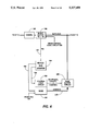
- the printing apparatus 10 comprises an image input terminal (IIT) 12, image output terminal (IOT) 14, a video processor (VP) 16 and an input/output coprocessor (IOCP) 300.
- IIT image input terminal
- IOT image output terminal
- VP video processor
- IOCP input/output coprocessor
- FIG. 2 the IIT 12, the IOT 14 and the VP 16 are shown in a digital copying apparatus.
- the concepts underlying the printing apparatus 10 are applicable to many types of machines employing a scanning device coupled with a printing or output device.
- the IIT 12 (FIG. 2) includes a scanning section having an automatic document handler (ADH) 20 for automatically and sequentially placing one or more documents 21 on a transparent platen 22.
- ADH automatic document handler
- the document 21 to be scanned is brought from a document tray 24 forward by the document handlers 26,27 into position on the platen 22 for scanning. Following scanning, the document 21 is returned to the document tray 24. While a particular document handler is shown, one skilled in the art will appreciate that other document handler types may be used instead or the documents 21 may be placed manually on the platen 22
- the scanning section of the IIT 12 employs one or more linear scanning arrays 30, which arrays 30 may comprise charge couple devices (CCDs) supported below and in scanning relation to the platen by a carriage 32.
- CCDs charge couple devices
- the carriage 32 can be reciprocated by reciprocating means 34, the reciprocating means 34 being similar to the reciprocating arrangement disclosed in U.S. Pat. No. 4,387,636 to Daniele et al., the pertinent portions of which patent are incorporated herein by reference.
- a suitable lens 36 is provided to focus arrays 30 on a line-like segment of the platen 22 and the documents resting thereon.
- a suitable lamp 38 illuminates the document line being scanned.
- arrays 30 provide electrical image data or pixels representative of the document image scanned which are inputted to the VP 16 across a suitable IIT interface 42.
- the image data may be used for purposes other than printing copies, as for example, the image data may be transmitted via a communication channel (not shown) to another location, or stored, etc.
- the interface 42 includes differential transmitters/receivers and appropriate control logic adapted to provide data/control flow between the IIT 12 and the VP 16.
- interface 42 provides for an 8 bit wide image data bus 44 having a constant transfer rate of 4 Mbytes/sec.
- Image data is transmitted from the VP 16--the structure and operation of which VP 16 is explained in further detail below--to the IOT 14 by way of an IOT interface 46. Additionally, the VP 16 is coupled with a input/output coprocessor (IOCP) 300, the structure and operation of which IOCP 300 is discussed in further detail below.
- IOCP input/output coprocessor
- the IOT 46 provides image data and control signal paths between the IOT 14 and the VP 16 as well as includes two two scan line deep ping-pong buffers (not shown), the ping-pong buffers preferably being two 2K ⁇ 8 SRAMs.
- the image data is clocked out of the IOT interface 46 by way of a byte clock (not shown).
- the IOT 14 includes a raster output scanner (ROS) 50 having a suitable source of high intensity light, such as laser 52, modulated in accordance with the content of the image data as by an acousto-optic modulator 54 to provide zero and first order imaging beams.
- the imaging beam is scanned across a photorecptor 56 at an exposing station 58 by a scanning polygon 60 to expose the previously charged photoreceptor 56 and create a latent electrostatic image or the document represented by the image signals to modulator 54.
- Suitable means (not shown) are employed to focus the beam on the photoreceptor 56.
- the printing apparatus 10 illustrated in FIG. 2 employs a removable processing cartridge 64 which may be inserted and withdrawn from the main machine frame in the direction of arrow 66.
- Cartridge 64 includes the photoreceptor 56, which in one example comprises a belt like member 68, the outer periphery of the belt like member 68 being coated with a suitable photoconductive material 70.
- the belt 68 is suitably mounted for revolution within the cartridge 64 about driven transport roll 72, around idler roll 74 and travels in the direction indicated by the arrows on the inner run of the belt to bring the image bearing surface thereon past the plurality of xerographic processing stations.
- Suitable drive means such as a motor, not shown, are provided to power and coordinate the motion of the various cooperating machine components whereby a faithful reproduction of the original input scene information is recorded upon a sheet of final support material 76, such as paper or the like.
- the belt 68 moves the photoconductive surface 70 through a charging station 78 wherein the belt 68 is uniformly charged with an electrostatic charge placed on the photoconductive surface 70 by charge corotron 80 in known manner preparatory to imaging. Thereafter, the belt 68 is driven to the exposure station 58 wherein the charged photoconductive surface 70 is exposed to line-by-line scanning of the ROS 50, whereby the charge is selectively dissipated in the light exposed regions to record the original input image in the form of electrostatic latent image.
- the speed of the scanning carriage 32 and the speed of the belt 68 are synchronized to provide faithful reproduction of the original document.
- the development station 82 includes a magnetic brush development system including developer roll 86 utilizing a magnetizable developer mix having course magnetic carrier granules and toner colorant particles.
- Sheets 76 of the final support material are supported in a stack arranged on elevated stack support tray 88. With the stack at its elevated position, the sheet separator segmented feed roll 90 feeds individual sheets therefrom to the registration pinch roll pair 92. The sheet 76 is then forwarded to a transfer station 94 in proper registration with the image on the belt and the developed image on the photoconductive surface 70 is brought into contact with the sheet 76 of final support material within the transfer station 94 and the toner image is transferred from the photoconductive surface 70 to the contacting side of the final support sheet 76 by means of transfer corotron 96.
- the final support material 76 is separated from the belt 68 by the beam strength of the support material 76 as it passes around the idler roll 74, and the sheet 76 containing the toner image thereon is advanced to fixing station 98 wherein roll fuser 100 fixes the transferred powder image thereto. After fusing the toner image to the sheet 76, it is advanced by output rolls 102 to sheet stacking tray 104.
- toner particles remaining on the photoconductive surface after the transfer operation are removed from the belt 70 by a cleaning station 108, which cleaning station 108 comprises a cleaning blade 110 in scrapping contact with the outer periphery of the belt 68 and contained within a cleaning housing 112, the cleaning housing 112 having a cleaning seal 114 associated with the upstream opening of the cleaning housing 112.
- the toner particles may be mechanically cleaned from the photoconductive surface by a cleaning brush as is well known in the art.
- the VP 16 comprises an input network 116, a first memory interface network 118, a memory network 120, a computer network 122 and a second memory interface network 124.
- the input network 116 comprises a multiplexor (MUX) 126 as well as a user interface (UI) 130 coupled with suitable UI logic circuitry 132.
- MUX multiplexor
- UI user interface
- a 16-bit bus 134 allows the MUX 126 and the UI logic circuitry 132 to communicate with the computer network 122.
- the 8-bit image data bus 44 communicates with the MUX 126 and the UI logic circuitry 132.
- the UI 130 includes conventional control circuitry coupled with a CRT, the control circuitry being adapted to initiate operation of the printing apparatus 10 in a known manner.
- the first memory interface network 118 which network 118 (FIG. 3) includes a compressor 138 coupled with the computer network 122 by suitable control logic circuit 140, a direct memory access (DMA) circuit 142, an image bus arbiter 144 and a burst buffer 146.
- the compressor 138 comprises conventional components of the type suitable for use with the adaptive algorithm disclosed in U.S. Pat. No. 4,559,563 (to Joiner, Jr.)("'563 patent"), the pertinent portions of which are incorporated herein by reference.
- the control logic 140 can comprise a known I/O device, such as the 8255 I/O port manufactured by Intel, Corp.
- One purpose of the compressor 138 is to maximize the rate at which data can be transmitted to the memory network 120. In the preferred form of operation, compression ratios of up to 30:1 have been achieved.
- the compressor 138 is coupled with the burst buffer 146 as an integrated adaptive compressor (IAC), the IAC being designated by the numeral 148.
- IAC integrated adaptive compressor
- the illustrated burst buffer 146 of FIG. 3 is a "first in/first out (FIFO)" type buffer having a capacity of 64 Bytes
- ping-pong buffers such as the ones used in the IOT interface 46, could be substituted for the FIFO burst buffer 146.
- 8 bit bytes inputted to the IAC 148 by way of bus 44 can be combined into 16 bit bytes for transmission to the memory section 120.
- the IAC 148 is interconnected with the DMA circuit 142 by a control line 150, and with the IBA 144 by way of a request line 152.
- Image data in the form of 16-bit bytes are transmitted through the memory network 120 by way of a 16 bit bi-directional image bus 154. Transmission of the image data from the IAC 148 is accomplished by use of the DMA circuit 142.
- the DMA circuit 142 includes a memory access register (MAR) 156 and a control logic circuit 158, the control logic circuit 158 being adapted to transfer image data to and from I/O components, such as the IAC 148.
- programming of the MAR 156 is achieved by use of the computer network 122, and more specifically with a CPU or MPU 160.
- the MAR 156 is packaged with control logic circuit 158, and the the MAR 156 (FIGS. 3 and 5) is coupled with the CPU 160 by way of a data bus 162 (PD00-PD15). Additionally, the MAR 156 and the control logic circuit 158 are coupled with the image bus arbiter 144 by way of respective control lines 163, 164.
- the memory network 120 includes a memory section 166 having a page buffer 168, the page buffer 168 being interconnected with the MAR 156 by a 24-bit address bus 170, and with the control logic circuit 158 by a control line 172.
- read, write and other appropriate page buffer control signals can be transmitted across the control line 172 in response to commands transmitted by the IBA 144 to the control logic circuit 158.
- the illustrated MAR 156 includes a first address counter 178 and a second address counter 180, both of which counters 178,180 are selectively coupled with the address bus 170 by way of a 2:1 MUX 181, the MUX 181 having a tri-stated output. Additionally, a first 24-bit preloadable comparator 182 and a second 24-bit preloadable comparator 184 are respectively coupled with the address counters 178,180. Each of the comparators 182,184 is adapted to set the beginning and finishing addresses of the address counter to which it is coupled.
- each of the counters 178, 180 and the comparators 182, 184 is coupled with an MPU interface 186, a control register 188, as well as a clock output and control logic circuit 190, by way of a suitable bus 192.
- the MPU interface 186 preferably comprises various control lines which permit control of the MAR 156 by the CPU 160.
- the four address lines PA1-PA4 can be used to set each internal register of the MAR 156, while the 16-bit bidirectional data bus lines of bus 162 can be used to provide control data for the control register 188.
- the control register 188 is divided into two sections, with one section being dedicated to the first counter 178, and the other section being dedicated to the second counter 180.
- the clock output and control logic circuit 190 which can provide a clock rate of up to 32 MHz, is adapted to select which of counters 178,180 is to be placed on the address bus 170 to count from one address to another.
- DRAM dynamic random access memory
- the page buffer 168 has 4 Mbytes of DRAM.
- DRAM is a relatively inexpensive alternative to static RAM.
- periodic refreshment is generally required by, for example, a conventional refresh control device (“RF controller") 196, which device 196 can be coupled with the page buffer 168 by way of the image data bus 154.
- the RF controller 196 communicates with the IBA 144 via request line 200, and with the control logic circuit 158 via a control line 202.
- a disk drive module 204 is disposed on the image data bus 154.
- the disk drive module 204 includes a disk drive 206, such as a "Winchester”-type hard disk drive with 50 Mbyte capacity, coupled with a disk drive controller ("DDC") 208. Further information regarding the structure and operation of the disk drive controller 208 is discussed in [Disk Drive Controller Application].
- the module 204 communicates with the page buffer 168 via the image data bus 154, as well as with the computer network 122 via the image bus 154 and an intermediate bus 210.
- the disk drive controller 208 is coupled with the IBA 144 by way of request line 212, and with control logic circuit 158 by way of control line 214.
- the second memory interface network 124 comprises a burst buffer 216, a decompressor 218 and an 8-bit raw data bypass bus 220.
- the burst buffer 216 is structurally equivalent to the burst buffer 146, and the decompressor 218 is part of the same IC package as the compressor 138.
- the burst buffer 216 is preferably coupled with the decompressor 218 to form an integrated adaptive decompressor (IAD) 222.
- IAD 222 is coupled with the IBA 144 by way of request line 224, and with control logic circuit 158 by way of control line 226.
- the output of the burst buffer 216 is preferably 8-bit and the decompressor 218 is on an 8-bit data bus 230.
- the output of the decompressor 184 can be transmitted to the IOT interface 46 for printing, in a known manner, at the ROS 50.
- the computer network 122 includes the CPU 160 coupled with a 16-bit CPU bus 232.
- the CPU 160 comprises a Motorola 68020 microprocessor capable of operating at a clock frequency of 10 MHz.
- the CPU bus 232 preferably comprises a 16-bit wide data bus, 23-bit wide address bus and control lines.
- Various types of memory namely a ROM device 234, a system RAM device 236 and an EEPROM device 238, are respectively coupled with the CPU bus 232 to support the CPU 160 in a known manner.
- a local interrupt and arbitration device 240 as well as a counter(s)/timers section 242 are coupled to the CPU bus 232 to facilitate management and operation of the CPU bus 232 in a known manner.
- an input device or data source 244 such as a workstation or another scanner can be coupled to the the CPU bus 232 so that data can be inputted to the memory section 166 concurrent with other I/O operations, such as accumulating image data in the burst buffer 146.
- a suitable interface is preferably employed to achieve suitable coupling.
- the CPU 160 can be interconnected with the IIT 12, by an IIT universal asynchronous receiving/transmitting (UART) device 246.
- UART universal asynchronous receiving/transmitting
- the CPU 160 as well as any device coupled to the bus 232, can use the CPU bus 232 and a request line 248 to seek access of the image data bus 154 through the IBA 144.
- the CPU 160 is coupled to the control logic circuit 158 by way of a control line 250.
- the CPU 160 represents the "brains" of the VP 16.
- the CPU 160 serves as an operating system for the VP 16 in that it is responsible for, among other things, system initialization, "housekeeping," system management and communication with I/O devices.
- the CPU 160 serves as a diagnostic tool for VP 16--transmitting diagnostic signals through the MUX 126 and receiving feedback signals across the buses 210, 232.
- the CPU 160 plays a major role in facilitating data transfer by way of its communication with the DMA 142 across data bus 162.
- the CPU 160 is capable of transferring data with the UI 130 and/or the page buffer 168 for manipulating image data.
- the CPU 160 has registers in which various known digital operations, such as resolution conversion and data rotation, can be performed on the image data.
- various known digital operations such as resolution conversion and data rotation
- the CPU 160 since the CPU 160 is in direct communication with the page buffer 168, by way of bus 210, the CPU 160 can transfer data with the page buffer 168 independent of the IAC 148. Consequently, data can be transferred directly between the page buffer 168 and the CPU 160 while image data is being accumulated in the burst buffer 146.
- each of the transceivers comprises a 74F245 bi-directional transceiver manufactured by Texas Instruments, Inc.
- the image data transmitted to IOT interface 46 from page buffer 168 can be printed, in a known manner, at IOT 14. Storing one or more pages of image data before printing, however, can cause some delay in printing. To eliminate such delay, the VP 16 is provided with a "direct data bus" 260, the bus 260 coupling the IIT interface 42 directly with the IOT interface 46. Accordingly, when the input rate of the IIT 12 is synchronized relative to the output rate of the IOT 14, line-by-line synchronous input/output operations can be achieved.
- the VP 16 is employed with an input/output coprocessor (IOCP), the IOCP being designated by the numeral 300 (FIG. 13) and discussed in further detail below.
- IOCP input/output coprocessor
- the IOCP 300 communicates with the VP 16 by way of an I/O bus 316, the I/O bus 316 being selectively coupled with the buses 154,232 (FIG. 3A) by way of an I/O interface 317.
- the IOCP 300 includes a CPU section 302 which, among other things, permits the IOCP 300 to selectively communicate with the VP 16 for seeking access to the bus 154.
- the CPU section 302 is interconnected with the control logic circuit 158 by a control line 304, and with the IBA 144 by way of a request line 306.
- the sequencing role of the IBA 144 can be more fully understood.
- the IBA 144 is implemented by way of a state machine, namely a Field Programmable Array, such as the PAL 82S105 manufactured by Signetics, Corporation. Referring to FIG. 6, the relationship of the IBA 144 to varios I/O components as well as to the control logic 158 and the page buffer 168, is shown.
- one or more of the IAC 148, the CPU 160, the RF controller 196, the disk drive controller (DDC) 208, the IAD 222 and the IOCP 300 transmit request signals across respective request lines 152, 248, 200, 212 and 224 and 306 to the IBA 144.
- the IBA 144 designates the order in which the above-mentioned components can access the bus 154. More specifically, the IBA 144 causes the control logic circuit 158 to transmit an appropriate control signal across one of control lines 150, 202, 214, 226 and 250 and 304 for selectively permitting one of the above-mentioned components to access the bus 154. As the control logic circuit 158 transmits the appropriate control signal to the designated one of the above-mentioned I/O components, it also transmits information to the page buffer 168, by way of control line 172, regarding which component has been permitted access to the bus 154. It will be appreciated by those in the art that while the sequencing arrangement has been shown with six components, in other contemplated embodiments additional components could be sequenced and controlled by the arrangement of the IBA 144 and the control logic circuit 158 without altering the concept disclosed by the present description.
- the concept underlying the software employed to implement the IBA 144 is discussed in further detail.
- the numbered "bubbles" represent states through which a state machine can pass.
- Programming of the PAL 82S105 to accomplish the software of FIG. 7 is known to those skilled in the art.
- the PAL of the IBA 144 is driven by a 25 MHz clock and all input signals are synchronized with the clock so that the arbitration time is less than 40 ns.
- the priorities of the devices coupled to the IBA 144 are assigned as follows:
- the priority of the RF 196 is fixed, while the priorities of the IAC 148, the IAD 222, the DDC 208, the CPU 160 and the IOCP 300 are rotated after each data transfer.
- the concept underlying the arbitration process is not affected by the order of priority in which the above-mentioned devices are set. Referring to FIG. 7, the sequencing and rotating capacity of the IBA 144 is explained in further detail.
- the machine checks to see if states 01-03 for the RF 196 are being executed. Assuming that the RF 196 is being serviced, the machine waits until the service routine for the RF 196 to be completed before proceeding to step 10 or 1D. Similarly, if the DDC 208, the CPU 160 or the IOCP 300 requests access to the bus 154, the machine determines whether the RF 196, the IAC 148 or the IAD 222 is being serviced before proceeding.
- the sequencing scheme of the arbitration example is elaborated on more completely in the Legend of FIG. 7.
- the rotation of the IAC 148 and IAD 222 as well as the rotation of the DDC 208, the CPU 160 and IOCP 300 is achieved by the setting of a "flag."
- a request arrives for the IAC 148 the machine proceeds from states 3F to 10 and sets a flag so that the priority of the IAC 148 is set below the priority of the IAD 222. Accordingly, after the process returns to state 3F, if requests are received from IAC 148 and IAD 196 within about the same preselected time interval, the process continues through states 1D-1A rather than 10-1A. Upon proceeding to state 1D, another flag is set so that the priorities of the IAC 148 and IAD 196 are again rotated.
- the same flag setting approach can be used in servicing the DDC 208, the CPU 160 and the IOCP 300.
- the exemplary process begins with the CPU 160 transferring data to the page buffer 168 (active). In the time interval between A and B, the RF 196, the IAC 148, the IAD 22 and the DDC 208 request access to the bus 154. The IBA 144 waits until the CPU 160 transfer is completed and then grants the bus 154 (at time B) to the device having the highest priority, i.e. the RF 196. The IAD 148 or the IAD 222 and the DDC 208 wait until RF 196 has completed its transfer.
- the DDC 208 After the DDC 208 has accessed the bus 154 (between times D and E), its priority is changed to less than #4 and at time E the CPU 160 accesses the bus 154. After the CPU 160 has made its second transfer (between times E and F), its priority is changed to less than #4 and the IOCP 300 accesses the bus 154 at time F. After the IOCP 300 has accessed the bus 154 (between times F and G), its priority is changed to #6 and the priorities of the DDC 208 and the CPU 160 are shifted back to #4 and #5, respectively. Accordingly, at time G, when a concurrent request for the bus 154 comes in from the DDC 208, the CPU 160 and the IOCP 300, access to the bus 154 is granted to the DDC 208.
- the printing apparatus 10 can be further understood by reference to the exemplary timing diagram FIG. 9. As will be appreciated by those skilled in the many modes of operation, other than the mode of operation discussed below, can be achieved with the various systems and subsystems of the printing apparatus 10 disclosed thus far.
- the parameters of the job such as number of prints to be made, size of each print, etc.
- the CPU 160 Prior to transmitting an appropriate scan signal to the scanning section of IIT 12 by way of the IIT UART 246, and a print signal to the IOT interface 46, the CPU 160 communicates with the MAR 156 (FIGS. 3 and 6), by way of data bus 162, to allow for the configuring of addresses in the page buffer 168, the addresses being the 24-bit locations at which image data are stored.
- the scan signal is transmitted to the scanning section of IIT 12.
- the corresponding image data is transmitted to the IAC 148, by way of the MUX 126, and to the IOT interface 46, by way of the direct data bus 260.
- each byte of image data transmitted to the IAC 148 is compressed, using the adaptive algorithm of U.S. Pat. No. 4,559,563, and temporarily accumulated in the burst buffer 146. As shown in FIG.
- image data can be written in or read from the page buffer 168 as image data is being accumulated in the burst buffer 146.
- FIGS. 4, 5 and 10 it will be understood how a byte of image data is written in the page buffer 168.
- the IAC 148 seeks access to the bus 154 through the IBA 144.
- the IBA 144 causes the control logic circuit 158 to synchronously transmit three signals to the IAC 148, the MAR 156 and the page buffer.
- the enabling signal, nAEN1 goes low and a valid address #1 is "pointed to" by the counter 178.
- the second signal which is transmitted across control line 150, allows the IAC 148 to access the bus 154 so that the image data byte is transferred to the designated address.
- the page buffer 168 stores the byte at the designated address.
- nAEN1 goes low, and the RDY signal goes low, the process can be repeated as many times as may be required to transfer a preselected group of bytes.
- the address counter 178 advances to the next address location in the page buffer 168 on the rising edge of nAEN1. If the data in the comparator 182 is equal to the count in the counter 178, CLR-C1 will go active active no later than 7.5 ns after the rising edge of the clock. CLR-C1 will stay active until the address in the counter 178 has been placed onto the output bus 170. Subsequently, when nAEN1 goes high, the counter 178 will be reset.
- DMA direct memory access
- up to eight (8) 16-bit bytes are accumulated in the burst buffer 146 of the IAC 148, and after buffering the eighth byte, four of the first-collected bytes are transferred to the page buffer 168 in the burst mode.
- a similar transfer scheme can be achieved for transferring image to and accumulating image data at the IAD 224.
- four bytes of image data can be transferred from the page buffer 168 to the burst buffer 216 of the IAD 222 in a burst mode for accumulation therein.
- the accumulated image data can be transferred to the IOT interface 46, by way of decompressor 218, at a rate that is substantially less than the burst mode transfer rate.
- components other than the IAC 148 and the IAD 222 can communicate with the page buffer 168 at time intervals in which image data is not being transferred to and from the page buffer 168 in the burst mode.
- FIG. 9 there are at least four intervals in which the page buffer 168 respectively communicates with the CPU 160, the RF 196, the DDC 208 and the IOCP 300 while image data is being accumulated at the burst buffer 146 and/or image data is being transmitted to the IOT interface 46.
- image data can be transmitted to the CPU 160 for manipulation thereof, and in another example image data can be stored sequentially in the disk drive 206 for subsequent printing. It will be recognized that use of the disk drive 206 to store image data is preferred when printing of sets of multiple copies is desired.
- image data can be transferred to/from the page buffer 168 from/to the IOCP 300.
- the compressor 138 can write image data to the burst buffer 146 at a rate of one (1) 16-bit byte per 700 ns
- the burst buffer 146 can accumulate four (4) 16-bit bytes in 2800 ns.
- the four bytes can be transferred to the page buffer 168 in 600 ns. Accordingly, during the accumulation period, 2200 ns remain for another I/O device to access the image data bus 154.
- image bus utilization of the image data bus 154 can be calculated relative to the I/O device using the bus 154 with the least frequency.
- the RF 196 having a refresh cycle of 300 ns every 15000 ns, requires the bus 154 with the least frequency, i.e. only 2% of the 15000 ns interval.
- the DDC 208 requests the bus once every 5000 ns (8% of the 15000 ns interval), and, for a worst case compression ratio of 1:1, either the IAC 148 or the IAD 222 requires a data transfer once every 2800 ns for 600 ns (8% of the 15000 ns interval).
- the CPU 160 can use the bus as much as 68.57% of the 15000 ns interval.
- compression rates which in the preferred embodiment can be as high as 30:1, even more bus access time is made available for either the CPU 160, the RF 196 and the DDC 208.
- the relatively high utilization scheme described above permits for advantageous operation of the printing apparatus 10 in that multiple functions, such as data transfer, data manipulation and data storage, can all be performed in a time interval that, at least to the user, seems extremely brief.
- some of the time given to the CPU 160 to use the bus 154 can be allocated to the IOCP 300 so that it too can access the bus 154 once every 2800 ns.
- each of counters or pointers 178,180 (FIG. 5) function as "loop-around pointers" whose movements are respectively limited by the pre-programmed comparators 180,182. Accordingly, respective movement of each of the counters or pointers 178,180 down the stack of the page buffer 168 is limited by the respective settings of the comparators 182,184. Such limiting of the pointers 178,180 is particularly suitable for those instances in which the user does not intend to overwrite certain data stored further down in the stack.
- Another aspect of the dual pointer arrangement is that image data need not be written into and read out of the page buffer 168 with the same counter.
- four bytes of image data have been written into the page buffer 168 from the IAC 148 so that the pointer 178 has been moved from the first address "A" to the fourth address "D.” If only pointer 178 were available, the image data would be read out of the page buffer 168 by looping the pointer 178 back to address A. With the concept disclosed by the present invention, however, the data at the addresses A-D can be read out using the second pointer 180.
- each of pointers 178,180 can be used to designate an address for use in any suitable page buffer operation.
- the address D can be designated for a data transfer operation with a first I/O device by causing the enabling signal nAEN1 to go low.
- the address at A can be designated for a data transfer operation with a second I/O device by causing the enabling signal nAEN2 to go low.
- the first I/O device could be the IAC 148 with image data being written into the page buffer 168
- the second I/O device could be the IAD 224 with data being read out to the IOT interface 46.
- the I/O devices could be various combinations of the IAC 148, the CPU 160, the RF 196, the DDC 208, the IAD 222 or any like I/O device that could be coupled with the page buffer 168.
- the IOCP 300 comprises the CPU section 302, Input/Output section 308, DMA 310, Input/Output Page Buffer (IOPB) 312 and Arbiter 314.
- the Input/Output Section 308 includes a plurality of discrete input/output modules, i.e. input/output cards (IOCs), each of which IOC is coupled with an I/O Bus 316 by way of a suitable connector 318.
- the I/O Bus 316 couples the IOCP 300 with the VP 16, via I/O interface 317, and is a multipurpose bus which is capable of concurrently transferring data, addresses and control signals.
- the I/O bus 316 can possess up to 16 data lines and 24 address lines.
- the I/O bus 316 is coupled with the buses 154,232 via the I/O interface 317, and the I/O bus 316 is coupled with an IOCP bus 322 by way of a transceiver or isolation amplifier 324.
- the dual bus system of the IOCP 300 serves to maximize the fault-tolerance of the IOCP 300. That is, through employment of seperate buses 316,322, the IOCs can communicate with the VP 16, even when the IOCP bus 322 is down, and the components coupled with the IOCP bus 322 can communicate among themselves, even when the I/O bus 316 is down.
- the discrete modules each of which includes a dedicated processor or a controller, are shown as a FAX 326, a local area network (LAN) module 328, a disk drive module 330, a communications port (COM) 332, a page description language (PDL)-decomposing (DEC) module 334 and an image manipulation board (IMB) 336.
- a host of other devices such as a floppy drive device, a keyboard/mouse or a CD ROM could be coupled to the I/O bus 316, as shown in U.S. Pat. No.
- the FAX 326 is a conventional group III type facsimile device, which may be similar in construction to the illustrated FAX of U.S. Pat. No. 5,021,892, the pertinent portions of which patent are incorporated herein by reference.
- the FAX 326 may include a transmission control portion (not shown), the control portion containing a slave CPU (not shown) for controlling a data transmission procedure based on a CCITT standard.
- the control portion is adapted to exchange data with the I/P bus 316 according to the transmission procedure.
- the control portion can also be connected to a telephone line by way of a modem (not shown) and a network control unit (not shown) as shown in the '892 patent.
- the LAN module 328 is shown in further detail.
- the LAN module 328 comprises a LAN system 348 and a controller 350 for interfacing the LAN system 348 with the I/O bus 316.
- the LAN system 348 includes an Ethernet LAN 349 to which a number of work stations 352 are connected.
- Workstation 352 may be, for example, the Xerox 6085 professional work stations.
- LAN 349 may also have other office connected equipment, such as a network file server 354, a network file mail communication server 356, a print server 358 and an electronic printer 360. Also, a large capacity remote storage facility, such as a mini-computer 362 may be connected to the LAN 349.
- the LAN system 348 is a collaborative system, meaning that it enables users at different workstations 352 to work together in real-time by processing and passing information among one another and storing and retrieving information from storage services 354 and 362 via the network 349.
- a fiber distributed data interface FDDI
- FDDI fiber distributed data interface
- the Disk Drive module 330 (FIG. 13) comprises one or more disk memory devices (not shown), which disk memory devices are coupled 7ith the I/O bus 316 by way of a disk drive controller 368, such as a SCSI controller.
- a disk drive controller 368 such as a SCSI controller.
- the general concepts underlying the structure and operation of the Disk Drive module 330 can be more fully appreciated by reference to FIGS. 3A, 3B and the accompanying discussion of the Disk Drive module 204.
- the communications port 332, which may, in one example, comprise a Centronics Port and/or a RS 232 allows various components of the IOCP 300 to communicate with peripherals, such as another terminal or printer.
- the PDL-DEC module 334 comprises all of the necessary hardware, such as a dedicated processor and suitable registers, to decompose a master PDL file into a bitmap file for printing.
- PDLs are an interchange standard for representing documents electronically within a system and ultimately printing those documents.
- documents formatted as a PDL file can be exchanged between the work stations 352 of the LAN system 348 and the PDL-DEC module 334 in an efficient and consistent manner.
- the PDL file describes, among other things, how images are to be rendered on each page, what font is to be employed and how the pages are to be assembled.
- the PDL-DEC module 334 can receive, as input for printing, electronic documents in various forms, such as POSTSCRIPT, HP-PCL or INTERPRESS.
- the image manipulation board (IMB) 336 comprises suitable hardware for achieving such functions as image editing and image conversion.
- the hardware may comprise a dedicated processor and a suitably sized bitmap, the bitmap being adapted for use with a large variety of software.
- the IMB 336 is particularly suited for, among other procedures, wide and small angle rotations, image annotation, or any other known image manipulation processes.
- the CPU section 302 which is coupled to the IOCP bus 322 by way of a transceiver 369, comprises a CPU 370, local DRAM 372, ROM/EPROM 374, Logic Section 376 and a Multi-Function Peripheral (MFP) 378, all of which are linked by a multipurpose local bus 380.
- the CPU 370 is an 8 MHz Motorola 68000 microprocessor which serves as a bus master for the local bus 380.
- the CPU 370 has all local, IOCP and I/O bus resources mapped to it, and is responsible for, among other things, performing diagnostics as well as implementing application software and the operating system of the IOCP 300.
- the EPROM 374 is sized at 32K or 64K, and contains power-up diagnostics and a boot program to download the local DRAM 372.
- the program and data for the CPU 370 is preferably provided by use of 512 KB of zero wait state DRAM. All of the suitable logic that permits the CPU 370 to control IOCP resources, handle interrupts and decode addresses resides in the Logic Section 376. Incoming interrupts are funneled into the MFP 378, which, in one example, is a Motorola 68901 IC.
- the 68901 includes a serial debug port, which port communicates with the VP 16 by way of line 381. Through use of the debug port and line 381, redundant emergency communication between the VP 16 and the IOCP 300 can be achieved during normal operation of the printing apparatus 10.
- the DMA 310 which is coupled to the IOCP bus 322 by way of a transceiver 382, comprises a DMA controller (DMAC) 384 and logic section 386.
- the DMAC 384 is an 8 Mhz Siemans 82257 IC possessing a four channel intelligent data transfer engine that enables transfers between the IOCs of the Input/Output section 308 and the IOPB 312 or the IOPB 312 and itself.
- the DMAC 384 can perform either frequent or infrequent transfers that would be impractical to implement via the CPU 370. For maximum performance, the DMAC 384 has the ability to synchronize its transfers on a cycle by cycle basis with a given data source.
- the DMAC 384 can operate without further intervention, and can interrupt the CPU 370 when the DMA 310 transfer is finished.
- the Siemans 82257 IC is capable of enabling both double cycle (two cycles per data item moved) and single cycle transfers (one cycle per data item moved).
- the logic section 386 which functions in response to commands from the DMAC 384, is adapted to, among other things, move data and addresses to and from various components of the IOCP 300.
- the DMA circuit 142 discussed above, with its MAR 156 and control logic circuit 158 could be used to implement the DMA 310.
- the IOPB 312 is preferably a 2 MB DRAM, with an expanded capacity of 4 MB.
- the IOPB 312, which advantageously permits image buffering, is coupled to the IOCP bus 322 by way of a transceiver 388. Accordingly, the IOPB 312 serves to prevent a slow data producer from wasting resources of the VP 16. In particular, at least one page of image data can be stored in the IOPB 312, manipulated if necessary, and then sent to the VP 16 at a relatively high speed. Additionally, the IOPB 312 can be used as a message communications buffer between the software programs of the VP 16 and the IOCP 300. In the preferred embodiment, the IOPB 312 comprises 16 (or 32 in an expanded mode) 1 Mb memory chips and control logic.
- another IMB board 336 is coupled to the IOCP bus 322. It will be appreciated that a host of intelligent I/O modules, such as the ones described in further detail above, could be coupled to the IOCP bus 322 to further enhance its "data-crunching" capabilities.
- the arbiter 314 is similar in structure to the arbiter 144 discussed above. Referring to FIG. 15A-15B, a state diagram for the arbiter 314 is shown. In the preferred embodiment, the VP 16, the CPU 370 and the DMAC 384, are respectively assigned to the states designated as "WAIT 1,” “WAIT 2" AND WAIT 3,” respectively. To gain access to the buses 316,322 (FIG. 13), the components respectively transmit request signals across request lines 392-394.
- Each component seeking access to the buses 316,322 receives an acknowledge signal transmitted by one of lines 396-398, and accesses the buses 316,322. It will be appreciated by those skilled in the art that the round-robin scheme could be modified so that, for example, the CPU 370 would encounter effectively no delay in accessing the bus 316 on account of arbitration. Referring to FIG.
- data is transferred to an IOC of the I/O section 308 from the IOPB 312 by first transmitting an address from the DMAC 384 to the IOPB 312 for retrieving data. The data is then transmitted with a corresponding address by the DMAC 384 to a port of the IOC. Once the address is decoded with a suitable decoder 400, the data is read into the IOC.
- the DMAC 384 places an address on the address bus and, while the address is valid (FIG.
- the IOPB 312 is preferably DRAM and requires periodic refreshing. Since refreshing should not be delayed, whenever a refresh signal (“REF") is received by the arbiter 314, a refresh cycle is performed (FIG. 15B) as soon as VP 16, CPU 370 and DMAC 384 are respectively in WAIT 1, WAIT 2 or WAIT 3.
- the signals RASEN and "REFACK” are asserted in states “REF 0" and "REF 3,” while the signals RASEN, CASEN and REFACK are asserted in states “REF 1" and "REF 2.”
- the DRAM has internal refresh counters which are enabled by use of the CAS before RAS refresh cycle of FIG. 15B.
- the IOCP 300 is capable of performing various internal tasks and communicating with the VP 16. Referring to FIG. 17, two examples of operation will be discussed in some detail.
- data is received at one of the IOCs of the input/output section 308, and an interrupt signal is transmitted accordingly to the MFP 378.
- data from the IOC is transmitted to the IOPB 312 by use of the CPU 370 or the DMA 310, and the CPU 370 then requests access to the bus 154, by way of the request line 306.
- the DMAC 384 is programmed by the CPU 370 to transfer the data to the page buffer 168.
- an acknowledge signal is transmitted to the logic section 376, by way of line 304, so that the control logic 386 can cause the data to be transferred from the IOPB 312 to the page buffer 168 in a burst mode.
- the data can be accumulated at a relatively slow rate in the IOPB 312 without impairing the operation of the VP 16, and, when the VP 16 is ready for the data from the IOPB 312, the data can be transferred at a relatively fast rate so that the VP 16 is not occupied by the relatively slow data rate transfer of the IOC.
- the VP 16 seeks access to the buses 316,322 by way of request line 392.
- the DMA 142 is programmed by the CPU 160 to transfer the data to the IOPB 312.
- an acknowledge signal is transmitted across line 396 to the VP 16 and the data is transferred to the IOPB 312 in a burst mode by use of the control logic 158.
- the data Once the data has been transferred to the IOPB 312, it can be transferred to an appropriate IOC at a rate that is considerably slower than the burst mode rate.
- the data can be transferred to the IOCP 300 at a relatively high rate so that the operation of the VP 16 is not unduly occupied with transferring the data to one of the IOCs, the IOCs tending to possess a relatively slow data transfer rate.
- IOCP 300 has only been described by way of two examples, those skilled in the art will appreciate the many uses to which the above-described IOCP 300 can be put. For instance while one of the above transfers is being performed, image manipulation can be achieved in either of the IMBs 336. Moreover, since each of the IOCs has its own controller or processor, many operations can be performed within the IOCs while the above transfers are being achieved. Finally, while the DMA 310 is in control of the buses 316,322, the CPU 160 can internally perform a wide variety of tasks.
Abstract
Description
______________________________________ RF 196 #1IAC 148IAD 222 #2/#3IAD 222 #2/#3DDC 208 #4/#5/#6CPU 160 #4/#5/#6IOCP 300 #4/#5/#6 ______________________________________
______________________________________ CPU 160 400 ns/16-bit byte (at 10 MHz clock)RF 196 400 ns/16-bit byte DDC 208 300 ns/Refresh Cycle ______________________________________
______________________________________ INPUTS, OUTPUTS, EQUATIONS AND REGISTER VALUES FOR STATE DIAGRAM OFARBITER 314 ______________________________________ INPUTS R1 ←Request # 1 R2 ←Request # 2 R3 ←Request # 3 REF ← Refresh Request M ← Memory Request OUTPUTS G1 ←Grant # 1 G2 ←Grant # 2 G3 ←Grant # 3 REFACK ← Refresh Ack. For Memory RASEN ← RAS Enable For Memory CASEN ← CAS Enable For Memory EQUATIONS P(1,2) = R2 ##STR1## P(1,3) = ##STR2## ##STR3## P(2,1) = ##STR4## ##STR5## P(2,3) = R3 ##STR6## P(3,1) = R1 ##STR7## P(3,2) = ##STR8## ##STR9## LA1 = ##STR10## ##STR11## LA2 = ##STR12## ##STR13## LA3 = ##STR14## ##STR15## NLA1 = (R2 + R3) ##STR16## NLA2 = (R1 + R3) ##STR17## NLA3 = (R1 + R2) ##STR18## ______________________________________
Claims (2)
Priority Applications (5)
| Application Number | Priority Date | Filing Date | Title |
|---|---|---|---|
| US07/812,314 US5307458A (en) | 1991-12-23 | 1991-12-23 | Input/output coprocessor for printing machine |
| JP33762592A JP3422505B2 (en) | 1991-12-23 | 1992-12-17 | I / O coprocessor for printing press |
| EP92311713A EP0552565B1 (en) | 1991-12-23 | 1992-12-22 | Input/output coprocessor for printing machine |
| DE69229992T DE69229992T2 (en) | 1991-12-23 | 1992-12-22 | I / O additional processor for a printer |
| US08/190,387 US5349647A (en) | 1991-12-23 | 1994-02-02 | Input/output coprocessor for printing machine |
Applications Claiming Priority (1)
| Application Number | Priority Date | Filing Date | Title |
|---|---|---|---|
| US07/812,314 US5307458A (en) | 1991-12-23 | 1991-12-23 | Input/output coprocessor for printing machine |
Related Child Applications (1)
| Application Number | Title | Priority Date | Filing Date |
|---|---|---|---|
| US08/190,387 Division US5349647A (en) | 1991-12-23 | 1994-02-02 | Input/output coprocessor for printing machine |
Publications (1)
| Publication Number | Publication Date |
|---|---|
| US5307458A true US5307458A (en) | 1994-04-26 |
Family
ID=25209194
Family Applications (2)
| Application Number | Title | Priority Date | Filing Date |
|---|---|---|---|
| US07/812,314 Expired - Lifetime US5307458A (en) | 1991-12-23 | 1991-12-23 | Input/output coprocessor for printing machine |
| US08/190,387 Expired - Fee Related US5349647A (en) | 1991-12-23 | 1994-02-02 | Input/output coprocessor for printing machine |
Family Applications After (1)
| Application Number | Title | Priority Date | Filing Date |
|---|---|---|---|
| US08/190,387 Expired - Fee Related US5349647A (en) | 1991-12-23 | 1994-02-02 | Input/output coprocessor for printing machine |
Country Status (4)
| Country | Link |
|---|---|
| US (2) | US5307458A (en) |
| EP (1) | EP0552565B1 (en) |
| JP (1) | JP3422505B2 (en) |
| DE (1) | DE69229992T2 (en) |
Cited By (37)
| Publication number | Priority date | Publication date | Assignee | Title |
|---|---|---|---|---|
| US5420696A (en) * | 1993-06-24 | 1995-05-30 | Xerox Corporation | Image data transfer architecture and method for an electronic reprographic machine |
| US5502797A (en) * | 1994-10-04 | 1996-03-26 | Lexmark International, Inc. | Apparatus with flash memory control for revision |
| EP0705023A2 (en) | 1994-09-29 | 1996-04-03 | Xerox Corporation | Apparatus and method for maximizing a rate of image data transfer in a printing system |
| US5553202A (en) * | 1992-03-19 | 1996-09-03 | Seiko Epson Corporation | Accessory control device which transfers data from electronic device using part of address signal and latch |
| US5579452A (en) * | 1994-09-29 | 1996-11-26 | Xerox Corporation | Method of managing memory allocation in a printing system |
| US5579453A (en) * | 1994-12-16 | 1996-11-26 | Xerox Corporation | Smart direct memory access controller |
| US5600762A (en) * | 1994-09-29 | 1997-02-04 | Xerox Corporation | Method of processing a job, in a printing system, with a composite job ticket |
| US5619649A (en) * | 1995-06-12 | 1997-04-08 | Xerox Corporation | Network printing system for programming a print job by selecting a job ticket identifier associated with remotely stored predefined document processing control instructions |
| US5659634A (en) * | 1994-09-29 | 1997-08-19 | Xerox Corporation | Apparatus and method for encoding and reconstructing image data |
| US5682467A (en) * | 1994-09-29 | 1997-10-28 | Xerox Corporation | Arbitrating apparatus for controlling selective access of multiple bus masters to a printing system video bus |
| US5687297A (en) * | 1995-06-29 | 1997-11-11 | Xerox Corporation | Multifunctional apparatus for appearance tuning and resolution reconstruction of digital images |
| US5697040A (en) * | 1996-07-10 | 1997-12-09 | Xerox Corporation | Print job intermixing within marking machine |
| US5740338A (en) * | 1995-11-13 | 1998-04-14 | Varis Corporation | Method for merging variable image data into a template image |
| US5778183A (en) * | 1995-06-12 | 1998-07-07 | Xerox Corporation | Apparatus and method of automatically transmitting event-related information to a user of a network printing system |
| US5835788A (en) * | 1996-09-18 | 1998-11-10 | Electronics For Imaging | System for transferring input/output data independently through an input/output bus interface in response to programmable instructions stored in a program memory |
| US5884015A (en) * | 1993-10-01 | 1999-03-16 | Canon Kabushiki Kaisha | Image forming apparatus for plural scanning |
| US5920685A (en) * | 1994-09-29 | 1999-07-06 | Xerox Corporation | Printing machine with merging/annotating/signaturizing capability |
| US6097499A (en) * | 1997-11-14 | 2000-08-01 | Lexmark International, Inc. | Methods and apparatus for isochronous printing with minimal buffering |
| US6266153B1 (en) | 1998-05-12 | 2001-07-24 | Xerox Corporation | Image forming device having a reduced toner consumption mode |
| US6286059B1 (en) * | 1993-12-29 | 2001-09-04 | Canon Kabushiki Kaisha | Information processing system displaying a selection state of a plurality of devices at the devices by a respective plurality of selection circuits |
| US6401143B1 (en) | 1999-12-02 | 2002-06-04 | Xerox Corporation | Loopback direct memory access control system for a digital scanner |
| US6463481B1 (en) | 1999-12-02 | 2002-10-08 | Xerox Corporation | Direct memory access control system for a digital scanner |
| US6501559B1 (en) | 1999-11-29 | 2002-12-31 | Xerox Corporation | Method and apparatus for managing job contention for system resources in an electronic reprographic system |
| US6570670B1 (en) | 1999-11-29 | 2003-05-27 | Xerox Corporation | Method and apparatus to enable job streaming for a set of commonly shared resources |
| US20030103225A1 (en) * | 2001-10-16 | 2003-06-05 | Keiichiro Hyodo | Interleaving imaging device controller with multi-use circuitry |
| US6614542B1 (en) | 1999-11-29 | 2003-09-02 | Xerox Corporation | Method and apparatus to improve system concurrency for a job using a set of commonly shared resources such that a specific resource is used only for a portion of the job |
| US6651081B1 (en) | 1999-11-29 | 2003-11-18 | Xerox Corporation | Method and apparatus for processing a high priority resource request in a system using a set of shared resources |
| US6665098B1 (en) | 2000-02-28 | 2003-12-16 | Xerox Corporation | Dynamic user interface based on frequency of user settings |
| US6671065B1 (en) | 1999-11-29 | 2003-12-30 | Xerox Corporation | Method and apparatus to optimize transition of resources from a lower priority to a higher priority job |
| US20040042668A1 (en) * | 2002-08-27 | 2004-03-04 | Michael Kaplinsky | CMOS image sensor apparatus with on-chip real-time pipelined JPEG compression module |
| US6717690B1 (en) | 1999-11-29 | 2004-04-06 | Xerox Corporation | Method and apparatus for managing job contention for system resources in an electrographic reproduction system where images are multibanded |
| US6738158B1 (en) | 1999-12-02 | 2004-05-18 | Xerox Corporation | Digital scanner for capturing and processing images |
| US20040130752A1 (en) * | 1995-01-18 | 2004-07-08 | Tesseron, Ltd. | Method of utilizing variable data fields with a page description language |
| US6762857B1 (en) | 1999-11-29 | 2004-07-13 | Xerox Corporation | Method and apparatus to enable processing multiple capabilities for a sub-job when using a set of commonly shared resources |
| US20050286065A1 (en) * | 1997-07-18 | 2005-12-29 | Gauthier Forrest P | Method and system for flowing data to an arbitrary path defined by a page description language |
| US20060200608A1 (en) * | 2004-11-30 | 2006-09-07 | Shih-Wei Peng | Bus arbiter and bus arbitrating method |
| US20080018935A1 (en) * | 1995-01-18 | 2008-01-24 | Gauthier Forrest P | Method and system for merging variable text and images into bitmaps defined by a page description language |
Families Citing this family (16)
| Publication number | Priority date | Publication date | Assignee | Title |
|---|---|---|---|---|
| US6292202B1 (en) * | 1993-07-29 | 2001-09-18 | Canon Kabushiki Kaisha | Image processing method and apparatus for hardware processing image data received from a device using software processing |
| US5619624A (en) * | 1994-05-20 | 1997-04-08 | Management Graphics, Inc. | Apparatus for selecting a rasterizer processing order for a plurality of graphic image files |
| US5493635A (en) * | 1994-06-14 | 1996-02-20 | Xerox Corporation | System for combining heterogeneous image processing jobs into a single job |
| US5758037A (en) * | 1994-10-25 | 1998-05-26 | Hewlett-Packard Company | Print controller with simplified video data processing |
| JPH08163338A (en) * | 1994-11-30 | 1996-06-21 | Ricoh Co Ltd | Image communication equipment |
| US5655138A (en) * | 1995-04-11 | 1997-08-05 | Elonex I. P. Holdings | Apparatus and method for peripheral device control with integrated data compression |
| JPH098989A (en) * | 1995-06-19 | 1997-01-10 | Brother Ind Ltd | Parallel data transfer system and electronic device |
| US5706409A (en) * | 1996-07-01 | 1998-01-06 | Xerox Corporation | Image shifting system for use in a document processing system |
| US6269190B1 (en) * | 1996-09-24 | 2001-07-31 | Electronics For Imaging, Inc. | Computer system for processing images using a virtual frame buffer |
| US5995724A (en) * | 1996-11-01 | 1999-11-30 | Mikkelsen; Carl | Image process system and process using personalization techniques |
| JPH10187600A (en) * | 1996-12-26 | 1998-07-21 | Canon Inc | Bus arbiter |
| US5971632A (en) | 1997-02-19 | 1999-10-26 | The Standard Register Company | Printer with internal document data construction |
| TW406229B (en) | 1997-11-06 | 2000-09-21 | Hitachi Ltd | Data process system and microcomputer |
| TW567695B (en) * | 2001-01-17 | 2003-12-21 | Ibm | Digital baseband system |
| AU2002351525A1 (en) * | 2001-06-28 | 2003-03-03 | Oak Technology, Inc. | System-on-a-chip controller |
| JP2016111633A (en) * | 2014-12-09 | 2016-06-20 | キヤノン株式会社 | Device having circuit capable of constructing logic circuit in accordance with circuit information and information processing system having a plurality of control means |
Citations (20)
| Publication number | Priority date | Publication date | Assignee | Title |
|---|---|---|---|---|
| US4169275A (en) * | 1977-03-10 | 1979-09-25 | Xerox Corporation | Reproduction scanning system having intermediate storage between input and output scanning stations |
| US4205350A (en) * | 1977-03-10 | 1980-05-27 | Xerox Corporation | Reproduction scanning system having intermediate storage between input and output scanning stations |
| US4580171A (en) * | 1981-05-01 | 1986-04-01 | Canon Kabushiki Kaisha | Image processing method and system |
| US4672186A (en) * | 1981-10-01 | 1987-06-09 | Banctec Inc. | Digital document scanning system |
| US4800431A (en) * | 1984-03-19 | 1989-01-24 | Schlumberger Systems And Services, Inc. | Video stream processing frame buffer controller |
| US4833596A (en) * | 1985-02-28 | 1989-05-23 | International Business Machines Corporation | Logical arrangement for controlling use of different system displays by main processor and co-processor |
| US4897735A (en) * | 1987-10-28 | 1990-01-30 | Ricoh Company, Ltd. | Image processing apparatus for multi-media copying machine |
| US4920481A (en) * | 1986-04-28 | 1990-04-24 | Xerox Corporation | Emulation with display update trapping |
| US4920427A (en) * | 1984-12-21 | 1990-04-24 | Kabushiki Kaisha Toshiba | Facsimile apparatus |
| US4931984A (en) * | 1987-07-31 | 1990-06-05 | Ricoh Company, Ltd. | File data retrieving system using retrieval-use-image data |
| US4987529A (en) * | 1988-08-11 | 1991-01-22 | Ast Research, Inc. | Shared memory bus system for arbitrating access control among contending memory refresh circuits, peripheral controllers, and bus masters |
| US5016114A (en) * | 1986-12-09 | 1991-05-14 | Ricoh Company, Ltd. | Digital copier apparatus with external laser card storage medium and image compression variable with available memory |
| US5021892A (en) * | 1986-09-30 | 1991-06-04 | Sharp Kabushiki Kaisha | Image processing device of multifunctional type |
| US5027221A (en) * | 1990-10-10 | 1991-06-25 | Fuji Xerox Co., Ltd. | Digital image recording system with preset control for selecting output formats based on the selected amount of pixel color and density data |
| US5038218A (en) * | 1990-10-10 | 1991-08-06 | Fuji Xerox Co., Ltd. | Image processing assembly with conversion and rotation of input image data or predetermined data to match data resolution and orientation |
| US5130809A (en) * | 1991-05-06 | 1992-07-14 | Fuji Xerox Co., Ltd. | Electrophotographic copier with constant rate data compression and simultaneous storage and decompression of compressed data received on a mutually coupled data bus |
| US5142667A (en) * | 1990-09-28 | 1992-08-25 | Xerox Corporation | Resource and memory management algorithms for electric printing and electronic reprographic systems |
| US5170466A (en) * | 1989-10-10 | 1992-12-08 | Unisys Corporation | Storage/retrieval system for document |
| US5170263A (en) * | 1990-10-10 | 1992-12-08 | Fuji Xerox Co., Ltd. | Image processing system |
| US5223948A (en) * | 1990-10-10 | 1993-06-29 | Fuji Xerox Co., Ltd. | Image processing apparatus |
Family Cites Families (3)
| Publication number | Priority date | Publication date | Assignee | Title |
|---|---|---|---|---|
| US4706126A (en) * | 1984-11-02 | 1987-11-10 | Ricoh Company. Ltd. | Facsimile apparatus |
| US4803617A (en) * | 1986-02-10 | 1989-02-07 | Eastman Kodak Company | Multi-processor using shared buses |
| US5155822A (en) * | 1987-08-13 | 1992-10-13 | Digital Equipment Corporation | High performance graphics workstation |
-
1991
- 1991-12-23 US US07/812,314 patent/US5307458A/en not_active Expired - Lifetime
-
1992
- 1992-12-17 JP JP33762592A patent/JP3422505B2/en not_active Expired - Fee Related
- 1992-12-22 EP EP92311713A patent/EP0552565B1/en not_active Expired - Lifetime
- 1992-12-22 DE DE69229992T patent/DE69229992T2/en not_active Expired - Fee Related
-
1994
- 1994-02-02 US US08/190,387 patent/US5349647A/en not_active Expired - Fee Related
Patent Citations (20)
| Publication number | Priority date | Publication date | Assignee | Title |
|---|---|---|---|---|
| US4205350A (en) * | 1977-03-10 | 1980-05-27 | Xerox Corporation | Reproduction scanning system having intermediate storage between input and output scanning stations |
| US4169275A (en) * | 1977-03-10 | 1979-09-25 | Xerox Corporation | Reproduction scanning system having intermediate storage between input and output scanning stations |
| US4580171A (en) * | 1981-05-01 | 1986-04-01 | Canon Kabushiki Kaisha | Image processing method and system |
| US4672186A (en) * | 1981-10-01 | 1987-06-09 | Banctec Inc. | Digital document scanning system |
| US4800431A (en) * | 1984-03-19 | 1989-01-24 | Schlumberger Systems And Services, Inc. | Video stream processing frame buffer controller |
| US4920427A (en) * | 1984-12-21 | 1990-04-24 | Kabushiki Kaisha Toshiba | Facsimile apparatus |
| US4833596A (en) * | 1985-02-28 | 1989-05-23 | International Business Machines Corporation | Logical arrangement for controlling use of different system displays by main processor and co-processor |
| US4920481A (en) * | 1986-04-28 | 1990-04-24 | Xerox Corporation | Emulation with display update trapping |
| US5021892A (en) * | 1986-09-30 | 1991-06-04 | Sharp Kabushiki Kaisha | Image processing device of multifunctional type |
| US5016114A (en) * | 1986-12-09 | 1991-05-14 | Ricoh Company, Ltd. | Digital copier apparatus with external laser card storage medium and image compression variable with available memory |
| US4931984A (en) * | 1987-07-31 | 1990-06-05 | Ricoh Company, Ltd. | File data retrieving system using retrieval-use-image data |
| US4897735A (en) * | 1987-10-28 | 1990-01-30 | Ricoh Company, Ltd. | Image processing apparatus for multi-media copying machine |
| US4987529A (en) * | 1988-08-11 | 1991-01-22 | Ast Research, Inc. | Shared memory bus system for arbitrating access control among contending memory refresh circuits, peripheral controllers, and bus masters |
| US5170466A (en) * | 1989-10-10 | 1992-12-08 | Unisys Corporation | Storage/retrieval system for document |
| US5142667A (en) * | 1990-09-28 | 1992-08-25 | Xerox Corporation | Resource and memory management algorithms for electric printing and electronic reprographic systems |
| US5027221A (en) * | 1990-10-10 | 1991-06-25 | Fuji Xerox Co., Ltd. | Digital image recording system with preset control for selecting output formats based on the selected amount of pixel color and density data |
| US5038218A (en) * | 1990-10-10 | 1991-08-06 | Fuji Xerox Co., Ltd. | Image processing assembly with conversion and rotation of input image data or predetermined data to match data resolution and orientation |
| US5170263A (en) * | 1990-10-10 | 1992-12-08 | Fuji Xerox Co., Ltd. | Image processing system |
| US5223948A (en) * | 1990-10-10 | 1993-06-29 | Fuji Xerox Co., Ltd. | Image processing apparatus |
| US5130809A (en) * | 1991-05-06 | 1992-07-14 | Fuji Xerox Co., Ltd. | Electrophotographic copier with constant rate data compression and simultaneous storage and decompression of compressed data received on a mutually coupled data bus |
Non-Patent Citations (2)
| Title |
|---|
| Research Disclosure Mar. 1991, 32388, Reproduction Apparatus Providing User Manual and Other Documentation, pp. 201 203. * |
| Research Disclosure Mar. 1991, 32388, Reproduction Apparatus Providing User Manual and Other Documentation, pp. 201-203. |
Cited By (46)
| Publication number | Priority date | Publication date | Assignee | Title |
|---|---|---|---|---|
| US5553202A (en) * | 1992-03-19 | 1996-09-03 | Seiko Epson Corporation | Accessory control device which transfers data from electronic device using part of address signal and latch |
| US5420696A (en) * | 1993-06-24 | 1995-05-30 | Xerox Corporation | Image data transfer architecture and method for an electronic reprographic machine |
| US5884015A (en) * | 1993-10-01 | 1999-03-16 | Canon Kabushiki Kaisha | Image forming apparatus for plural scanning |
| US6286059B1 (en) * | 1993-12-29 | 2001-09-04 | Canon Kabushiki Kaisha | Information processing system displaying a selection state of a plurality of devices at the devices by a respective plurality of selection circuits |
| US5717842A (en) * | 1994-09-29 | 1998-02-10 | Xerox Corporation | Method of managing memory allocation in a printing system |
| US5920685A (en) * | 1994-09-29 | 1999-07-06 | Xerox Corporation | Printing machine with merging/annotating/signaturizing capability |
| EP0705023A2 (en) | 1994-09-29 | 1996-04-03 | Xerox Corporation | Apparatus and method for maximizing a rate of image data transfer in a printing system |
| US5600762A (en) * | 1994-09-29 | 1997-02-04 | Xerox Corporation | Method of processing a job, in a printing system, with a composite job ticket |
| US5579452A (en) * | 1994-09-29 | 1996-11-26 | Xerox Corporation | Method of managing memory allocation in a printing system |
| US5659634A (en) * | 1994-09-29 | 1997-08-19 | Xerox Corporation | Apparatus and method for encoding and reconstructing image data |
| US5682467A (en) * | 1994-09-29 | 1997-10-28 | Xerox Corporation | Arbitrating apparatus for controlling selective access of multiple bus masters to a printing system video bus |
| EP0705023A3 (en) * | 1994-09-29 | 1996-06-05 | Xerox Corp | Apparatus and method for maximizing a rate of image data transfer in a printing system |
| US5710873A (en) * | 1994-09-29 | 1998-01-20 | Xerox Corporation | Apparatus and method for maximizing a rate of image data transfer in a printing system |
| US5502797A (en) * | 1994-10-04 | 1996-03-26 | Lexmark International, Inc. | Apparatus with flash memory control for revision |
| US5579453A (en) * | 1994-12-16 | 1996-11-26 | Xerox Corporation | Smart direct memory access controller |
| US20040130752A1 (en) * | 1995-01-18 | 2004-07-08 | Tesseron, Ltd. | Method of utilizing variable data fields with a page description language |
| US20040141197A1 (en) * | 1995-01-18 | 2004-07-22 | Tesseron, Ltd. | Method of utilizing variable data fields with a page description language |
| US20050185212A1 (en) * | 1995-01-18 | 2005-08-25 | Gauthier Forrest P. | Method of utilizing variable data fields with a page description language |
| US20080018935A1 (en) * | 1995-01-18 | 2008-01-24 | Gauthier Forrest P | Method and system for merging variable text and images into bitmaps defined by a page description language |
| US5778183A (en) * | 1995-06-12 | 1998-07-07 | Xerox Corporation | Apparatus and method of automatically transmitting event-related information to a user of a network printing system |
| US5619649A (en) * | 1995-06-12 | 1997-04-08 | Xerox Corporation | Network printing system for programming a print job by selecting a job ticket identifier associated with remotely stored predefined document processing control instructions |
| US5687297A (en) * | 1995-06-29 | 1997-11-11 | Xerox Corporation | Multifunctional apparatus for appearance tuning and resolution reconstruction of digital images |
| US5796930A (en) * | 1995-11-13 | 1998-08-18 | Varis Corporation | System architecture for processing and transporting page-map or bit-map data to a raster print engine |
| US5740338A (en) * | 1995-11-13 | 1998-04-14 | Varis Corporation | Method for merging variable image data into a template image |
| US5697040A (en) * | 1996-07-10 | 1997-12-09 | Xerox Corporation | Print job intermixing within marking machine |
| US5835788A (en) * | 1996-09-18 | 1998-11-10 | Electronics For Imaging | System for transferring input/output data independently through an input/output bus interface in response to programmable instructions stored in a program memory |
| US20050286065A1 (en) * | 1997-07-18 | 2005-12-29 | Gauthier Forrest P | Method and system for flowing data to an arbitrary path defined by a page description language |
| US6097499A (en) * | 1997-11-14 | 2000-08-01 | Lexmark International, Inc. | Methods and apparatus for isochronous printing with minimal buffering |
| US6266153B1 (en) | 1998-05-12 | 2001-07-24 | Xerox Corporation | Image forming device having a reduced toner consumption mode |
| US6570670B1 (en) | 1999-11-29 | 2003-05-27 | Xerox Corporation | Method and apparatus to enable job streaming for a set of commonly shared resources |
| US6651081B1 (en) | 1999-11-29 | 2003-11-18 | Xerox Corporation | Method and apparatus for processing a high priority resource request in a system using a set of shared resources |
| US6671065B1 (en) | 1999-11-29 | 2003-12-30 | Xerox Corporation | Method and apparatus to optimize transition of resources from a lower priority to a higher priority job |
| US6614542B1 (en) | 1999-11-29 | 2003-09-02 | Xerox Corporation | Method and apparatus to improve system concurrency for a job using a set of commonly shared resources such that a specific resource is used only for a portion of the job |
| US6717690B1 (en) | 1999-11-29 | 2004-04-06 | Xerox Corporation | Method and apparatus for managing job contention for system resources in an electrographic reproduction system where images are multibanded |
| US6762857B1 (en) | 1999-11-29 | 2004-07-13 | Xerox Corporation | Method and apparatus to enable processing multiple capabilities for a sub-job when using a set of commonly shared resources |
| US6501559B1 (en) | 1999-11-29 | 2002-12-31 | Xerox Corporation | Method and apparatus for managing job contention for system resources in an electronic reprographic system |
| US6738158B1 (en) | 1999-12-02 | 2004-05-18 | Xerox Corporation | Digital scanner for capturing and processing images |
| US6401143B1 (en) | 1999-12-02 | 2002-06-04 | Xerox Corporation | Loopback direct memory access control system for a digital scanner |
| US6463481B1 (en) | 1999-12-02 | 2002-10-08 | Xerox Corporation | Direct memory access control system for a digital scanner |
| US6665098B1 (en) | 2000-02-28 | 2003-12-16 | Xerox Corporation | Dynamic user interface based on frequency of user settings |
| US20030103225A1 (en) * | 2001-10-16 | 2003-06-05 | Keiichiro Hyodo | Interleaving imaging device controller with multi-use circuitry |
| US7821658B2 (en) * | 2001-10-16 | 2010-10-26 | Minolta Co., Ltd | Interleaving imaging device controller with multi-use circuitry |
| US20040042668A1 (en) * | 2002-08-27 | 2004-03-04 | Michael Kaplinsky | CMOS image sensor apparatus with on-chip real-time pipelined JPEG compression module |
| US20070097239A1 (en) * | 2002-08-27 | 2007-05-03 | Micron Technology, Inc. | CMOS image sensor apparatus with on-chip real-time pipelined JPEG compression module |
| US7532760B2 (en) * | 2002-08-27 | 2009-05-12 | Aptina Imaging Corporation | CMOS image sensor apparatus with on-chip real-time pipelined JPEG compression module |
| US20060200608A1 (en) * | 2004-11-30 | 2006-09-07 | Shih-Wei Peng | Bus arbiter and bus arbitrating method |
Also Published As
| Publication number | Publication date |
|---|---|
| DE69229992D1 (en) | 1999-10-21 |
| EP0552565A3 (en) | 1994-05-18 |
| JPH0670118A (en) | 1994-03-11 |
| JP3422505B2 (en) | 2003-06-30 |
| DE69229992T2 (en) | 2000-03-16 |
| EP0552565B1 (en) | 1999-09-15 |
| EP0552565A2 (en) | 1993-07-28 |
| US5349647A (en) | 1994-09-20 |
Similar Documents
| Publication | Publication Date | Title |
|---|---|---|
| US5307458A (en) | Input/output coprocessor for printing machine | |
| US5276799A (en) | Expandable electronic subsystem for a printing machine | |
| US5261047A (en) | Bus arbitration scheme for facilitating operation of a printing apparatus | |
| US5303341A (en) | Video processor for a printing apparatus | |
| US5717842A (en) | Method of managing memory allocation in a printing system | |
| US5920685A (en) | Printing machine with merging/annotating/signaturizing capability | |
| US7782480B2 (en) | Image forming apparatus | |
| US5710873A (en) | Apparatus and method for maximizing a rate of image data transfer in a printing system | |
| US5659634A (en) | Apparatus and method for encoding and reconstructing image data | |
| EP0733976A1 (en) | Chip select signal generator | |
| US5218456A (en) | Disk bandwidth allocations to prioritize disk requests | |
| US6337746B1 (en) | Interface card for coupling a computer to an external device | |
| US5894586A (en) | System for providing access to memory in which a second processing unit is allowed to access memory during a time slot assigned to a first processing unit | |
| US6449064B1 (en) | Method and apparatus for image formation that can handle simultaneously input data without causing a delay | |
| US5970222A (en) | Memory management system for printing a print job with limited capacity | |
| EP1104170A2 (en) | Method and apparatus for managing job contention for system resources in a electrographic reproduction system where images are multibanded | |
| EP1104168A2 (en) | Method and apparatus for managing job contention for system resources in an electronic reprographic system | |
| CA2156137C (en) | Programmable arbitrating apparatus | |
| US5495339A (en) | Scheduling multiple disk requests and writing data buffers to disk | |
| US7301653B2 (en) | Image processing apparatus, image processing method, and storage medium | |
| US6304927B1 (en) | Digital copier with scalable architecture | |
| JPH07105869B2 (en) | Input job processing method | |
| JPH06259204A (en) | Device and method for processing information | |
| JPH11146159A (en) | Image forming device | |
| JPH09146828A (en) | Memory controller and memory device |
Legal Events
| Date | Code | Title | Description |
|---|---|---|---|
| AS | Assignment |
Owner name: XEROX CORPORATION A CORPORATION OF NY, CONNECTI Free format text: ASSIGNMENT OF ASSIGNORS INTEREST.;ASSIGNORS:FREIBURG, JOSEPH A.;RIVSHIN, ISAAK;REEL/FRAME:005972/0200 Effective date: 19911218 |
|
| STCF | Information on status: patent grant |
Free format text: PATENTED CASE |
|
| FPAY | Fee payment |
Year of fee payment: 4 |
|
| FPAY | Fee payment |
Year of fee payment: 8 |
|
| AS | Assignment |
Owner name: BANK ONE, NA, AS ADMINISTRATIVE AGENT, ILLINOIS Free format text: SECURITY INTEREST;ASSIGNOR:XEROX CORPORATION;REEL/FRAME:013153/0001 Effective date: 20020621 |
|
| AS | Assignment |
Owner name: JPMORGAN CHASE BANK, AS COLLATERAL AGENT, TEXAS Free format text: SECURITY AGREEMENT;ASSIGNOR:XEROX CORPORATION;REEL/FRAME:015134/0476 Effective date: 20030625 Owner name: JPMORGAN CHASE BANK, AS COLLATERAL AGENT,TEXAS Free format text: SECURITY AGREEMENT;ASSIGNOR:XEROX CORPORATION;REEL/FRAME:015134/0476 Effective date: 20030625 |
|
| FPAY | Fee payment |
Year of fee payment: 12 |
|
| AS | Assignment |
Owner name: XEROX CORPORATION, CONNECTICUT Free format text: RELEASE BY SECURED PARTY;ASSIGNOR:JPMORGAN CHASE BANK, N.A. AS SUCCESSOR-IN-INTEREST ADMINISTRATIVE AGENT AND COLLATERAL AGENT TO JPMORGAN CHASE BANK;REEL/FRAME:066728/0193 Effective date: 20220822 |