US5283460A - Optical semiconductor device - Google Patents
Optical semiconductor device Download PDFInfo
- Publication number
- US5283460A US5283460A US07/834,611 US83461192A US5283460A US 5283460 A US5283460 A US 5283460A US 83461192 A US83461192 A US 83461192A US 5283460 A US5283460 A US 5283460A
- Authority
- US
- United States
- Prior art keywords
- area
- epitaxial layer
- substrate
- separating area
- conductivity type
- Prior art date
- Legal status (The legal status is an assumption and is not a legal conclusion. Google has not performed a legal analysis and makes no representation as to the accuracy of the status listed.)
- Expired - Lifetime
Links
- 239000004065 semiconductor Substances 0.000 title claims abstract description 61
- 230000003287 optical effect Effects 0.000 title claims abstract description 32
- 239000000758 substrate Substances 0.000 claims abstract description 89
- 239000000463 material Substances 0.000 claims abstract description 15
- 239000012535 impurity Substances 0.000 claims description 37
- 238000009792 diffusion process Methods 0.000 claims description 35
- 238000000034 method Methods 0.000 claims description 11
- ZOXJGFHDIHLPTG-UHFFFAOYSA-N Boron Chemical compound [B] ZOXJGFHDIHLPTG-UHFFFAOYSA-N 0.000 description 14
- 229910052796 boron Inorganic materials 0.000 description 14
- OAICVXFJPJFONN-UHFFFAOYSA-N Phosphorus Chemical compound [P] OAICVXFJPJFONN-UHFFFAOYSA-N 0.000 description 9
- 229910052698 phosphorus Inorganic materials 0.000 description 9
- 239000011574 phosphorus Substances 0.000 description 9
- 239000012528 membrane Substances 0.000 description 7
- 239000002243 precursor Substances 0.000 description 7
- 239000000969 carrier Substances 0.000 description 6
- 230000008569 process Effects 0.000 description 6
- XAGFODPZIPBFFR-UHFFFAOYSA-N aluminium Chemical compound [Al] XAGFODPZIPBFFR-UHFFFAOYSA-N 0.000 description 5
- 229910052782 aluminium Inorganic materials 0.000 description 5
- 125000004429 atom Chemical group 0.000 description 5
- 238000010438 heat treatment Methods 0.000 description 5
- 238000004519 manufacturing process Methods 0.000 description 5
- 230000015572 biosynthetic process Effects 0.000 description 4
- 229910052787 antimony Inorganic materials 0.000 description 3
- WATWJIUSRGPENY-UHFFFAOYSA-N antimony atom Chemical compound [Sb] WATWJIUSRGPENY-UHFFFAOYSA-N 0.000 description 3
- QVGXLLKOCUKJST-UHFFFAOYSA-N atomic oxygen Chemical compound [O] QVGXLLKOCUKJST-UHFFFAOYSA-N 0.000 description 3
- 230000007423 decrease Effects 0.000 description 3
- 238000005530 etching Methods 0.000 description 3
- 239000007789 gas Substances 0.000 description 3
- 238000002513 implantation Methods 0.000 description 3
- 229910052760 oxygen Inorganic materials 0.000 description 3
- 239000001301 oxygen Substances 0.000 description 3
- 230000004044 response Effects 0.000 description 3
- 238000007669 thermal treatment Methods 0.000 description 3
- XUIMIQQOPSSXEZ-UHFFFAOYSA-N Silicon Chemical compound [Si] XUIMIQQOPSSXEZ-UHFFFAOYSA-N 0.000 description 2
- 238000005468 ion implantation Methods 0.000 description 2
- 229920002120 photoresistant polymer Polymers 0.000 description 2
- 238000007740 vapor deposition Methods 0.000 description 2
- 229910000676 Si alloy Inorganic materials 0.000 description 1
- XMIJDTGORVPYLW-UHFFFAOYSA-N [SiH2] Chemical compound [SiH2] XMIJDTGORVPYLW-UHFFFAOYSA-N 0.000 description 1
- 238000010521 absorption reaction Methods 0.000 description 1
- CSDREXVUYHZDNP-UHFFFAOYSA-N alumanylidynesilicon Chemical compound [Al].[Si] CSDREXVUYHZDNP-UHFFFAOYSA-N 0.000 description 1
- 238000006243 chemical reaction Methods 0.000 description 1
- 239000011248 coating agent Substances 0.000 description 1
- 238000000576 coating method Methods 0.000 description 1
- 239000000356 contaminant Substances 0.000 description 1
- 238000011109 contamination Methods 0.000 description 1
- 230000000694 effects Effects 0.000 description 1
- 230000005684 electric field Effects 0.000 description 1
- 230000005672 electromagnetic field Effects 0.000 description 1
- 238000001704 evaporation Methods 0.000 description 1
- 230000008020 evaporation Effects 0.000 description 1
- BHEPBYXIRTUNPN-UHFFFAOYSA-N hydridophosphorus(.) (triplet) Chemical compound [PH] BHEPBYXIRTUNPN-UHFFFAOYSA-N 0.000 description 1
- 230000003993 interaction Effects 0.000 description 1
- 239000013067 intermediate product Substances 0.000 description 1
- 238000002955 isolation Methods 0.000 description 1
- 230000031700 light absorption Effects 0.000 description 1
- 210000003141 lower extremity Anatomy 0.000 description 1
- 238000012423 maintenance Methods 0.000 description 1
- 238000012986 modification Methods 0.000 description 1
- 230000004048 modification Effects 0.000 description 1
- 229910021421 monocrystalline silicon Inorganic materials 0.000 description 1
- 230000003071 parasitic effect Effects 0.000 description 1
- 230000002093 peripheral effect Effects 0.000 description 1
- 125000004437 phosphorous atom Chemical group 0.000 description 1
- 238000002360 preparation method Methods 0.000 description 1
- 239000000047 product Substances 0.000 description 1
- 229910052710 silicon Inorganic materials 0.000 description 1
- 239000010703 silicon Substances 0.000 description 1
- 238000004528 spin coating Methods 0.000 description 1
Images


Classifications
-
- H—ELECTRICITY
- H01—ELECTRIC ELEMENTS
- H01L—SEMICONDUCTOR DEVICES NOT COVERED BY CLASS H10
- H01L27/00—Devices consisting of a plurality of semiconductor or other solid-state components formed in or on a common substrate
- H01L27/14—Devices consisting of a plurality of semiconductor or other solid-state components formed in or on a common substrate including semiconductor components sensitive to infrared radiation, light, electromagnetic radiation of shorter wavelength or corpuscular radiation and specially adapted either for the conversion of the energy of such radiation into electrical energy or for the control of electrical energy by such radiation
- H01L27/144—Devices controlled by radiation
- H01L27/146—Imager structures
- H01L27/14683—Processes or apparatus peculiar to the manufacture or treatment of these devices or parts thereof
- H01L27/14689—MOS based technologies
-
- H—ELECTRICITY
- H01—ELECTRIC ELEMENTS
- H01L—SEMICONDUCTOR DEVICES NOT COVERED BY CLASS H10
- H01L27/00—Devices consisting of a plurality of semiconductor or other solid-state components formed in or on a common substrate
- H01L27/14—Devices consisting of a plurality of semiconductor or other solid-state components formed in or on a common substrate including semiconductor components sensitive to infrared radiation, light, electromagnetic radiation of shorter wavelength or corpuscular radiation and specially adapted either for the conversion of the energy of such radiation into electrical energy or for the control of electrical energy by such radiation
- H01L27/144—Devices controlled by radiation
- H01L27/146—Imager structures
-
- H—ELECTRICITY
- H01—ELECTRIC ELEMENTS
- H01L—SEMICONDUCTOR DEVICES NOT COVERED BY CLASS H10
- H01L27/00—Devices consisting of a plurality of semiconductor or other solid-state components formed in or on a common substrate
- H01L27/14—Devices consisting of a plurality of semiconductor or other solid-state components formed in or on a common substrate including semiconductor components sensitive to infrared radiation, light, electromagnetic radiation of shorter wavelength or corpuscular radiation and specially adapted either for the conversion of the energy of such radiation into electrical energy or for the control of electrical energy by such radiation
- H01L27/144—Devices controlled by radiation
- H01L27/1443—Devices controlled by radiation with at least one potential jump or surface barrier
-
- H—ELECTRICITY
- H01—ELECTRIC ELEMENTS
- H01L—SEMICONDUCTOR DEVICES NOT COVERED BY CLASS H10
- H01L27/00—Devices consisting of a plurality of semiconductor or other solid-state components formed in or on a common substrate
- H01L27/14—Devices consisting of a plurality of semiconductor or other solid-state components formed in or on a common substrate including semiconductor components sensitive to infrared radiation, light, electromagnetic radiation of shorter wavelength or corpuscular radiation and specially adapted either for the conversion of the energy of such radiation into electrical energy or for the control of electrical energy by such radiation
- H01L27/144—Devices controlled by radiation
- H01L27/146—Imager structures
- H01L27/14601—Structural or functional details thereof
- H01L27/1463—Pixel isolation structures
Definitions
- This invention relates to integrated circuits and, more specifically, to an optical semiconductor device having, integrally formed therein, a photo diode and a bipolar transistor.
- a monolithic optical semiconductor device integrally combining a light receiving element and a peripheral circuit, can be produced at a lower cost and is relatively immune to noise from external electromagnetic fields.
- a conventional optical semiconductor device is disclosed in, for example, Japanese Laid-open Patent Publication No. 1-205564.
- a P-type semiconductor substrate 1 has epitaxially grown thereon a P-type epitaxial layer 2.
- An N-type epitaxial layer 3 is epitaxially grown on epitaxial layer 2.
- a plurality of P + -type separating areas 4 separate epitaxial area 3, and contiguous upper portions of epitaxial layer 2 into isolated islands.
- a first island is used to form a photo diode 9.
- a second island is used to form an NPN transistor 10.
- Photo diode 9 includes an N + -type diffusion area in its upper surface.
- An N + -type buried layer 6 spans the interface between epitaxial layers 2 and 3 in the island forming transistor 10.
- the portion of epitaxial layer 3 in transistor 10 functions as the collector thereof.
- a P-type base area 7 is disposed in an upper surface of transistor 10.
- An N + -type N + -type emitter area is disposed in an upper surface of base area 7.
- An N + -type type collector contact area 12 is disposed in the upper surface of transistor 10 outside base area 7.
- Photo diode 9 is biased to form a PN junction between P-type epitaxial layer 2 and N-type epitaxial layer 3.
- N + -type diffusion area 5 serves as a cathode of photo diode 9.
- Separating area 4 serves as an anode of photo diode 9.
- An accelerated electric field is formed in NPN transistor 10 by an auto-doped layer 11 in epitaxial layer 2 which became autodoped by diffusion of P-type carriers from substrate 1 during epitaxial growth and heat treatment Autodoped layer 11 retards the movement of carriers originating below the depletion region.
- the depletion region is widened to restrain the movement of carriers occurring outside the depletion region.
- automatic doping layer 11 overlaps P-type epitaxial layer 2. This overlap results in an increased concentration of impurities and an enlargement of the depletion region.
- Epitaxial growth requires processing in a closed vessel into which gasses are fed to grow the desired layer, and to introduce the desired amount of impurities.
- the closed vessel becomes contaminated with the P-type impurities. If an attempt were made to grow N-type epitaxial layer 3 in the same closed vessel used to grow P-type epitaxial layer 2, the P-type contaminants in the vessel would enter epitaxial layer 3 in such amounts that it would be difficult or impossible to attain the desired properties in epitaxial layer 3.
- the device must be removed physically from the vessel after epitaxial layer 2 is formed, and placed in a clean vessel for growth of N-type epitaxial layer 3. This requirement for removing and reinstalling the workpiece during processing interferes with production. Thus, the same epitaxial growing device cannot be used to produce the prior-art device of FIG. 9.
- the present invention provides an optical semiconductor that includes a photo diode integrated with a transistor built on first and second epitaxial layers grown on a substrate, the first epitaxial layer is grown on the substrate from intrinsic material.
- the second epitaxial layer is grown doped on the first epitaxial layer.
- a separating area divides the optical semiconductor into first and second isolated islands.
- the separating area is made up of a lower separating area, a middle separating area and an upper separating area united to form a single separating area.
- the lower separating area is diffused at least upward from an interface between the substrate and the first epitaxial area.
- the middle separating area is diffused both downward and upward from an interface between the first and second epitaxial layers.
- the upper separating area is diffused downward from the surface of the second epitaxial layer.
- the photo diode is formed in the first island area, and the transistor is formed in the second island area.
- the separating area enters the substrate to a depth corresponding to the depth of the counterdoped region.
- an optical semiconductor device comprising: a semiconductor substrate of a first conductivity type, a first epitaxial layer epitaxially grown of intrinsic material on a surface of the semiconductor substrate, a second epitaxial layer of a reverse conductivity type epitaxially grown on a surface of the first epitaxial layer, a separating area of a second conductivity type dividing the first and second epitaxial layers into at least first and second island areas, the separating area including a lower separating area, a middle separating area and an upper separating area, all congruent and joined together, the lower separating area being diffused upward from a surface of the substrate, the upper separating area being diffused downward from a surface of the second epitaxial area, the middle separating area being centered in an interface between the first and second epitaxial layers, being diffused downward to connect to the lower separating area, and being diffused upward to connect to the upper separating area, a diffusion area of a reverse conductivity in a surface of the second epitaxial
- an optical semiconductor device comprising: a semiconductor substrate of a conductivity type, a first epitaxial layer epitaxially grown of intrinsic semiconductor material on a surface of the semiconductor substrate, a second epitaxial layer of a reverse conductivity type epitaxially grown on a surface of the first epitaxial layer, a separating area of a conductivity type dividing the first and second epitaxial layers into at least first and second island areas, offsetting impurities of a reverse conductivity type for offsetting a concentration of impurities in the semiconductor substrate at least in the first island, the separating area including a lower separating area, a middle separating area and an upper separating area, the lower separating area being diffused from the surface of the substrate to a midst of first epitaxial layer, the middle separating area being diffused downward to unite with the lower separating area and in an upward direction from an interface between the first and second epitaxial layers, the upper separating area being diffused downward from a surface of the second epitaxial
- a semiconductor product comprising: a substrate, a first epitaxial layer grown on the substrate, a second epitaxial layer grown on the first epitaxial layer, a separating area defining first and second isolated island areas, the separating area including a lower separating area, a middle separating area and an upper separating area, the lower separating area being diffused at least upward from an interface between the substrate and the first epitaxial layer, the middle separating area being diffused downward from an interface between the first and second epitaxial layers into contact with the lower separating area, and being diffused upward, and the upper separating area being diffused downward from a surface of the second epitaxial layer into contact with the middle separating area, whereby the lower, middle and upper separating areas unite to form the separating area.
- a method for producing a semiconductor photo diode comprising: forming a substrate of a first conductivity type, epitaxially growing a first epitaxial layer from intrinsic semiconductor material on the substrate, epitaxially growing a second epitaxial layer of an opposite conductivity type on the first epitaxial layer, forming a diffusion area on a surface of the second epitaxial layer, forming a separating area surrounding the photo diode, the step of forming a separating area including forming a lower separating area diffused at least upward from an interface between the substrate and the first epitaxial layer, forming a middle separating area diffused downward from an interface between the first epitaxial layer and the second epitaxial layer, and diffused upward, and forming an upper separating area diffused downward from a surface of the second epitaxial layer into contact with the middle separating area, connecting a first contact of the photo diode to the diffusion area, and connecting a second contact of the photo diode to the separating
- a method for producing a transistor comprising: forming a substrate of a first conductivity type, epitaxially growing a first epitaxial layer from intrinsic semiconductor material on the substrate, epitaxially growing a second epitaxial layer of an opposite conductivity type on the first epitaxial layer, diffusing a buried layer of a second conductivity type at an interface between the first epitaxial layer and the second epitaxial layer, forming a separating area surrounding the transistor, the step of forming a separating area including forming a lower separating area diffused at least upward from an interface between the substrate and the first epitaxial layer, forming a middle separating area diffused downward from an interface between the first epitaxial layer and the second epitaxial layer, and diffused upward, and forming an upper separating area diffused downward from a surface of the second epitaxial layer into contact with the middle separating area, forming a base area of the first conductivity type in a surface of the second epitaxial layer, and
- a method for producing a semiconductor photo diode integrated with a transistor comprising: forming a substrate of a first conductivity type, epitaxially growing a first epitaxial layer from intrinsic semiconductor material on the substrate, epitaxially growing a second epitaxial layer of an opposite conductivity type on the first epitaxial layer, forming a separating area dividing at least the first and second epitaxial layers into first and second isolated islands diode, the step of forming a separating area including forming a lower separating area diffused at least upward from an interface between the substrate and the first epitaxial layer, forming a middle separating area diffused downward from an interface between the first epitaxial layer and the second epitaxial layer, and diffused upward, and forming an upper separating area diffused downward from a surface of the second epitaxial layer into contact with the middle separating area, forming a diffusion area on a surface of the second epitaxial layer in the first island, connecting a first contact of the photo
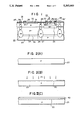
- FIG. 1 is a cross section of an optical semiconductor device according to this invention.
- FIGS. 2(A)-2(E), 3(A)-3(C), 4(A)-4(D), 5(A)-5(C), 6(A)-6(D), 7(A)-7(D) and 8 are cross sections to which reference will be made in describing the process for producing the optical semiconductor device of FIG. 1.
- FIG. 9 is a cross section of an optical semiconductor device according to the prior art.
- a photo diode 21 and an NPN transistor 22 are integrated into a single device.
- a P-type single crystal silicon semiconductor substrate 23 includes an ion-implanted counterdoped region 30 that is doped with phosphorus.
- An intrinsic first epitaxial layer 24 is epitaxially grown by vapor deposition on substrate 23 to a thickness of 5-20 microns.
- a second epitaxial layer 25 is grown by vapor deposition on first epitaxial layer 24 to a thickness of 4 to 6 microns. Second epitaxial layer 25 is doped with phosphorus during growth.
- Substrate 23 has a lower concentration of impurities than is normally provided in an ordinary bipolar IC, resulting in a resistivity of 40 to 60 ohm.cm.
- first epitaxial layer 24 is initially from 1000 to 1500 ohm.cm at the time of growth, but changes to 200 to 1500 ohm.cm. due to diffusion of impurities thereinto during subsequent heat treatment.
- Epitaxial layer 24 forms a central diffusion area.
- Second epitaxial layer 25 is doped to a resistivity of 0.5-3.0 ohm.cm using phosphorus at a concentration of about 10 15 phosphorus atoms per cm 3 .
- First and second epitaxial layers 24 and 25 are electrically isolated by a separating area 26 into a section for photo diode 21 and a section for NPN transistor 22.
- Separating area 26 is formed of a lower separating area 27 diffused above and below the interface between substrate 23 and first epitaxial layer 24, a middle separating area 28 diffused above and below the interface between first epitaxial layer 24 and second epitaxial layer 25, and an upper separating area 29 diffused downward from a surface of second epitaxial layer 25.
- Separating areas 27, 28 and 29 overlap to become joined in forming a single separating area 26 that divides epitaxial layers 24 and 25 into isolated island areas.
- lower separating area 26 is diffused downward into substrate 23 at least to a level below the bottom of counterdoped region 30.
- Approximately from 1 ⁇ 10 11 to 5 ⁇ 10 11 atoms of phosphorous per cm 2 ion-implanted are into the surface of substrate 23 to form a counterdoped region 30.
- N-type phosphorus impurities in counterdoped region 30 offset the P-type impurities of substrate 23 in that region.
- the resistivity of substrate 23 in counterdoped region is increased from 40 to 60 ohm.cm, before counterdoping, to over 200 ohm.cm after counterdoping.
- Thermal treatments diffuse the offset impurities in counterdoped region 30 to a depth of 2 to 10 microns, thereby extending the area of increased resistivity by the same distance into substrate 23.
- N + -type diffusion area 31 which acts as a cathode of photo diode 21, is formed on a portion of the surface of second epitaxial layer 25 of photo diode 21.
- the surface of second epitaxial layer 25 is covered by an oxidized membrane 32 which is etched to produce a plurality of contact holes, through which an aluminum cathode electrode 33 contacts N + -type diffusion area 31.
- An aluminum anode contact 34 extends through a contact hole in oxidized membrane 32 to contact the upper surface of separating area 26 which serves as a low-resistivity anode for photo diode 21.
- An N + -type buried layer 35 spans the interface between first and second epitaxial layers 24, 25 of NPN transistor 22.
- a P-type base area 36 is formed in the surface of transistor 22.
- An N + -type collector contact area 38 of NPN transistor 22 are formed on the surface of transistor 22 outside base area 36.
- An aluminum emitter contact 39 passes through oxidized membrane 32 to contact emitter area 37.
- An aluminum base contact 39' passes through oxidized membrane 32 to contact base area 36.
- An aluminum collector contact 39" passes through oxidized membrane 32 to contact a portion of the surface of second epitaxial area 25 within transistor 22, which serves as the collector of transistor 22.
- the resulting device includes photo diode 21 capable of functioning as an optical signal input unit integrated with NPN transistor 22 which, together with the other circuit elements, can be used as part of a signal processing circuit.
- An IC having the foregoing structure can be produced by the following process:
- a P-type silicon semiconductor substrate 23 with a surface direction of ⁇ 100> is P doped to a resistivity of 40 to 60 ohm.cm is prepared.
- the upper surface of substrate 23 is P counterdoped with phosphorus to a concentration of from 10 11 to 5 ⁇ 10 11 atoms per cm 2 at about 40 KeV, thereby implanting impurities for forming counterdoped region 30.
- the process of ion-implantation for forming counterdoped region 30 is carried out over substantially the entire surface area of substrate 23.
- ion implantation at this stage is masked to occur only in the regions which will ultimately be below the area in which photo diode 21 will be formed.
- substrate is heated in an oxygen atmosphere to develop an insulating oxide layer 40 of from 5000 to 7000 Angstroms thick on the surface of substrate 23.
- oxide layer 40 is coated with a negative photo resist layer 41 by conventional means such as, for example, by spin coating.
- Photo resist layer 41 is baked, exposed and chemically etched by conventional HF etching to produce openings 42 through resist layer 41 and through the underlying oxide layer 40 to expose a corresponding pattern in the upper surface of substrate 23.
- boron is ion implanted at about 80 KeV through openings 42 to a concentration of from 10 14 to 10 15 atoms/cm 2 to form precursors 27' of lower separating areas 27.
- resist layer 41 is removed.
- the device is heat treated at a temperature of about 1150° C. for one hour to partially diffuse precursor 27' into substrate 23.
- oxide layer 40 is removed using a solution of HF in preparation for following steps.
- substrate 23 is placed in an epitaxial growing device (not shown) and heated by a lamp at a temperature of approximately 1,140 C.
- SiH 2 Cl 2 gas and H2 gas are introduced into a reaction tube, thus growing an epitaxial layer 24 of intrinsic material to a thickness of 15 to 20 microns.
- a small amount of autodoping of first epitaxial layer 24 takes place during growth by diffusion of boron P-type impurities from substrate 23 to yield a final epitaxial layer 24 having a relatively high resistivity of 200 to 1500 ohm.cm. Heat treatment during subsequent processing steps will cause further diffusion of impurities from substrate 23 into first epitaxial layer 24.
- a P-type area would be formed between substrate 23 and first epitaxial layer 24 with sufficient concentration to inhibit diffusion within the depletion layer.
- the present invention avoids this difficulty by employing a substrate 23 with a relatively high resistivity of 40 to 60 ohm.cm. Diffusion is minimized, thus preventing the formation of a P + region which might interfere with circuit operation.
- the apparatus is heated in an oxygen-containing atmosphere to produce an insulating oxide layer 45 of from 5000 to 7000 Angstroms thick on the surface of first epitaxial layer 24.
- a resist layer 46 is coated over oxide layer 45, baked, exposed and eched to produce an opening 47 through itself and through oxide layer 45 to expose a portion of the surface of first epitaxial layer 24.
- Resist layer 46 is removed and an antimony layer 48, shown in dashed line, is coated over the device, and especially in opening 47.
- the device is heat treated to diffuse a portion of the antimony into the surface of first epitaxial layer 24 to produce a precursor 35' of N + -type buried layer 35.
- antimony layer 48 is removed and the device is heat treated at 1200° C. for 30 minutes to redevelop oxide layer 45 over opening 47. This heat treatment also diffuses buried layer 35 downward into first epitaxial layer 24.
- a further resist layer 49 is coated over oxide layer 45, dried, exposed and etched with an HF solution to produce three openings 50 through itself and through oxide layer 45, thereby exposing three portions of the surface of first epitaxial layer 24.
- boron is ion implanted at 80 KeV through openings 50 at a concentration of 10 14 to 10 15 atoms.cm 2 to form a precursor 28' of middle separating area 28 of separating area 26.
- resist layer 49 is removed, and the device is heat treated at a temperature of 1150° C. for from 4 to 5 hours to diffuse middle separating area 28 from 6 to 8 microns downward and to diffuse lower separating area 27 from 8 to 10 upward until they overlap to become a single entity.
- oxide layer 45 is removed, and second epitaxial layer 25 is epitaxially grown to a thickness of 4 to 6 microns thick atop the surface of first epitaxial layer 24.
- Second epitaxial layer 24 is N doped using phosphorus in the gas from which it is grown.
- the device is heated in an oxygen containing atmosphere to produce a further oxide layer 51, from 5000 to 7000 Angstroms thick, on the surface of second epitaxial layer 25.
- a resist layer 52 is coated on oxide layer 51, baked, exposed and etched to produce openings 53 congruent with lower and middle separating areas 28 revealing the surface of second epitaxial area 25. Boron is ion implanted through openings 53 to produce precursors 29' for upper separating areas 29.
- the resist layer 52 is removed and the assembly is heat treated at about 1000° C. for 1 to 2 hours to diffuse the boron forming upper separating areas 29 about 1 to 3 microns downward, and to diffuse middle separating areas 28 about 4 to 5 microns so that these two separating areas overlap and join with lower separating areas 27 to form unified separating areas from a distance below the surface of substrate 23 to the upper surface of second epitaxial layer 25.
- the oxide layer 51 is removed to produce the intermediate product shown. It should be noted that lower separating area 27 extends below counterdoped region 30, whereby first and second isolated islands 54 and 55 are isolated by separating areas 26 extending the entire distance from the top surface second epitaxial layer 25 to below the bottom of counterdoped region 30.
- an oxide layer 56 is formed on the surface of second epitaxial layer 25 and is coated with a resist layer 57. Resist layer 57 is baked, exposed and etched to form an opening 58 therethrough and through oxide layer 56 to reveal a portion of the surface of second epitaxial layer 25. Boron is ion implanted at 40 KeV through opening 58 to a concentration of 10 14 to 10 16 atoms/cm 2 to form a precursor 36' of base area 36.
- resist layer 57 is removed and the device is heat treated at about 1100° C. from 1-2 hours to diffuse downward the boron in precursor 36', thereby forming base area 36. During this heat treatment, a further oxide layer 59 is developed on the surface of second epitaxial layer 25.
- a resist layer (not shown) is deposited, and etched to form openings 60 in oxide layer 59.
- a phosphorus layer (not shown) is coated over oxide layer 59 and the device is baked to diffuse some of the phosphorus into portions of the surface of second epitaxial layer 25 corresponding to openings 60. The phosphorus layer is removed and the assembly is baked to diffuse diffusion area 31, emitter area 37 and collector contact area 38 downward.
- oxide layer 59 is removed, and is replaced with oxidized membrane 32 to accommodate electrodes 33, 39, 39' and 39" contacting elements below them.
- Electrodes 33, 39, 39' and 39", as well as interconnection wiring (not shown), are preferably formed by evaporation coating of aluminum-silicon alloy, about 1 to 2 microns thick, atop oxide membrane 32, and etching away unwanted portions.
- etching and boron implantation for these elements may be performed during the formation of base area 36. That is, the portion of the process shown in FIG. 7(B) may be changed to include the formation of openings for the implantation of boron to form upper separating areas 29, at the same time that the opening 58 is formed for the implantation of boron to form base area 36.
- first epitaxial layer 24 is epitaxially grown from intrinsic material, and is only lightly autodoped during growth and subsequent fabrication steps, first epitaxial layer 24 has a high resistivity. This high resistivity places the depletion region mainly within first epitaxial layer 24.
- the depth of the depletion region equals the sum of the diffusion in second epitaxial layer 25 from the foregoing boundary, the diffusion in first epitaxial layer 24, and the diffusion extending to the depth of counterdoped region 30 of substrate 23, a total of 25 to 35 microns.
- the junction capacitance of photo diode 21 decreases with an increase in the depth of the depletion region. As a result, this invention is able to produce high speed responses.
- the impurities (boron) in substrate 23 forms a P-type region in first epitaxial layer 24 by autodoping during epitaxial growth and during subsequent thermal treatment. Since first epitaxial layer is intrinsic, however, the concentration of impurities in this P-type region remains low. This effect is accentuated by the relatively low concentration of impurities (40 to 60 ohm.cm) within substrate 23.
- offset impurities implanted to form counterdoped region 30 in addition to diffusing downward into substrate 23, also diffuse upward into first epitaxial layer 24. They offset the impurities that diffuse into first epitaxial layer 24 and thus offset some of the impurities entering first epitaxial layer due to autodoping. Accordingly, the threshold concentration of impurities necessary to interfere with diffusion within the depletion region is never reached.
- first epitaxial layer 24 When first epitaxial layer 24 is grown, the boron which enters it from substrate 23 or first separating area 27 may unite with silicon atoms or be deposited, thereby changing first epitaxial layer 24 into a P-type region near substrate 23.
- second epitaxial layer 25 is N-type, a PIN junction or a PN junction, suitable for the formation of a deep depletion layer, is easily formed.
- the overall depth of the depletion region of photo diode 21 is thicker than first epitaxial layer 24. As a result, the absorption efficiency of the depletion region for incident light is high. A corresponding decrease in the ratio of carriers occurring in the depth of photo diode 21 increases the operating speed.
- the carriers produced by incident light travel to anode electrode 34 through separating area 26, which has a of low resistivity.
- This low contact resistivity provides low series resistance for photo diode 21.
- the low resistivity of N + -type diffusion area 31 provides direct removal of charges, thereby even further reducing the series resistance.
- the growth of intrinsic first epitaxial layer 24 provides a relatively thick depletion region in first epitaxial layer 24.
- the offset impurities in counterdoped region 30 allow the depletion region to expand into substrate 23. This produces a low junction capacitance and increases the light absorption ratio. This, in turn, prevents liberation of carriers outside depletion region.
- this invention provides a very high speed response photo diode 21.
- First epitaxial layer 24 is grown from intrinsic materials, being lightly doped by autodoping during growth and subsequent processing. It is unnecessary to control the concentration of impurities during growth and simple to obtain high resistivity in this layer. Since only intrinsic material is used to grow epitaxial layer, the vessel in which the epitaxial layer is grown does not become contaminated by a large quantity of boron, as is the case with the prior-art process. Since the vessel is not contaminated with large quantities of boron during epitaxial growth of first epitaxial layer 24, it is not necessary to physically remove the apparatus from the vessel in order to begin the growth of N-type epitaxial layer 25. This reduces maintenance on the device.
- separating area 26 is formed by lower separating area 27, which diffuses upward to join middle separating area 28, which grows downward, the amount by which middle separating area 28 must be diffused is reduced, compared to the prior art. Accordingly, middle separating area 28 can be shallower, and thereby with less horizontal diffusion than is the case with corresponding elements in the prior art. Thus, less horizontal space is taken by middle separating area, and the total real estate occupied by NPN transistor 22 can be relatively small.
Abstract
Description
Claims (18)
Applications Claiming Priority (2)
| Application Number | Priority Date | Filing Date | Title |
|---|---|---|---|
| JP3032929A JP2557750B2 (en) | 1991-02-27 | 1991-02-27 | Optical semiconductor device |
| JP3-032929 | 1991-02-27 |
Publications (1)
| Publication Number | Publication Date |
|---|---|
| US5283460A true US5283460A (en) | 1994-02-01 |
Family
ID=12372610
Family Applications (1)
| Application Number | Title | Priority Date | Filing Date |
|---|---|---|---|
| US07/834,611 Expired - Lifetime US5283460A (en) | 1991-02-27 | 1992-02-12 | Optical semiconductor device |
Country Status (5)
| Country | Link |
|---|---|
| US (1) | US5283460A (en) |
| EP (1) | EP0501316B1 (en) |
| JP (1) | JP2557750B2 (en) |
| KR (1) | KR0182270B1 (en) |
| DE (1) | DE69223664T2 (en) |
Cited By (24)
| Publication number | Priority date | Publication date | Assignee | Title |
|---|---|---|---|---|
| US5382824A (en) * | 1992-07-16 | 1995-01-17 | Landis & Gyr Business Support Ag | Integrated circuit with an integrated color-selective photo diode and an amplifier following the photo-diode |
| US5602415A (en) * | 1994-07-14 | 1997-02-11 | Sharp Kabushiki Kaisha | Light receiving device with isolation regions |
| US5889315A (en) * | 1994-08-18 | 1999-03-30 | National Semiconductor Corporation | Semiconductor structure having two levels of buried regions |
| US6005278A (en) * | 1997-01-27 | 1999-12-21 | Sharp Kabushiki Kaisha | Divided photodiode |
| US6146957A (en) * | 1997-04-01 | 2000-11-14 | Sony Corporation | Method of manufacturing a semiconductor device having a buried region with higher impurity concentration |
| US6184100B1 (en) * | 1995-12-06 | 2001-02-06 | Sony Corporation | Method of manufacturing a photodiode |
| US6249033B1 (en) * | 1997-02-27 | 2001-06-19 | Istituto Nazionale Di Fisica Nucleare | Controlled-drift apparatus for detecting energy and point of incidence of electromagnetic radiations or ionizing particles |
| US6313484B1 (en) * | 1998-12-28 | 2001-11-06 | Sharp Kabushiki Kaisha | Circuit-integrated light-receiving device |
| US6380603B1 (en) * | 1999-11-08 | 2002-04-30 | Sharp Kabushiki Kaisha | Photosensitive device with internal circuitry that includes on the same substrate |
| US6433374B1 (en) * | 2000-10-31 | 2002-08-13 | Sharp Kabushiki Kaisha | Light receiving device with built-in circuit |
| US6469365B1 (en) * | 1998-02-12 | 2002-10-22 | Infineon Technologies Ag | Semiconductor component with a structure for avoiding parallel-path currents and method for fabricating a semiconductor component |
| US20040021194A1 (en) * | 2001-08-22 | 2004-02-05 | Mann Richard A. | Semiconductor device for isolating a photodiode to reduce junction leakage and method of formation |
| US20040046194A1 (en) * | 1999-02-25 | 2004-03-11 | Canon Kabushiki Kaisha | Light-receiving element and photoelectric conversion device |
| US20070114627A1 (en) * | 2005-11-22 | 2007-05-24 | Stmicroelectronics S.A. | Photodetector with an improved resolution |
| US20070145442A1 (en) * | 2005-12-28 | 2007-06-28 | Su Lim | Cmos image sensor |
| US20080012088A1 (en) * | 2006-07-13 | 2008-01-17 | Tetsuya Yamaguchi | Solid-state imaging device and method of manufacturing the same |
| US20090261441A1 (en) * | 2008-04-21 | 2009-10-22 | Hisatada Yasukawa | Optical semiconductor device |
| US7872343B1 (en) | 2007-08-07 | 2011-01-18 | Amkor Technology, Inc. | Dual laminate package structure with embedded elements |
| US20140061844A1 (en) * | 2011-06-09 | 2014-03-06 | Panasonic Corporation | Optical device |
| US8674485B1 (en) | 2010-12-08 | 2014-03-18 | Amkor Technology, Inc. | Semiconductor device including leadframe with downsets |
| CN104051416A (en) * | 2013-03-15 | 2014-09-17 | 半导体元件工业有限责任公司 | Electronic device including vertical conductive regions and a process of forming the same |
| US20140264574A1 (en) * | 2013-03-15 | 2014-09-18 | Semiconductor Components Industries, Llc | Electronic device including vertical conductive regions and a process of forming the same |
| US20170062500A1 (en) * | 2015-08-27 | 2017-03-02 | Renesas Electronics Corporation | Method for manufacturing semiconductor device and semiconductor device |
| US20190280145A1 (en) * | 2016-11-09 | 2019-09-12 | Sharp Kabushiki Kaisha | Avalanche photodiode |
Families Citing this family (9)
| Publication number | Priority date | Publication date | Assignee | Title |
|---|---|---|---|---|
| JP2793085B2 (en) * | 1992-06-25 | 1998-09-03 | 三洋電機株式会社 | Optical semiconductor device and its manufacturing method |
| US6080644A (en) * | 1998-02-06 | 2000-06-27 | Burr-Brown Corporation | Complementary bipolar/CMOS epitaxial structure and process |
| DE19933162B4 (en) * | 1999-07-20 | 2004-11-11 | Institut für Mikroelektronik Stuttgart Stiftung des öffentlichen Rechts | Image cell, image sensor and manufacturing process therefor |
| JP4131059B2 (en) * | 1999-08-23 | 2008-08-13 | ソニー株式会社 | Semiconductor device having light receiving element, optical pickup device, and method of manufacturing semiconductor device having light receiving element |
| JP4919370B2 (en) * | 2005-03-31 | 2012-04-18 | ルネサスエレクトロニクス株式会社 | Semiconductor light receiving device and manufacturing method of semiconductor light receiving device |
| JP4718875B2 (en) * | 2005-03-31 | 2011-07-06 | 株式会社東芝 | Solid-state image sensor |
| US7800146B2 (en) * | 2005-08-26 | 2010-09-21 | Aptina Imaging Corporation | Implanted isolation region for imager pixels |
| JP4709012B2 (en) * | 2006-01-05 | 2011-06-22 | ルネサスエレクトロニクス株式会社 | Optical semiconductor device and manufacturing method thereof |
| US20070241377A1 (en) * | 2006-04-12 | 2007-10-18 | Semicoa | Back-illuminated photo-transistor arrays for computed tomography and other imaging applications |
Citations (1)
| Publication number | Priority date | Publication date | Assignee | Title |
|---|---|---|---|---|
| JPH01205564A (en) * | 1988-02-12 | 1989-08-17 | Hamamatsu Photonics Kk | Optical semiconductor device and its manufacture |
Family Cites Families (3)
| Publication number | Priority date | Publication date | Assignee | Title |
|---|---|---|---|---|
| JPS61154063A (en) * | 1984-12-26 | 1986-07-12 | Toshiba Corp | Optical semiconductor device and manufacture thereof |
| JPH0654957B2 (en) * | 1985-11-13 | 1994-07-20 | キヤノン株式会社 | Photoelectric conversion device |
| US4879470A (en) * | 1987-01-16 | 1989-11-07 | Canon Kabushiki Kaisha | Photoelectric converting apparatus having carrier eliminating means |
-
1991
- 1991-02-27 JP JP3032929A patent/JP2557750B2/en not_active Expired - Lifetime
-
1992
- 1992-02-12 US US07/834,611 patent/US5283460A/en not_active Expired - Lifetime
- 1992-02-20 DE DE69223664T patent/DE69223664T2/en not_active Expired - Fee Related
- 1992-02-20 EP EP92102886A patent/EP0501316B1/en not_active Expired - Lifetime
- 1992-02-25 KR KR1019920002861A patent/KR0182270B1/en not_active IP Right Cessation
Patent Citations (1)
| Publication number | Priority date | Publication date | Assignee | Title |
|---|---|---|---|---|
| JPH01205564A (en) * | 1988-02-12 | 1989-08-17 | Hamamatsu Photonics Kk | Optical semiconductor device and its manufacture |
Cited By (36)
| Publication number | Priority date | Publication date | Assignee | Title |
|---|---|---|---|---|
| US5382824A (en) * | 1992-07-16 | 1995-01-17 | Landis & Gyr Business Support Ag | Integrated circuit with an integrated color-selective photo diode and an amplifier following the photo-diode |
| US5602415A (en) * | 1994-07-14 | 1997-02-11 | Sharp Kabushiki Kaisha | Light receiving device with isolation regions |
| US5889315A (en) * | 1994-08-18 | 1999-03-30 | National Semiconductor Corporation | Semiconductor structure having two levels of buried regions |
| US5899714A (en) * | 1994-08-18 | 1999-05-04 | National Semiconductor Corporation | Fabrication of semiconductor structure having two levels of buried regions |
| US6184100B1 (en) * | 1995-12-06 | 2001-02-06 | Sony Corporation | Method of manufacturing a photodiode |
| US6005278A (en) * | 1997-01-27 | 1999-12-21 | Sharp Kabushiki Kaisha | Divided photodiode |
| US6249033B1 (en) * | 1997-02-27 | 2001-06-19 | Istituto Nazionale Di Fisica Nucleare | Controlled-drift apparatus for detecting energy and point of incidence of electromagnetic radiations or ionizing particles |
| US6146957A (en) * | 1997-04-01 | 2000-11-14 | Sony Corporation | Method of manufacturing a semiconductor device having a buried region with higher impurity concentration |
| US6469365B1 (en) * | 1998-02-12 | 2002-10-22 | Infineon Technologies Ag | Semiconductor component with a structure for avoiding parallel-path currents and method for fabricating a semiconductor component |
| US6313484B1 (en) * | 1998-12-28 | 2001-11-06 | Sharp Kabushiki Kaisha | Circuit-integrated light-receiving device |
| US20040046194A1 (en) * | 1999-02-25 | 2004-03-11 | Canon Kabushiki Kaisha | Light-receiving element and photoelectric conversion device |
| US7235831B2 (en) * | 1999-02-25 | 2007-06-26 | Canon Kabushiki Kaisha | Light-receiving element and photoelectric conversion device |
| US6380603B1 (en) * | 1999-11-08 | 2002-04-30 | Sharp Kabushiki Kaisha | Photosensitive device with internal circuitry that includes on the same substrate |
| US6433374B1 (en) * | 2000-10-31 | 2002-08-13 | Sharp Kabushiki Kaisha | Light receiving device with built-in circuit |
| US7112466B2 (en) * | 2001-08-22 | 2006-09-26 | Ess Technology, Inc. | Semiconductor device for isolating a photodiode to reduce junction leakage and method of formation |
| US20040021194A1 (en) * | 2001-08-22 | 2004-02-05 | Mann Richard A. | Semiconductor device for isolating a photodiode to reduce junction leakage and method of formation |
| US20070114627A1 (en) * | 2005-11-22 | 2007-05-24 | Stmicroelectronics S.A. | Photodetector with an improved resolution |
| US7964928B2 (en) * | 2005-11-22 | 2011-06-21 | Stmicroelectronics S.A. | Photodetector with an improved resolution |
| US20070145442A1 (en) * | 2005-12-28 | 2007-06-28 | Su Lim | Cmos image sensor |
| US7633104B2 (en) * | 2005-12-28 | 2009-12-15 | Dongbu Hitek Co., Ltd. | CMOS image sensor |
| US20080012088A1 (en) * | 2006-07-13 | 2008-01-17 | Tetsuya Yamaguchi | Solid-state imaging device and method of manufacturing the same |
| US7855406B2 (en) * | 2006-07-13 | 2010-12-21 | Kabushiki Kaisha Toshiba | Solid-state imaging device and method of manufacturing the same |
| US7872343B1 (en) | 2007-08-07 | 2011-01-18 | Amkor Technology, Inc. | Dual laminate package structure with embedded elements |
| US8283767B1 (en) | 2007-08-07 | 2012-10-09 | Amkor Technology, Inc. | Dual laminate package structure with embedded elements |
| US20090261441A1 (en) * | 2008-04-21 | 2009-10-22 | Hisatada Yasukawa | Optical semiconductor device |
| US8674485B1 (en) | 2010-12-08 | 2014-03-18 | Amkor Technology, Inc. | Semiconductor device including leadframe with downsets |
| US9136409B2 (en) * | 2011-06-09 | 2015-09-15 | Panasonic Intellectual Property Management Co., Ltd. | Optical device |
| US20140061844A1 (en) * | 2011-06-09 | 2014-03-06 | Panasonic Corporation | Optical device |
| CN104051416A (en) * | 2013-03-15 | 2014-09-17 | 半导体元件工业有限责任公司 | Electronic device including vertical conductive regions and a process of forming the same |
| US20140264574A1 (en) * | 2013-03-15 | 2014-09-18 | Semiconductor Components Industries, Llc | Electronic device including vertical conductive regions and a process of forming the same |
| US9466698B2 (en) * | 2013-03-15 | 2016-10-11 | Semiconductor Components Industries, Llc | Electronic device including vertical conductive regions and a process of forming the same |
| CN104051416B (en) * | 2013-03-15 | 2018-04-13 | 半导体元件工业有限责任公司 | Electronic equipment and its formation process including vertical conduction region |
| US20170062500A1 (en) * | 2015-08-27 | 2017-03-02 | Renesas Electronics Corporation | Method for manufacturing semiconductor device and semiconductor device |
| US9842869B2 (en) * | 2015-08-27 | 2017-12-12 | Renesas Electronics Corporation | Method for manufacturing semiconductor device and semiconductor device |
| US20190280145A1 (en) * | 2016-11-09 | 2019-09-12 | Sharp Kabushiki Kaisha | Avalanche photodiode |
| US10707369B2 (en) * | 2016-11-09 | 2020-07-07 | Sharp Kabushiki Kaisha | Avalanche photodiode |
Also Published As
| Publication number | Publication date |
|---|---|
| JPH04271171A (en) | 1992-09-28 |
| KR0182270B1 (en) | 1999-03-20 |
| EP0501316A2 (en) | 1992-09-02 |
| KR920017263A (en) | 1992-09-26 |
| DE69223664T2 (en) | 1998-07-23 |
| EP0501316A3 (en) | 1994-11-09 |
| JP2557750B2 (en) | 1996-11-27 |
| EP0501316B1 (en) | 1997-12-29 |
| DE69223664D1 (en) | 1998-02-05 |
Similar Documents
| Publication | Publication Date | Title |
|---|---|---|
| US5283460A (en) | Optical semiconductor device | |
| US5418396A (en) | Optical semiconductor device and fabrication method therefor | |
| US4851362A (en) | Method for manufacturing a semiconductor device | |
| US5252851A (en) | Semiconductor integrated circuit with photo diode | |
| US4283837A (en) | Semiconductor device and method of manufacturing same | |
| US5677209A (en) | Method for fabricating a vertical bipolar transistor | |
| EP0076106B1 (en) | Method for producing a bipolar transistor | |
| GB2156583A (en) | Process for producing semiconductor device | |
| EP0051534B1 (en) | A method of fabricating a self-aligned integrated circuit structure using differential oxide growth | |
| US4372030A (en) | Method for producing a semiconductor device | |
| US4132573A (en) | Method of manufacturing a monolithic integrated circuit utilizing epitaxial deposition and simultaneous outdiffusion | |
| US5837553A (en) | Method of making high voltage, junction isolation semiconductor device having dual conductivity type buried regions | |
| US5880002A (en) | Method for making isolated vertical PNP transistor in a digital BiCMOS process | |
| JPH04271172A (en) | Optical semiconductor device | |
| GB2137019A (en) | Semiconductor Device and Method for Manufacturing | |
| US20050179060A1 (en) | Semiconductor device for integrated injection logic cell and process for fabricating the same | |
| KR100208645B1 (en) | Optical semiconductor device | |
| US4469535A (en) | Method of fabricating semiconductor integrated circuit devices | |
| JP2940818B2 (en) | Optical semiconductor device and its manufacturing method | |
| JPH04299860A (en) | Optical semiconductor device | |
| JPH0436578B2 (en) | ||
| EP0296771A2 (en) | Semiconductor device with a buried layer, and method of manufacture | |
| JPH05218055A (en) | Semiconductor device | |
| JPH04245475A (en) | Manufacture of photosemiconductor device | |
| KR19990002164A (en) | Bipolar transistor and method of manufacturing the same |
Legal Events
| Date | Code | Title | Description |
|---|---|---|---|
| AS | Assignment |
Owner name: SANYO ELECTRIC CO., LTD. A CORPORATION OF JAPAN, Free format text: ASSIGNMENT OF ASSIGNORS INTEREST.;ASSIGNOR:MITA, KEIZI;REEL/FRAME:006020/0370 Effective date: 19920206 |
|
| REMI | Maintenance fee reminder mailed | ||
| FEPP | Fee payment procedure |
Free format text: PETITION RELATED TO MAINTENANCE FEES GRANTED (ORIGINAL EVENT CODE: PMFG); ENTITY STATUS OF PATENT OWNER: LARGE ENTITY |
|
| FEPP | Fee payment procedure |
Free format text: PETITION RELATED TO MAINTENANCE FEES FILED (ORIGINAL EVENT CODE: PMFP); ENTITY STATUS OF PATENT OWNER: LARGE ENTITY |
|
| REIN | Reinstatement after maintenance fee payment confirmed | ||
| FP | Lapsed due to failure to pay maintenance fee |
Effective date: 19980204 |
|
| FPAY | Fee payment |
Year of fee payment: 4 |
|
| SULP | Surcharge for late payment | ||
| STCF | Information on status: patent grant |
Free format text: PATENTED CASE |
|
| PRDP | Patent reinstated due to the acceptance of a late maintenance fee |
Effective date: 19981120 |
|
| FEPP | Fee payment procedure |
Free format text: PAYOR NUMBER ASSIGNED (ORIGINAL EVENT CODE: ASPN); ENTITY STATUS OF PATENT OWNER: LARGE ENTITY |
|
| FPAY | Fee payment |
Year of fee payment: 8 |
|
| FPAY | Fee payment |
Year of fee payment: 12 |
|
| FEPP | Fee payment procedure |
Free format text: PAYER NUMBER DE-ASSIGNED (ORIGINAL EVENT CODE: RMPN); ENTITY STATUS OF PATENT OWNER: LARGE ENTITY Free format text: PAYOR NUMBER ASSIGNED (ORIGINAL EVENT CODE: ASPN); ENTITY STATUS OF PATENT OWNER: LARGE ENTITY |
|
| AS | Assignment |
Owner name: SEMICONDUCTOR COMPONENTS INDUSTRIES, LLC, ARIZONA Free format text: ASSIGNMENT OF ASSIGNORS INTEREST;ASSIGNOR:SANYO ELECTRIC CO., LTD.;REEL/FRAME:026594/0385 Effective date: 20110101 |
|
| AS | Assignment |
Owner name: SEMICONDUCTOR COMPONENTS INDUSTRIES, LLC, ARIZONA Free format text: CORRECTIVE ASSIGNMENT TO CORRECT THE INCORRECT #12/577882 PREVIOUSLY RECORDED ON REEL 026594 FRAME 0385. ASSIGNOR(S) HEREBY CONFIRMS THE ASSIGNMENT;ASSIGNOR:SANYO ELECTRIC CO., LTD;REEL/FRAME:032836/0342 Effective date: 20110101 |