US5276748A - Vertically-coupled arrow modulators or switches on silicon - Google Patents
Vertically-coupled arrow modulators or switches on silicon Download PDFInfo
- Publication number
- US5276748A US5276748A US07/797,520 US79752091A US5276748A US 5276748 A US5276748 A US 5276748A US 79752091 A US79752091 A US 79752091A US 5276748 A US5276748 A US 5276748A
- Authority
- US
- United States
- Prior art keywords
- layer
- interference layer
- substrate
- silicon
- interference
- Prior art date
- Legal status (The legal status is an assumption and is not a legal conclusion. Google has not performed a legal analysis and makes no representation as to the accuracy of the status listed.)
- Expired - Lifetime
Links
Images


Classifications
-
- G—PHYSICS
- G02—OPTICS
- G02F—OPTICAL DEVICES OR ARRANGEMENTS FOR THE CONTROL OF LIGHT BY MODIFICATION OF THE OPTICAL PROPERTIES OF THE MEDIA OF THE ELEMENTS INVOLVED THEREIN; NON-LINEAR OPTICS; FREQUENCY-CHANGING OF LIGHT; OPTICAL LOGIC ELEMENTS; OPTICAL ANALOGUE/DIGITAL CONVERTERS
- G02F1/00—Devices or arrangements for the control of the intensity, colour, phase, polarisation or direction of light arriving from an independent light source, e.g. switching, gating or modulating; Non-linear optics
- G02F1/01—Devices or arrangements for the control of the intensity, colour, phase, polarisation or direction of light arriving from an independent light source, e.g. switching, gating or modulating; Non-linear optics for the control of the intensity, phase, polarisation or colour
- G02F1/011—Devices or arrangements for the control of the intensity, colour, phase, polarisation or direction of light arriving from an independent light source, e.g. switching, gating or modulating; Non-linear optics for the control of the intensity, phase, polarisation or colour in optical waveguides, not otherwise provided for in this subclass
-
- G—PHYSICS
- G02—OPTICS
- G02F—OPTICAL DEVICES OR ARRANGEMENTS FOR THE CONTROL OF LIGHT BY MODIFICATION OF THE OPTICAL PROPERTIES OF THE MEDIA OF THE ELEMENTS INVOLVED THEREIN; NON-LINEAR OPTICS; FREQUENCY-CHANGING OF LIGHT; OPTICAL LOGIC ELEMENTS; OPTICAL ANALOGUE/DIGITAL CONVERTERS
- G02F1/00—Devices or arrangements for the control of the intensity, colour, phase, polarisation or direction of light arriving from an independent light source, e.g. switching, gating or modulating; Non-linear optics
- G02F1/01—Devices or arrangements for the control of the intensity, colour, phase, polarisation or direction of light arriving from an independent light source, e.g. switching, gating or modulating; Non-linear optics for the control of the intensity, phase, polarisation or colour
- G02F1/015—Devices or arrangements for the control of the intensity, colour, phase, polarisation or direction of light arriving from an independent light source, e.g. switching, gating or modulating; Non-linear optics for the control of the intensity, phase, polarisation or colour based on semiconductor elements with at least one potential jump barrier, e.g. PN, PIN junction
- G02F1/025—Devices or arrangements for the control of the intensity, colour, phase, polarisation or direction of light arriving from an independent light source, e.g. switching, gating or modulating; Non-linear optics for the control of the intensity, phase, polarisation or colour based on semiconductor elements with at least one potential jump barrier, e.g. PN, PIN junction in an optical waveguide structure
-
- G—PHYSICS
- G02—OPTICS
- G02F—OPTICAL DEVICES OR ARRANGEMENTS FOR THE CONTROL OF LIGHT BY MODIFICATION OF THE OPTICAL PROPERTIES OF THE MEDIA OF THE ELEMENTS INVOLVED THEREIN; NON-LINEAR OPTICS; FREQUENCY-CHANGING OF LIGHT; OPTICAL LOGIC ELEMENTS; OPTICAL ANALOGUE/DIGITAL CONVERTERS
- G02F1/00—Devices or arrangements for the control of the intensity, colour, phase, polarisation or direction of light arriving from an independent light source, e.g. switching, gating or modulating; Non-linear optics
- G02F1/01—Devices or arrangements for the control of the intensity, colour, phase, polarisation or direction of light arriving from an independent light source, e.g. switching, gating or modulating; Non-linear optics for the control of the intensity, phase, polarisation or colour
- G02F1/015—Devices or arrangements for the control of the intensity, colour, phase, polarisation or direction of light arriving from an independent light source, e.g. switching, gating or modulating; Non-linear optics for the control of the intensity, phase, polarisation or colour based on semiconductor elements with at least one potential jump barrier, e.g. PN, PIN junction
- G02F1/0151—Devices or arrangements for the control of the intensity, colour, phase, polarisation or direction of light arriving from an independent light source, e.g. switching, gating or modulating; Non-linear optics for the control of the intensity, phase, polarisation or colour based on semiconductor elements with at least one potential jump barrier, e.g. PN, PIN junction modulating the refractive index
- G02F1/0152—Devices or arrangements for the control of the intensity, colour, phase, polarisation or direction of light arriving from an independent light source, e.g. switching, gating or modulating; Non-linear optics for the control of the intensity, phase, polarisation or colour based on semiconductor elements with at least one potential jump barrier, e.g. PN, PIN junction modulating the refractive index using free carrier effects, e.g. plasma effect
-
- G—PHYSICS
- G02—OPTICS
- G02F—OPTICAL DEVICES OR ARRANGEMENTS FOR THE CONTROL OF LIGHT BY MODIFICATION OF THE OPTICAL PROPERTIES OF THE MEDIA OF THE ELEMENTS INVOLVED THEREIN; NON-LINEAR OPTICS; FREQUENCY-CHANGING OF LIGHT; OPTICAL LOGIC ELEMENTS; OPTICAL ANALOGUE/DIGITAL CONVERTERS
- G02F2201/00—Constructional arrangements not provided for in groups G02F1/00 - G02F7/00
- G02F2201/06—Constructional arrangements not provided for in groups G02F1/00 - G02F7/00 integrated waveguide
- G02F2201/063—Constructional arrangements not provided for in groups G02F1/00 - G02F7/00 integrated waveguide ridge; rib; strip loaded
-
- G—PHYSICS
- G02—OPTICS
- G02F—OPTICAL DEVICES OR ARRANGEMENTS FOR THE CONTROL OF LIGHT BY MODIFICATION OF THE OPTICAL PROPERTIES OF THE MEDIA OF THE ELEMENTS INVOLVED THEREIN; NON-LINEAR OPTICS; FREQUENCY-CHANGING OF LIGHT; OPTICAL LOGIC ELEMENTS; OPTICAL ANALOGUE/DIGITAL CONVERTERS
- G02F2201/00—Constructional arrangements not provided for in groups G02F1/00 - G02F7/00
- G02F2201/30—Constructional arrangements not provided for in groups G02F1/00 - G02F7/00 grating
- G02F2201/302—Constructional arrangements not provided for in groups G02F1/00 - G02F7/00 grating grating coupler
-
- G—PHYSICS
- G02—OPTICS
- G02F—OPTICAL DEVICES OR ARRANGEMENTS FOR THE CONTROL OF LIGHT BY MODIFICATION OF THE OPTICAL PROPERTIES OF THE MEDIA OF THE ELEMENTS INVOLVED THEREIN; NON-LINEAR OPTICS; FREQUENCY-CHANGING OF LIGHT; OPTICAL LOGIC ELEMENTS; OPTICAL ANALOGUE/DIGITAL CONVERTERS
- G02F2202/00—Materials and properties
- G02F2202/10—Materials and properties semiconductor
- G02F2202/101—Ga×As and alloy
-
- G—PHYSICS
- G02—OPTICS
- G02F—OPTICAL DEVICES OR ARRANGEMENTS FOR THE CONTROL OF LIGHT BY MODIFICATION OF THE OPTICAL PROPERTIES OF THE MEDIA OF THE ELEMENTS INVOLVED THEREIN; NON-LINEAR OPTICS; FREQUENCY-CHANGING OF LIGHT; OPTICAL LOGIC ELEMENTS; OPTICAL ANALOGUE/DIGITAL CONVERTERS
- G02F2202/00—Materials and properties
- G02F2202/10—Materials and properties semiconductor
- G02F2202/105—Materials and properties semiconductor single crystal Si
Definitions
- This invention relates to optical modulators and switches, more particularly to integrated optic waveguide modulators and switches.
- Anti-resonant Reflecting Optical Waveguides have several advantages over other types of waveguides. They can be formed upon silicon, using relatively thin layers compared to other waveguides, for easier compatibility with other electronic integrated circuits. At the same time, they can have a large mode for coupling to optical fibers. Additionally, they are relatively easy to manufacture, as they require no exotic materials.
- These waveguides typically consist of a layer of silicon oxide built upon a silicon substrate. An interference layer of silicon is then placed upon the first layer of silicon oxide, followed by another layer of silicon oxide. All of these materials can be deposited with relative ease.
- the silicon layer sandwiched between the two silicon oxide layers functions as a passive interference cladding layer. The thickness of the interference layer is not critical.
- Active optical modulators are normally difficult to produce in or on silicon. Silicon exhibits no linear electro-optic effect, although changes in absorption or refractive index may be induced by modulating the density of free carriers. All-silicon waveguides tend to have a high propagation loss due to these same free-carrier effects and are difficult to fabricate to have a high modulation efficiency, because of poor modal overlap. All-dielectric waveguides can have low loss, but are typically passive and not useful for modulation. Using an ARROW structure in conjunction with vertical coupling will make it possible to combine the low-loss propagation of dielectric waveguides with the capability of modulating or switching light using free-carrier effects.
- the waveguide is an Anti-Resonant Reflecting Optical Waveguide with one interference layer of a semiconductor material between two layers of dielectric material. Free-carrier effects in the interference layer are controlled by application of a current or field to an active electronic element in the layer to modulate light in the layer.
- FIG. 1A shows a side view of an ARROW waveguide adapted to modulate light using free-carrier effects.
- FIG. 1B shows an end view of an ARROW modulator adapted to control free-carrier effects.
- FIG. 2A shows a path of light flowing through an ARROW modulator.
- FIG. 2B shows a top view of an ARROW modulator with a transistor for controlling free-carrier concentration in a semiconductor interference layer.
- FIG. 2C shows an end view of an ARROW modulator with a transistor for controlling free-carrier concentration in a semiconductor interference layer.
- FIG. 3A shows a side view of another ARROW waveguide adapted to modulate light using free-carrier effects.
- FIG. 3B shows an end view of an alternate embodiment of an ARROW waveguide adapted to modulate light using free-carrier effects.
- FIG. 4 shows a manufacturing process that could be used to form an ARROW waveguide device adapted to modulate light using free-carrier effects.
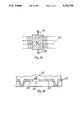
- FIG. 1A A side view of an ARROW modulator that uses the free-carrier effect in semiconductors is shown in FIG. 1A.
- the modulator 10 consists of a substrate 12, which is usually, but not limited to, silicon.
- Substrate 12 has a doped or deposited area 14, which forms the gate of a transistor. The placement of the source and the drain of the transistor will be covered in further discussion.
- the lower cladding of the waveguide 16 This is normally silicon oxide.
- the interference layer 18, which, in this example, is silicon. Other semiconductor materials may also be used.
- the interference layer thickness must be such that constructive interference between the reflections from the top and bottom surfaces of this layer occurs to provide high reflectivity for the mode guided in the core layer.
- Periodic gratings 22 and 24 have been formed into the top of the interference layer 18. This can be accomplished by many ways, including etching. Although shown as two separate gratings, they could also be the two ends of a long section of grating. These gratings allow vertical coupling between the core and the interference layer.
- the core layer, 20, is deposited upon the interference layer, and is typically made out of a dielectric material with high optical transparency, such as silicon oxide, or silicon nitride.
- the lower cladding layer is chosen to be approximately one-half the thickness of the core, to prevent waveguiding in this layer.
- FIG. 1B shows an end view of one embodiment of the modulator 10.
- Substrate 12 has, in addition to gate 14, source contact 26 and drain contact 28.
- the lower cladding 16 is deposited and etched, or just deposited, in such a manner as to allow the interference layer 18 to "touch down" and come in contact with the substrate 12, and its source and drain contacts. This contact allows the modulator to be controlled, if desired, by circuitry in the substrate. Alternatively, contact may be made from the top through the core layer.
- the core layer 20 has a waveguide rib 30, or other structure to transversely confine the light, the cladding underneath the edges of the core is not really necessary anyway. This allows for more freedom in the process design to manufacture the modulator.
- FIG. 2A shows the path of light through the modulator.
- the light enters the core layer 20 from the left of the drawing, shown as arrow 32A.
- the light travels over the grating 22 and is coupled by and through the grating into the interference layer 18, as shown by arrow 32B.
- the interference layer has a higher refractive index than the surrounding core and cladding layers, it acts as a conventional dielectric waveguide for light traveling within it.
- control circuitry, or a control element can be used to control the free-carrier concentration, and thereby modulate the light.
- One method for achieving this is to dope the interference layer to form source and drain regions, and to then apply voltage to gate 14.
- the free-carrier concentration between the source and drain regions will drop drastically in the silicon.
- the transistor may conceivably be operated in either the depletion or the enhancement mode. In either case, the changes in free-carrier concentration will result in changes in the refractive index experienced by light guided in the interference layer. For example, an increase in the free-carrier concentration will result in a decrease in the refractive index for light at the 1.3 ⁇ m wavelength.
- the control of the carrier concentration between the source and drain allows for control of the light that will eventually couple out of the interference layer.
- the previously passive layer of silicon has been turned into an active element for modulating light.
- Lateral confinement for light traveling in this layer is desirable for efficient coupling back into the laterally-confined core layer mode.
- This may be provided, for example, by doping the interference layer to change its refractive index.
- germanium could be used for raising the refractive index of a silicon layer.
- the doping forming the control element may also contribute to lateral confinement.
- FIG. 2B A possible placement of the source and drain regions is shown in FIG. 2B, a top view of a modulator.
- the core layer 20 is seen from above, with rib 30 in the middle.
- Gratings 22 and 24 are shown in dashed lines. These gratings are shown etched onto the interface between the core and interference layers. The preferred placement for the gratings is on the surface of the interference layer, but they may be formed in the material either of the interference layer, or of the core layer.
- Source 27 and drain 29 are in the interference layer, and are hatched to show the active area in the silicon between them.
- Gate 14 is under this region, in or on the substrate below the lower cladding layer. It is hatched differently to highlight its location. Light will be modulated or absorbed depending on the state of the transistor, ON or OFF.
- FIG. 2C shows an end view of this structure.
- Source 27 and drain 29 are of the same doping, either n-type or p-type, demonstrated by identical hatching.
- the gate region 14 is typically in the substrate, as in this case, and under the undoped region between the source and drain regions. The gate must be isolated electrically from the source and drain. As discussed previously, the application of voltage to this control element is used to manage the free-carrier concentration. Additionally, contact regions for the source and drain could be placed in the substrate 12, under regions 27 and 29, where these regions contact the substrate 12.
- FIGS. 3A and 3B Another embodiment for control of the free-carrier effects is shown in FIGS. 3A and 3B.
- a top view of such an embodiment is shown in FIG. 3A.
- a p-i-n diode could be used instead of the transistor in the interference layer as shown previously.
- the entire region that comprises the p-i-n diode has been shaded for viewing clarity.
- P-doped region 34 has a lower boundary at the upper edge of the confinement structure 30, as seen on the drawing.
- the i region 36 is undoped, and lies under the confinement structure 30.
- the n-doped region 38 has an upper boundary at the lower edge of confinement structure 30, as seen on the drawing.
- this structure also provides for lateral optical confinement in the intrinsic region of the interference layer.
- the p-i-n diode structure is actually easier to manufacture and allows for better control of the carrier concentration, than the configurations previously discussed.
- FIG. 3B An end view of this structure is shown in FIG. 3B.
- Layer 20 is shown with the confinement structure 30.
- Region 34 the p-doped region, is to the left of the confinement structure, in the interference layer.
- the interference layer is shown making contact with the semiconductor substrate 12. This is only for electrical connection ease, and better integration of the device. There is no optical reason for this, and this should not be considered as such in the design process.
- the p-i-n diode structure controls the free-carrier concentration in the following way.
- the structure is reverse biased, the intrinsic region in the interference layer is depleted of carriers.
- carriers are injected into this region continuously, where they recombine, allowing current to flow.
- FIG. 4 shows a process for manufacture for one embodiment of the invention.
- the first step, 40 is to prepare a silicon, or other semiconductor material, substrate.
- the substrate could be silicon, gallium arsenide, or other semiconductor material, and may or may not contain electronic control circuitry.
- the next step, 42 is to form the lower cladding, usually out of silicon oxide, or silicon nitride. There are many ways in which to form this layer, one of which is to use thermal oxidation, in the case of silicon.
- the cladding and core layers could be aluminum gallium arsenide (Al x Ga 1-x As).
- the interference layer may be gallium arsenide, or aluminum gallium arsenide with a lower aluminum concentration.
- This is a choice for the next step 44, in which the interference layer is formed. Again, there are many ways in which to form this layer, including epitaxy, but the preferred embodiment for the Si--SiO 2 system is normally to use chemical vapor deposition.
- the gratings or grating in the case of using only one long grating, is formed in the interference layer. This can be done many ways, one of which follows. The interference layer is coated with photoresist, and the resist is exposed to make a grating pattern. The interference layer is then etched to form the grating. Another method is to use electron beam patterning.
- Step 46 can come at various times in the process, depending on the control element used.
- the control element is the lateral p-i-n diode that is formed in the interference layer.
- the interference layer must be doped to form the p-type and n-type doped regions.
- control element step 46 would occur at a different point of the process.
- the core layer is best formed using chemical vapor deposition in step 50, selected from many possibilities.
- step 52 If the use of a confinement structure is determined to be beneficial, this can be formed in step 52.
- One possible process is as follows. First, the core layer is coated with photoresist. The photoresist is then exposed to form a pattern that defines the confinement structure, and the core layer is etched using either a wet or dry etch. Step 54 is to form the upper cladding. Depending on the environment the device is to operated in, this step may not actually be necessary. In previous discussion, the upper cladding was assumed to be air. But, if a special need arises, the upper cladding would be placed upon the core layer.
- the above invention turns a previously passive element of an ARROW waveguide into an active source of modulation. This allows for a device with all of the advantages of an ARROW waveguide discussed previously, plus the addition of modulation.
- the resultant device has thin cladding layers with a thick core layer for more efficient coupling to optical fibers.
- the dielectric core has a low loss for propagation over long distances. Additionally, the process for manufacture of such a device is compatible with standard integrated circuit processing, which leads to the additional advantage of being able to be integrated with and controlled by underlying circuitry.
Abstract
An optical modulator is disclosed. The modulator is based upon an ARROW waveguide, consisting of a substrate, a lower cladding, an interference layer, and a core layer. An electronic element is formed in the structure to control the free-carrier concentration in the interference layer. The light is coupled by grating into the interference layer, where the free-carrier concentration is controlled by the element, which in turn controls the modulation of the light in the interference layer before it is coupled back to the core layer.
Description
1. Field of the Invention
This invention relates to optical modulators and switches, more particularly to integrated optic waveguide modulators and switches.
2. Background of the Invention
Anti-resonant Reflecting Optical Waveguides (ARROW) have several advantages over other types of waveguides. They can be formed upon silicon, using relatively thin layers compared to other waveguides, for easier compatibility with other electronic integrated circuits. At the same time, they can have a large mode for coupling to optical fibers. Additionally, they are relatively easy to manufacture, as they require no exotic materials.
These waveguides typically consist of a layer of silicon oxide built upon a silicon substrate. An interference layer of silicon is then placed upon the first layer of silicon oxide, followed by another layer of silicon oxide. All of these materials can be deposited with relative ease. The silicon layer sandwiched between the two silicon oxide layers functions as a passive interference cladding layer. The thickness of the interference layer is not critical.
Vertical coupling has been achieved in such layered structures made of semiconductor materials by the use of periodic gratings in the materials that make up the structure. This technique can be used to couple light between the top core layer and the interference layer.
Active optical modulators are normally difficult to produce in or on silicon. Silicon exhibits no linear electro-optic effect, although changes in absorption or refractive index may be induced by modulating the density of free carriers. All-silicon waveguides tend to have a high propagation loss due to these same free-carrier effects and are difficult to fabricate to have a high modulation efficiency, because of poor modal overlap. All-dielectric waveguides can have low loss, but are typically passive and not useful for modulation. Using an ARROW structure in conjunction with vertical coupling will make it possible to combine the low-loss propagation of dielectric waveguides with the capability of modulating or switching light using free-carrier effects.
Objects and advantages will be obvious, and will in part appear hereinafter and will be accomplished by the present invention which provides an optical waveguide modulator or switch. The waveguide is an Anti-Resonant Reflecting Optical Waveguide with one interference layer of a semiconductor material between two layers of dielectric material. Free-carrier effects in the interference layer are controlled by application of a current or field to an active electronic element in the layer to modulate light in the layer.
For a complete understanding of the invention, and the advantages thereof, reference is now made to the following description in conjunction with the accompanying drawings, in which:
FIG. 1A shows a side view of an ARROW waveguide adapted to modulate light using free-carrier effects.
FIG. 1B shows an end view of an ARROW modulator adapted to control free-carrier effects.
FIG. 2A shows a path of light flowing through an ARROW modulator.
FIG. 2B shows a top view of an ARROW modulator with a transistor for controlling free-carrier concentration in a semiconductor interference layer.
FIG. 2C shows an end view of an ARROW modulator with a transistor for controlling free-carrier concentration in a semiconductor interference layer.
FIG. 3A shows a side view of another ARROW waveguide adapted to modulate light using free-carrier effects.
FIG. 3B shows an end view of an alternate embodiment of an ARROW waveguide adapted to modulate light using free-carrier effects.
FIG. 4 shows a manufacturing process that could be used to form an ARROW waveguide device adapted to modulate light using free-carrier effects.
A side view of an ARROW modulator that uses the free-carrier effect in semiconductors is shown in FIG. 1A. The modulator 10 consists of a substrate 12, which is usually, but not limited to, silicon. Substrate 12 has a doped or deposited area 14, which forms the gate of a transistor. The placement of the source and the drain of the transistor will be covered in further discussion.
Upon the substrate is the lower cladding of the waveguide, 16. This is normally silicon oxide. On top of the lower cladding layer is the interference layer, 18, which, in this example, is silicon. Other semiconductor materials may also be used. The interference layer thickness must be such that constructive interference between the reflections from the top and bottom surfaces of this layer occurs to provide high reflectivity for the mode guided in the core layer.
FIG. 1B shows an end view of one embodiment of the modulator 10. Substrate 12 has, in addition to gate 14, source contact 26 and drain contact 28. The lower cladding 16 is deposited and etched, or just deposited, in such a manner as to allow the interference layer 18 to "touch down" and come in contact with the substrate 12, and its source and drain contacts. This contact allows the modulator to be controlled, if desired, by circuitry in the substrate. Alternatively, contact may be made from the top through the core layer. As the core layer 20, has a waveguide rib 30, or other structure to transversely confine the light, the cladding underneath the edges of the core is not really necessary anyway. This allows for more freedom in the process design to manufacture the modulator.
FIG. 2A shows the path of light through the modulator. The light enters the core layer 20 from the left of the drawing, shown as arrow 32A. The light travels over the grating 22 and is coupled by and through the grating into the interference layer 18, as shown by arrow 32B. Since the interference layer has a higher refractive index than the surrounding core and cladding layers, it acts as a conventional dielectric waveguide for light traveling within it. While the light is in the interference layer, shown by arrow 32C, control circuitry, or a control element, as will be discussed, can be used to control the free-carrier concentration, and thereby modulate the light. One method for achieving this is to dope the interference layer to form source and drain regions, and to then apply voltage to gate 14. Then, if the resulting transistor is turned off, the free-carrier concentration between the source and drain regions will drop drastically in the silicon. The transistor may conceivably be operated in either the depletion or the enhancement mode. In either case, the changes in free-carrier concentration will result in changes in the refractive index experienced by light guided in the interference layer. For example, an increase in the free-carrier concentration will result in a decrease in the refractive index for light at the 1.3 μm wavelength.
The control of the carrier concentration between the source and drain allows for control of the light that will eventually couple out of the interference layer. The previously passive layer of silicon has been turned into an active element for modulating light.
Lateral confinement for light traveling in this layer is desirable for efficient coupling back into the laterally-confined core layer mode. This may be provided, for example, by doping the interference layer to change its refractive index. For example, germanium could be used for raising the refractive index of a silicon layer. The doping forming the control element may also contribute to lateral confinement.
A possible placement of the source and drain regions is shown in FIG. 2B, a top view of a modulator. The core layer 20 is seen from above, with rib 30 in the middle. Gratings 22 and 24 are shown in dashed lines. These gratings are shown etched onto the interface between the core and interference layers. The preferred placement for the gratings is on the surface of the interference layer, but they may be formed in the material either of the interference layer, or of the core layer. Source 27 and drain 29 are in the interference layer, and are hatched to show the active area in the silicon between them. Gate 14 is under this region, in or on the substrate below the lower cladding layer. It is hatched differently to highlight its location. Light will be modulated or absorbed depending on the state of the transistor, ON or OFF.
FIG. 2C shows an end view of this structure. Source 27 and drain 29 are of the same doping, either n-type or p-type, demonstrated by identical hatching. The gate region 14 is typically in the substrate, as in this case, and under the undoped region between the source and drain regions. The gate must be isolated electrically from the source and drain. As discussed previously, the application of voltage to this control element is used to manage the free-carrier concentration. Additionally, contact regions for the source and drain could be placed in the substrate 12, under regions 27 and 29, where these regions contact the substrate 12.
Another embodiment for control of the free-carrier effects is shown in FIGS. 3A and 3B. A top view of such an embodiment is shown in FIG. 3A. Instead of the transistor in the interference layer as shown previously, a p-i-n diode could be used. The entire region that comprises the p-i-n diode has been shaded for viewing clarity. P-doped region 34 has a lower boundary at the upper edge of the confinement structure 30, as seen on the drawing. The i region 36 is undoped, and lies under the confinement structure 30. The n-doped region 38 has an upper boundary at the lower edge of confinement structure 30, as seen on the drawing. Note that since p-type and n-type doping both reduce the refractive index, this structure also provides for lateral optical confinement in the intrinsic region of the interference layer. The p-i-n diode structure is actually easier to manufacture and allows for better control of the carrier concentration, than the configurations previously discussed.
An end view of this structure is shown in FIG. 3B. Layer 20 is shown with the confinement structure 30. Region 34, the p-doped region, is to the left of the confinement structure, in the interference layer. The interference layer is shown making contact with the semiconductor substrate 12. This is only for electrical connection ease, and better integration of the device. There is no optical reason for this, and this should not be considered as such in the design process.
The p-i-n diode structure controls the free-carrier concentration in the following way. When the structure is reverse biased, the intrinsic region in the interference layer is depleted of carriers. When the structure is forward biased, carriers are injected into this region continuously, where they recombine, allowing current to flow.
FIG. 4 shows a process for manufacture for one embodiment of the invention. The first step, 40, is to prepare a silicon, or other semiconductor material, substrate. The substrate could be silicon, gallium arsenide, or other semiconductor material, and may or may not contain electronic control circuitry. The next step, 42, is to form the lower cladding, usually out of silicon oxide, or silicon nitride. There are many ways in which to form this layer, one of which is to use thermal oxidation, in the case of silicon.
If the substrate is gallium arsenide, the cladding and core layers could be aluminum gallium arsenide (Alx Ga1-x As). The interference layer may be gallium arsenide, or aluminum gallium arsenide with a lower aluminum concentration. This is a choice for the next step 44, in which the interference layer is formed. Again, there are many ways in which to form this layer, including epitaxy, but the preferred embodiment for the Si--SiO2 system is normally to use chemical vapor deposition. In step 48 the gratings or grating, in the case of using only one long grating, is formed in the interference layer. This can be done many ways, one of which follows. The interference layer is coated with photoresist, and the resist is exposed to make a grating pattern. The interference layer is then etched to form the grating. Another method is to use electron beam patterning.
Obviously, if an embodiment where the control element is formed elsewhere in the structure is used, the control element step 46 would occur at a different point of the process. The core layer is best formed using chemical vapor deposition in step 50, selected from many possibilities.
If the use of a confinement structure is determined to be beneficial, this can be formed in step 52. One possible process is as follows. First, the core layer is coated with photoresist. The photoresist is then exposed to form a pattern that defines the confinement structure, and the core layer is etched using either a wet or dry etch. Step 54 is to form the upper cladding. Depending on the environment the device is to operated in, this step may not actually be necessary. In previous discussion, the upper cladding was assumed to be air. But, if a special need arises, the upper cladding would be placed upon the core layer.
The above invention turns a previously passive element of an ARROW waveguide into an active source of modulation. This allows for a device with all of the advantages of an ARROW waveguide discussed previously, plus the addition of modulation. The resultant device has thin cladding layers with a thick core layer for more efficient coupling to optical fibers. The dielectric core has a low loss for propagation over long distances. Additionally, the process for manufacture of such a device is compatible with standard integrated circuit processing, which leads to the additional advantage of being able to be integrated with and controlled by underlying circuitry.
Thus, although there has been described to this point a particular embodiment for an integrated-optic waveguide modulator, it is not intended that such specific references be considered as limitations upon the scope of this invention except in-so-far as set forth in the following claims.
Claims (12)
1. A method for forming an optical modulator comprising:
a. preparing a semiconductor substrate;
b. building a lower cladding layer of a predetermined thickness upon said substrate;
c. depositing an interference layer upon said lower cladding layer;
d. depositing a core layer upon said interference layer;
e. placing gratings in said modulator operable to couple light between said core layer and said interference layer; and
f. forming an electronic element in said modulator to control free-carrier effects in said interference layer.
2. The method as claimed in claim 1 wherein said building step comprises thermal oxidation.
3. The method as claimed in claim 1 wherein said depositing an interference layer step comprises chemical vapor deposition.
4. The method as claimed in claim 1 wherein said placing step comprises patterning and etching said interference layer.
5. The method as claimed in claim 1 wherein said depositing a core layer step comprises chemical vapor deposition.
6. The method as claimed in claim 1 wherein said forming step comprises doping the interference layer.
7. The method as claimed in claim 6 wherein said forming step further comprises doping the substrate.
8. The method as claimed in claim 6 wherein said forming step further comprises depositing an electrode.
9. The method as claimed in claim 1 wherein said electronic element is a transistor.
10. The method as claimed in claim 1 wherein said electronic element is a diode.
11. The method as claimed in claim 1 wherein said substrate is silicon.
12. The method as claimed in claim 1 wherein said substrate is gallium arsenide.
Priority Applications (7)
| Application Number | Priority Date | Filing Date | Title |
|---|---|---|---|
| US07/797,520 US5276748A (en) | 1991-11-22 | 1991-11-22 | Vertically-coupled arrow modulators or switches on silicon |
| CA002080672A CA2080672C (en) | 1991-11-22 | 1992-10-15 | Vertically-coupled arrow modulators or switches on silicon |
| DE69224272T DE69224272T2 (en) | 1991-11-22 | 1992-11-19 | Modulator or switch with vertically coupled, anti-resonant reflective optical waveguides ("ARROW") on silicon |
| EP92119714A EP0543369B1 (en) | 1991-11-22 | 1992-11-19 | Modulator or switch with vertically-coupled anti-resonant reflecting optical waveguides ("arrow") on silicon |
| JP31232192A JP3396498B2 (en) | 1991-11-22 | 1992-11-20 | Optical modulator and its manufacturing method |
| US08/100,837 US5367582A (en) | 1991-11-22 | 1993-07-30 | Vertically-coupled arrow modulators or switches on silicon |
| US08/335,233 US5502779A (en) | 1991-11-22 | 1994-11-07 | Integrated optical modulator and waveguide and method |
Applications Claiming Priority (1)
| Application Number | Priority Date | Filing Date | Title |
|---|---|---|---|
| US07/797,520 US5276748A (en) | 1991-11-22 | 1991-11-22 | Vertically-coupled arrow modulators or switches on silicon |
Related Child Applications (1)
| Application Number | Title | Priority Date | Filing Date |
|---|---|---|---|
| US08/100,837 Division US5367582A (en) | 1991-11-22 | 1993-07-30 | Vertically-coupled arrow modulators or switches on silicon |
Publications (1)
| Publication Number | Publication Date |
|---|---|
| US5276748A true US5276748A (en) | 1994-01-04 |
Family
ID=25171065
Family Applications (3)
| Application Number | Title | Priority Date | Filing Date |
|---|---|---|---|
| US07/797,520 Expired - Lifetime US5276748A (en) | 1991-11-22 | 1991-11-22 | Vertically-coupled arrow modulators or switches on silicon |
| US08/100,837 Expired - Lifetime US5367582A (en) | 1991-11-22 | 1993-07-30 | Vertically-coupled arrow modulators or switches on silicon |
| US08/335,233 Expired - Lifetime US5502779A (en) | 1991-11-22 | 1994-11-07 | Integrated optical modulator and waveguide and method |
Family Applications After (2)
| Application Number | Title | Priority Date | Filing Date |
|---|---|---|---|
| US08/100,837 Expired - Lifetime US5367582A (en) | 1991-11-22 | 1993-07-30 | Vertically-coupled arrow modulators or switches on silicon |
| US08/335,233 Expired - Lifetime US5502779A (en) | 1991-11-22 | 1994-11-07 | Integrated optical modulator and waveguide and method |
Country Status (5)
| Country | Link |
|---|---|
| US (3) | US5276748A (en) |
| EP (1) | EP0543369B1 (en) |
| JP (1) | JP3396498B2 (en) |
| CA (1) | CA2080672C (en) |
| DE (1) | DE69224272T2 (en) |
Cited By (8)
| Publication number | Priority date | Publication date | Assignee | Title |
|---|---|---|---|---|
| US5367582A (en) * | 1991-11-22 | 1994-11-22 | Texas Instruments Incorporated | Vertically-coupled arrow modulators or switches on silicon |
| US5568574A (en) * | 1995-06-12 | 1996-10-22 | University Of Southern California | Modulator-based photonic chip-to-chip interconnections for dense three-dimensional multichip module integration |
| US5692076A (en) * | 1995-12-13 | 1997-11-25 | Universite Laval | Antiresonant waveguide apparatus for periodically selecting a series of at least one optical wavelength from an incoming light signal |
| KR100418262B1 (en) * | 2002-05-14 | 2004-02-14 | 한국전자통신연구원 | Multimode interference coupler, multi-layer optical planar waveguide using the same and method of manufacturing the same |
| US20040258358A1 (en) * | 2001-11-15 | 2004-12-23 | Duguay Michel A | Segmented waveguide array grating filters |
| US6993224B1 (en) | 2001-11-15 | 2006-01-31 | UNIVERSITé LAVAL | Segmented waveguide array gratings (SWAG)-based archival optical memory |
| US20090297093A1 (en) * | 2008-05-28 | 2009-12-03 | Lightwire, Inc. | Low index, large mode field diameter optical coupler |
| US20150212385A1 (en) * | 2014-01-30 | 2015-07-30 | Fabio Alessio Marino | Semiconductor Interferometric Device |
Families Citing this family (36)
| Publication number | Priority date | Publication date | Assignee | Title |
|---|---|---|---|---|
| US5577138A (en) * | 1995-08-17 | 1996-11-19 | Lucent Technologies Inc. | Integrated-circuit optical network unit |
| US5577139A (en) * | 1995-08-17 | 1996-11-19 | Lucent Technologies Inc. | Integrated-circuit optical network unit |
| US5903683A (en) * | 1997-09-10 | 1999-05-11 | The United States Of America As Represented By The National Security Agency | Device for modulating an optical signal using a single wave guide |
| US5987196A (en) * | 1997-11-06 | 1999-11-16 | Micron Technology, Inc. | Semiconductor structure having an optical signal path in a substrate and method for forming the same |
| US6330376B1 (en) | 1997-12-19 | 2001-12-11 | Intel Corporation | Higher order rejection method and apparatus for optical modulator |
| US6374003B1 (en) | 1997-12-19 | 2002-04-16 | Intel Corporation | Method and apparatus for optically modulating light through the back side of an integrated circuit die using a plurality of optical beams |
| US6052498A (en) * | 1997-12-19 | 2000-04-18 | Intel Corporation | Method and apparatus providing an optical input/output bus through the back side of an integrated circuit die |
| US6075908A (en) * | 1997-12-19 | 2000-06-13 | Intel Corporation | Method and apparatus for optically modulating light through the back side of an integrated circuit die |
| US6049639A (en) * | 1997-12-19 | 2000-04-11 | Intel Corporation | Method and apparatus providing optical input/output through the back side of an integrated circuit die |
| US6393169B1 (en) | 1997-12-19 | 2002-05-21 | Intel Corporation | Method and apparatus for providing optical interconnection |
| US6587605B2 (en) | 1999-01-06 | 2003-07-01 | Intel Corporation | Method and apparatus for providing optical interconnection |
| US6215577B1 (en) | 1999-10-25 | 2001-04-10 | Intel Corporation | Method and apparatus for optically modulating an optical beam with a multi-pass wave-guided optical modulator |
| US6501092B1 (en) | 1999-10-25 | 2002-12-31 | Intel Corporation | Integrated semiconductor superlattice optical modulator |
| US6268953B1 (en) | 1999-12-02 | 2001-07-31 | Intel Corporation | Method and apparatus for optically modulating an optical beam with long interaction length optical modulator |
| US6351326B1 (en) | 1999-12-14 | 2002-02-26 | Intel Corporation | Method and apparatus for optically modulating light utilizing a resonant cavity structure |
| GB2373343A (en) * | 2001-03-16 | 2002-09-18 | Bookham Technology Plc | Rib waveguide for connection to an optical component |
| US6748125B2 (en) | 2001-05-17 | 2004-06-08 | Sioptical, Inc. | Electronic semiconductor control of light in optical waveguide |
| EP1402298B1 (en) * | 2001-05-17 | 2016-09-21 | Cisco Technology, Inc. | Electronic semiconductor control of light in optical waveguide |
| US6690844B2 (en) | 2001-05-17 | 2004-02-10 | Optronx, Inc. | Optical fiber apparatus and associated method |
| US6526187B1 (en) | 2001-05-17 | 2003-02-25 | Optronx, Inc. | Polarization control apparatus and associated method |
| US6625348B2 (en) | 2001-05-17 | 2003-09-23 | Optron X, Inc. | Programmable delay generator apparatus and associated method |
| US6947615B2 (en) | 2001-05-17 | 2005-09-20 | Sioptical, Inc. | Optical lens apparatus and associated method |
| US6654511B2 (en) | 2001-05-17 | 2003-11-25 | Sioptical, Inc. | Optical modulator apparatus and associated method |
| US6608945B2 (en) | 2001-05-17 | 2003-08-19 | Optronx, Inc. | Self-aligning modulator method and associated apparatus |
| US6493502B1 (en) | 2001-05-17 | 2002-12-10 | Optronx, Inc. | Dynamic gain equalizer method and associated apparatus |
| US6603889B2 (en) | 2001-05-17 | 2003-08-05 | Optronx, Inc. | Optical deflector apparatus and associated method |
| US6646747B2 (en) | 2001-05-17 | 2003-11-11 | Sioptical, Inc. | Interferometer apparatus and associated method |
| US6891685B2 (en) * | 2001-05-17 | 2005-05-10 | Sioptical, Inc. | Anisotropic etching of optical components |
| US6963118B2 (en) * | 2001-05-17 | 2005-11-08 | Sioptical, Inc. | Hybrid active and electronic circuit with evanescent coupling |
| US6912330B2 (en) | 2001-05-17 | 2005-06-28 | Sioptical Inc. | Integrated optical/electronic circuits and associated methods of simultaneous generation thereof |
| US6580864B1 (en) * | 2002-01-14 | 2003-06-17 | Applied Wdm, Inc. | Birefringence free optical waveguide structures |
| US6993236B1 (en) * | 2002-06-24 | 2006-01-31 | Luxtera, Inc. | Polysilicon and silicon dioxide light scatterers for silicon waveguides on five layer substrates |
| US7010208B1 (en) * | 2002-06-24 | 2006-03-07 | Luxtera, Inc. | CMOS process silicon waveguides |
| KR101115735B1 (en) * | 2004-02-26 | 2012-03-06 | 시옵티컬 인코포레이티드 | Active manipulation of light in a silicon-on-insulator SOI structure |
| SE1051151A1 (en) * | 2010-11-03 | 2012-05-04 | Brokk Ab | Breaking hammer on a working machine equipped with maneuverable arm |
| JP2015064413A (en) * | 2013-09-24 | 2015-04-09 | 富士通株式会社 | Optical semiconductor element and manufacturing method therefor |
Citations (3)
| Publication number | Priority date | Publication date | Assignee | Title |
|---|---|---|---|---|
| US4869568A (en) * | 1987-09-29 | 1989-09-26 | Siemens Aktiengesellschaft | Arrangement comprising a planarly extending thin-film waveguide |
| US4904045A (en) * | 1988-03-25 | 1990-02-27 | American Telephone And Telegraph Company | Grating coupler with monolithically integrated quantum well index modulator |
| US4971415A (en) * | 1984-11-16 | 1990-11-20 | Canon Kabushiki Kaisha | Multibeam emitting device |
Family Cites Families (10)
| Publication number | Priority date | Publication date | Assignee | Title |
|---|---|---|---|---|
| US4715672A (en) * | 1986-01-06 | 1987-12-29 | American Telephone And Telegraph Company | Optical waveguide utilizing an antiresonant layered structure |
| US4745607A (en) * | 1986-10-08 | 1988-05-17 | American Telephone And Telegraph Company, At&T Bell Laboratories | Interlayer directional coupling in antiresonant reflecting optical waveguides |
| FR2647965A1 (en) * | 1989-05-30 | 1990-12-07 | Thomson Csf | Electro-optical modulator of the field-effect transistor type |
| DE3931588A1 (en) * | 1989-09-22 | 1991-04-04 | Standard Elektrik Lorenz Ag | INTERFEROMETRIC SEMICONDUCTOR LASER |
| JPH03228032A (en) * | 1990-02-01 | 1991-10-09 | Mitsubishi Electric Corp | Optical directional coupler |
| DE4011860A1 (en) * | 1990-04-09 | 1991-10-10 | Siemens Ag | SEMICONDUCTOR ELEMENT WITH A SILICON LAYER |
| EP0466082B1 (en) * | 1990-07-09 | 1997-05-02 | Canon Kabushiki Kaisha | Method of modulating light and optical modulator |
| US5165105A (en) * | 1991-08-02 | 1992-11-17 | Minnesota Minning And Manufacturing Company | Separate confinement electroabsorption modulator utilizing the Franz-Keldysh effect |
| US5276748A (en) * | 1991-11-22 | 1994-01-04 | Texas Instruments Incorporated | Vertically-coupled arrow modulators or switches on silicon |
| US5253314A (en) * | 1992-01-31 | 1993-10-12 | At&T Bell Laboratories | Tunable optical waveguide coupler |
-
1991
- 1991-11-22 US US07/797,520 patent/US5276748A/en not_active Expired - Lifetime
-
1992
- 1992-10-15 CA CA002080672A patent/CA2080672C/en not_active Expired - Fee Related
- 1992-11-19 DE DE69224272T patent/DE69224272T2/en not_active Expired - Fee Related
- 1992-11-19 EP EP92119714A patent/EP0543369B1/en not_active Expired - Lifetime
- 1992-11-20 JP JP31232192A patent/JP3396498B2/en not_active Expired - Fee Related
-
1993
- 1993-07-30 US US08/100,837 patent/US5367582A/en not_active Expired - Lifetime
-
1994
- 1994-11-07 US US08/335,233 patent/US5502779A/en not_active Expired - Lifetime
Patent Citations (3)
| Publication number | Priority date | Publication date | Assignee | Title |
|---|---|---|---|---|
| US4971415A (en) * | 1984-11-16 | 1990-11-20 | Canon Kabushiki Kaisha | Multibeam emitting device |
| US4869568A (en) * | 1987-09-29 | 1989-09-26 | Siemens Aktiengesellschaft | Arrangement comprising a planarly extending thin-film waveguide |
| US4904045A (en) * | 1988-03-25 | 1990-02-27 | American Telephone And Telegraph Company | Grating coupler with monolithically integrated quantum well index modulator |
Non-Patent Citations (6)
| Title |
|---|
| Duguay, M. A., Kokubun, Y., Koch, T. L., Pfeiffer, L., "Antiresonant Reflecting Optical Waveguides in SiO2 -Si Multilayer Structures", Applied Physics Letters, vol. 49, pp. 13-15, 1986. |
| Duguay, M. A., Kokubun, Y., Koch, T. L., Pfeiffer, L., Antiresonant Reflecting Optical Waveguides in SiO 2 Si Multilayer Structures , Applied Physics Letters, vol. 49, pp. 13 15, 1986. * |
| Koch, T. L., Burkhardt, E. G., Storz, F. G., Bridges, T. J., Sizer, T., II, "Vertically Grating-coupled ARROW Structures for III-V Integrated Optics," IEEE Journal of Quantum Electronics, QE-23, pp. 889-897, 1987. |
| Koch, T. L., Burkhardt, E. G., Storz, F. G., Bridges, T. J., Sizer, T., II, Vertically Grating coupled ARROW Structures for III V Integrated Optics, IEEE Journal of Quantum Electronics, QE 23, pp. 889 897, 1987. * |
| Soref, R. A., Lorenzo, J. P., "All-silicon Active and Passive Guided-wave Components for λ=1.3 and 1.6 μm," IEEE Journal of Quantum Electronics, QE-22, pp. 873-879, 1986. |
| Soref, R. A., Lorenzo, J. P., All silicon Active and Passive Guided wave Components for 1.3 and 1.6 m, IEEE Journal of Quantum Electronics, QE 22, pp. 873 879, 1986. * |
Cited By (12)
| Publication number | Priority date | Publication date | Assignee | Title |
|---|---|---|---|---|
| US5367582A (en) * | 1991-11-22 | 1994-11-22 | Texas Instruments Incorporated | Vertically-coupled arrow modulators or switches on silicon |
| US5502779A (en) * | 1991-11-22 | 1996-03-26 | Texas Instruments Incorporated | Integrated optical modulator and waveguide and method |
| US5568574A (en) * | 1995-06-12 | 1996-10-22 | University Of Southern California | Modulator-based photonic chip-to-chip interconnections for dense three-dimensional multichip module integration |
| US5692076A (en) * | 1995-12-13 | 1997-11-25 | Universite Laval | Antiresonant waveguide apparatus for periodically selecting a series of at least one optical wavelength from an incoming light signal |
| US20040258358A1 (en) * | 2001-11-15 | 2004-12-23 | Duguay Michel A | Segmented waveguide array grating filters |
| US6993224B1 (en) | 2001-11-15 | 2006-01-31 | UNIVERSITé LAVAL | Segmented waveguide array gratings (SWAG)-based archival optical memory |
| US6999662B2 (en) | 2001-11-15 | 2006-02-14 | UNIVERSITé LAVAL | Segmented waveguide array grating filters |
| KR100418262B1 (en) * | 2002-05-14 | 2004-02-14 | 한국전자통신연구원 | Multimode interference coupler, multi-layer optical planar waveguide using the same and method of manufacturing the same |
| US20090297093A1 (en) * | 2008-05-28 | 2009-12-03 | Lightwire, Inc. | Low index, large mode field diameter optical coupler |
| US8031991B2 (en) | 2008-05-28 | 2011-10-04 | Lightwire Inc. | Low index, large mode field diameter optical coupler |
| US20150212385A1 (en) * | 2014-01-30 | 2015-07-30 | Fabio Alessio Marino | Semiconductor Interferometric Device |
| US9726913B2 (en) * | 2014-01-30 | 2017-08-08 | Awenyx Inc. | Semiconductor interferometric device |
Also Published As
| Publication number | Publication date |
|---|---|
| JPH06202052A (en) | 1994-07-22 |
| EP0543369B1 (en) | 1998-01-28 |
| US5367582A (en) | 1994-11-22 |
| US5502779A (en) | 1996-03-26 |
| EP0543369A1 (en) | 1993-05-26 |
| JP3396498B2 (en) | 2003-04-14 |
| CA2080672A1 (en) | 1993-05-23 |
| CA2080672C (en) | 2002-09-24 |
| DE69224272D1 (en) | 1998-03-05 |
| DE69224272T2 (en) | 1998-07-23 |
Similar Documents
| Publication | Publication Date | Title |
|---|---|---|
| US5276748A (en) | Vertically-coupled arrow modulators or switches on silicon | |
| JP2681044B2 (en) | Light modulator | |
| US4840446A (en) | Photo semiconductor device having a multi-quantum well structure | |
| US6633692B2 (en) | High carrier injection optical waveguide switch | |
| US20170299902A1 (en) | Optoelectronic component | |
| US5048907A (en) | Electric field induced quantum well waveguides | |
| JP2873062B2 (en) | Optical integrated device and method of manufacturing the same | |
| US4943133A (en) | Low loss semiconductor optical phase modulator | |
| US4796274A (en) | Semiconductor device with distributed bragg reflector | |
| US4746183A (en) | Electrically controlled integrated optical switch | |
| JPS62174728A (en) | Optical switch | |
| US7865053B2 (en) | Multi-semiconductor slab electro-optic modulator and process for using the same | |
| US4744616A (en) | Monolithic electro-optic modulator array | |
| JP2002503825A (en) | Optical structure and method for manufacturing optical structure | |
| US5581108A (en) | Optical Switching device | |
| JP7276452B2 (en) | optical modulator | |
| WO2023238184A1 (en) | Optical modulator | |
| GB2265252A (en) | An electro-optic device | |
| US6891986B2 (en) | Optical switch | |
| JPH0719001B2 (en) | Semiconductor optical switch | |
| Mikami et al. | InGaAsP/InP optical waveguide switch operated by a carrier-induced change in the refractive index | |
| JPH0583889B2 (en) | ||
| JPS60173519A (en) | Semiconductor optical switch | |
| Sun et al. | Novel large cross-section single-mode AlGaAs/GaAs asymmetric optical switch based on carrier injection effect | |
| Aronson et al. | Integrated‐optical switch arrays in GaAs based on electrically controlled dynamic free carrier gratings |
Legal Events
| Date | Code | Title | Description |
|---|---|---|---|
| AS | Assignment |
Owner name: TEXAS INSTRUMENTS INCORPORATED A CORP. OF DELAWA Free format text: ASSIGNMENT OF ASSIGNORS INTEREST.;ASSIGNOR:MAGEL, GREGORY A.;REEL/FRAME:005928/0946 Effective date: 19911122 |
|
| STCF | Information on status: patent grant |
Free format text: PATENTED CASE |
|
| FPAY | Fee payment |
Year of fee payment: 4 |
|
| FPAY | Fee payment |
Year of fee payment: 8 |
|
| FPAY | Fee payment |
Year of fee payment: 12 |