US5252835A - Machining oxide thin-films with an atomic force microscope: pattern and object formation on the nanometer scale - Google Patents
Machining oxide thin-films with an atomic force microscope: pattern and object formation on the nanometer scale Download PDFInfo
- Publication number
- US5252835A US5252835A US07/916,215 US91621592A US5252835A US 5252835 A US5252835 A US 5252835A US 91621592 A US91621592 A US 91621592A US 5252835 A US5252835 A US 5252835A
- Authority
- US
- United States
- Prior art keywords
- moo
- afm
- mos
- atomic force
- force microscope
- Prior art date
- Legal status (The legal status is an assumption and is not a legal conclusion. Google has not performed a legal analysis and makes no representation as to the accuracy of the status listed.)
- Expired - Fee Related
Links
- 238000003754 machining Methods 0.000 title claims abstract description 7
- 239000010409 thin film Substances 0.000 title claims description 4
- 230000015572 biosynthetic process Effects 0.000 title description 2
- 238000000034 method Methods 0.000 claims description 7
- 238000003384 imaging method Methods 0.000 claims description 5
- JKQOBWVOAYFWKG-UHFFFAOYSA-N molybdenum trioxide Chemical compound O=[Mo](=O)=O JKQOBWVOAYFWKG-UHFFFAOYSA-N 0.000 abstract description 76
- 229910052961 molybdenite Inorganic materials 0.000 abstract description 22
- 229910052982 molybdenum disulfide Inorganic materials 0.000 abstract description 22
- CWQXQMHSOZUFJS-UHFFFAOYSA-N molybdenum disulfide Chemical compound S=[Mo]=S CWQXQMHSOZUFJS-UHFFFAOYSA-N 0.000 abstract description 21
- 239000000758 substrate Substances 0.000 abstract description 8
- 239000002086 nanomaterial Substances 0.000 abstract description 3
- 238000001459 lithography Methods 0.000 abstract 1
- 239000010410 layer Substances 0.000 description 7
- 239000013078 crystal Substances 0.000 description 5
- 239000000463 material Substances 0.000 description 5
- 230000003647 oxidation Effects 0.000 description 5
- 238000007254 oxidation reaction Methods 0.000 description 5
- 238000000089 atomic force micrograph Methods 0.000 description 4
- 239000010408 film Substances 0.000 description 4
- 238000012986 modification Methods 0.000 description 4
- 230000004048 modification Effects 0.000 description 4
- 238000013519 translation Methods 0.000 description 4
- 238000000059 patterning Methods 0.000 description 3
- 230000008569 process Effects 0.000 description 3
- IJGRMHOSHXDMSA-UHFFFAOYSA-N Atomic nitrogen Chemical compound N#N IJGRMHOSHXDMSA-UHFFFAOYSA-N 0.000 description 2
- 229910007277 Si3 N4 Inorganic materials 0.000 description 2
- VYPSYNLAJGMNEJ-UHFFFAOYSA-N Silicium dioxide Chemical compound O=[Si]=O VYPSYNLAJGMNEJ-UHFFFAOYSA-N 0.000 description 2
- 238000002474 experimental method Methods 0.000 description 2
- PCHJSUWPFVWCPO-UHFFFAOYSA-N gold Chemical compound [Au] PCHJSUWPFVWCPO-UHFFFAOYSA-N 0.000 description 2
- 239000010931 gold Substances 0.000 description 2
- 229910052737 gold Inorganic materials 0.000 description 2
- 239000000314 lubricant Substances 0.000 description 2
- 229910044991 metal oxide Inorganic materials 0.000 description 2
- 150000004706 metal oxides Chemical class 0.000 description 2
- 239000012044 organic layer Substances 0.000 description 2
- 229910052814 silicon oxide Inorganic materials 0.000 description 2
- 229910003149 α-MoO3 Inorganic materials 0.000 description 2
- XUIMIQQOPSSXEZ-UHFFFAOYSA-N Silicon Chemical compound [Si] XUIMIQQOPSSXEZ-UHFFFAOYSA-N 0.000 description 1
- 238000001015 X-ray lithography Methods 0.000 description 1
- QVGXLLKOCUKJST-UHFFFAOYSA-N atomic oxygen Chemical compound [O] QVGXLLKOCUKJST-UHFFFAOYSA-N 0.000 description 1
- 230000005540 biological transmission Effects 0.000 description 1
- 238000012512 characterization method Methods 0.000 description 1
- 239000011248 coating agent Substances 0.000 description 1
- 238000000576 coating method Methods 0.000 description 1
- 238000011161 development Methods 0.000 description 1
- 238000009792 diffusion process Methods 0.000 description 1
- 238000010494 dissociation reaction Methods 0.000 description 1
- 230000005593 dissociations Effects 0.000 description 1
- 238000002003 electron diffraction Methods 0.000 description 1
- 238000001493 electron microscopy Methods 0.000 description 1
- 238000005516 engineering process Methods 0.000 description 1
- 230000001788 irregular Effects 0.000 description 1
- 238000000608 laser ablation Methods 0.000 description 1
- 230000007246 mechanism Effects 0.000 description 1
- 238000005459 micromachining Methods 0.000 description 1
- 229910052757 nitrogen Inorganic materials 0.000 description 1
- 230000003287 optical effect Effects 0.000 description 1
- 239000001301 oxygen Substances 0.000 description 1
- 229910052760 oxygen Inorganic materials 0.000 description 1
- 238000004838 photoelectron emission spectroscopy Methods 0.000 description 1
- 238000000746 purification Methods 0.000 description 1
- 230000003252 repetitive effect Effects 0.000 description 1
- 238000012552 review Methods 0.000 description 1
- 239000000523 sample Substances 0.000 description 1
- 239000004065 semiconductor Substances 0.000 description 1
- 229910052710 silicon Inorganic materials 0.000 description 1
- 239000010703 silicon Substances 0.000 description 1
- 239000007787 solid Substances 0.000 description 1
- 229910052723 transition metal Inorganic materials 0.000 description 1
- 150000003624 transition metals Chemical class 0.000 description 1
- 230000005641 tunneling Effects 0.000 description 1
- XLYOFNOQVPJJNP-UHFFFAOYSA-N water Substances O XLYOFNOQVPJJNP-UHFFFAOYSA-N 0.000 description 1
Images


Classifications
-
- G—PHYSICS
- G03—PHOTOGRAPHY; CINEMATOGRAPHY; ANALOGOUS TECHNIQUES USING WAVES OTHER THAN OPTICAL WAVES; ELECTROGRAPHY; HOLOGRAPHY
- G03F—PHOTOMECHANICAL PRODUCTION OF TEXTURED OR PATTERNED SURFACES, e.g. FOR PRINTING, FOR PROCESSING OF SEMICONDUCTOR DEVICES; MATERIALS THEREFOR; ORIGINALS THEREFOR; APPARATUS SPECIALLY ADAPTED THEREFOR
- G03F7/00—Photomechanical, e.g. photolithographic, production of textured or patterned surfaces, e.g. printing surfaces; Materials therefor, e.g. comprising photoresists; Apparatus specially adapted therefor
- G03F7/004—Photosensitive materials
- G03F7/0042—Photosensitive materials with inorganic or organometallic light-sensitive compounds not otherwise provided for, e.g. inorganic resists
- G03F7/0043—Chalcogenides; Silicon, germanium, arsenic or derivatives thereof; Metals, oxides or alloys thereof
-
- B—PERFORMING OPERATIONS; TRANSPORTING
- B82—NANOTECHNOLOGY
- B82Y—SPECIFIC USES OR APPLICATIONS OF NANOSTRUCTURES; MEASUREMENT OR ANALYSIS OF NANOSTRUCTURES; MANUFACTURE OR TREATMENT OF NANOSTRUCTURES
- B82Y10/00—Nanotechnology for information processing, storage or transmission, e.g. quantum computing or single electron logic
-
- B—PERFORMING OPERATIONS; TRANSPORTING
- B82—NANOTECHNOLOGY
- B82Y—SPECIFIC USES OR APPLICATIONS OF NANOSTRUCTURES; MEASUREMENT OR ANALYSIS OF NANOSTRUCTURES; MANUFACTURE OR TREATMENT OF NANOSTRUCTURES
- B82Y30/00—Nanotechnology for materials or surface science, e.g. nanocomposites
-
- B—PERFORMING OPERATIONS; TRANSPORTING
- B82—NANOTECHNOLOGY
- B82Y—SPECIFIC USES OR APPLICATIONS OF NANOSTRUCTURES; MEASUREMENT OR ANALYSIS OF NANOSTRUCTURES; MANUFACTURE OR TREATMENT OF NANOSTRUCTURES
- B82Y40/00—Manufacture or treatment of nanostructures
-
- G—PHYSICS
- G03—PHOTOGRAPHY; CINEMATOGRAPHY; ANALOGOUS TECHNIQUES USING WAVES OTHER THAN OPTICAL WAVES; ELECTROGRAPHY; HOLOGRAPHY
- G03F—PHOTOMECHANICAL PRODUCTION OF TEXTURED OR PATTERNED SURFACES, e.g. FOR PRINTING, FOR PROCESSING OF SEMICONDUCTOR DEVICES; MATERIALS THEREFOR; ORIGINALS THEREFOR; APPARATUS SPECIALLY ADAPTED THEREFOR
- G03F1/00—Originals for photomechanical production of textured or patterned surfaces, e.g., masks, photo-masks, reticles; Mask blanks or pellicles therefor; Containers specially adapted therefor; Preparation thereof
- G03F1/68—Preparation processes not covered by groups G03F1/20 - G03F1/50
-
- B—PERFORMING OPERATIONS; TRANSPORTING
- B82—NANOTECHNOLOGY
- B82B—NANOSTRUCTURES FORMED BY MANIPULATION OF INDIVIDUAL ATOMS, MOLECULES, OR LIMITED COLLECTIONS OF ATOMS OR MOLECULES AS DISCRETE UNITS; MANUFACTURE OR TREATMENT THEREOF
- B82B3/00—Manufacture or treatment of nanostructures by manipulation of individual atoms or molecules, or limited collections of atoms or molecules as discrete units
-
- G—PHYSICS
- G01—MEASURING; TESTING
- G01Q—SCANNING-PROBE TECHNIQUES OR APPARATUS; APPLICATIONS OF SCANNING-PROBE TECHNIQUES, e.g. SCANNING PROBE MICROSCOPY [SPM]
- G01Q80/00—Applications, other than SPM, of scanning-probe techniques
-
- H—ELECTRICITY
- H01—ELECTRIC ELEMENTS
- H01J—ELECTRIC DISCHARGE TUBES OR DISCHARGE LAMPS
- H01J2237/00—Discharge tubes exposing object to beam, e.g. for analysis treatment, etching, imaging
- H01J2237/30—Electron or ion beam tubes for processing objects
- H01J2237/317—Processing objects on a microscale
- H01J2237/31735—Direct-write microstructures
- H01J2237/31738—Direct-write microstructures using STM
-
- Y—GENERAL TAGGING OF NEW TECHNOLOGICAL DEVELOPMENTS; GENERAL TAGGING OF CROSS-SECTIONAL TECHNOLOGIES SPANNING OVER SEVERAL SECTIONS OF THE IPC; TECHNICAL SUBJECTS COVERED BY FORMER USPC CROSS-REFERENCE ART COLLECTIONS [XRACs] AND DIGESTS
- Y10—TECHNICAL SUBJECTS COVERED BY FORMER USPC
- Y10S—TECHNICAL SUBJECTS COVERED BY FORMER USPC CROSS-REFERENCE ART COLLECTIONS [XRACs] AND DIGESTS
- Y10S977/00—Nanotechnology
- Y10S977/84—Manufacture, treatment, or detection of nanostructure
- Y10S977/849—Manufacture, treatment, or detection of nanostructure with scanning probe
- Y10S977/855—Manufacture, treatment, or detection of nanostructure with scanning probe for manufacture of nanostructure
- Y10S977/856—Manufacture, treatment, or detection of nanostructure with scanning probe for manufacture of nanostructure including etching/cutting
Definitions
- STM scanning tunneling microscope
- AFM atomic force microscope
- STM has been used to remove single atoms from surfaces (2,3), to position atoms on a surface (4, 5), and to create an atomic switch (6).
- STM has also been used to create structures by field-assisted diffusion (5,7), to develop organic resists (8), to expose passivated semiconductor surfaces (9), and to deposit gold islands on gold surfaces (10).
- This crystallites of ⁇ -MoO 3 were grown on the surface of single-crystal 2H-MoS 2 by thermal oxidation using purified O 2 at 480° C. for 5-10 minutes.
- the MoO 3 layers were identified by transmission electron diffraction, X ray photoemission spectroscopy, and atomic resolution AFM images (16). These studies have shown that ⁇ -MoO 3 (space-group Pbnm) grows with the b-axis (13.848 ⁇ ) perpendicular to the MoS 2 substrate surface.
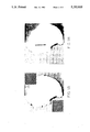
- FIGS. 1A-1F show a series of AFM images that depict the patterning of a MoO 3 crystallite with the letters "HU".
- FIGS. 2A-2E show a series of images of a MoO 3 crystallite on MoS 2 recorded with an applied load of 1 ⁇ 10 -8 N.
- FIG. 1a A typical image of MoO 3 crystallite formed after thermal oxidation of MoS 2 at 480° C. is shown in FIG. 1a.
- the MoO 3 has a thickness of ca. 15 ⁇ (corresponding to one unit cell along b) and occupies most of the central portion of this 500 ⁇ 500 nm 2 image.
- the MoO 3 and MoS 2 surfaces are stable to repetitive scanning when the imaging force is ⁇ 10 -8 N.
- FIG. 1B we show an image of the same area of the surface acquired after machining a line in the MoO 3 thin film.
- the line has a resolution of ⁇ 10 nm at the MoO 3 surface and 5 nm at its bottom, and is approximately one unit cell deep (18).
- FIG. 1 A series of 500 ⁇ 500 nm 2 AFM images that depict the patterning of a MoO 3 crystallite with the letters "HU". All of the images were recorded with an applied load of 1 ⁇ 10 -8 N.
- the insets shown in the lower and upper corners of this figure are atomic resolution images (3.5 ⁇ 3.5 nm 2 ) recorded on the MoS 2 and MoO 3 areas, respectively; the lattice parameters and symmetry of these images confirm the material assignment (see text).
- (B) A line machined in the MoO 3 crystal using an applied load of 5 ⁇ 10 -8 N.
- (C) Zoomed view of this structure rendered as a three dimensional line scan. A single scan across the line is also shown in the upper portion of this image.
- (D- F) 500 ⁇ 500 nm 2 images illustrating sequential machining of the MoO 3 crystallite to define the HU pattern.
- the white bar in (A) represents 50 nm and defines the length scale for A,B,D-F.
- FIG. 2. A series of 450 ⁇ 450 nm 2 images of a MoO 3 crystallite on MoS 2 recorded with an applied load of 1 ⁇ 10 -8 N. Two lines were machined through the left side of the MoO 3 (using a load of 1 ⁇ 10 -7 N) to define a triangular object (C). The white bar in (A) corresponds to 45 nm and defines the length scale for A-C.
Abstract
An atomic force microscope (AFM) has been used to machine complex patterns and to form free structural objects in thin layers of MoO3 grown on the surface of MoS2. The AFM tip can pattern lines with ≦10 nm resolution and then image the resulting structure without perturbation by controlling the applied load. Distinct MoO3 structures can also be defined by AFM machining, and furthermore, these objects can be manipulated on the MoS2 substrate surface using the AFM tip. These results suggest application to nanometer scale diffraction gratings, high-resolution lithography masks, and possibly the assembly of nanostructures with novel properties.
Description
The ability to manipulate matter and to assemble novel structures on the atomic to nanometer scale is currently a goal of many researchers in the physical and engineering sciences (1-15). One attractive strategy for achieving this goal is to use scanning probe microscopes, such as the scanning tunneling microscope (STM) or atomic force microscope (AFM), to move atoms or clusters of atoms directly into a desired configuration. For example, the STM has been used to remove single atoms from surfaces (2,3), to position atoms on a surface (4, 5), and to create an atomic switch (6). On a nanometer scale the STM has also been used to create structures by field-assisted diffusion (5,7), to develop organic resists (8), to expose passivated semiconductor surfaces (9), and to deposit gold islands on gold surfaces (10). Most recently researchers have utilized the STM to induce the dissociation of a single molecule on a silicon surface (11). In contrast, there are few examples of controlled, highresolution manipulation using the AFM. Several groups have shown that direct contact (repulsive mode) imaging of soft organic layers under sufficiently high loads can lead to orientational ordering of the organic and/or removal of this layer from the area scanned by the AFM tip (12, 13). The length-scale or resolution of these modifications typically has been ≧100 nm. In addition, AFM tip-induced wear of transition metal dichalogenide materials has been reported (14,15) on a ≧50 nm scale. The results from these AFM studies are promising, however, the resolution and control of the surface features produced by the AFM are poor compared to structures created with the STM.
We believe that the materials used in these previous AFM studies have significantly limited the attainable resolution and selectivity. Hence, we have sought to explore the limits of direct surface manipulation with the AFM using a novel material system that consists of a thin (<50 Å) metal oxide film (MoO3) on the surface of MoS2. In comparison to previous studies, this system has several unique features, including: (1) the thin MoO3 film is rigid and nondeformable in contrast to organic layers; (2) MoO3 can be selectively machined or imaged depending on the applied load of the AFM cantilever, and (3) the MoS2 substrate, which is a good lubricant, functions as an integral stop layer that automatically fixes the depth of the structures. Using this system we demonstrate herein controlled pattern development with ≦10 nm resolution, and complex machining of movable objects that have nanometer dimensions. The generalization of these results to other materials and their potential applications to nanotechnologics are discussed.
This crystallites of α-MoO3 were grown on the surface of single-crystal 2H-MoS2 by thermal oxidation using purified O2 at 480° C. for 5-10 minutes. The MoO3 layers were identified by transmission electron diffraction, X ray photoemission spectroscopy, and atomic resolution AFM images (16). These studies have shown that α-MoO3 (space-group Pbnm) grows with the b-axis (13.848 Å) perpendicular to the MoS2 substrate surface. For the above oxidation conditions MoO3 crystallics 1-3 unit cells thick (1-unit cell-b-axis=13.85 Å) and 200-500 nm on edge are formed. Additional details of the MoS2 oxidation process and the characterization of the MoO3 thin crystal layers will be discussed in detail elsewhere (16). All of the AFM experiments were carried out using a modified commercial instrument (Nanoscope, Digital Instruments, Inc.). Si3 N4 cantilever/tips (k≃0.38 N/m) were used for imaging and modification. In addition, the AFM experiments were carried out in nitrogen filled glove box equipped with a purification system that reduced the concentrations of oxygen and water to less than 5 ppm and 2 ppm, respectively. This environment enables us to obtain the reproducible conditions needed for controlled surface modification (17).
FIGS. 1A-1F show a series of AFM images that depict the patterning of a MoO3 crystallite with the letters "HU".
FIGS. 2A-2E show a series of images of a MoO3 crystallite on MoS2 recorded with an applied load of 1×10⁻⁸ N.
A typical image of MoO3 crystallite formed after thermal oxidation of MoS2 at 480° C. is shown in FIG. 1a. The MoO3 has a thickness of ca. 15 Å (corresponding to one unit cell along b) and occupies most of the central portion of this 500×500 nm2 image. Atomic-resolution images confirm this structural assignments: the a-c plane of MoO3 has orthorhombic symmetry, a=3.97 Å, and c=3.70 Å, and the (0001) surface of MoS2 has hexagonal symmetry, a=3.16 Å (insets, FIG. 1A). In addition, it is important to note that the MoO3 and MoS2 surfaces are stable to repetitive scanning when the imaging force is ≦10-8 N.
However, when the applied force is increased to ≧5×10⁻⁸ N we find that the MoO3 surface can be machined in a controlled manner with high-resolution. In FIG. 1B we show an image of the same area of the surface acquired after machining a line in the MoO3 thin film. The line has a resolution of ≃10 nm at the MoO3 surface and 5 nm at its bottom, and is approximately one unit cell deep (18). These features are shown clearly in a 3-dimensional line scan image and cross-sectional view (FIG. 1C). From this latter data it is also clear that the structure is microscopically very smooth. In addition, we find that continued scanning does not lead to features deeper than the thickness of the MoO3 thin-layer. It is thus apparent that the MoS2 substrate, which is a good solid lubricant, functions as a self-limiting stop in this modification process. We believe that the mechanism by which this structure is created is simply tip-induced wear of the MoO3 surface. Our experimental data strongly supports this mechanistic assignment since we find that the rate of structure formation is proportional to the applied load (≧5×10⁻⁸ N) and to the scan rate (35-470 nm/s). Furthermore, the cross-section of the line (FIG. 1C) matches the Si3 N4 tip shape determined by electron microscopy. In analogy to macroscopic processes, this tip-induced wear can be termed "nanomachining".
An important criteria for any reliable and potentially practical machining process is that the cutting tool (in our case the AFM tip) undergoes minimal wear compared to the substrate. To examine this issue and to determine the complexity and reproducibility of the patterns that can be created we have nanomachined a series of lines to pattern "H U", which stands for Harvard University, in the MoO3 (FIGS. 1D-1F). Importantly, we find that the resolution does not degrade during this series of nanomachining operations. In addition, the resulting HU structure is stable during continuous imaging with loads ≦10-8 N. Our work thus demonstrates that it is possible to create complex, durable, and high-resolution patterns in the MoO3 thin layers. There are several applications that one can envision with this system. First, it is possible using our technology to fabricate nanometer resolution diffraction gratings. The length of the grating lines would not be limited to the size of the crystallites produced by oxidation since it is possible to deposit uniform crystallinc films of MoO3 on MoS2 using laser ablation (19). It also will be interesting to consider using patterned MoO3 films as masks for high-resolution X-ray lithography. In a more general sense, it should be possible to utilize these ideas for nanomachining other inorganic thin layers, such as SiOx on Si, when the substrate (e.g., Si) wears at a rate significantly slower than the inorganic coating (e.g., SiOx) [20].
We can also go beyond the level of simply patterning a surface and make distinct objects that can be manipulated and in principle incorporated into complex nanostructures. The basis for this new idea is the fact that the MoO3 crystallites are not strongly bound to the underlying MoS2 substrate; therefore, it is possible to separate nanomachined MoO3 objects from the MoS2 surface. This concept is demonstrated in FIG. 2. In this series of AFM images we first define a triangle at the edge of a MoO3 crystallite (FIG. 2A-C). The line pattern defining the triangle was machined using a force of 1×10⁻⁷ N (21). The most remarkable feature of this series images is that the triangular structure patterned at the edge of the MoO3 can be separated from the original crystallite by scanning across the entire crystal with a force of ≃1×10⁻⁷ N (FIG. 2D). In FIG. 2D the triangular object was moved ≃100 nm after a single high load scan. We can further manipulate the triangular MoO3 object on the MoS2 using this procedure, and show a second ≃100 nm translation step in FIG. 2E. Importantly, these translation steps can be imaged without perturbation by using low loads (≦10-8 N). Hence, we are not only able to nanomachine free objects, but we can also translate and observe these objects on the MoS2 surface using an AFM tip. The objects we create and manipulate with the AFM are several orders of magnitude smaller than those currently produced by micromachining techniques (22). For future applications it is important to note that the electronic properties of MoO3 can be readily varied from insulating through metallic by doping, and that MoO3 and related metal oxides exhibit photochomism. Because it should be possible to lift these small objects electrostatically with the tip (in addition to translating them), it is interesting to speculate whether one can assemble nanostructures possessing novel electrical and optical properties using these techniques.
References and Notes
1. For recent reviews see: Science 254, 1300-1342 (1991); P. Ball and L. Garwin, Nature 355, 761 (1992).
2. I. W. Lyo and Ph. Avouris, Science 253, 173 (1991).
3. D. Cleary, New Sci. 129, 31 (1991); J. L. Huang, Y. E. Sung, C. M. Lieber, submitted for publication.
4. D. M. Eigler and E. D. Schweizer, Nature 344, 524 (1990).
5. J. A. Stroscio and D. M. Eigler, Science 254, 1319 (1991).
6. D. M. Eigler, C. P. Lutz, W. E. Rudge, Nature 352, 600 (1991).
7. L. J. Whitman, J. A. Stroscio, R. A. Dragoset, R. J. Celotta, Science 251, 1206 (1991).
8. C. R. K. Marrian, E. A. Dobisz, R. J. Colton, J. Vac. Sci. Technol. A 8, 3563 (1990); E. A. Dobisz and C. R. K. Marrian, Appl. Phys. Lett. 58, 2526 (1991).
9. J. A. Dagata et al., Appl. Phys. Lett. 56, 2001 (1990).
10. H. J. Mamin, S. Chiang, H. Birk, P. H. Guethner, D. Rugar, J. Vac. Sci. Technol. B 9, 1398 (1991).
11. G. Dujardin, R. E. Walkup, Ph. Avouris, Science 255, 1232 (1992).
12. G. S. Blackman, C. M. Mate, M. R. Philpott, Vacuum 41, 1283 (1990).
13. O. M. Leung and M. C. Goh, Science 255, 64 (1992).
14. Y. Kim, J.-L. Huang, C. M. Lieber, Appl. Phys. Lett. 59, 3404 (1991).
15. E. Delawski and B. A. Parkinson, J. Am. Chem. Soc. 114, 1661 (1992).
16. Y. Kim and C. M. Lieber, in preparation.
17. In air, the MoO3 and MoS2 surfaces wear in an uncontrolled manner. A strong adhesive interaction between the tip and sample, which is due to adsorbates, is believed to be responsible in large part for this observed wear. With the glove box, however, the MoS2 surface does not wear on our experimental time scale, and the wear of the MoO3 can be controlled by the applied load.
18. Lines with similar widths but only 3 Å deep have been formed previously in the metallic oxide Rb.sub..3 MoO3 by an unknown process using an STM: E. Garfunkel et al., Science 246, 99 (1989).
19. C. Niu and C. M. Lieber, unpublished results.
20. A stable tip is required to obtain reproducible nanomachining. For other oxide systems the Si3 N4 tips may not be sufficiently robust; however, cantilevers with diamond tips should be applicable to a wide range of materials.
21. The line resolution at the surface of the MoO3 is lower than in FIG. 1 since this crystallite is three times thicker (42 Å) than the one unit cell thick MoO3 layer patterned with HU.
22. K. D. Wise and K. Najafi, Science 254, 1335 (1991).
23. C.M.L. acknowledges support of this work by the Air Force Office of Scientific Research and the David and Lucile Packard Foundation. Y. K. dedicates this work to Professor S. J. Kim on the occasion of his 60th birthday.
Figure Captions.
FIG. 1. A series of 500×500 nm2 AFM images that depict the patterning of a MoO3 crystallite with the letters "HU". All of the images were recorded with an applied load of 1×10⁻⁸ N. (A) 500×500 nm2 image of MoO3 grown on the surface of a MoS2 single crystal. The irregular shaped object occupying the central portion of this image is the MoO3 crystallite and the surrounding regions correspond to the MoS2 substrate. The insets shown in the lower and upper corners of this figure are atomic resolution images (3.5×3.5 nm2) recorded on the MoS2 and MoO3 areas, respectively; the lattice parameters and symmetry of these images confirm the material assignment (see text). (B) A line machined in the MoO3 crystal using an applied load of 5×10⁻⁸ N. (C) Zoomed view of this structure rendered as a three dimensional line scan. A single scan across the line is also shown in the upper portion of this image. (D- F) 500×500 nm2 images illustrating sequential machining of the MoO3 crystallite to define the HU pattern. The white bar in (A) represents 50 nm and defines the length scale for A,B,D-F.
FIG. 2. (A-C) A series of 450×450 nm2 images of a MoO3 crystallite on MoS2 recorded with an applied load of 1×10⁻⁸ N. Two lines were machined through the left side of the MoO3 (using a load of 1×10⁻⁷ N) to define a triangular object (C). The white bar in (A) corresponds to 45 nm and defines the length scale for A-C. (D,E) 600×600 nm2 images that illustrate the translation of the triangular MoO3 structure on the MoS2 surface. In (D) the triangle has been moved≃100 nm from its position in (C). It was translated an additional 100 nm before recording image (E). Images D and E were recorded with an applied load of 1×10⁻⁸ N; translation was carried out using a higher load, 1×10⁻⁷ N. The white bar in (D) corresponds to 60 nm and defines the length scale for D and E.
Claims (1)
1. A method for machining oxide thin-films, comprising the steps of:
a) employing an atomic force microscope to pattern lines on the oxide thin film; and
b) imaging a resulting structure by controlling an applied load of a tip of the atomic force microscope.
Priority Applications (1)
| Application Number | Priority Date | Filing Date | Title |
|---|---|---|---|
| US07/916,215 US5252835A (en) | 1992-07-17 | 1992-07-17 | Machining oxide thin-films with an atomic force microscope: pattern and object formation on the nanometer scale |
Applications Claiming Priority (1)
| Application Number | Priority Date | Filing Date | Title |
|---|---|---|---|
| US07/916,215 US5252835A (en) | 1992-07-17 | 1992-07-17 | Machining oxide thin-films with an atomic force microscope: pattern and object formation on the nanometer scale |
Publications (1)
| Publication Number | Publication Date |
|---|---|
| US5252835A true US5252835A (en) | 1993-10-12 |
Family
ID=25436890
Family Applications (1)
| Application Number | Title | Priority Date | Filing Date |
|---|---|---|---|
| US07/916,215 Expired - Fee Related US5252835A (en) | 1992-07-17 | 1992-07-17 | Machining oxide thin-films with an atomic force microscope: pattern and object formation on the nanometer scale |
Country Status (1)
| Country | Link |
|---|---|
| US (1) | US5252835A (en) |
Cited By (107)
| Publication number | Priority date | Publication date | Assignee | Title |
|---|---|---|---|---|
| US5365073A (en) * | 1992-06-24 | 1994-11-15 | Hitachi, Ltd. | Nanofabricated structures |
| US5561300A (en) * | 1991-12-24 | 1996-10-01 | Hitachi, Ltd. | Atomic switching devices and logical circuits |
| US5831181A (en) * | 1995-09-29 | 1998-11-03 | The Regents Of The University Of California | Automated tool for precision machining and imaging |
| US5874668A (en) * | 1995-10-24 | 1999-02-23 | Arch Development Corporation | Atomic force microscope for biological specimens |
| US5962863A (en) * | 1993-09-09 | 1999-10-05 | The United States Of America As Represented By The Secretary Of The Navy | Laterally disposed nanostructures of silicon on an insulating substrate |
| US6099945A (en) * | 1996-04-11 | 2000-08-08 | Nec Corporation | Atomic mask and method of patterning a substrate with the atomic mask |
| CN1056164C (en) * | 1996-06-25 | 2000-09-06 | 华南理工大学 | Method for preparing high electric-activity conductive bending-resistant nanometre compound film |
| US6218086B1 (en) * | 1997-07-17 | 2001-04-17 | International Business Machines Corporation | Method of forming ultrasmall structures and apparatus therefor |
| US6322938B1 (en) * | 2000-05-22 | 2001-11-27 | The United States Of America As Represented By The Secretary Of The Air Force | Nanolithography for multi-passband grating filters |
| US20020063212A1 (en) * | 1999-01-07 | 2002-05-30 | Mirkin Chad A. | Methods utilizing scanning probe microscope tips and products therefor or produced thereby |
| US20020125427A1 (en) * | 2001-03-09 | 2002-09-12 | Veeco Instruments Inc. | Method and apparatus for manipulating a sample |
| WO2002073624A2 (en) * | 2001-03-13 | 2002-09-19 | Paul Scherrer Institut (Psi) | Memory element, method for structuring a surface, and storage device |
| US20030077661A1 (en) * | 2002-11-27 | 2003-04-24 | Kastan Michael B. | ATM kinase compositions and methods |
| EP1312443A2 (en) * | 2001-11-16 | 2003-05-21 | National Institute of Advanced Industrial Science and Technology | Method of levelling depressed surfaces of organic crystals |
| US6574130B2 (en) | 2001-07-25 | 2003-06-03 | Nantero, Inc. | Hybrid circuit having nanotube electromechanical memory |
| US6635311B1 (en) | 1999-01-07 | 2003-10-21 | Northwestern University | Methods utilizing scanning probe microscope tips and products therefor or products thereby |
| US6643165B2 (en) | 2001-07-25 | 2003-11-04 | Nantero, Inc. | Electromechanical memory having cell selection circuitry constructed with nanotube technology |
| US20040005723A1 (en) * | 2002-04-02 | 2004-01-08 | Nanosys, Inc. | Methods of making, positioning and orienting nanostructures, nanostructure arrays and nanostructure devices |
| US20040026684A1 (en) * | 2002-04-02 | 2004-02-12 | Nanosys, Inc. | Nanowire heterostructures for encoding information |
| US6706402B2 (en) | 2001-07-25 | 2004-03-16 | Nantero, Inc. | Nanotube films and articles |
| US20040146560A1 (en) * | 2002-09-05 | 2004-07-29 | Nanosys, Inc. | Oriented nanostructures and methods of preparing |
| US6784028B2 (en) | 2001-12-28 | 2004-08-31 | Nantero, Inc. | Methods of making electromechanical three-trace junction devices |
| US20040209047A1 (en) * | 2003-04-15 | 2004-10-21 | Extrand Charles W. | Microfluidic device with ultraphobic surfaces |
| US20040206448A1 (en) * | 2003-04-17 | 2004-10-21 | Nanosys, Inc. | Structures, systems and methods for joining articles and materials and uses therefor |
| US20040206662A1 (en) * | 2003-04-15 | 2004-10-21 | Extrand Charles W. | Tray carrier with ultraphobic surfaces |
| US20040206410A1 (en) * | 2003-04-15 | 2004-10-21 | Entegris, Inc. | Fluid handling component with ultraphobic surfaces |
| US20040206663A1 (en) * | 2003-04-15 | 2004-10-21 | Entegris, Inc. | Carrier with ultraphobic surfaces |
| US20040209139A1 (en) * | 2003-04-15 | 2004-10-21 | Entegris, Inc. | Fuel cell with ultraphobic surfaces |
| US20040208791A1 (en) * | 2003-04-15 | 2004-10-21 | Entegris, Inc. | Ultraphobic surface for high pressure liquids |
| US20040250950A1 (en) * | 2003-04-17 | 2004-12-16 | Nanosys, Inc. | Structures, systems and methods for joining articles and materials and uses therefor |
| US20040256311A1 (en) * | 2003-04-15 | 2004-12-23 | Extrand Charles W. | Ultralyophobic membrane |
| US6835591B2 (en) | 2001-07-25 | 2004-12-28 | Nantero, Inc. | Methods of nanotube films and articles |
| US20050006673A1 (en) * | 2003-04-04 | 2005-01-13 | Btg International Limited | Nanowhiskers with PN junctions, doped nanowhiskers, and methods for preparing them |
| US20050011431A1 (en) * | 2003-04-04 | 2005-01-20 | Btg International Limited | Precisely positioned nanowhiskers and nanowhisker arrays and method for preparing them |
| US20050017171A1 (en) * | 2003-07-08 | 2005-01-27 | Btg International Limited | Probe structures incorporating nanowhiskers, production methods thereof and methods of forming nanowhiskers |
| US20050038498A1 (en) * | 2003-04-17 | 2005-02-17 | Nanosys, Inc. | Medical device applications of nanostructured surfaces |
| US6911682B2 (en) | 2001-12-28 | 2005-06-28 | Nantero, Inc. | Electromechanical three-trace junction devices |
| US6919592B2 (en) | 2001-07-25 | 2005-07-19 | Nantero, Inc. | Electromechanical memory array using nanotube ribbons and method for making same |
| US20050181195A1 (en) * | 2003-04-28 | 2005-08-18 | Nanosys, Inc. | Super-hydrophobic surfaces, methods of their construction and uses therefor |
| US20050208268A1 (en) * | 2003-04-15 | 2005-09-22 | Extrand Charles W | Article with ultraphobic surface |
| US20050219788A1 (en) * | 2004-03-18 | 2005-10-06 | Nanosys, Inc. | Nanofiber surface based capacitors |
| US20050221072A1 (en) * | 2003-04-17 | 2005-10-06 | Nanosys, Inc. | Medical device applications of nanostructured surfaces |
| US20050279274A1 (en) * | 2004-04-30 | 2005-12-22 | Chunming Niu | Systems and methods for nanowire growth and manufacturing |
| US20060008942A1 (en) * | 2004-07-07 | 2006-01-12 | Nanosys, Inc. | Systems and methods for harvesting and integrating nanowires |
| US20060019470A1 (en) * | 2004-02-06 | 2006-01-26 | Btg International Limited | Directionally controlled growth of nanowhiskers |
| US20060019472A1 (en) * | 2004-04-30 | 2006-01-26 | Nanosys, Inc. | Systems and methods for nanowire growth and harvesting |
| US6998689B2 (en) | 2002-09-09 | 2006-02-14 | General Nanotechnology Llc | Fluid delivery for scanning probe microscopy |
| US7035308B1 (en) | 2002-10-28 | 2006-04-25 | Science Applications International Corporation | Method and system for countering laser technology |
| US7042828B2 (en) | 1995-07-24 | 2006-05-09 | General Nanotechnology Llc | Nanometer scale data storage device and associated positioning system |
| US7045780B2 (en) | 1994-07-28 | 2006-05-16 | General Nanotechnology, Llc | Scanning probe microscopy inspection and modification system |
| US20060122596A1 (en) * | 2003-04-17 | 2006-06-08 | Nanosys, Inc. | Structures, systems and methods for joining articles and materials and uses therefor |
| US20060125056A1 (en) * | 2004-06-25 | 2006-06-15 | Btg International Limited | Formation of nanowhiskers on a substrate of dissimilar material |
| US20060159916A1 (en) * | 2003-05-05 | 2006-07-20 | Nanosys, Inc. | Nanofiber surfaces for use in enhanced surface area applications |
| US20060204738A1 (en) * | 2003-04-17 | 2006-09-14 | Nanosys, Inc. | Medical device applications of nanostructured surfaces |
| US7109482B2 (en) | 1999-07-01 | 2006-09-19 | General Nanotechnology Llc | Object inspection and/or modification system and method |
| US20060240218A1 (en) * | 2005-04-26 | 2006-10-26 | Nanosys, Inc. | Paintable nonofiber coatings |
| US7129554B2 (en) | 2000-12-11 | 2006-10-31 | President & Fellows Of Harvard College | Nanosensors |
| US7176505B2 (en) | 2001-12-28 | 2007-02-13 | Nantero, Inc. | Electromechanical three-trace junction devices |
| US7178387B1 (en) | 2001-03-08 | 2007-02-20 | General Nanotechnology Llc | Method and apparatus for scanning in scanning probe microscopy and presenting results |
| US7196328B1 (en) * | 2001-03-08 | 2007-03-27 | General Nanotechnology Llc | Nanomachining method and apparatus |
| US7211464B2 (en) | 2000-08-22 | 2007-05-01 | President & Fellows Of Harvard College | Doped elongated semiconductors, growing such semiconductors, devices including such semiconductors and fabricating such devices |
| US7254151B2 (en) | 2002-07-19 | 2007-08-07 | President & Fellows Of Harvard College | Nanoscale coherent optical components |
| US20070190880A1 (en) * | 2004-02-02 | 2007-08-16 | Nanosys, Inc. | Porous substrates, articles, systems and compositions comprising nanofibers and methods of their use and production |
| US20070206488A1 (en) * | 2006-02-23 | 2007-09-06 | Claes Thelander | Data storage nanostructures |
| US7266998B2 (en) | 2001-11-28 | 2007-09-11 | General Nanotechnology Llc | Method and apparatus for micromachines, microstructures, nanomachines and nanostructures |
| US7274078B2 (en) | 2001-07-25 | 2007-09-25 | Nantero, Inc. | Devices having vertically-disposed nanofabric articles and methods of making the same |
| US7301199B2 (en) | 2000-08-22 | 2007-11-27 | President And Fellows Of Harvard College | Nanoscale wires and related devices |
| US7304357B2 (en) | 2001-07-25 | 2007-12-04 | Nantero, Inc. | Devices having horizontally-disposed nanofabric articles and methods of making the same |
| US20070282247A1 (en) * | 2003-05-05 | 2007-12-06 | Nanosys, Inc. | Medical Device Applications of Nanostructured Surfaces |
| US20070296032A1 (en) * | 2004-09-16 | 2007-12-27 | Nanosys, Inc. | Artificial dielectrics using nanostructures |
| US20080038520A1 (en) * | 2005-12-29 | 2008-02-14 | Nanosys, Inc. | Methods for oriented growth of nanowires on patterned substrates |
| CN100370216C (en) * | 2005-12-20 | 2008-02-20 | 西安交通大学 | Nano Line width sample plate and its preparation method |
| US7335908B2 (en) | 2002-07-08 | 2008-02-26 | Qunano Ab | Nanostructures and methods for manufacturing the same |
| US7335395B2 (en) | 2002-04-23 | 2008-02-26 | Nantero, Inc. | Methods of using pre-formed nanotubes to make carbon nanotube films, layers, fabrics, ribbons, elements and articles |
| US20080149944A1 (en) * | 2006-12-22 | 2008-06-26 | Qunano Ab | Led with upstanding nanowire structure and method of producing such |
| US20080149914A1 (en) * | 2006-12-22 | 2008-06-26 | Qunano Ab | Nanoelectronic structure and method of producing such |
| CN100408970C (en) * | 2006-06-30 | 2008-08-06 | 西安交通大学 | Nano multi-step height sample plate and its preparation |
| US20080202221A1 (en) * | 1994-07-28 | 2008-08-28 | General Nanotechnology Llc | Methods and apparatus for nanolapping |
| WO2008118399A1 (en) * | 2007-03-26 | 2008-10-02 | University Of Pittsburgh - Of The Commonwealth System Of Higher Education | Ultrahigh density patterning of conducting media |
| US20090127540A1 (en) * | 2006-11-07 | 2009-05-21 | Nanosys, Inc. | Systems and Methods for Nanowire Growth |
| US20090143227A1 (en) * | 2004-02-02 | 2009-06-04 | Nanosys, Inc. | Porous substrates, articles, systems and compositions comprising nanofibers and methods of their use and production |
| US7560136B2 (en) | 2003-01-13 | 2009-07-14 | Nantero, Inc. | Methods of using thin metal layers to make carbon nanotube films, layers, fabrics, ribbons, elements and articles |
| US7566478B2 (en) | 2001-07-25 | 2009-07-28 | Nantero, Inc. | Methods of making carbon nanotube films, layers, fabrics, ribbons, elements and articles |
| US20090192429A1 (en) * | 2007-12-06 | 2009-07-30 | Nanosys, Inc. | Resorbable nanoenhanced hemostatic structures and bandage materials |
| US7615738B2 (en) | 1994-07-28 | 2009-11-10 | General Nanotechnology, Llc | Scanning probe microscope assembly and method for making spectrophotometric, near-field, and scanning probe measurements |
| US20100148149A1 (en) * | 2006-12-22 | 2010-06-17 | Qunano Ab | Elevated led and method of producing such |
| US7741197B1 (en) | 2005-12-29 | 2010-06-22 | Nanosys, Inc. | Systems and methods for harvesting and reducing contamination in nanowires |
| US20100173070A1 (en) * | 2004-02-02 | 2010-07-08 | Nanosys, Inc. | Porous Substrates, Articles, Systems and Compositions Comprising Nanofibers and Methods of Their Use and Production |
| US7785922B2 (en) | 2004-04-30 | 2010-08-31 | Nanosys, Inc. | Methods for oriented growth of nanowires on patterned substrates |
| US20100283064A1 (en) * | 2006-12-22 | 2010-11-11 | Qunano Ab | Nanostructured led array with collimating reflectors |
| US20100297502A1 (en) * | 2009-05-19 | 2010-11-25 | Nanosys, Inc. | Nanostructured Materials for Battery Applications |
| US20100304491A1 (en) * | 2002-09-26 | 2010-12-02 | Mcneil Scott Earl | Method and System For Detection Using Nanodot Taggants |
| US7858965B2 (en) | 2005-06-06 | 2010-12-28 | President And Fellows Of Harvard College | Nanowire heterostructures |
| US20110064785A1 (en) * | 2007-12-06 | 2011-03-17 | Nanosys, Inc. | Nanostructure-Enhanced Platelet Binding and Hemostatic Structures |
| US7968474B2 (en) | 2006-11-09 | 2011-06-28 | Nanosys, Inc. | Methods for nanowire alignment and deposition |
| US20110165337A1 (en) * | 2007-05-07 | 2011-07-07 | Nanosys, Inc. | Method and system for printing aligned nanowires and other electrical devices |
| US20110165405A1 (en) * | 2004-09-16 | 2011-07-07 | Nanosys, Inc. | Continuously variable graded artificial dielectrics using nanostructures |
| US8058640B2 (en) | 2006-09-11 | 2011-11-15 | President And Fellows Of Harvard College | Branched nanoscale wires |
| US8154002B2 (en) | 2004-12-06 | 2012-04-10 | President And Fellows Of Harvard College | Nanoscale wire-based data storage |
| US20120113242A1 (en) * | 2000-05-03 | 2012-05-10 | Aperio Technologies, Inc. | Data Management in a Linear-Array-Based Microscope Slide Scanner |
| US8232584B2 (en) | 2005-05-25 | 2012-07-31 | President And Fellows Of Harvard College | Nanoscale sensors |
| US8540889B1 (en) | 2008-11-19 | 2013-09-24 | Nanosys, Inc. | Methods of generating liquidphobic surfaces |
| US8558311B2 (en) | 2004-09-16 | 2013-10-15 | Nanosys, Inc. | Dielectrics using substantially longitudinally oriented insulated conductive wires |
| US8575663B2 (en) | 2006-11-22 | 2013-11-05 | President And Fellows Of Harvard College | High-sensitivity nanoscale wire sensors |
| US9102521B2 (en) | 2006-06-12 | 2015-08-11 | President And Fellows Of Harvard College | Nanosensors and related technologies |
| US9297796B2 (en) | 2009-09-24 | 2016-03-29 | President And Fellows Of Harvard College | Bent nanowires and related probing of species |
| US9390951B2 (en) | 2009-05-26 | 2016-07-12 | Sharp Kabushiki Kaisha | Methods and systems for electric field deposition of nanowires and other devices |
-
1992
- 1992-07-17 US US07/916,215 patent/US5252835A/en not_active Expired - Fee Related
Non-Patent Citations (26)
| Title |
|---|
| Dagata et al., "Modification of Hydrogen-Passivated Silicon by a Scanning Tunneling Microscope Operating in Air", Appl. Phys. Lett., 56(20):2001-2003 (1990). |
| Dagata et al., Modification of Hydrogen Passivated Silicon by a Scanning Tunneling Microscope Operating in Air , Appl. Phys. Lett., 56(20):2001 2003 (1990). * |
| Delawski et al., "Layer-by-Layer Etching of Two-Dimentional Metal Chalcogenides with the Atomic Force Microscope", J. Am. Chem. Soc., 114(5):1661-1667 (1992). |
| Delawski et al., Layer by Layer Etching of Two Dimentional Metal Chalcogenides with the Atomic Force Microscope , J. Am. Chem. Soc., 114(5):1661 1667 (1992). * |
| Dobisz et al., "Sub-30 nm Lithography in a Negative Electron Beam Resist with a Vacuum Scanning Tunneling Microscope", Appl. Phys. Lett., 58(22):2526-2528 (1991). |
| Dobisz et al., Sub 30 nm Lithography in a Negative Electron Beam Resist with a Vacuum Scanning Tunneling Microscope , Appl. Phys. Lett., 58(22):2526 2528 (1991). * |
| Dujardin et al., "Dissociation of Individual Molecules with Electrons from the Tip of a Scanning Tunneling Microscope", Science, 255, 1232-1235 (1992). |
| Dujardin et al., Dissociation of Individual Molecules with Electrons from the Tip of a Scanning Tunneling Microscope , Science, 255, 1232 1235 (1992). * |
| Eigler et al., "An Atomic Switch Realized with the Scanning Tunnelling Microscope", Nature, 352, 600-603 (1991). |
| Eigler et al., An Atomic Switch Realized with the Scanning Tunnelling Microscope , Nature, 352, 600 603 (1991). * |
| Garfunkel et al., "Scanning Tunneling Microscopy and Nanolithography on a Conducting Oxide, Rb0.3 MoO3 ", Science, 246 99-100 (1989). |
| Garfunkel et al., Scanning Tunneling Microscopy and Nanolithography on a Conducting Oxide, Rb 0.3 MoO 3 , Science, 246 99 100 (1989). * |
| Kim et al., "Characterization of nanometer scale wear and oxidation of transition metal dichalcogenide lubricants by atomic force microscopy", Appl. Phys. Lett., 59(26):3404-3406 (1991). |
| Kim et al., Characterization of nanometer scale wear and oxidation of transition metal dichalcogenide lubricants by atomic force microscopy , Appl. Phys. Lett., 59(26):3404 3406 (1991). * |
| Leung et al., "Orientational Ordering of Polymers by Atomic Force Microscopr Tip-Surface Interaction", Science, 255 64-66 (1992). |
| Leung et al., Orientational Ordering of Polymers by Atomic Force Microscopr Tip Surface Interaction , Science, 255 64 66 (1992). * |
| Lyo et al., "Field-Induced Nanometer- to Atomic-Scale Manipulation of Silicon Surfaces with the STM", Science, 253, 173-176 (1991). |
| Lyo et al., Field Induced Nanometer to Atomic Scale Manipulation of Silicon Surfaces with the STM , Science, 253, 173 176 (1991). * |
| Mamin et al., "Gold Deposition from a Scanning Tunneling Microscope Tip", J. Vac. Sci. Technol., 9(2):1398-1402 (1991). |
| Mamin et al., Gold Deposition from a Scanning Tunneling Microscope Tip , J. Vac. Sci. Technol., 9(2):1398 1402 (1991). * |
| Mate et al., "Atomic Force Microscope Studies of Lubricant Films on Solid Surfaces", Vacuum, 41 1283-1286 (1990). |
| Mate et al., Atomic Force Microscope Studies of Lubricant Films on Solid Surfaces , Vacuum, 41 1283 1286 (1990). * |
| Whitman et al., Manipulation of Adsorbed Atoms and Creation of New Structures on Room Temperature Surfaces with a Scanning Tunneling Microscope , Science, 251, 1206 1210 (1991). * |
| Whitman et al.,"Manipulation of Adsorbed Atoms and Creation of New Structures on Room-Temperature Surfaces with a Scanning Tunneling Microscope", Science, 251, 1206-1210 (1991). |
| Wise et al., "Microfabrication Techniques for Integrated Sensors and Microsystems", Science, 254, 1335-1342 (1991). |
| Wise et al., Microfabrication Techniques for Integrated Sensors and Microsystems , Science, 254, 1335 1342 (1991). * |
Cited By (269)
| Publication number | Priority date | Publication date | Assignee | Title |
|---|---|---|---|---|
| US5561300A (en) * | 1991-12-24 | 1996-10-01 | Hitachi, Ltd. | Atomic switching devices and logical circuits |
| US5365073A (en) * | 1992-06-24 | 1994-11-15 | Hitachi, Ltd. | Nanofabricated structures |
| US5962863A (en) * | 1993-09-09 | 1999-10-05 | The United States Of America As Represented By The Secretary Of The Navy | Laterally disposed nanostructures of silicon on an insulating substrate |
| US7485856B2 (en) | 1994-07-28 | 2009-02-03 | General Nanotechnology Llp | Scanning probe microscopy inspection and modification system |
| US7045780B2 (en) | 1994-07-28 | 2006-05-16 | General Nanotechnology, Llc | Scanning probe microscopy inspection and modification system |
| US7615738B2 (en) | 1994-07-28 | 2009-11-10 | General Nanotechnology, Llc | Scanning probe microscope assembly and method for making spectrophotometric, near-field, and scanning probe measurements |
| US20080202221A1 (en) * | 1994-07-28 | 2008-08-28 | General Nanotechnology Llc | Methods and apparatus for nanolapping |
| US7535817B2 (en) | 1995-07-24 | 2009-05-19 | General Nanotechnology, L.L.C. | Nanometer scale data storage device and associated positioning system |
| US7042828B2 (en) | 1995-07-24 | 2006-05-09 | General Nanotechnology Llc | Nanometer scale data storage device and associated positioning system |
| US5831181A (en) * | 1995-09-29 | 1998-11-03 | The Regents Of The University Of California | Automated tool for precision machining and imaging |
| US5874668A (en) * | 1995-10-24 | 1999-02-23 | Arch Development Corporation | Atomic force microscope for biological specimens |
| US6099945A (en) * | 1996-04-11 | 2000-08-08 | Nec Corporation | Atomic mask and method of patterning a substrate with the atomic mask |
| CN1056164C (en) * | 1996-06-25 | 2000-09-06 | 华南理工大学 | Method for preparing high electric-activity conductive bending-resistant nanometre compound film |
| WO2004074765A1 (en) * | 1997-07-17 | 2004-09-02 | Gerd Karl Binnig | Method of forming ultrasmall structures and apparatus therefor |
| US6218086B1 (en) * | 1997-07-17 | 2001-04-17 | International Business Machines Corporation | Method of forming ultrasmall structures and apparatus therefor |
| US10610995B2 (en) | 1998-01-21 | 2020-04-07 | Victor B. Kley | Method and apparatus for nanolapping |
| US20040028814A1 (en) * | 1999-01-07 | 2004-02-12 | Northwestern University | Methods utilizing scanning probe microscope tips and products therefor or produced thereby |
| US6635311B1 (en) | 1999-01-07 | 2003-10-21 | Northwestern University | Methods utilizing scanning probe microscope tips and products therefor or products thereby |
| US8247032B2 (en) | 1999-01-07 | 2012-08-21 | Northwestern University | Methods utilizing scanning probe microscope tips and products therefor or produced thereby |
| US6827979B2 (en) | 1999-01-07 | 2004-12-07 | Northwestern University | Methods utilizing scanning probe microscope tips and products therefor or produced thereby |
| US7569252B2 (en) | 1999-01-07 | 2009-08-04 | Northwestern University | Methods utilizing scanning probe microscope tips and products therefor or produced thereby |
| US20020063212A1 (en) * | 1999-01-07 | 2002-05-30 | Mirkin Chad A. | Methods utilizing scanning probe microscope tips and products therefor or produced thereby |
| US20100040847A1 (en) * | 1999-01-07 | 2010-02-18 | Northwestern University | Methods utilizing scanning probe microscope tips and products therefor or produced thereby |
| US7109482B2 (en) | 1999-07-01 | 2006-09-19 | General Nanotechnology Llc | Object inspection and/or modification system and method |
| US8731260B2 (en) * | 2000-05-03 | 2014-05-20 | Leica Biosystems Imaging, Inc. | Data management in a linear-array-based microscope slide scanner |
| US9521309B2 (en) | 2000-05-03 | 2016-12-13 | Leica Biosystems Imaging, Inc. | Data management in a linear-array-based microscope slide scanner |
| US20120113242A1 (en) * | 2000-05-03 | 2012-05-10 | Aperio Technologies, Inc. | Data Management in a Linear-Array-Based Microscope Slide Scanner |
| US9729749B2 (en) | 2000-05-03 | 2017-08-08 | Leica Biosystems Imaging, Inc. | Data management in a linear-array-based microscope slide scanner |
| US6322938B1 (en) * | 2000-05-22 | 2001-11-27 | The United States Of America As Represented By The Secretary Of The Air Force | Nanolithography for multi-passband grating filters |
| US7915151B2 (en) | 2000-08-22 | 2011-03-29 | President And Fellows Of Harvard College | Doped elongated semiconductors, growing such semiconductors, devices including such semiconductors and fabricating such devices |
| US7476596B2 (en) | 2000-08-22 | 2009-01-13 | President And Fellows Of Harvard College | Doped elongated semiconductors, growing such semiconductors, devices including such semiconductors, and fabricating such devices |
| US7301199B2 (en) | 2000-08-22 | 2007-11-27 | President And Fellows Of Harvard College | Nanoscale wires and related devices |
| US7211464B2 (en) | 2000-08-22 | 2007-05-01 | President & Fellows Of Harvard College | Doped elongated semiconductors, growing such semiconductors, devices including such semiconductors and fabricating such devices |
| US7595260B2 (en) | 2000-08-22 | 2009-09-29 | President And Fellows Of Harvard College | Doped elongated semiconductors, growing such semiconductors, devices including such semiconductors, and fabricating such devices |
| US7666708B2 (en) | 2000-08-22 | 2010-02-23 | President And Fellows Of Harvard College | Doped elongated semiconductors, growing such semiconductors, devices including such semiconductors, and fabricating such devices |
| US8153470B2 (en) | 2000-08-22 | 2012-04-10 | President And Fellows Of Harvard College | Doped elongated semiconductors, growing such semiconductors, devices including such semiconductors, and fabricating such devices |
| US8399339B2 (en) | 2000-12-11 | 2013-03-19 | President And Fellows Of Harvard College | Nanosensors |
| US7385267B2 (en) | 2000-12-11 | 2008-06-10 | President And Fellows Of Harvard College | Nanosensors |
| US7129554B2 (en) | 2000-12-11 | 2006-10-31 | President & Fellows Of Harvard College | Nanosensors |
| US7911009B2 (en) | 2000-12-11 | 2011-03-22 | President And Fellows Of Harvard College | Nanosensors |
| US7956427B2 (en) | 2000-12-11 | 2011-06-07 | President And Fellows Of Harvard College | Nanosensors |
| US20080211040A1 (en) * | 2000-12-11 | 2008-09-04 | President And Fellows Of Harvard College | Nanosensors |
| US7619290B2 (en) | 2000-12-11 | 2009-11-17 | President And Fellows Of Harvard College | Nanosensors |
| US7256466B2 (en) | 2000-12-11 | 2007-08-14 | President & Fellows Of Harvard College | Nanosensors |
| US7178387B1 (en) | 2001-03-08 | 2007-02-20 | General Nanotechnology Llc | Method and apparatus for scanning in scanning probe microscopy and presenting results |
| US7196328B1 (en) * | 2001-03-08 | 2007-03-27 | General Nanotechnology Llc | Nanomachining method and apparatus |
| US7947952B1 (en) | 2001-03-08 | 2011-05-24 | General Nanotechnology Llc | Nanomachining method and apparatus |
| US6862921B2 (en) | 2001-03-09 | 2005-03-08 | Veeco Instruments Inc. | Method and apparatus for manipulating a sample |
| US20020125427A1 (en) * | 2001-03-09 | 2002-09-12 | Veeco Instruments Inc. | Method and apparatus for manipulating a sample |
| WO2002073624A2 (en) * | 2001-03-13 | 2002-09-19 | Paul Scherrer Institut (Psi) | Memory element, method for structuring a surface, and storage device |
| US20030133324A1 (en) * | 2001-03-13 | 2003-07-17 | Paul Scherrer Institut (Psi) | Memory element, method for structuring a surface, and storage device |
| WO2002073624A3 (en) * | 2001-03-13 | 2003-10-02 | Paul Scherrer Inst Psi | Memory element, method for structuring a surface, and storage device |
| US6819588B2 (en) | 2001-03-13 | 2004-11-16 | Paul Scherrer Institut (Psi) | Memory element, method for structuring a surface, and storage device |
| US7298016B2 (en) | 2001-07-25 | 2007-11-20 | Nantero, Inc. | Electromechanical memory array using nanotube ribbons and method for making same |
| US7342818B2 (en) | 2001-07-25 | 2008-03-11 | Nantero, Inc. | Hybrid circuit having nanotube electromechanical memory |
| US6919592B2 (en) | 2001-07-25 | 2005-07-19 | Nantero, Inc. | Electromechanical memory array using nanotube ribbons and method for making same |
| US7264990B2 (en) | 2001-07-25 | 2007-09-04 | Nantero, Inc. | Methods of nanotubes films and articles |
| US6942921B2 (en) | 2001-07-25 | 2005-09-13 | Nantero, Inc. | Nanotube films and articles |
| US7120047B2 (en) | 2001-07-25 | 2006-10-10 | Segal Brent M | Device selection circuitry constructed with nanotube technology |
| US6706402B2 (en) | 2001-07-25 | 2004-03-16 | Nantero, Inc. | Nanotube films and articles |
| US7304357B2 (en) | 2001-07-25 | 2007-12-04 | Nantero, Inc. | Devices having horizontally-disposed nanofabric articles and methods of making the same |
| US7335528B2 (en) | 2001-07-25 | 2008-02-26 | Nantero, Inc. | Methods of nanotube films and articles |
| US7566478B2 (en) | 2001-07-25 | 2009-07-28 | Nantero, Inc. | Methods of making carbon nanotube films, layers, fabrics, ribbons, elements and articles |
| US6574130B2 (en) | 2001-07-25 | 2003-06-03 | Nantero, Inc. | Hybrid circuit having nanotube electromechanical memory |
| US6643165B2 (en) | 2001-07-25 | 2003-11-04 | Nantero, Inc. | Electromechanical memory having cell selection circuitry constructed with nanotube technology |
| US7056758B2 (en) | 2001-07-25 | 2006-06-06 | Nantero, Inc. | Electromechanical memory array using nanotube ribbons and method for making same |
| US6835591B2 (en) | 2001-07-25 | 2004-12-28 | Nantero, Inc. | Methods of nanotube films and articles |
| US7745810B2 (en) | 2001-07-25 | 2010-06-29 | Nantero, Inc. | Nanotube films and articles |
| US7274078B2 (en) | 2001-07-25 | 2007-09-25 | Nantero, Inc. | Devices having vertically-disposed nanofabric articles and methods of making the same |
| US8101976B2 (en) | 2001-07-25 | 2012-01-24 | Nantero Inc. | Device selection circuitry constructed with nanotube ribbon technology |
| US6836424B2 (en) | 2001-07-25 | 2004-12-28 | Nantero, Inc. | Hybrid circuit having nanotube electromechanical memory |
| EP1312443A3 (en) * | 2001-11-16 | 2003-09-24 | National Institute of Advanced Industrial Science and Technology | Method of levelling depressed surfaces of organic crystals |
| EP1312443A2 (en) * | 2001-11-16 | 2003-05-21 | National Institute of Advanced Industrial Science and Technology | Method of levelling depressed surfaces of organic crystals |
| US20030096502A1 (en) * | 2001-11-16 | 2003-05-22 | Hiroshi Nanjo | Method for levelling depressed surface of organic crystals |
| US7266998B2 (en) | 2001-11-28 | 2007-09-11 | General Nanotechnology Llc | Method and apparatus for micromachines, microstructures, nanomachines and nanostructures |
| US7631549B1 (en) | 2001-11-28 | 2009-12-15 | General Nanotechnology Llc | Method and apparatus for micromachines, microstructures, nanomachines and nanostructures |
| US6911682B2 (en) | 2001-12-28 | 2005-06-28 | Nantero, Inc. | Electromechanical three-trace junction devices |
| US6979590B2 (en) | 2001-12-28 | 2005-12-27 | Nantero, Inc. | Methods of making electromechanical three-trace junction devices |
| US7915066B2 (en) | 2001-12-28 | 2011-03-29 | Nantero, Inc. | Methods of making electromechanical three-trace junction devices |
| US20040191978A1 (en) * | 2001-12-28 | 2004-09-30 | Nantero, Inc. | Methods of making electromechanical three-trace junction devices |
| US6784028B2 (en) | 2001-12-28 | 2004-08-31 | Nantero, Inc. | Methods of making electromechanical three-trace junction devices |
| US7176505B2 (en) | 2001-12-28 | 2007-02-13 | Nantero, Inc. | Electromechanical three-trace junction devices |
| US7521736B2 (en) | 2001-12-28 | 2009-04-21 | Nantero, Inc. | Electromechanical three-trace junction devices |
| US9075082B2 (en) | 2002-03-07 | 2015-07-07 | Victor B. Kley | Fluid delivery for scanning probe microscopy |
| US20050230356A1 (en) * | 2002-04-02 | 2005-10-20 | Nanosys, Inc. | Methods of making, positioning and orienting nanostructures, nanostructure arrays and nanostructure devices |
| US7651944B2 (en) | 2002-04-02 | 2010-01-26 | Nanosys, Inc. | Methods of positioning and/or orienting nanostructures |
| US20040005723A1 (en) * | 2002-04-02 | 2004-01-08 | Nanosys, Inc. | Methods of making, positioning and orienting nanostructures, nanostructure arrays and nanostructure devices |
| EP2253583A2 (en) | 2002-04-02 | 2010-11-24 | Nanosys, Inc. | Method of harvesting nanostructures from a substrate |
| US6962823B2 (en) | 2002-04-02 | 2005-11-08 | Nanosys, Inc. | Methods of making, positioning and orienting nanostructures, nanostructure arrays and nanostructure devices |
| US20080200028A1 (en) * | 2002-04-02 | 2008-08-21 | Nanosys, Inc. | Methods of positioning and/or orienting nanostructures |
| US20040026684A1 (en) * | 2002-04-02 | 2004-02-12 | Nanosys, Inc. | Nanowire heterostructures for encoding information |
| US20090173931A1 (en) * | 2002-04-02 | 2009-07-09 | Nanosys, Inc. | Methods of Making, Positioning and Orienting Nanostructures, Nanostructure Arrays and Nanostructure Devices |
| US20080293244A1 (en) * | 2002-04-02 | 2008-11-27 | Nanosys, Inc. | Methods of Positioning and/or Orienting Nanostructures |
| US7151209B2 (en) | 2002-04-02 | 2006-12-19 | Nanosys, Inc. | Methods of making, positioning and orienting nanostructures, nanostructure arrays and nanostructure devices |
| US7164209B1 (en) | 2002-04-02 | 2007-01-16 | Nanosys, Inc. | Methods of positioning and/or orienting nanostructures |
| US7422980B1 (en) | 2002-04-02 | 2008-09-09 | Nanosys, Inc. | Methods of positioning and/or orienting nanostructures |
| US6872645B2 (en) | 2002-04-02 | 2005-03-29 | Nanosys, Inc. | Methods of positioning and/or orienting nanostructures |
| US7335395B2 (en) | 2002-04-23 | 2008-02-26 | Nantero, Inc. | Methods of using pre-formed nanotubes to make carbon nanotube films, layers, fabrics, ribbons, elements and articles |
| US20080188064A1 (en) * | 2002-07-08 | 2008-08-07 | Qunano Ab | Nanostructures and methods for manufacturing the same |
| US20080105296A1 (en) * | 2002-07-08 | 2008-05-08 | Qunano Ab | Nanostructures and methods for manufacturing the same |
| US8450717B1 (en) | 2002-07-08 | 2013-05-28 | Qunano Ab | Nanostructures and methods for manufacturing the same |
| US9680039B2 (en) | 2002-07-08 | 2017-06-13 | Qunano Ab | Nanostructures and methods for manufacturing the same |
| US7682943B2 (en) | 2002-07-08 | 2010-03-23 | Qunano Ab | Nanostructures and methods for manufacturing the same |
| US20080142784A1 (en) * | 2002-07-08 | 2008-06-19 | Qunano Ab | Nanostructures and methods for manufacturing the same |
| US8772626B2 (en) | 2002-07-08 | 2014-07-08 | Qunano Ab | Nanostructures and methods for manufacturing the same |
| US7745813B2 (en) | 2002-07-08 | 2010-06-29 | Qunano Ab | Nanostructures and methods for manufacturing the same |
| US7335908B2 (en) | 2002-07-08 | 2008-02-26 | Qunano Ab | Nanostructures and methods for manufacturing the same |
| US7254151B2 (en) | 2002-07-19 | 2007-08-07 | President & Fellows Of Harvard College | Nanoscale coherent optical components |
| US20040146560A1 (en) * | 2002-09-05 | 2004-07-29 | Nanosys, Inc. | Oriented nanostructures and methods of preparing |
| US7662313B2 (en) | 2002-09-05 | 2010-02-16 | Nanosys, Inc. | Oriented nanostructures and methods of preparing |
| US6998689B2 (en) | 2002-09-09 | 2006-02-14 | General Nanotechnology Llc | Fluid delivery for scanning probe microscopy |
| US7985590B2 (en) | 2002-09-26 | 2011-07-26 | Science Application International Corporation | Method and system for detection using nanodot taggants |
| US20100304491A1 (en) * | 2002-09-26 | 2010-12-02 | Mcneil Scott Earl | Method and System For Detection Using Nanodot Taggants |
| US7035308B1 (en) | 2002-10-28 | 2006-04-25 | Science Applications International Corporation | Method and system for countering laser technology |
| US7742170B1 (en) | 2002-10-28 | 2010-06-22 | Science Applications International Corporation | Method and system for countering laser technology |
| US20030077661A1 (en) * | 2002-11-27 | 2003-04-24 | Kastan Michael B. | ATM kinase compositions and methods |
| US7560136B2 (en) | 2003-01-13 | 2009-07-14 | Nantero, Inc. | Methods of using thin metal layers to make carbon nanotube films, layers, fabrics, ribbons, elements and articles |
| US8242481B2 (en) | 2003-04-04 | 2012-08-14 | Qunano Ab | Nanowhiskers with PN junctions, doped nanowhiskers, and methods for preparing them |
| US20090014711A1 (en) * | 2003-04-04 | 2009-01-15 | Qunano Ab | Nanowhiskers with PN junctions, doped nanowhiskers, and methods for preparing them |
| US20100035412A1 (en) * | 2003-04-04 | 2010-02-11 | Qunano Ab | Precisely positioned nanowhiskers and nanowhisker arrays and method for preparing them |
| US7432522B2 (en) | 2003-04-04 | 2008-10-07 | Qunano Ab | Nanowhiskers with pn junctions, doped nanowhiskers, and methods for preparing them |
| US8790462B2 (en) | 2003-04-04 | 2014-07-29 | Qunano Ab | Precisely positioned nanowhiskers and nanowhisker arrays and method for preparing them |
| US20050011431A1 (en) * | 2003-04-04 | 2005-01-20 | Btg International Limited | Precisely positioned nanowhiskers and nanowhisker arrays and method for preparing them |
| US20110193055A1 (en) * | 2003-04-04 | 2011-08-11 | Qunano Ab | Nanowhiskers with pn junctions, doped nanowhiskers, and methods for preparing them |
| US20050006673A1 (en) * | 2003-04-04 | 2005-01-13 | Btg International Limited | Nanowhiskers with PN junctions, doped nanowhiskers, and methods for preparing them |
| US7910492B2 (en) | 2003-04-04 | 2011-03-22 | Qunano Ab | Nanowhiskers with PN junctions, doped nanowhiskers, and methods for preparing them |
| US7608147B2 (en) | 2003-04-04 | 2009-10-27 | Qunano Ab | Precisely positioned nanowhiskers and nanowhisker arrays and method for preparing them |
| US8120009B2 (en) | 2003-04-04 | 2012-02-21 | Qunano Ab | Nanowhiskers with PN junctions, doped nanowhiskers, and methods for preparing them |
| US20040208791A1 (en) * | 2003-04-15 | 2004-10-21 | Entegris, Inc. | Ultraphobic surface for high pressure liquids |
| US6976585B2 (en) | 2003-04-15 | 2005-12-20 | Entegris, Inc. | Wafer carrier with ultraphobic surfaces |
| US20040206663A1 (en) * | 2003-04-15 | 2004-10-21 | Entegris, Inc. | Carrier with ultraphobic surfaces |
| US6911276B2 (en) | 2003-04-15 | 2005-06-28 | Entegris, Inc. | Fuel cell with ultraphobic surfaces |
| US20050145285A1 (en) * | 2003-04-15 | 2005-07-07 | Entegris, Inc | Fluid handling component with ultraphobic surfaces |
| US6923216B2 (en) | 2003-04-15 | 2005-08-02 | Entegris, Inc. | Microfluidic device with ultraphobic surfaces |
| US20040209047A1 (en) * | 2003-04-15 | 2004-10-21 | Extrand Charles W. | Microfluidic device with ultraphobic surfaces |
| US20040206410A1 (en) * | 2003-04-15 | 2004-10-21 | Entegris, Inc. | Fluid handling component with ultraphobic surfaces |
| US20060032781A1 (en) * | 2003-04-15 | 2006-02-16 | Entegris, Inc. | Tray carrier with ultraphobic surfaces |
| US6852390B2 (en) | 2003-04-15 | 2005-02-08 | Entegris, Inc. | Ultraphobic surface for high pressure liquids |
| US6845788B2 (en) | 2003-04-15 | 2005-01-25 | Entegris, Inc. | Fluid handling component with ultraphobic surfaces |
| US20040256311A1 (en) * | 2003-04-15 | 2004-12-23 | Extrand Charles W. | Ultralyophobic membrane |
| US6938774B2 (en) | 2003-04-15 | 2005-09-06 | Entegris, Inc. | Tray carrier with ultraphobic surfaces |
| US20050208268A1 (en) * | 2003-04-15 | 2005-09-22 | Extrand Charles W | Article with ultraphobic surface |
| US20040206662A1 (en) * | 2003-04-15 | 2004-10-21 | Extrand Charles W. | Tray carrier with ultraphobic surfaces |
| US20040209139A1 (en) * | 2003-04-15 | 2004-10-21 | Entegris, Inc. | Fuel cell with ultraphobic surfaces |
| US20040250950A1 (en) * | 2003-04-17 | 2004-12-16 | Nanosys, Inc. | Structures, systems and methods for joining articles and materials and uses therefor |
| US7344617B2 (en) | 2003-04-17 | 2008-03-18 | Nanosys, Inc. | Structures, systems and methods for joining articles and materials and uses therefor |
| US8956637B2 (en) | 2003-04-17 | 2015-02-17 | Nanosys, Inc. | Medical device applications of nanostructured surfaces |
| US7651769B2 (en) | 2003-04-17 | 2010-01-26 | Nanosys, Inc. | Structures, systems and methods for joining articles and materials and uses therefor |
| US20060204738A1 (en) * | 2003-04-17 | 2006-09-14 | Nanosys, Inc. | Medical device applications of nanostructured surfaces |
| US7972616B2 (en) | 2003-04-17 | 2011-07-05 | Nanosys, Inc. | Medical device applications of nanostructured surfaces |
| US20050221072A1 (en) * | 2003-04-17 | 2005-10-06 | Nanosys, Inc. | Medical device applications of nanostructured surfaces |
| US20040206448A1 (en) * | 2003-04-17 | 2004-10-21 | Nanosys, Inc. | Structures, systems and methods for joining articles and materials and uses therefor |
| US20060165952A1 (en) * | 2003-04-17 | 2006-07-27 | Nanosys, Inc. | Structures, systems and methods for joining articles and materials and uses therefor |
| US20090162643A1 (en) * | 2003-04-17 | 2009-06-25 | Nanosys, Inc. | Medical Device Applications of Nanostructured Surfaces |
| US20110201984A1 (en) * | 2003-04-17 | 2011-08-18 | Nanosys, Inc. | Medical Device Applications of Nanostructured Surfaces |
| US20050038498A1 (en) * | 2003-04-17 | 2005-02-17 | Nanosys, Inc. | Medical device applications of nanostructured surfaces |
| US20070275232A1 (en) * | 2003-04-17 | 2007-11-29 | Nanosys, Inc. | Structures, Systems and Methods for Joining Articles and Materials and Uses Therefor |
| US7056409B2 (en) | 2003-04-17 | 2006-06-06 | Nanosys, Inc. | Structures, systems and methods for joining articles and materials and uses therefor |
| US7074294B2 (en) | 2003-04-17 | 2006-07-11 | Nanosys, Inc. | Structures, systems and methods for joining articles and materials and uses therefor |
| US20060122596A1 (en) * | 2003-04-17 | 2006-06-08 | Nanosys, Inc. | Structures, systems and methods for joining articles and materials and uses therefor |
| US20050181195A1 (en) * | 2003-04-28 | 2005-08-18 | Nanosys, Inc. | Super-hydrophobic surfaces, methods of their construction and uses therefor |
| US7985475B2 (en) | 2003-04-28 | 2011-07-26 | Nanosys, Inc. | Super-hydrophobic surfaces, methods of their construction and uses therefor |
| US7803574B2 (en) | 2003-05-05 | 2010-09-28 | Nanosys, Inc. | Medical device applications of nanostructured surfaces |
| US20070282247A1 (en) * | 2003-05-05 | 2007-12-06 | Nanosys, Inc. | Medical Device Applications of Nanostructured Surfaces |
| US20100140160A1 (en) * | 2003-05-05 | 2010-06-10 | Nanosys, Inc. | Nanofiber surface for use in enhanced surfaces area appications |
| US20060159916A1 (en) * | 2003-05-05 | 2006-07-20 | Nanosys, Inc. | Nanofiber surfaces for use in enhanced surface area applications |
| US7579077B2 (en) | 2003-05-05 | 2009-08-25 | Nanosys, Inc. | Nanofiber surfaces for use in enhanced surface area applications |
| US20050017171A1 (en) * | 2003-07-08 | 2005-01-27 | Btg International Limited | Probe structures incorporating nanowhiskers, production methods thereof and methods of forming nanowhiskers |
| US10279341B2 (en) | 2004-02-02 | 2019-05-07 | Oned Material Llc | Porous substrates, articles, systems and compositions comprising nanofibers and methods of their use and production |
| US20070190880A1 (en) * | 2004-02-02 | 2007-08-16 | Nanosys, Inc. | Porous substrates, articles, systems and compositions comprising nanofibers and methods of their use and production |
| US20090143227A1 (en) * | 2004-02-02 | 2009-06-04 | Nanosys, Inc. | Porous substrates, articles, systems and compositions comprising nanofibers and methods of their use and production |
| US8025960B2 (en) | 2004-02-02 | 2011-09-27 | Nanosys, Inc. | Porous substrates, articles, systems and compositions comprising nanofibers and methods of their use and production |
| US7553371B2 (en) | 2004-02-02 | 2009-06-30 | Nanosys, Inc. | Porous substrates, articles, systems and compositions comprising nanofibers and methods of their use and production |
| US20100173070A1 (en) * | 2004-02-02 | 2010-07-08 | Nanosys, Inc. | Porous Substrates, Articles, Systems and Compositions Comprising Nanofibers and Methods of Their Use and Production |
| US7911035B2 (en) | 2004-02-06 | 2011-03-22 | Qunano Ab | Directionally controlled growth of nanowhiskers |
| US20060019470A1 (en) * | 2004-02-06 | 2006-01-26 | Btg International Limited | Directionally controlled growth of nanowhiskers |
| US20080142926A1 (en) * | 2004-02-06 | 2008-06-19 | Qunano Ab | Directionally controlled growth of nanowhiskers |
| US7354850B2 (en) | 2004-02-06 | 2008-04-08 | Qunano Ab | Directionally controlled growth of nanowhiskers |
| USRE43868E1 (en) | 2004-03-18 | 2012-12-25 | Nanosys, Inc. | Nanofiber surface based capacitors |
| US7295419B2 (en) | 2004-03-18 | 2007-11-13 | Nanosys, Inc. | Nanofiber surface based capacitors |
| US20060279905A1 (en) * | 2004-03-18 | 2006-12-14 | Nanosys, Inc. | Nanofiber surface based capacitors |
| US7057881B2 (en) | 2004-03-18 | 2006-06-06 | Nanosys, Inc | Nanofiber surface based capacitors |
| US20070279837A1 (en) * | 2004-03-18 | 2007-12-06 | Nanosys, Inc. | Nanofiber Surface Based Capacitors |
| US20050219788A1 (en) * | 2004-03-18 | 2005-10-06 | Nanosys, Inc. | Nanofiber surface based capacitors |
| US7116546B2 (en) | 2004-03-18 | 2006-10-03 | Nanosys, Inc. | Nanofiber surface based capacitors |
| US20060121349A1 (en) * | 2004-03-18 | 2006-06-08 | Nanosys, Inc. | Nanofiber surface based capacitors |
| US7466533B2 (en) | 2004-03-18 | 2008-12-16 | Nanosys, Inc | Nanofiber surface based capacitors |
| US20080072818A1 (en) * | 2004-04-30 | 2008-03-27 | Nanosys, Inc. | Systems and Methods for Nanowire Growth and Harvesting |
| US20050279274A1 (en) * | 2004-04-30 | 2005-12-22 | Chunming Niu | Systems and methods for nanowire growth and manufacturing |
| US20100279513A1 (en) * | 2004-04-30 | 2010-11-04 | Nanosys, Inc. | Systems and Methods for Nanowire Growth and Manufacturing |
| US7666791B2 (en) | 2004-04-30 | 2010-02-23 | Nanosys, Inc. | Systems and methods for nanowire growth and harvesting |
| US7105428B2 (en) | 2004-04-30 | 2006-09-12 | Nanosys, Inc. | Systems and methods for nanowire growth and harvesting |
| US7785922B2 (en) | 2004-04-30 | 2010-08-31 | Nanosys, Inc. | Methods for oriented growth of nanowires on patterned substrates |
| US20060019472A1 (en) * | 2004-04-30 | 2006-01-26 | Nanosys, Inc. | Systems and methods for nanowire growth and harvesting |
| US7985454B2 (en) | 2004-04-30 | 2011-07-26 | Nanosys, Inc. | Systems and methods for nanowire growth and manufacturing |
| US20060255481A1 (en) * | 2004-04-30 | 2006-11-16 | Nanosys, Inc. | Systems and methods for nanowire growth and harvesting |
| US7273732B2 (en) | 2004-04-30 | 2007-09-25 | Nanosys, Inc. | Systems and methods for nanowire growth and harvesting |
| US20110215297A1 (en) * | 2004-06-25 | 2011-09-08 | Qunano Ab | Formation of Nanowhiskers on a Substrate of Dissimilar Material |
| US7528002B2 (en) | 2004-06-25 | 2009-05-05 | Qunano Ab | Formation of nanowhiskers on a substrate of dissimilar material |
| US8357954B2 (en) | 2004-06-25 | 2013-01-22 | Qunano Ab | Formation of nanowhiskers on a substrate of dissimilar material |
| US20090253250A1 (en) * | 2004-06-25 | 2009-10-08 | Qunano Ab | Formation of nanowhiskers on a substrate of dissimilar material |
| US20060125056A1 (en) * | 2004-06-25 | 2006-06-15 | Btg International Limited | Formation of nanowhiskers on a substrate of dissimilar material |
| US7960260B2 (en) | 2004-06-25 | 2011-06-14 | Qunano Ab | Formation of nanowhiskers on a substrate of dissimilar material |
| US20060008942A1 (en) * | 2004-07-07 | 2006-01-12 | Nanosys, Inc. | Systems and methods for harvesting and integrating nanowires |
| US7344961B2 (en) | 2004-07-07 | 2008-03-18 | Nanosys, Inc. | Methods for nanowire growth |
| US7767102B2 (en) | 2004-07-07 | 2010-08-03 | Nanosys, Inc. | Systems and methods for harvesting and integrating nanowires |
| US20080041814A1 (en) * | 2004-07-07 | 2008-02-21 | Nanosys, Inc. | Systems and Methods for Harvesting and Integrating Nanowires |
| US20060009003A1 (en) * | 2004-07-07 | 2006-01-12 | Nanosys, Inc. | Methods for nanowire growth |
| US7339184B2 (en) | 2004-07-07 | 2008-03-04 | Nanosys, Inc | Systems and methods for harvesting and integrating nanowires |
| US20100261013A1 (en) * | 2004-07-07 | 2010-10-14 | Nanosys, Inc. | Systems and methods for harvesting and integrating nanowires |
| US20070296032A1 (en) * | 2004-09-16 | 2007-12-27 | Nanosys, Inc. | Artificial dielectrics using nanostructures |
| KR101169536B1 (en) | 2004-09-16 | 2012-07-31 | 나노시스, 인크. | Artificial dielectrics using nanostructures |
| US20110165405A1 (en) * | 2004-09-16 | 2011-07-07 | Nanosys, Inc. | Continuously variable graded artificial dielectrics using nanostructures |
| US8558311B2 (en) | 2004-09-16 | 2013-10-15 | Nanosys, Inc. | Dielectrics using substantially longitudinally oriented insulated conductive wires |
| US7365395B2 (en) | 2004-09-16 | 2008-04-29 | Nanosys, Inc. | Artificial dielectrics using nanostructures |
| US8089152B2 (en) | 2004-09-16 | 2012-01-03 | Nanosys, Inc. | Continuously variable graded artificial dielectrics using nanostructures |
| US8154002B2 (en) | 2004-12-06 | 2012-04-10 | President And Fellows Of Harvard College | Nanoscale wire-based data storage |
| US20060240218A1 (en) * | 2005-04-26 | 2006-10-26 | Nanosys, Inc. | Paintable nonofiber coatings |
| US8232584B2 (en) | 2005-05-25 | 2012-07-31 | President And Fellows Of Harvard College | Nanoscale sensors |
| US7858965B2 (en) | 2005-06-06 | 2010-12-28 | President And Fellows Of Harvard College | Nanowire heterostructures |
| CN100370216C (en) * | 2005-12-20 | 2008-02-20 | 西安交通大学 | Nano Line width sample plate and its preparation method |
| US7741197B1 (en) | 2005-12-29 | 2010-06-22 | Nanosys, Inc. | Systems and methods for harvesting and reducing contamination in nanowires |
| US7951422B2 (en) | 2005-12-29 | 2011-05-31 | Nanosys, Inc. | Methods for oriented growth of nanowires on patterned substrates |
| US20080038520A1 (en) * | 2005-12-29 | 2008-02-14 | Nanosys, Inc. | Methods for oriented growth of nanowires on patterned substrates |
| US20070206488A1 (en) * | 2006-02-23 | 2007-09-06 | Claes Thelander | Data storage nanostructures |
| US7826336B2 (en) | 2006-02-23 | 2010-11-02 | Qunano Ab | Data storage nanostructures |
| US9102521B2 (en) | 2006-06-12 | 2015-08-11 | President And Fellows Of Harvard College | Nanosensors and related technologies |
| US9903862B2 (en) | 2006-06-12 | 2018-02-27 | President And Fellows Of Harvard College | Nanosensors and related technologies |
| CN100408970C (en) * | 2006-06-30 | 2008-08-06 | 西安交通大学 | Nano multi-step height sample plate and its preparation |
| US8058640B2 (en) | 2006-09-11 | 2011-11-15 | President And Fellows Of Harvard College | Branched nanoscale wires |
| US7776760B2 (en) | 2006-11-07 | 2010-08-17 | Nanosys, Inc. | Systems and methods for nanowire growth |
| US20090127540A1 (en) * | 2006-11-07 | 2009-05-21 | Nanosys, Inc. | Systems and Methods for Nanowire Growth |
| US20110156003A1 (en) * | 2006-11-07 | 2011-06-30 | Nanosys, Inc. | Systems and Methods for Nanowire Growth |
| US8252164B2 (en) | 2006-11-09 | 2012-08-28 | Nanosys, Inc. | Methods for nanowire alignment and deposition |
| US7968474B2 (en) | 2006-11-09 | 2011-06-28 | Nanosys, Inc. | Methods for nanowire alignment and deposition |
| US9535063B2 (en) | 2006-11-22 | 2017-01-03 | President And Fellows Of Harvard College | High-sensitivity nanoscale wire sensors |
| US8575663B2 (en) | 2006-11-22 | 2013-11-05 | President And Fellows Of Harvard College | High-sensitivity nanoscale wire sensors |
| US8049203B2 (en) | 2006-12-22 | 2011-11-01 | Qunano Ab | Nanoelectronic structure and method of producing such |
| US20100221882A1 (en) * | 2006-12-22 | 2010-09-02 | Qunano Ab | Nanoelectronic structure and method of producing such |
| US20080149914A1 (en) * | 2006-12-22 | 2008-06-26 | Qunano Ab | Nanoelectronic structure and method of producing such |
| US10263149B2 (en) | 2006-12-22 | 2019-04-16 | Qunano Ab | Nanostructured LED array with collimating reflectors |
| US20100283064A1 (en) * | 2006-12-22 | 2010-11-11 | Qunano Ab | Nanostructured led array with collimating reflectors |
| US20080149944A1 (en) * | 2006-12-22 | 2008-06-26 | Qunano Ab | Led with upstanding nanowire structure and method of producing such |
| US8455857B2 (en) | 2006-12-22 | 2013-06-04 | Qunano Ab | Nanoelectronic structure and method of producing such |
| US9318655B2 (en) | 2006-12-22 | 2016-04-19 | Qunano Ab | Elevated LED |
| US8067299B2 (en) | 2006-12-22 | 2011-11-29 | Qunano Ab | Nanoelectronic structure and method of producing such |
| US9096429B2 (en) | 2006-12-22 | 2015-08-04 | Qunano Ab | Nanoelectronic structure and method of producing such |
| US20100148149A1 (en) * | 2006-12-22 | 2010-06-17 | Qunano Ab | Elevated led and method of producing such |
| US8227817B2 (en) | 2006-12-22 | 2012-07-24 | Qunano Ab | Elevated LED |
| US8183587B2 (en) | 2006-12-22 | 2012-05-22 | Qunano Ab | LED with upstanding nanowire structure and method of producing such |
| US8796119B2 (en) | 2006-12-22 | 2014-08-05 | Qunano Ab | Nanoelectronic structure and method of producing such |
| US8440993B2 (en) | 2007-03-26 | 2013-05-14 | University of Pittsburgh—of the Commonwealth System of Higher Education | Ultrahigh density patterning of conducting media |
| US20110215289A1 (en) * | 2007-03-26 | 2011-09-08 | Jeremy Levy | Ultrahigh density patterning of conducting media |
| US7999248B2 (en) | 2007-03-26 | 2011-08-16 | University Of Pittsburgh-Of The Commonwealth System Of Higher Education | Ultrahigh density patterning of conducting media |
| US8440992B2 (en) | 2007-03-26 | 2013-05-14 | University of Pittsburgh—of the Commonwealth System of Higher Education | Ultrahigh density patterning of conducting media |
| WO2008118399A1 (en) * | 2007-03-26 | 2008-10-02 | University Of Pittsburgh - Of The Commonwealth System Of Higher Education | Ultrahigh density patterning of conducting media |
| US20080237578A1 (en) * | 2007-03-26 | 2008-10-02 | University Of Pittsburgh - Of The Commonwealth System Of Higher Education | Ultrahigh density patterning of conducting media |
| US20110165337A1 (en) * | 2007-05-07 | 2011-07-07 | Nanosys, Inc. | Method and system for printing aligned nanowires and other electrical devices |
| US8304595B2 (en) | 2007-12-06 | 2012-11-06 | Nanosys, Inc. | Resorbable nanoenhanced hemostatic structures and bandage materials |
| US8319002B2 (en) | 2007-12-06 | 2012-11-27 | Nanosys, Inc. | Nanostructure-enhanced platelet binding and hemostatic structures |
| US20090192429A1 (en) * | 2007-12-06 | 2009-07-30 | Nanosys, Inc. | Resorbable nanoenhanced hemostatic structures and bandage materials |
| US20110064785A1 (en) * | 2007-12-06 | 2011-03-17 | Nanosys, Inc. | Nanostructure-Enhanced Platelet Binding and Hemostatic Structures |
| US8540889B1 (en) | 2008-11-19 | 2013-09-24 | Nanosys, Inc. | Methods of generating liquidphobic surfaces |
| US11600821B2 (en) | 2009-05-19 | 2023-03-07 | Oned Material, Inc. | Nanostructured materials for battery applications |
| US20100297502A1 (en) * | 2009-05-19 | 2010-11-25 | Nanosys, Inc. | Nanostructured Materials for Battery Applications |
| US10490817B2 (en) | 2009-05-19 | 2019-11-26 | Oned Material Llc | Nanostructured materials for battery applications |
| US11233240B2 (en) | 2009-05-19 | 2022-01-25 | Oned Material, Inc. | Nanostructured materials for battery applications |
| US9390951B2 (en) | 2009-05-26 | 2016-07-12 | Sharp Kabushiki Kaisha | Methods and systems for electric field deposition of nanowires and other devices |
| US9297796B2 (en) | 2009-09-24 | 2016-03-29 | President And Fellows Of Harvard College | Bent nanowires and related probing of species |
Similar Documents
| Publication | Publication Date | Title |
|---|---|---|
| US5252835A (en) | Machining oxide thin-films with an atomic force microscope: pattern and object formation on the nanometer scale | |
| Kim et al. | Machining oxide thin films with an atomic force microscope: Pattern and object formation on the nanometer scale | |
| Fang et al. | Towards atomic and close-to-atomic scale manufacturing | |
| Dagata | Device fabrication by scanned probe oxidation | |
| Quate | Scanning probes as a lithography tool for nanostructures | |
| Binnig et al. | Scanning tunneling microscopy | |
| Hansma et al. | Scanning tunneling microscopy | |
| Lüthi et al. | Parallel nanodevice fabrication using a combination of shadow mask and scanning probe methods | |
| Johnsson et al. | Imaging molecular-scale structure and microtopography of hematite with the atomic force microscope | |
| Edelstein et al. | Challenges in nanomaterials design | |
| JP2001506806A (en) | Extremely long and stable atomic wires, methods of forming them, and their application to nanoelectronics | |
| Chen et al. | Single-monolayer ordered phases of C 60 molecules on Si (111)-(7× 7) surfaces | |
| Terashima et al. | Fabrication of nucleation sites for nanometer size selective deposition by scanning tunneling microscope | |
| Schneiker et al. | Scanning tunnelling engineering | |
| Utsugi | Chemical modification for nanolithography using scanning tunneling microscopy | |
| Lieber | Modification and manipulation of layered materials using scanned probe microscopies | |
| Packard et al. | Nano‐machining of gold and semiconductor surfaces | |
| US6398940B1 (en) | Method for fabricating nanoscale patterns on a surface | |
| Penner | Nanometer-scale synthesis and atomic-scale modification with the scanning tunneling microscope | |
| Gimzewski | Scanning tunneling microscopic techniques applied to roughness of silver surfaces | |
| Hwang et al. | Probing dynamics of a phase transition of two-dimensional nano-domains with STM imaging and manipulation | |
| Avouris et al. | Stm-induced modification and electrical properties of surfaces on the atomic and nanometer scales | |
| Sheu et al. | Nanometer-scale patterning on titanium thin film with local oxidation of scanning probe microscope | |
| Whitman | Tunneling microscopy and spectroscopy | |
| Quate | Scanned Probe Microscopies |
Legal Events
| Date | Code | Title | Description |
|---|---|---|---|
| AS | Assignment |
Owner name: PRESIDENT AND TRUSTEES OF HARVARD COLLEGE, MASSACH Free format text: ASSIGNMENT OF ASSIGNORS INTEREST.;ASSIGNORS:LIEBER, CHARLES M.;KIM, YUN;REEL/FRAME:006284/0349 Effective date: 19921013 |
|
| CC | Certificate of correction | ||
| FEPP | Fee payment procedure |
Free format text: PAYOR NUMBER ASSIGNED (ORIGINAL EVENT CODE: ASPN); ENTITY STATUS OF PATENT OWNER: SMALL ENTITY |
|
| FPAY | Fee payment |
Year of fee payment: 4 |
|
| REMI | Maintenance fee reminder mailed | ||
| LAPS | Lapse for failure to pay maintenance fees | ||
| STCH | Information on status: patent discontinuation |
Free format text: PATENT EXPIRED DUE TO NONPAYMENT OF MAINTENANCE FEES UNDER 37 CFR 1.362 |
|
| FP | Lapsed due to failure to pay maintenance fee |
Effective date: 20011012 |