US5235449A - Polarizer with patterned diacetylene layer, method for producing the same, and liquid crystal display device including such polarizer - Google Patents

Polarizer with patterned diacetylene layer, method for producing the same, and liquid crystal display device including such polarizer Download PDF

Info

Publication number
US5235449A
US5235449A US07/662,642 US66264291A US5235449A US 5235449 A US5235449 A US 5235449A US 66264291 A US66264291 A US 66264291A US 5235449 A US5235449 A US 5235449A
Authority
US
United States
Prior art keywords
polarizer
molecular layer
substrate
produced
polymerized
Prior art date
Legal status (The legal status is an assumption and is not a legal conclusion. Google has not performed a legal analysis and makes no representation as to the accuracy of the status listed.)
Expired - Lifetime
Application number
US07/662,642
Inventor
Shuji Imazeki
Yasushi Tomioka
Naoki Tanaka
Tatsuo Kanetake
Seiichi Kondo
Yoshio Taniguchi
Katsumi Kondo
Hideaki Kawakami
Current Assignee (The listed assignees may be inaccurate. Google has not performed a legal analysis and makes no representation or warranty as to the accuracy of the list.)
Hitachi Ltd
Original Assignee
Hitachi Ltd
Priority date (The priority date is an assumption and is not a legal conclusion. Google has not performed a legal analysis and makes no representation as to the accuracy of the date listed.)
Filing date
Publication date
Priority claimed from JP2049347A external-priority patent/JPH03252606A/en
Priority claimed from US07/584,971 external-priority patent/US5357357A/en
Application filed by Hitachi Ltd filed Critical Hitachi Ltd
Priority to US07/662,642 priority Critical patent/US5235449A/en
Assigned to HITACHI, LTD., A CORP. OF JAPAN reassignment HITACHI, LTD., A CORP. OF JAPAN ASSIGNMENT OF ASSIGNORS INTEREST. Assignors: IMAZEKI, SHUJI, KANETAKE, TATSUO, KAWAKAMI, HIDEAKI, KONDO, KATSUMI, KONDO, SEIICHI, TANAKA, NAOKI, TANIGUCHI, YOSHIO, TOMIOKA, YASUSHI
Application granted granted Critical
Publication of US5235449A publication Critical patent/US5235449A/en
Anticipated expiration legal-status Critical
Expired - Lifetime legal-status Critical Current

Links

Images

Classifications

    • GPHYSICS
    • G02OPTICS
    • G02FOPTICAL DEVICES OR ARRANGEMENTS FOR THE CONTROL OF LIGHT BY MODIFICATION OF THE OPTICAL PROPERTIES OF THE MEDIA OF THE ELEMENTS INVOLVED THEREIN; NON-LINEAR OPTICS; FREQUENCY-CHANGING OF LIGHT; OPTICAL LOGIC ELEMENTS; OPTICAL ANALOGUE/DIGITAL CONVERTERS
    • G02F1/00Devices or arrangements for the control of the intensity, colour, phase, polarisation or direction of light arriving from an independent light source, e.g. switching, gating or modulating; Non-linear optics
    • G02F1/01Devices or arrangements for the control of the intensity, colour, phase, polarisation or direction of light arriving from an independent light source, e.g. switching, gating or modulating; Non-linear optics for the control of the intensity, phase, polarisation or colour 
    • G02F1/13Devices or arrangements for the control of the intensity, colour, phase, polarisation or direction of light arriving from an independent light source, e.g. switching, gating or modulating; Non-linear optics for the control of the intensity, phase, polarisation or colour  based on liquid crystals, e.g. single liquid crystal display cells
    • G02F1/133Constructional arrangements; Operation of liquid crystal cells; Circuit arrangements
    • G02F1/1333Constructional arrangements; Manufacturing methods
    • G02F1/1337Surface-induced orientation of the liquid crystal molecules, e.g. by alignment layers
    • G02F1/133711Surface-induced orientation of the liquid crystal molecules, e.g. by alignment layers by organic films, e.g. polymeric films
    • BPERFORMING OPERATIONS; TRANSPORTING
    • B29WORKING OF PLASTICS; WORKING OF SUBSTANCES IN A PLASTIC STATE IN GENERAL
    • B29DPRODUCING PARTICULAR ARTICLES FROM PLASTICS OR FROM SUBSTANCES IN A PLASTIC STATE
    • B29D11/00Producing optical elements, e.g. lenses or prisms
    • B29D11/00634Production of filters
    • GPHYSICS
    • G02OPTICS
    • G02BOPTICAL ELEMENTS, SYSTEMS OR APPARATUS
    • G02B1/00Optical elements characterised by the material of which they are made; Optical coatings for optical elements
    • G02B1/08Optical elements characterised by the material of which they are made; Optical coatings for optical elements made of polarising materials
    • GPHYSICS
    • G02OPTICS
    • G02BOPTICAL ELEMENTS, SYSTEMS OR APPARATUS
    • G02B5/00Optical elements other than lenses
    • G02B5/30Polarising elements
    • G02B5/3025Polarisers, i.e. arrangements capable of producing a definite output polarisation state from an unpolarised input state
    • G02B5/3033Polarisers, i.e. arrangements capable of producing a definite output polarisation state from an unpolarised input state in the form of a thin sheet or foil, e.g. Polaroid
    • GPHYSICS
    • G02OPTICS
    • G02FOPTICAL DEVICES OR ARRANGEMENTS FOR THE CONTROL OF LIGHT BY MODIFICATION OF THE OPTICAL PROPERTIES OF THE MEDIA OF THE ELEMENTS INVOLVED THEREIN; NON-LINEAR OPTICS; FREQUENCY-CHANGING OF LIGHT; OPTICAL LOGIC ELEMENTS; OPTICAL ANALOGUE/DIGITAL CONVERTERS
    • G02F1/00Devices or arrangements for the control of the intensity, colour, phase, polarisation or direction of light arriving from an independent light source, e.g. switching, gating or modulating; Non-linear optics
    • G02F1/01Devices or arrangements for the control of the intensity, colour, phase, polarisation or direction of light arriving from an independent light source, e.g. switching, gating or modulating; Non-linear optics for the control of the intensity, phase, polarisation or colour 
    • G02F1/13Devices or arrangements for the control of the intensity, colour, phase, polarisation or direction of light arriving from an independent light source, e.g. switching, gating or modulating; Non-linear optics for the control of the intensity, phase, polarisation or colour  based on liquid crystals, e.g. single liquid crystal display cells
    • G02F1/133Constructional arrangements; Operation of liquid crystal cells; Circuit arrangements
    • G02F1/1333Constructional arrangements; Manufacturing methods
    • G02F1/1335Structural association of cells with optical devices, e.g. polarisers or reflectors
    • G02F1/133528Polarisers

Definitions

  • the present invention relates to a polarizer patterned with a portion having a polarizing ability of a direction of polarization, or a polarizer containing in the same surface a plural number of portions which are different in polarizing ability or direction of polarization therebetween, a method for producing the same and liquid crystal display devices using the same.
  • the method disclosed in Japanese Patent Application Kokai No. 54-32342 is a method of obtaining a polarizer containing a portion having a polarizing ability and a portion having no polarizing ability in the same surface by firstly producing a polarizer having the same polarizing ability and direction of polarization in the same surface by the usual method, printing with a heat-resistant masking agent on the polarizer by the screen printing technique, and then irradiating the polarizer with infrared rays to remove the polarizing ability from the portion not covered with the masking agent.
  • the method disclosed in Japanese Patent Application Kokai No. 60-184206 is a method of obtaining a polarizer containing a portion having a polarizing ability and a portion having no polarizing ability in the same surface by producing a polyvinyl alcohol film on a substrate, applying a photoresist film on the film, exposing the film to light through a pattern mask, developing the exposed resist film so as to allow the polyvinyl alcohol film to partially appear, and then dyeing the exposed portion with iodine or a dye in the same manner as in the production of common polarizers to give it a linear polarizing ability.
  • the method disclosed in Japanese Patent Application Kokai No. 63-158525 is a method of obtaining a polarizer containing in the same surface portions which are different in the direction of polarization therebetween by repeating the above procedure twice and changing the stretching direction of the polyvinyl alcohol film.
  • the method disclosed in Japanese Patent Application Kokai No. 54-38142 is a method of obtaining a polarizer containing a portion having a polarizing ability and a portion having no polarizing ability in the same surface by partially applying a coloration-preventing agent on a polyvinyl alcohol film by techniques such as screen printing, etc., and then dyeing the uncoated portions with iodine or a dye.
  • An object of the present invention is to provide a method for producing a polarizer containing in the same surface a plural number of portions which are different in polarizing ability or direction of polarization therebetween by a simplified process.
  • a second object of the present invention is to provide a polarizer containing in the same surface a plural number of portions which are different in polarizing ability or direction of polarization therebetween, produced by such a process.
  • the third object of the present invention is to provide liquid crystal display devices using such a polarizer.
  • a patterned polarizer by (a) producing a surface having a pre-determined orientation direction on a substrate, and (b) producing a polymerizable molecular layer comprising polymerizable molecules on the oriented surface on the above substrate and polymerizing the molecules into a desired pattern having orientation corresponding to the above orientation direction, and
  • a polarizer containing in the same surface a plural number of portions which are different in polarizing ability or direction of polarization therebetween can be obtained by a more simplified manufacturing process than the prior art.
  • this manufacturing process comprises neither a process of coating with photosensitive resins or masking agents, nor a process of dyeing with iodine or dyes.
  • apparent brightness can be improved by giving a polarizing ability to portions alone necessary for display.
  • the substrate of a liquid crystal display device have a polarizing ability.
  • the surface having a polarizing ability can be produced at any of the outside and inside of the device.
  • the conventional polarizers contain iodine, dyes, etc., and because these substances are soluble in the liquid crystal, the surface having a polarizing ability cannot be arranged inside the device.
  • the surface having a polarizing ability can be arranged inside the device, and therefore in such a liquid crystal display device, excellent display quality is obtained because there is little image blurring owing to parallax.
  • liquid crystal stereoscopic display devices using a polarizer of such a constitution that the portions are produced in the form of stripe, and the adjacent portions are different in the direction of polarization axis by 90 degrees therebetween.
  • FIGS. 1(a) and 1(b) are a typical plan view and side view of an apparatus for producing an in-plane oriented monomolecular film used in the present invention at a gas/liquid interface.
  • FIGS. 2(a)-2(c) are a flow sheet for illustrating a procedure to transfer the above monomolecular film to a substrate by the horizontal lifting method.
  • FIGS. 3(a)-3(c) are a flow sheet for illustrating a procedure to transfer the above monomolecular film to a substrate by the horizontal dipping method.
  • FIGS. 4(a)-4(d), 5(a)-5(d), 6(a)-6(d), and 7(a)-7(h) are flow sheets showing a method for producing the patterned polarizer according to the present invention.
  • FIG. 8 is a sectional view of the polarizer in one embodiment of the present invention.
  • FIGS. 9(a)-9(c) are a diagram showing a pattern of the polarizer in one embodiment of the present invention.
  • FIG. 10 is a diagram showing a pattern of the polarizer in one embodiment of the present invention.
  • the first step of the process is a step to prepare either one of the following substrates (a) to (c) for an underlying substrate.
  • underlying substrate A (a) a substrate covered with an organic thin film in which the molecules have uniformly been oriented in a particular direction in the film surface (hereinafter referred to as underlying substrate A).
  • underlying substrate B A substrate of which the surface has been directly rubbing-treated in a particular direction (hereinafter referred to as underlying substrate B).
  • underlying substrate C A substrate of which the surface has been covered firstly with an organic thin layer and then rubbing-treated in a particular direction (hereinafter referred to as underlying substrate C).
  • the organic thin film, in which the molecules have uniformly been oriented in a particular direction in the film surface, used in the underlying substrate A can be produced as follows.
  • a trough 1 equipped with movable compressing barriers 2 and 3 is prepared for as shown in FIG. 1.
  • FIG. 1(a) shows a plan view of the trough 1
  • FIG. 1(b) shows a side view (sectional view) thereof.
  • arrows 4 and 5 are a movement direction (direction of compression) of the compressing barriers 2 and 3 respectively
  • 6 is a water surface on which the film-forming molecules are to be spread
  • 7 is a clean water surface
  • 8 is a water phase.
  • the barriers 4 and 5 are moved to the left and right ends, respectively, of the trough to enlarge the area of the water surface 6.
  • the film-forming molecules that is, molecules constituting the oriented organic thin film
  • the barriers 4 and 5 are slowly moved toward the right and left, respectively, to compress the spread film on the water surface 6. Movement of the barriers is stopped at a point when the surface pressure of he spread film reaches a definite value. If the film comprises the film-forming substance used in the present invention, the film-forming molecules are uniformly oriented, in this condition, in a particular direction in the film surface.
  • the oriented film produced at the gas/liquid interface by the above procedure can be transferred, without being disturbed in the orientational order and orderness thereof, to a substrate using the lifting method shown in FIG. 2 or the dipping method shown in FIG. 3.
  • numeral 9 designates an oriented film produced on the liquid surface by the above method
  • numeral 10 designates a substrate
  • other numerals are common to those in FIG. 1.
  • the substrate as held nearly horizontal is slowly moved down as shown in FIG. 2(a), and as soon as its surface is brought into contact with the film on the liquid surface as shown in FIG. 2(b), it is slowly moved up as shown in FIG. 2(c). At that time, the film on the liquid surface is transferred to the substrate.
  • the substrate as held nearly horizontal is slowly moved down as shown in FIG. 3(a) and further submerged with it held as it is as shown in FIG. 3(c) even after its surface is brought into contact with the film on the liquid surface as shown in FIG. 3(b). At that time, the film on the liquid surface is transferred to the substrate.
  • the procedure (a) to (c) shown in FIG. 2 or 3 can be repeated in this order as many times as necessary. In this case, as many layers as correspond to the number of repetitions are deposited on the substrate.
  • adhesion between the substrate and film can be raised by previous hydrophobic treatment of the substrate surface with silane coupling agents such as hexamethyldisilazane.
  • the film-forming molecules are usually arranged in in-plane orientation in a direction perpendicular to the direction of compression, and besides the orientation of the molecules is uniform over the whole film surface. Consequently, if the film is produced by the procedure shown in FIG. 2 or 3 with the substrate turned to a desired direction, an oriented film can be produced in which the molecules have been arranged in the same desired in-plane orientation direction in the surface of the substrate.
  • the rubbing treatment used to produce the underlying substrates B and C refers to unidirectionally rubbing with cloth, etc. the surface of the substrate or organic thin layer covering the substrate. By this treatment, orientation is attained in the direction of rubbing.
  • the organic thin layer is provided in order to increase the rubbing effect, and thin layers of, for example, polycarbonate, polystyrene, polyvinyl alcohol, polyimide, polyterephthalate, polystyrene, etc. are used.
  • the second step of the process is the step of producing a polymerizable molecular layer which comprises polymerizable molecules on the underlying substrate produced in the first step. Formation of the polymerizable molecular layer, although depends upon the kind of polymerizable molecules, can be attained by using either of techniques commonly used to produce organic thin films such as vacuum evaporation method, molecular beam epitaxy method, dipping method, spraying method, spinner method, casting method, adsorption method, etc.
  • the third step of the process is the step of polymerizing the molecules in the polymerizable molecular layer produced in the second step into a desired pattern using either of techniques with photomasks, laser beams, electron beams, etc. What is important here is that if a compound constituting the polymerizable molecular layer is properly selected, molecular orientational order already formed on the underlying substrate can be given also to the polymerizable molecular layer. In other words, the molecules in the polymerizable molecular layer, after polymerized, assume in-plane orientation in the same direction as the orientation direction of the underlying substrate.
  • the compound used to constitute the polymerizable molecular layer is such a one as developing a color after polymerization, i.e. coming to have an absorption in the region of visible light.
  • the polymerized portion of the film produced by the above method comes to have a polarizing ability to visible light, and besides the axis of polarization agrees with the orientation direction of the underlying substrate.
  • the fourth step of the process is the step of removing the portion left unpolymerized in the third step with a solvent which dissolves the unpolymerized portion but not the polymerized portion.
  • a polarizer which contains a portion having a polarizing ability and a portion having no polarizing ability in the same surface and besides in which the direction of axis of polarization in the portion having a polarizing ability has been turned to a desired direction.
  • the process comprising the above four steps is a fundamental process for producing the polarizer of the present invention.
  • FIGS. 4 to 6 show a notional diagram of the above fundamental process.
  • FIG. 4 shows an outline of the process using the underlying substrate A.
  • Numeral 11 in FIG. 4(a) designates an organic thin film oriented in a particular direction in the film surface, and an arrow 12 is the orientation direction of the molecule.
  • Numeral 14 in FIG. 4(b) designates a polymerizable molecular layer (second step).
  • Numeral 15 in FIG. 4(c) designates a produced polymerized portion represented by hatching, and numeral 16 designates an unpolymerized portion (third step).
  • FIG. 4(d) shows a state after removal of the unpolymerized portion (fourth step).
  • FIGS. 4 shows an outline of the process using the underlying substrate A.
  • Numeral 11 in FIG. 4(a) designates an organic thin film oriented in a particular direction in the film surface
  • an arrow 12 is the orientation direction of the molecule.
  • FIG. 5 shows the outline of the process using the underlying substrate B.
  • An arrow 18 in FIG. 5(a) is the direction of rubbing applied to the substrate 10.
  • FIG. 5(b) shows a state wherein the polymerizable molecular layer 14 has been produced (second step).
  • FIG. 5(c) shows a state by hatching wherein the polymerized portion 15 has been produced (third step).
  • FIG. 5 shows a state by hatching wherein the polymerized portion 15 has been produced (third step).
  • FIGS. 5(c) and 5(d) shows a state wherein the unpolymerized portion has been removed (fourth step).
  • an arrow 17 is the orientation direction of molecules in the polymerized portion, i.e. the direction of the axis of polarization.
  • FIG. 6 shows the outline of the process using the underlying substrate C.
  • An arrow 19 in FIG. 6(a) is the direction of rubbing applied to the organic thin layer 20 on the substrate 10.
  • FIG. 6(b) shows a state wherein the polymerizable molecular layer 14 has been produced (second step).
  • FIG. 6(c) shows a state by hatching wherein the polymerized portion 15 has been produced (third step).
  • FIG. 6(d) shows a state wherein the unpolymerized portion 16 has been removed (fourth step).
  • an arrow 17 is the orientation direction of molecule in the the polymerized portion, i.e. the direction of the axis of polarization.
  • a polarizer containing a portion having a polarizing ability and a portion having no polarizing ability in the same surface is obtained. Consequently, by repeating this process as many times as required, a polarizer containing in the same surface a plural number of portions which are different in polarizing ability therebetween or that containing in the same surface a plural number of portions which are different in the direction of polarization therebetween, can be produced.
  • FIG. 7 shows one typical embodiment of the process for producing a polarizer containing in the same surface a plural number of portions which are different in the direction of polarization therebetween. Explanation will be given below in the order of steps (a) to (h) in FIG. 7.
  • the underlying substrate A is prepared for. That is, the organic thin film 11 wherein the molecules have been oriented in the direction of an arrow 12 is produced on the substrate 10 [FIG. 7(a)].
  • the polymerizable molecular layer 14 is polymerized into a desired pattern.
  • the polymerized portion 15 is shown by hatching.
  • An arrow 17 is the orientation direction of molecules in the polymerized portion 15, i.e. the direction of the axis of polarization.
  • Numeral 16 designates the unpolymerized portion [FIG. 7(c)].
  • the polymerizable molecular layer 14' is polymerized into a desired pattern.
  • the polymerized portion 15' is shown by hatching.
  • An arrow 17' is the orientation direction of molecules in the polymerized portion 15', i.e. the direction of the axis of polarization.
  • Numeral 16' designates the unpolymerized portion [FIG. 7(g)].
  • the steps (a) to (d) and steps (e) to (h) are substantially the same.
  • the latter half steps are carried out so that the orientation direction of molecules in the organic thin film 11' is a direction represented by an arrow 12'; the polymerized portion 15' is not positioned over the polymerized portion 15 produced in the former half steps; and the orientation direction of molecules, shown by an arrow 17', in the polymerized portion 15' is different from that, shown by an arrow 17, in the polymerized portion 15.
  • FIG. 7(h) shows, a polarizer containing the polymerized portions 15 and 15' of which the axes of polarization are perpendicular to each other, can be produced easily.
  • FIG. 7 shows an example in which the polarization axes of two kinds of portion are perpendicular to each other. If the above method is used, however, the polarization axes of two kinds of portion can be determined so that they form an optional angle. Further, a polarizer containing in the same surface three or more kinds of portion which are different in the direction of polarization axis therebetween, also can be produced by repeating the above steps three times or more.
  • a polarizer containing in the same surface a plural number of portions which are different in polarizing ability therebetween can also be produced by using a underlying organic thin film of different orientation degree for each polymerizable molecular layer or varying the kind of compound constituting the polymerizable molecular layer for each polymerizable molecular layer and repeating fundamentally the same steps as in FIG. 7.
  • an organic oriented film was used to control the orientation of the polymerizable molecular layer, but the use of this organic oriented film can be replaced by the orientation technique of rubbing used to produce liquid crystal display devices.
  • All the steps described above are an embodiment for producing a polarizer on one surface alone of the substrate.
  • FIG. 8 One example is shown in FIG. 8. That is, the underlying organic thin films 11 and 11' controlling the orientation directions of the polymerized molecular layers are provided at both surfaces of the substrate 10 so that the orientation directions of molecules in both films are different from each other as shown by arrows 12 and 12', respectively, and further, the orientation directions of molecules in the polymerized portions 15 and 15' are made different from each other as shown by arrows 17 and 17', respectively.
  • Materials for the substrate used in the present invention include, in addition to glass and quartz, plastics such as polyethylene, polypropylene, polyacrylonitrile, polystyrene, polycarbonate, etc.
  • each of R 1 , R 2 , R 3 and R 4 represents a hydrogen atom or a structure represented by the formula, ##STR2## in which h is 2 to 18, k is 0 or 1, l is 1 to 18, m is 0 or 1 and p is 0 to 18, provided that at least one of R 1 , R 2 , R 3 or R 4 contained in the compounds has the structure represented by the above formula.
  • R 5 represents a group represented by the formula, ##STR4## in which t is 2 to 15, ##STR5## wherein u is 3 to 21, and ##STR6## wherein v is 4 to 21.
  • each of p and s represents 0 or 1
  • each of q and r represents either one of integers of 1 to 15
  • each of X 1 and X 2 represents either one of --OSO 2 --, --SO 2 O--, --OCO--, --COO--, --CONH--, --NHCO--, --OCONH--, --NHCOO--, --CH 2 O-- or --OCH 2 --
  • each of Y 1 and Y 2 represents either one of an alkyl group, phenyl group, alkylphenyl group, alkoxyphenyl group, halogenated phenyl group, nitrophenyl group, dinitrophenyl group, carbazolyl group, hydroxy group, carboxy group, anthryl group or alkyloxycarbonylalkyl group.
  • examples of a particularly preferred compound include the following: ##STR7##
  • p-3BCMU polydiacetylene derivative represented by the formula (29)
  • the oriented film of p-3BCMU thus produced on the water surface was transferred by only one layer to a transparent glass substrate previously subjected to hydrophobic treatment with hexamethyldisilazane, by the lifting method shown in FIG. 2. It was found that the transferred p-3BCMU film kept its orientational order even on the glass substrate.
  • a diacetylene derivative represented by the formula (17) (hereinafter referred to as DCH) by the vacuum evaporation method.
  • DCH diacetylene derivative represented by the formula (17)
  • FIGS. 9(a) and 9(b) A photomask was applied to this polymerizable molecular layer and irradiated with ultraviolet rays from a mercury lamp to form a stripe-form polymerized pattern of 5 mm in width and 3 mm in interval on the film surface, as shown in FIGS. 9(a) and 9(b).
  • FIG. 9(a) shows a plan view
  • FIG. 9(b) shows a sectional view in which the shaded parts show the polymerized portion.
  • this film was immersed in acetone together with the substrate to dissolve the unpolymerized monomer portion.
  • a patterned film shown by the sectional view in FIG. 9(c) was obtained.
  • the polarization absorption spectrum of the polymerized portion was measured to find that the direction of polarization maximizing the intensity of absorption resulting from the polymer main chain agreed with the orientation direction of molecules in the p-3BCMU monomolecular film used for the underlying organic thin film.
  • the main chain of the DCH polymer produced by polymerization has been oriented in the same direction as that of the polymer main chain of the p-3BCMU monomolecular film which was the underlying organic thin film.
  • the dichroic ratio of the polymerized portion obtained by the measurement of polarization absorption spectrum was about 5 at 650 nm, from which it was found that the polymerized portion had a polarizing ability.
  • Example 2 Onto the p-3BCMU monomolecular film produced as the underlying organic thin film on a glass substrate in the same manner as in Example 1 was vacuum-deposited each of diacetylene derivatives shown in Table 1 to produce a polymerizable molecular layer of about 1000 ⁇ in thickness. Thereafter, the same polymerized pattern as in Example 1 was formed on each polymerizable molecular layer by the same process as in Example 1.
  • the dichloric ratio of the polymerized portion obtained by the measurement of polarization absorption spectrum (at 550 nm) is shown in Table 1 for each diacetylene derivative used for deposition. In either case, the polymerized portion was found to be usable as the patterned polarizer.
  • the oriented monomolecular film of a polydiacetylene derivative represented by the formula (30) (hereinafter referred to as p-4BCMU), ##STR10## wherein R 6 represents a substituent, ##STR11## produced as the underlying organic thin film on a glass substrate in completely the same manner as in Example 1.
  • p-4BCMU polydiacetylene derivative represented by the formula (30)
  • R 6 represents a substituent, ##STR11##
  • a chloroform solution of a mixture of a polythiophene derivative represented by the formula (31) (hereinafter referred to as PHDT), ##STR12## and p-3BCMU in a 1:1 molar ratio prepared.
  • the oriented monomolecular film of the was produced on the water surface in completely the same manner as in Example 1, and transferred to a glass substrate by the lifting method to obtain the underlying organic thin film.
  • Onto this film was vacuum-deposited DCH to produce a polymerizable molecular layer of about 1000 ⁇ in thickness.
  • This polymerizable molecular layer was formed into the same polymerized pattern as in Example 1 by completely the same process as in Example 1.
  • the dichroic ratio of the polymerized portion obtained by the measurement of polarization absorption spectrum was about 4, from which it was found that the film of this Example can be used as the patterned polarizer.
  • a chloroform solution of a mixture of polydihexylsilane represented by the formula (32), ##STR13## and p-3BCMU in a 1:1 molar ratio was prepared.
  • the oriented monomolecular film of the mixture was produced on the water surface in completely the same manner as in Example 1, and transferred to a glass substrate by the lifting method to obtain the underlying organic thin film.
  • Onto this film was vacuum-deposited DCH to produce a polymerizable molecular layer of about 1000 ⁇ in thickness.
  • This polymerizable molecular layer was formed into the same polymerized pattern as in Example 1 by completely the same process as in Example 1.
  • the dichroic ratio of the polymerized portion obtained by the measurement of polarization absorption spectrum was 5, from which it was found that the film of this Example can be used as the patterned polarizer.
  • a 0.4 wt. % chlorophenol solution of polyethylene terephthalate was spinner-coated onto a glass substrate, and chlorophenol was volatilized by heating to produce an organic thin layer of polyethyleneterephthalate.
  • the surface of this layer was repeatedly rubbed in one direction with silicone cloth to apply rubbing treatment thereto.
  • Onto this layer was vacuum-deposited DCH to produce a polymerizable molecular layer of about 1000 ⁇ in thickness.
  • This polymerizable molecular layer was formed into the same polymerized pattern as in Example 1 by completely the same process as in Example 1.
  • the dichroic ratio of the polymerized portion obtained by the measurement of polarization absorption spectrum was 10, from which it was found that the film of this Example can be used as the patterned polarizer.
  • This polyamide acid varnish was spinner-coated onto a glass substrate and baked at 300° C. to produce the organic thin layer of polyimide. The surface of this layer was repeatedly rubbed in one direction with silicone cloth to apply rubbing treatment thereto. Onto this layer was vacuum-deposited a diacetylene derivative represented by the formula (24) to produce the polymerizable molecular layer of about 1000 ⁇ in thickness.
  • This polymerizable molecular layer was formed into the same polymerized pattern as in Example 1 by the same process as in Example 1.
  • the dichroic ratio of the polymerized portion obtained by the measurement of polarization absorption spectrum was 8, from which it was found that the film of this Example can be used as the patterned polarizer.
  • a 0.1 wt. % ethanol solution of a diacetylene compound represented by the formula (21) was applied by the casting method onto the oriented monomolecular film of p-3BCMU produced on a glass substrate in the same manner as in Example 1, and ethanol was volatilized.
  • the polymerizable molecular layer thus obtained was formed into the same polymerized pattern as in Example 1 by the same process as in Example 1.
  • the dichroic ratio of the polymerized portion obtained by the measurement of polarization absorption spectrum was 6, from which it was found that the film of this Example can be used as the patterned polarizer.
  • the oriented monomolecular film of p-3BCMU was produced as the underlying organic thin film on a glass substrate.
  • this oriented monomolecular film was deposited DCH by the vacuum evaporation method to produce the polymerizable molecular layer of about 700 ⁇ in thickness.
  • This layer was polymerized into the form of stripe of 3 mm in width and 3 mm in interval in the same manner as in Example 1, and the unpolymerized portion was removed with acetone [FIGS. 7(a) to 7(d)].
  • a polarizer having a section structure typically shown in FIG. 7(h).
  • a polarizer was produced which comprised a plural number of portions arranged in the form of stripe, and in which the directions of polarization axis were different by an angle of 90 degrees between the adjacent portions.
  • Such a patterned polarizer as shown in FIG. 10 was produced on a glass substrate with an ITO electrode pattern, using the same materials and method as in Example 1.
  • the shaded portion shows a portion having a polarizing ability and the unshaded portion shows a portion having no polarizing ability.
  • the size of one portion was made 500 microns in length and 500 microns in width.
  • Onto this polarizer were deposited two molecular layers of the p-3BCMU monomolecular film so that the orientation direction of the monomolecular film agreed with the direction of polarization axis of the polarizer.
  • One more piece of the same substrate was prepared.
  • liquid crystal display devices were produced in the same manner as above. As a result, every liquid crystal display device showed a bright and good display quality.

Abstract

A method for producing a polarizer patterned with a plural number of portions having a polarizing ability or direction of polarization comprising the first step of producing a surface oriented in a pre-determined direction on a substrate, the second step of producing a polymerizable molecular layer which comprises polymerizable molecules on the above surface, the third step of polymerizing the molecules in said polymerizable molecular layer into a desired pattern and the fourth step of removing the unpolymerized portion of said polymerizable molecular layer. For example, the following procedure is repeated on one surface of a substrate to be given a polarizing ability: (1) An organic thin film uniformly oriented in a particular direction is produced by the Langmuir-Blodgett method, (2) a polymerizable molecular layer is produced on the above thin film, (3) the molecules in the polymerizable molecular layer is polymerized into a desired pattern and (4) the portion left unpolymerized of the polymerizable molecular layer is removed. By this treatment, a polarizer having as many orientation directions as the number of repetitions is obtained. The orientational order can also be given by rubbing in place of the Langmuir-Blodgett method.

Description

BACKGROUND OF THE INVENTION
This application is a continuation-in-part of a copending U.S. application Ser. No. 07/584,971, filed Sep. 19, 1990, the disclosure of which is hereby incorporated by reference.
Field of the Invention
The present invention relates to a polarizer patterned with a portion having a polarizing ability of a direction of polarization, or a polarizer containing in the same surface a plural number of portions which are different in polarizing ability or direction of polarization therebetween, a method for producing the same and liquid crystal display devices using the same.
Description of the Prior Art
Conventional methods for producing a patterned polarizer containing in the same surface a plural number of portions which are different in polarizing ability or direction of polarization therebetween are disclosed in Japanese Patent Application Kokai Nos. 54-32342, 54-38142, 60-184206, 63-158525, etc.
(1) The method disclosed in Japanese Patent Application Kokai No. 54-32342 is a method of obtaining a polarizer containing a portion having a polarizing ability and a portion having no polarizing ability in the same surface by firstly producing a polarizer having the same polarizing ability and direction of polarization in the same surface by the usual method, printing with a heat-resistant masking agent on the polarizer by the screen printing technique, and then irradiating the polarizer with infrared rays to remove the polarizing ability from the portion not covered with the masking agent.
(2) The method disclosed in Japanese Patent Application Kokai No. 60-184206 is a method of obtaining a polarizer containing a portion having a polarizing ability and a portion having no polarizing ability in the same surface by producing a polyvinyl alcohol film on a substrate, applying a photoresist film on the film, exposing the film to light through a pattern mask, developing the exposed resist film so as to allow the polyvinyl alcohol film to partially appear, and then dyeing the exposed portion with iodine or a dye in the same manner as in the production of common polarizers to give it a linear polarizing ability.
The method disclosed in Japanese Patent Application Kokai No. 63-158525 is a method of obtaining a polarizer containing in the same surface portions which are different in the direction of polarization therebetween by repeating the above procedure twice and changing the stretching direction of the polyvinyl alcohol film.
(3) The method disclosed in Japanese Patent Application Kokai No. 54-38142 is a method of obtaining a polarizer containing a portion having a polarizing ability and a portion having no polarizing ability in the same surface by partially applying a coloration-preventing agent on a polyvinyl alcohol film by techniques such as screen printing, etc., and then dyeing the uncoated portions with iodine or a dye.
In Japanese Patent Application Kokai No. 64-18470, a method for producing an oriented thin film with polymerizable molecules is disclosed.
SUMMARY OF THE INVENTION
All the prior art described above has a problem of their process being complicated.
An object of the present invention is to provide a method for producing a polarizer containing in the same surface a plural number of portions which are different in polarizing ability or direction of polarization therebetween by a simplified process.
A second object of the present invention is to provide a polarizer containing in the same surface a plural number of portions which are different in polarizing ability or direction of polarization therebetween, produced by such a process.
The third object of the present invention is to provide liquid crystal display devices using such a polarizer.
For these objects, the present invention is intended to simply realize:
(1) a patterned polarizer by (a) producing a surface having a pre-determined orientation direction on a substrate, and (b) producing a polymerizable molecular layer comprising polymerizable molecules on the oriented surface on the above substrate and polymerizing the molecules into a desired pattern having orientation corresponding to the above orientation direction, and
(2) a polarizer containing in the same surface a plural number of portions which are different in polarizing ability or direction of polarization therebetween by repeating this procedure as many times as required.
According to the present invention, a polarizer containing in the same surface a plural number of portions which are different in polarizing ability or direction of polarization therebetween can be obtained by a more simplified manufacturing process than the prior art.
Also, this manufacturing process comprises neither a process of coating with photosensitive resins or masking agents, nor a process of dyeing with iodine or dyes.
Further, patterns of micron order can easily be produced.
In the liquid crystal display device using the polarizer of the present invention, apparent brightness can be improved by giving a polarizing ability to portions alone necessary for display.
Further, it is also possible to let the substrate of a liquid crystal display device have a polarizing ability. In this case, the surface having a polarizing ability can be produced at any of the outside and inside of the device. The conventional polarizers contain iodine, dyes, etc., and because these substances are soluble in the liquid crystal, the surface having a polarizing ability cannot be arranged inside the device. In the polarizer of the present invention, however, the surface having a polarizing ability can be arranged inside the device, and therefore in such a liquid crystal display device, excellent display quality is obtained because there is little image blurring owing to parallax.
Further, there can be obtained liquid crystal stereoscopic display devices using a polarizer of such a constitution that the portions are produced in the form of stripe, and the adjacent portions are different in the direction of polarization axis by 90 degrees therebetween.
BRIEF DESCRIPTION OF THE DRAWINGS
FIGS. 1(a) and 1(b) are a typical plan view and side view of an apparatus for producing an in-plane oriented monomolecular film used in the present invention at a gas/liquid interface.
FIGS. 2(a)-2(c) are a flow sheet for illustrating a procedure to transfer the above monomolecular film to a substrate by the horizontal lifting method.
FIGS. 3(a)-3(c) are a flow sheet for illustrating a procedure to transfer the above monomolecular film to a substrate by the horizontal dipping method.
FIGS. 4(a)-4(d), 5(a)-5(d), 6(a)-6(d), and 7(a)-7(h) are flow sheets showing a method for producing the patterned polarizer according to the present invention.
FIG. 8 is a sectional view of the polarizer in one embodiment of the present invention.
FIGS. 9(a)-9(c) are a diagram showing a pattern of the polarizer in one embodiment of the present invention.
FIG. 10 is a diagram showing a pattern of the polarizer in one embodiment of the present invention.
DETAILED DESCRIPTION OF THE PREFERRED EMBODIMENTS
A method for producing the polarizer of the present invention will be illustrated specifically.
First step
The first step of the process is a step to prepare either one of the following substrates (a) to (c) for an underlying substrate.
(a) a substrate covered with an organic thin film in which the molecules have uniformly been oriented in a particular direction in the film surface (hereinafter referred to as underlying substrate A).
(b) A substrate of which the surface has been directly rubbing-treated in a particular direction (hereinafter referred to as underlying substrate B).
(c) A substrate of which the surface has been covered firstly with an organic thin layer and then rubbing-treated in a particular direction (hereinafter referred to as underlying substrate C).
The organic thin film, in which the molecules have uniformly been oriented in a particular direction in the film surface, used in the underlying substrate A can be produced as follows. First, a trough 1 equipped with movable compressing barriers 2 and 3 is prepared for as shown in FIG. 1. FIG. 1(a) shows a plan view of the trough 1, and FIG. 1(b) shows a side view (sectional view) thereof. In FIG. 1, arrows 4 and 5 are a movement direction (direction of compression) of the compressing barriers 2 and 3, respectively, 6 is a water surface on which the film-forming molecules are to be spread, 7 is a clean water surface, and 8 is a water phase. First, the barriers 4 and 5 are moved to the left and right ends, respectively, of the trough to enlarge the area of the water surface 6. In this condition, the film-forming molecules, that is, molecules constituting the oriented organic thin film, are spread on the water surface 6 in the form of monomolecular film. The barriers 4 and 5 are slowly moved toward the right and left, respectively, to compress the spread film on the water surface 6. Movement of the barriers is stopped at a point when the surface pressure of he spread film reaches a definite value. If the film comprises the film-forming substance used in the present invention, the film-forming molecules are uniformly oriented, in this condition, in a particular direction in the film surface. FIG. 1 shows a manner of opposite bidirectional compression of the spread film on the gas/liquid interface, but the same results are also obtained with a manner of unidirectional compression frequently seen in the common LB (Langmuir-Blodgett) film-forming apparatus.
The oriented film produced at the gas/liquid interface by the above procedure can be transferred, without being disturbed in the orientational order and orderness thereof, to a substrate using the lifting method shown in FIG. 2 or the dipping method shown in FIG. 3. In FIGS. 2 and 3, numeral 9 designates an oriented film produced on the liquid surface by the above method, numeral 10 designates a substrate, and other numerals are common to those in FIG. 1. In the lifting method, the substrate as held nearly horizontal is slowly moved down as shown in FIG. 2(a), and as soon as its surface is brought into contact with the film on the liquid surface as shown in FIG. 2(b), it is slowly moved up as shown in FIG. 2(c). At that time, the film on the liquid surface is transferred to the substrate. In the dipping method, the substrate as held nearly horizontal is slowly moved down as shown in FIG. 3(a) and further submerged with it held as it is as shown in FIG. 3(c) even after its surface is brought into contact with the film on the liquid surface as shown in FIG. 3(b). At that time, the film on the liquid surface is transferred to the substrate. The procedure (a) to (c) shown in FIG. 2 or 3 can be repeated in this order as many times as necessary. In this case, as many layers as correspond to the number of repetitions are deposited on the substrate. In any of the lifting method and dipping method, adhesion between the substrate and film can be raised by previous hydrophobic treatment of the substrate surface with silane coupling agents such as hexamethyldisilazane.
In the oriented organic thin film produced at the gas/liquid interface by the above method, the film-forming molecules are usually arranged in in-plane orientation in a direction perpendicular to the direction of compression, and besides the orientation of the molecules is uniform over the whole film surface. Consequently, if the film is produced by the procedure shown in FIG. 2 or 3 with the substrate turned to a desired direction, an oriented film can be produced in which the molecules have been arranged in the same desired in-plane orientation direction in the surface of the substrate.
The rubbing treatment used to produce the underlying substrates B and C refers to unidirectionally rubbing with cloth, etc. the surface of the substrate or organic thin layer covering the substrate. By this treatment, orientation is attained in the direction of rubbing.
The organic thin layer is provided in order to increase the rubbing effect, and thin layers of, for example, polycarbonate, polystyrene, polyvinyl alcohol, polyimide, polyterephthalate, polystyrene, etc. are used.
Second step
The second step of the process is the step of producing a polymerizable molecular layer which comprises polymerizable molecules on the underlying substrate produced in the first step. Formation of the polymerizable molecular layer, although depends upon the kind of polymerizable molecules, can be attained by using either of techniques commonly used to produce organic thin films such as vacuum evaporation method, molecular beam epitaxy method, dipping method, spraying method, spinner method, casting method, adsorption method, etc.
Third step
The third step of the process is the step of polymerizing the molecules in the polymerizable molecular layer produced in the second step into a desired pattern using either of techniques with photomasks, laser beams, electron beams, etc. What is important here is that if a compound constituting the polymerizable molecular layer is properly selected, molecular orientational order already formed on the underlying substrate can be given also to the polymerizable molecular layer. In other words, the molecules in the polymerizable molecular layer, after polymerized, assume in-plane orientation in the same direction as the orientation direction of the underlying substrate.
In the examples of the present invention, the compound used to constitute the polymerizable molecular layer is such a one as developing a color after polymerization, i.e. coming to have an absorption in the region of visible light. On using such a compound, the polymerized portion of the film produced by the above method comes to have a polarizing ability to visible light, and besides the axis of polarization agrees with the orientation direction of the underlying substrate.
Fourth step
The fourth step of the process is the step of removing the portion left unpolymerized in the third step with a solvent which dissolves the unpolymerized portion but not the polymerized portion.
Consequently, if such a process as described above is used, a polarizer can be produced which contains a portion having a polarizing ability and a portion having no polarizing ability in the same surface and besides in which the direction of axis of polarization in the portion having a polarizing ability has been turned to a desired direction.
The process comprising the above four steps is a fundamental process for producing the polarizer of the present invention.
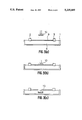
FIGS. 4 to 6 show a notional diagram of the above fundamental process. FIG. 4 shows an outline of the process using the underlying substrate A. Numeral 11 in FIG. 4(a) designates an organic thin film oriented in a particular direction in the film surface, and an arrow 12 is the orientation direction of the molecule. Numeral 14 in FIG. 4(b) designates a polymerizable molecular layer (second step). Numeral 15 in FIG. 4(c) designates a produced polymerized portion represented by hatching, and numeral 16 designates an unpolymerized portion (third step). FIG. 4(d) shows a state after removal of the unpolymerized portion (fourth step). In FIGS. 4(c) and 4(d), an arrow 17 is the orientation direction of molecules in the polymerized portion, i.e. the direction of the axis of polarization. In FIG. 4, the first step of producing the thin film oriented in a particular direction in the film surface at the gas/liquid interface is omitted. FIG. 5 shows the outline of the process using the underlying substrate B. An arrow 18 in FIG. 5(a) is the direction of rubbing applied to the substrate 10. FIG. 5(b) shows a state wherein the polymerizable molecular layer 14 has been produced (second step). FIG. 5(c) shows a state by hatching wherein the polymerized portion 15 has been produced (third step). FIG. 5(d) shows a state wherein the unpolymerized portion has been removed (fourth step). In FIGS. 5(c) and 5(d), an arrow 17 is the orientation direction of molecules in the polymerized portion, i.e. the direction of the axis of polarization.
FIG. 6 shows the outline of the process using the underlying substrate C. An arrow 19 in FIG. 6(a) is the direction of rubbing applied to the organic thin layer 20 on the substrate 10. FIG. 6(b) shows a state wherein the polymerizable molecular layer 14 has been produced (second step). FIG. 6(c) shows a state by hatching wherein the polymerized portion 15 has been produced (third step). FIG. 6(d) shows a state wherein the unpolymerized portion 16 has been removed (fourth step). In FIG. 6(c) and 6(d), an arrow 17 is the orientation direction of molecule in the the polymerized portion, i.e. the direction of the axis of polarization.
By using the process described above, a polarizer containing a portion having a polarizing ability and a portion having no polarizing ability in the same surface is obtained. Consequently, by repeating this process as many times as required, a polarizer containing in the same surface a plural number of portions which are different in polarizing ability therebetween or that containing in the same surface a plural number of portions which are different in the direction of polarization therebetween, can be produced.
FIG. 7 shows one typical embodiment of the process for producing a polarizer containing in the same surface a plural number of portions which are different in the direction of polarization therebetween. Explanation will be given below in the order of steps (a) to (h) in FIG. 7.
(a) The underlying substrate A is prepared for. That is, the organic thin film 11 wherein the molecules have been oriented in the direction of an arrow 12 is produced on the substrate 10 [FIG. 7(a)].
(b) The polymerizable molecular layer 14 is produced on the underlying substrate A [FIG. 7(b)].
(c) The polymerizable molecular layer 14 is polymerized into a desired pattern. The polymerized portion 15 is shown by hatching. An arrow 17 is the orientation direction of molecules in the polymerized portion 15, i.e. the direction of the axis of polarization. Numeral 16 designates the unpolymerized portion [FIG. 7(c)].
(d) The unpolymerized portion 16 is removed with a solvent [FIG. 7(d)].
(e) The organic thin film 11' is produced wherein the molecules have been oriented in the direction of an arrow 12' against the surface obtained by the above steps (a) to (d) [FIG. 7(e)].
(f) The polymerizable molecular layer 14' is produced on the organic thin film 11' [FIG. 7(f)].
(g) The polymerizable molecular layer 14' is polymerized into a desired pattern. The polymerized portion 15' is shown by hatching. An arrow 17' is the orientation direction of molecules in the polymerized portion 15', i.e. the direction of the axis of polarization. Numeral 16' designates the unpolymerized portion [FIG. 7(g)].
(h) The unpolymerized portion 16' is removed with a solvent [FIG. 7(h)].
In the embodiment shown in FIG. 7, the steps (a) to (d) and steps (e) to (h) are substantially the same. However, the latter half steps are carried out so that the orientation direction of molecules in the organic thin film 11' is a direction represented by an arrow 12'; the polymerized portion 15' is not positioned over the polymerized portion 15 produced in the former half steps; and the orientation direction of molecules, shown by an arrow 17', in the polymerized portion 15' is different from that, shown by an arrow 17, in the polymerized portion 15. Thus, as the sectional view of the completed polarizer in FIG. 7(h) shows, a polarizer containing the polymerized portions 15 and 15' of which the axes of polarization are perpendicular to each other, can be produced easily. FIG. 7 shows an example in which the polarization axes of two kinds of portion are perpendicular to each other. If the above method is used, however, the polarization axes of two kinds of portion can be determined so that they form an optional angle. Further, a polarizer containing in the same surface three or more kinds of portion which are different in the direction of polarization axis therebetween, also can be produced by repeating the above steps three times or more.
Further, a polarizer containing in the same surface a plural number of portions which are different in polarizing ability therebetween can also be produced by using a underlying organic thin film of different orientation degree for each polymerizable molecular layer or varying the kind of compound constituting the polymerizable molecular layer for each polymerizable molecular layer and repeating fundamentally the same steps as in FIG. 7.
In the foregoing embodiment, an organic oriented film was used to control the orientation of the polymerizable molecular layer, but the use of this organic oriented film can be replaced by the orientation technique of rubbing used to produce liquid crystal display devices.
All the steps described above are an embodiment for producing a polarizer on one surface alone of the substrate. However, it is also naturally possible as an application of the present invention to produce, on both surfaces of the substrate, the portions which are different in the direction of polarization or polarizing ability therebetween. One example is shown in FIG. 8. That is, the underlying organic thin films 11 and 11' controlling the orientation directions of the polymerized molecular layers are provided at both surfaces of the substrate 10 so that the orientation directions of molecules in both films are different from each other as shown by arrows 12 and 12', respectively, and further, the orientation directions of molecules in the polymerized portions 15 and 15' are made different from each other as shown by arrows 17 and 17', respectively.
Materials for the substrate used in the present invention include, in addition to glass and quartz, plastics such as polyethylene, polypropylene, polyacrylonitrile, polystyrene, polycarbonate, etc.
In the present invention, as examples of a compound which can be used as the film-forming molecule which enables the orientation of molecules to take a definite direction in the film surface by unidirectional or opposite bidirectional compression at the gas/liquid interface, compounds represented by the following formulae (1) to (15) can be given. ##STR1## wherein each of R1, R2, R3 and R4 represents a hydrogen atom or a structure represented by the formula, ##STR2## in which h is 2 to 18, k is 0 or 1, l is 1 to 18, m is 0 or 1 and p is 0 to 18, provided that at least one of R1, R2, R3 or R4 contained in the compounds has the structure represented by the above formula.
Among the compounds represented by the formulae (1) to (15), particularly preferred compounds are the following: ##STR3## wherein R5 represents a group represented by the formula, ##STR4## in which t is 2 to 15, ##STR5## wherein u is 3 to 21, and ##STR6## wherein v is 4 to 21.
In the present invention as an example of the compound usable as one constituting the polymerizable molecular layer, compounds represented by the formula (16) can be given:
Y.sub.1 --X.sub.1).sub.p (CH.sub.2).sub.q C.tbd.C--C.tbd.C--CH.sub.2).sub.r (X.sub.2).sub.s Y.sub.2                                   (16)
wherein each of p and s represents 0 or 1, each of q and r represents either one of integers of 1 to 15, each of X1 and X2 represents either one of --OSO2 --, --SO2 O--, --OCO--, --COO--, --CONH--, --NHCO--, --OCONH--, --NHCOO--, --CH2 O-- or --OCH2 --, and each of Y1 and Y2 represents either one of an alkyl group, phenyl group, alkylphenyl group, alkoxyphenyl group, halogenated phenyl group, nitrophenyl group, dinitrophenyl group, carbazolyl group, hydroxy group, carboxy group, anthryl group or alkyloxycarbonylalkyl group.
Among the compounds represented by the formula (16), examples of a particularly preferred compound include the following: ##STR7##
That the in-plane orientational order of molecules in the underlying film is given to the overlying layer, i.e. the polymerizable molecular layer after polymerization, is described in detail in a copending U.S. patent application Ser. No. 07/584971 already applied for by the present inventors.
The present invention will be illustrated more specifically with reference to the following example,s but the present invention is not to be interpreted as being limited thereto.
EXAMPLE 1
A 0.5 g/l chloroform solution of a polydiacetylene derivative represented by the formula (29) (hereinafter referred to as p-3BCMU), ##STR8## wherein R5 represents a substituent, ##STR9## was prepared, and this solution was added dropwise to the surface of pure water in the LB film-manufacturing apparatus shown in FIG. 1. After chloroform vaporized, the compressing barriers were slowly moved in two directions facing each other, as shown in FIG. 1, to compress the spread p-3BCMU film on the water surface. At the point when the surface pressure of the film reached 20 mN/m, the compressing barriers were stopped, and the in-plane orientational order of the p-3BCMU monomolecular film produced on the water surface was evaluated by measuring the polarization reflection spectrum. The measurement with polarized light was carried out by employing linearly polarized light vertically incident on the film on the water surface. As a result, it was found that the intensity of reflection was maximum and minimum when the direction of polarization was perpendicular (⊥) to the parallel (∥) to the compression direction, respectively. From this result, it became clear that the principal chain of the p-3BCMU molecules has been oriented perpendicular to the compression direction in the surface of the above monomolecular film. Also, it was found that, since this polarization characteristic does not show in-plane position dependency, the principal chain of the molecules has been oriented in the same direction and uniformly over the whole p-3BCMU monomolecular film (film area, about 60 cm2) formed on the water surface. Further, it was found that the dichroic ratio at about 620 nm of this film was about 20 from the above spectrum.
The oriented film of p-3BCMU thus produced on the water surface was transferred by only one layer to a transparent glass substrate previously subjected to hydrophobic treatment with hexamethyldisilazane, by the lifting method shown in FIG. 2. It was found that the transferred p-3BCMU film kept its orientational order even on the glass substrate.
Onto the organic thin film of p-3BCMU thus produced on the transparent glass substrate was deposited a diacetylene derivative represented by the formula (17) (hereinafter referred to as DCH) by the vacuum evaporation method. Thus, a polymerizable molecular layer of about 1000 Å in thickness comprising the diacetylene derivative monomer was obtained.
A photomask was applied to this polymerizable molecular layer and irradiated with ultraviolet rays from a mercury lamp to form a stripe-form polymerized pattern of 5 mm in width and 3 mm in interval on the film surface, as shown in FIGS. 9(a) and 9(b). FIG. 9(a) shows a plan view, and FIG. 9(b) shows a sectional view in which the shaded parts show the polymerized portion.
Next, this film was immersed in acetone together with the substrate to dissolve the unpolymerized monomer portion. Thus, a patterned film shown by the sectional view in FIG. 9(c) was obtained. The polarization absorption spectrum of the polymerized portion was measured to find that the direction of polarization maximizing the intensity of absorption resulting from the polymer main chain agreed with the orientation direction of molecules in the p-3BCMU monomolecular film used for the underlying organic thin film. In other words, it was found that the main chain of the DCH polymer produced by polymerization has been oriented in the same direction as that of the polymer main chain of the p-3BCMU monomolecular film which was the underlying organic thin film. The dichroic ratio of the polymerized portion obtained by the measurement of polarization absorption spectrum was about 5 at 650 nm, from which it was found that the polymerized portion had a polarizing ability.
From the results, it was found that a patterned polarizer containing a portion having a polarizing ability and a portion having no polarizing ability in the same surface can be produced by the method of the present invention. Coloration of the p-3BCMU monomolecular film used as the underlying organic thin film was extremely too slight to become a problem in practical use.
EXAMPLE 2
Onto the p-3BCMU monomolecular film produced as the underlying organic thin film on a glass substrate in the same manner as in Example 1 was vacuum-deposited each of diacetylene derivatives shown in Table 1 to produce a polymerizable molecular layer of about 1000 Å in thickness. Thereafter, the same polymerized pattern as in Example 1 was formed on each polymerizable molecular layer by the same process as in Example 1. The dichloric ratio of the polymerized portion obtained by the measurement of polarization absorption spectrum (at 550 nm) is shown in Table 1 for each diacetylene derivative used for deposition. In either case, the polymerized portion was found to be usable as the patterned polarizer.
              TABL,E 1                                                    
______________________________________                                    
                         Dichloric                                        
No.          Compound    ratio                                            
______________________________________                                    
1            Formula (18)                                                 
                         7                                                
2            Formula (19)                                                 
                         5                                                
3            Formula (20)                                                 
                         6                                                
4            Formula (21)                                                 
                         5                                                
5            Formula (22)                                                 
                         4                                                
6            Formula (23)                                                 
                         6                                                
7            Formula (24)                                                 
                         6                                                
8            Formula (25)                                                 
                         6                                                
9            Formula (26)                                                 
                         5                                                
10           Formula (27)                                                 
                         4                                                
11           Formula (28)                                                 
                         4                                                
______________________________________                                    
EXAMPLE 3
The oriented monomolecular film of a polydiacetylene derivative represented by the formula (30) (hereinafter referred to as p-4BCMU), ##STR10## wherein R6 represents a substituent, ##STR11## produced as the underlying organic thin film on a glass substrate in completely the same manner as in Example 1. Thereafter, onto the above oriented monomolecular film was deposited a polymerizable molecular layer of about 1000 Å in thickness comprising a diacetylene derivative represented by the formula (24) by the vacuum evaporation method. This polymerizable molecular layer was formed into the same polymerized pattern as in Example 1 by completely the same process as in Example 1. The dichloric ratio of the polymerized portion obtained by measurement of polarization absorption spectrum was about 4, from which it was found that the film of this Example can be used as the patterned polarizer.
EXAMPLE 4
A chloroform solution of a mixture of a polythiophene derivative represented by the formula (31) (hereinafter referred to as PHDT), ##STR12## and p-3BCMU in a 1:1 molar ratio prepared. The oriented monomolecular film of the was produced on the water surface in completely the same manner as in Example 1, and transferred to a glass substrate by the lifting method to obtain the underlying organic thin film. Onto this film was vacuum-deposited DCH to produce a polymerizable molecular layer of about 1000 Å in thickness. This polymerizable molecular layer was formed into the same polymerized pattern as in Example 1 by completely the same process as in Example 1. The dichroic ratio of the polymerized portion obtained by the measurement of polarization absorption spectrum was about 4, from which it was found that the film of this Example can be used as the patterned polarizer.
EXAMPLE 5
A chloroform solution of a mixture of polydihexylsilane represented by the formula (32), ##STR13## and p-3BCMU in a 1:1 molar ratio was prepared. The oriented monomolecular film of the mixture was produced on the water surface in completely the same manner as in Example 1, and transferred to a glass substrate by the lifting method to obtain the underlying organic thin film. Onto this film was vacuum-deposited DCH to produce a polymerizable molecular layer of about 1000 Å in thickness. This polymerizable molecular layer was formed into the same polymerized pattern as in Example 1 by completely the same process as in Example 1. The dichroic ratio of the polymerized portion obtained by the measurement of polarization absorption spectrum was 5, from which it was found that the film of this Example can be used as the patterned polarizer.
EXAMPLE 6
A 0.4 wt. % chlorophenol solution of polyethylene terephthalate was spinner-coated onto a glass substrate, and chlorophenol was volatilized by heating to produce an organic thin layer of polyethyleneterephthalate. The surface of this layer was repeatedly rubbed in one direction with silicone cloth to apply rubbing treatment thereto. Onto this layer was vacuum-deposited DCH to produce a polymerizable molecular layer of about 1000 Å in thickness. This polymerizable molecular layer was formed into the same polymerized pattern as in Example 1 by completely the same process as in Example 1. The dichroic ratio of the polymerized portion obtained by the measurement of polarization absorption spectrum was 10, from which it was found that the film of this Example can be used as the patterned polarizer.
EXAMPLE 7
4,4'-Diaminodiphenyl ether represented by the formula (33) and pyromellitic acid dianhydride represented by the formula (34) were polymerized in N-methyl-2-pyrrolidone to obtain a polyamide acid varnish: ##STR14##
This polyamide acid varnish was spinner-coated onto a glass substrate and baked at 300° C. to produce the organic thin layer of polyimide. The surface of this layer was repeatedly rubbed in one direction with silicone cloth to apply rubbing treatment thereto. Onto this layer was vacuum-deposited a diacetylene derivative represented by the formula (24) to produce the polymerizable molecular layer of about 1000 Å in thickness. This polymerizable molecular layer was formed into the same polymerized pattern as in Example 1 by the same process as in Example 1. The dichroic ratio of the polymerized portion obtained by the measurement of polarization absorption spectrum was 8, from which it was found that the film of this Example can be used as the patterned polarizer.
EXAMPLE 8
A 0.1 wt. % ethanol solution of a diacetylene compound represented by the formula (21) was applied by the casting method onto the oriented monomolecular film of p-3BCMU produced on a glass substrate in the same manner as in Example 1, and ethanol was volatilized. The polymerizable molecular layer thus obtained was formed into the same polymerized pattern as in Example 1 by the same process as in Example 1. The dichroic ratio of the polymerized portion obtained by the measurement of polarization absorption spectrum was 6, from which it was found that the film of this Example can be used as the patterned polarizer.
EXAMPLE 9
In the same manner as in Example 1, the oriented monomolecular film of p-3BCMU was produced as the underlying organic thin film on a glass substrate. Onto this oriented monomolecular film was deposited DCH by the vacuum evaporation method to produce the polymerizable molecular layer of about 700 Å in thickness. This layer was polymerized into the form of stripe of 3 mm in width and 3 mm in interval in the same manner as in Example 1, and the unpolymerized portion was removed with acetone [FIGS. 7(a) to 7(d)]. Onto the patterned polarizing film thus produced was once more deposited the oriented monomolecular film of p-3BCMU as the second organic thin film so that the orientation direction of the second thin film formed an angle of 90 degrees with that of the firstly produced organic thin film [FIG. 7(e)]. Onto this second thin film was further vacuum-deposited DCH to produce the polymerizable molecular layer of about 700 Å in thickness [FIG. 7(f)]. The polymerizable molecular layer thus produced was polymerized into the form of stripe of 3 mm in width and 3 mm in interval in the same manner as in Example 1. In this case, however, the second vacuum deposition of DCH was carried out so that the portion to be polymerized was not positioned over the polymerized portion firstly produced. The unpolymerized portion was removed to produce a polarizer having a section structure typically shown in FIG. 7(h). Thus, a polarizer was produced which comprised a plural number of portions arranged in the form of stripe, and in which the directions of polarization axis were different by an angle of 90 degrees between the adjacent portions.
Further, the same method as above was carried out using the substrate having the rubbing-treated organic thin layer shown in Example 6. As a result, the same polarizer as above containing portions which were different in the direction of polarization axis by 90 degrees therebetween, was obtained.
EXAMPLE 10
Such a patterned polarizer as shown in FIG. 10 was produced on a glass substrate with an ITO electrode pattern, using the same materials and method as in Example 1. In FIG. 10, the shaded portion shows a portion having a polarizing ability and the unshaded portion shows a portion having no polarizing ability. The size of one portion was made 500 microns in length and 500 microns in width. Onto this polarizer were deposited two molecular layers of the p-3BCMU monomolecular film so that the orientation direction of the monomolecular film agreed with the direction of polarization axis of the polarizer. One more piece of the same substrate was prepared. These two substrates were faced each other through a spacer of 8 μm so that their surfaces having the deposited film were turned inward and the direction of polarization axis of one polarizer formed an angle of 90 degrees with that of the other one. Thus, a liquid crystal device was obtained. A nematic liquid crystal marketed under the trade name of ZLI-1132 from Merk Co. was put into this liquid crystal device. It was found that the liquid crystal display device thus obtained showed a bright background and a good display quality as compared with the conventional liquid crystal display devices containing a twist-nematic liquid crystal.
Using two pieces polarizer prepared in each of Examples 1 to 9, liquid crystal display devices were produced in the same manner as above. As a result, every liquid crystal display device showed a bright and good display quality.

Claims (19)

What is claimed is:
1. A polarizer patterned with a plural number of portions having a polarizing ability or direction of polarization which comprises a substrate on which a surface oriented in a pre-determined direction has been produced, and a polymerized molecular layer which has been produced on the above surface and polymerized into a desired pattern and from which the unpolymerized portion has been removed.
2. A polarizer having a plural number of portions comprising a substrate on which a surface oriented in a pre-determined direction has been produced, a polymerized molecular layer which has been produced on the above surface and polymerized into a desired pattern and from which the unpolymerized portion has been removed, a surface which has been produced on the above polymerized molecular layer and oriented in a pre-determined direction and a polymerized molecular layer which has been produced on this surface and polymerized into a desired pattern and from which the unpolymerized portion has been removed, the above polymerized molecular layers being different in polarizing ability or direction of polarization.
3. A polarizer according to claim 1 or 2, wherein said oriented surface is produced by spreading organic molecules at a gas/liquid interface, compressing the spread molecules unidirectionally or in antiparallel directions to orient the molecules in a desired direction and then transferring the oriented organic molecules to the substrate.
4. A polarizer according to claim 1 or 2, wherein said oriented surface is produced by applying a rubbing treatment to the substrate.
5. A polarizer according to claim 2, wherein every polymerized molecular layer develops a color.
6. A polarizer according to claim 5, wherein the oriented surface is produced by spreading organic molecules at a gas/liquid interface, compressing the spread molecules unidirectionally or in antiparallel directions to orient the molecules in a desired direction and then transferring the oriented organic molecules to the substrate.
7. A polarizer according to claim 5, wherein the oriented surface is produced by applying a rubbing treatment in a desired direction.
8. A liquid crystal display device provided with a polarizer patterned with a plural number of portions having a polarizing ability or direction of polarization which comprises a first substrate on which a surface oriented in a pre-determined direction has been produced and a polymerized molecular layer which has been produced on the above surface and polymerized into a desired pattern and from which the unpolymerized portion has been removed, and a second substrate, the above polarizer and second substrate holding a liquid crystal therebetween, and a wiring for giving electric field to said liquid crystal being provided on each of the above polarizer and second substrate.
9. A liquid crystal display device provided with a polarizer having a plural number of portions comprising a first substrate on which a surface oriented in a predetermined direction has been produced, a polymerized molecular layer which has been produced on the above surface and polymerized into a desired pattern and from which the unpolymerized portion has been removed, a surface which has been produced on the above polymerized molecular layer and oriented in a pre-determined direction and a polymerized molecular layer which has been produced on this surface and polymerized into a desired pattern and from which the unpolymerized portion has been removed, the above polymerized molecular layers being different in polarizing ability or direction of polarization, and a second substrate, the above polarizer and second substrate holding a liquid crystal therebetween, and a wiring for giving electric field to said liquid crystal being provided on each of the above polarizer and second substrate.
10. A method for producing a polarizer patterned with a plural number of portions having a polarizing ability or direction of polarization comprising the first step of producing a surface oriented in a pre-determined direction on a substrate, the second step of producing a polymerizable molecular layer which comprises polymerizable molecules on the above surface, the third step of polymerizing the molecules in said polymerizable molecular layer into a desired pattern and the fourth step of removing the unpolymerized portion of said polymerizable molecular layer.
11. A method for producing a polarizer having in the same surface a plural number of portions which are different in polarizing ability or direction of polarization therebetween comprising the first step of producing a surface oriented in a pre-determined direction on a substrate, the second step of producing a polymerizable molecular layer which comprises polymerizable molecules on the above surface, the third step of polymerizing the molecules in said polymerizable molecular layer into a desired pattern, the fourth step of removing the unpolymerized portion of said polymerizable molecular layer, and the step of repeating the above first step to fourth step as many times as required with the orientation direction varied.
12. A method for producing a polarizer according to claim 10 or 11, wherein said first step is the step wherein organic molecules are spread at a gas/liquid interface and compressed unidirectionally or in antiparallel directions to orient the organic molecules in a desired direction, and the oriented organic molecules are transferred to a substrate.
13. A method for producing a polarizer according to claim 12, wherein the molecules in said polymerizable molecular layer comprise at least one diacetylene derivative.
14. A method for producing a polarizer according to claim 13, wherein said diacetylene derivative is at least one member selected from the group of: ##STR15##
15. A method for producing a polarizer according to claim 10 or 11, wherein said first step is the step of applying a rubbing treatment to the substrate.
16. A method for producing a polarizer according to claim 15, wherein the molecules in said polymerizable molecular layer comprise at least one diacetylene derivative.
17. A method for producing a polarizer according to claim 16, wherein said diacetylene derivative is at least one member selected from the group of: ##STR16##
18. A method for producing a polarizer according to one of claims 10 or 11, wherein the molecules in said polymerizable molecular layer comprise at least one diacetylene derivative.
19. A method for producing a polarizer according to claim 18, wherein said diacetylene derivative is at least one member selected from the group consisting of: ##STR17##
US07/662,642 1990-03-02 1991-03-01 Polarizer with patterned diacetylene layer, method for producing the same, and liquid crystal display device including such polarizer Expired - Lifetime US5235449A (en)

Priority Applications (1)

Application Number Priority Date Filing Date Title
US07/662,642 US5235449A (en) 1990-03-02 1991-03-01 Polarizer with patterned diacetylene layer, method for producing the same, and liquid crystal display device including such polarizer

Applications Claiming Priority (4)

Application Number Priority Date Filing Date Title
JP2049347A JPH03252606A (en) 1990-03-02 1990-03-02 Polarizing plate, production thereof and liquid crystal display element
JP2-049347 1990-03-02
US07/584,971 US5357357A (en) 1989-09-20 1990-09-19 Liquid crystal display devices with organic thin film formed by compressing molecules on liquid surface and transferring to substrate by horizontal lifting
US07/662,642 US5235449A (en) 1990-03-02 1991-03-01 Polarizer with patterned diacetylene layer, method for producing the same, and liquid crystal display device including such polarizer

Related Parent Applications (1)

Application Number Title Priority Date Filing Date
US07/584,971 Continuation-In-Part US5357357A (en) 1989-09-20 1990-09-19 Liquid crystal display devices with organic thin film formed by compressing molecules on liquid surface and transferring to substrate by horizontal lifting

Publications (1)

Publication Number Publication Date
US5235449A true US5235449A (en) 1993-08-10

Family

ID=27293611

Family Applications (1)

Application Number Title Priority Date Filing Date
US07/662,642 Expired - Lifetime US5235449A (en) 1990-03-02 1991-03-01 Polarizer with patterned diacetylene layer, method for producing the same, and liquid crystal display device including such polarizer

Country Status (1)

Country Link
US (1) US5235449A (en)

Cited By (52)

* Cited by examiner, † Cited by third party
Publication number Priority date Publication date Assignee Title
US5413657A (en) * 1992-06-03 1995-05-09 Nippon Oil Company, Limited Method of making compensator for liquid crystal display
US5512328A (en) * 1992-08-07 1996-04-30 Hitachi, Ltd. Method for forming a pattern and forming a thin film used in pattern formation
US5548427A (en) * 1994-01-21 1996-08-20 Sharp Kabushiki Kaisha Switchable holographic apparatus
EP0770889A2 (en) * 1995-10-13 1997-05-02 Sharp Kabushiki Kaisha Optical element, method of making an optical element, and 3D display
US5686975A (en) * 1993-10-18 1997-11-11 Stereographics Corporation Polarel panel for stereoscopic displays
DE19621512A1 (en) * 1996-05-29 1997-12-04 Univ Schiller Jena Polarisation establishment with respect to wavelength of source spectra
EP0829744A2 (en) * 1996-09-12 1998-03-18 Sharp Kabushiki Kaisha Parallax barrier and display passive polarisation modulating optical element & method of making such an element
US5739952A (en) * 1994-04-14 1998-04-14 Kabushiki Kaisha Sankyo Seiki Seisakusho Polarizing beam splitter and optical head assembly
US5751389A (en) * 1994-09-08 1998-05-12 Sumitomo Chemical Company Film containing oriented dye, method of manufacturing the same, and polarizer and liquid crystal display unit utilizing the same
US5805250A (en) * 1995-10-31 1998-09-08 Sharp Kabushiki Kaisha Liquid crystal display device with contact holes extending through interlayer insulating film between switching elements and pixel electrodes
US6061043A (en) * 1996-02-20 2000-05-09 Sharp Kabushiki Kaisha Liquid crystal display having grey levels with reduced variations due to temperature and liquid crystal variations
US6108131A (en) * 1998-05-14 2000-08-22 Moxtek Polarizer apparatus for producing a generally polarized beam of light
US6122103A (en) * 1999-06-22 2000-09-19 Moxtech Broadband wire grid polarizer for the visible spectrum
US6171762B1 (en) 1996-03-28 2001-01-09 Corning Incorporated Polarizing glasses having integral non-polarizing regions
US6188451B1 (en) * 1996-07-04 2001-02-13 Sharp Kabushiki Kaisha Optical rotary device and manufacturing method thereof and image display device using thereof
US6208463B1 (en) 1998-05-14 2001-03-27 Moxtek Polarizer apparatus for producing a generally polarized beam of light
US6234634B1 (en) 1999-07-28 2001-05-22 Moxtek Image projection system with a polarizing beam splitter
US6243199B1 (en) 1999-09-07 2001-06-05 Moxtek Broad band wire grid polarizing beam splitter for use in the visible wavelength region
US6288840B1 (en) 1999-06-22 2001-09-11 Moxtek Imbedded wire grid polarizer for the visible spectrum
US6447120B2 (en) 1999-07-28 2002-09-10 Moxtex Image projection system with a polarizing beam splitter
US20030017856A1 (en) * 2001-06-20 2003-01-23 3M Innovative Properties Company Method for altering the appearance of liquid crystal displays using exchangable front polarizers
US6524773B1 (en) 1996-03-28 2003-02-25 Corning Incorporated Polarizing glasses having integral non-polarizing regions
US6538714B1 (en) 1999-10-25 2003-03-25 3M Innovative Properties Company Dual color guest-host polarizers and devices containing guest-host polarizers
US6574044B1 (en) 1999-10-25 2003-06-03 3M Innovative Properties Company Polarizer constructions and display devices exhibiting unique color effects
US6642977B2 (en) 2001-06-20 2003-11-04 3M Innovative Properties Company Liquid crystal displays with repositionable front polarizers
US6666556B2 (en) 1999-07-28 2003-12-23 Moxtek, Inc Image projection system with a polarizing beam splitter
US6686980B1 (en) * 1999-11-04 2004-02-03 Fuji Photo Film Co., Ltd. Anisotropic film containing a copolymer including a monomer containing a dichroic dye and liquid crystal display containing the antisotropic film
US20040125449A1 (en) * 2002-12-30 2004-07-01 Sales Tasso R. Grid polarizer with suppressed reflectivity
US6785050B2 (en) 2002-05-09 2004-08-31 Moxtek, Inc. Corrosion resistant wire-grid polarizer and method of fabrication
US20050073065A1 (en) * 2002-04-06 2005-04-07 Mack Jon M. Process for making an intrinsic polarizer
US20060119937A1 (en) * 2004-12-06 2006-06-08 Moxtek, Inc. Multilayer wire-grid polarizer
US7184115B2 (en) 2002-01-07 2007-02-27 Moxtek, Inc. Display apparatus with two polarization compensators
US7221420B2 (en) 2002-01-07 2007-05-22 Sony Corporation Display with a wire grid polarizing beamsplitter
US7306338B2 (en) 1999-07-28 2007-12-11 Moxtek, Inc Image projection system with a polarizing beam splitter
KR100804849B1 (en) * 2001-10-16 2008-02-20 다이니폰 인사츠 가부시키가이샤 Method of producing optical element by patterning of liquid crystal films
US7375887B2 (en) 2001-03-27 2008-05-20 Moxtek, Inc. Method and apparatus for correcting a visible light beam using a wire-grid polarizer
CN100410776C (en) * 2004-06-30 2008-08-13 乐金显示有限公司 Liquid crystal display device and method for fabricating the same
US20090219465A1 (en) * 2008-02-29 2009-09-03 Infinite Z, Inc. Polarizing Display Device
US7630133B2 (en) 2004-12-06 2009-12-08 Moxtek, Inc. Inorganic, dielectric, grid polarizer and non-zero order diffraction grating
US7789515B2 (en) 2007-05-17 2010-09-07 Moxtek, Inc. Projection device with a folded optical path and wire-grid polarizer
US7800823B2 (en) 2004-12-06 2010-09-21 Moxtek, Inc. Polarization device to polarize and further control light
US20100328768A1 (en) * 2009-06-25 2010-12-30 Michael Lines Nano fractal diffuser
US7961393B2 (en) 2004-12-06 2011-06-14 Moxtek, Inc. Selectively absorptive wire-grid polarizer
US8467128B2 (en) 2008-11-19 2013-06-18 Shanghai Lexvu Opto Microelectronics Technology Co., Ltd. Polarizing cube and method of fabricating the same
US8611007B2 (en) 2010-09-21 2013-12-17 Moxtek, Inc. Fine pitch wire grid polarizer
US8755113B2 (en) 2006-08-31 2014-06-17 Moxtek, Inc. Durable, inorganic, absorptive, ultra-violet, grid polarizer
US8796704B2 (en) 2011-05-02 2014-08-05 Innolux Corporation Emissive display having polarizer and retarder films
US8873144B2 (en) 2011-05-17 2014-10-28 Moxtek, Inc. Wire grid polarizer with multiple functionality sections
US8913320B2 (en) 2011-05-17 2014-12-16 Moxtek, Inc. Wire grid polarizer with bordered sections
US8913321B2 (en) 2010-09-21 2014-12-16 Moxtek, Inc. Fine pitch grid polarizer
US8922890B2 (en) 2012-03-21 2014-12-30 Moxtek, Inc. Polarizer edge rib modification
US9348076B2 (en) 2013-10-24 2016-05-24 Moxtek, Inc. Polarizer with variable inter-wire distance

Citations (12)

* Cited by examiner, † Cited by third party
Publication number Priority date Publication date Assignee Title
JPS5376049A (en) * 1976-12-17 1978-07-06 Hitachi Ltd Affixing method of polariizing plates of varying characteristics
JPS5831318A (en) * 1981-08-19 1983-02-24 Nec Corp Liquid crystal display device and its manufacture
JPS58120220A (en) * 1982-01-11 1983-07-18 Nitto Electric Ind Co Ltd Polarizing plate for simultaneous display of negative and positive
JPS5958419A (en) * 1982-09-28 1984-04-04 Nitto Electric Ind Co Ltd Polarizer
JPS60216337A (en) * 1984-04-12 1985-10-29 Canon Inc Digital parallel optical arithmetic device
JPS60222824A (en) * 1984-04-20 1985-11-07 Matsushita Electric Ind Co Ltd Liquid crystal display device
JPS6159428A (en) * 1984-08-31 1986-03-26 Fujitsu Ltd Liquid crystal display element
JPS61278827A (en) * 1985-06-04 1986-12-09 Sharp Corp Liquid crystal display element
JPS63201626A (en) * 1987-02-18 1988-08-19 Nec Home Electronics Ltd Liquid crystal stereoscopic image device
US4863763A (en) * 1987-07-13 1989-09-05 Mitsubishi Petrochemical Co., Ltd. Process for producing molecular orientated film
US5007715A (en) * 1988-03-10 1991-04-16 U.S. Philips Corporation Display and pick-up device for stereoscopic picture display
US5122890A (en) * 1987-11-06 1992-06-16 Makow David M Electro-optic animated displays and indicators employing electro-optical cells and mosaic segment polarizer

Patent Citations (12)

* Cited by examiner, † Cited by third party
Publication number Priority date Publication date Assignee Title
JPS5376049A (en) * 1976-12-17 1978-07-06 Hitachi Ltd Affixing method of polariizing plates of varying characteristics
JPS5831318A (en) * 1981-08-19 1983-02-24 Nec Corp Liquid crystal display device and its manufacture
JPS58120220A (en) * 1982-01-11 1983-07-18 Nitto Electric Ind Co Ltd Polarizing plate for simultaneous display of negative and positive
JPS5958419A (en) * 1982-09-28 1984-04-04 Nitto Electric Ind Co Ltd Polarizer
JPS60216337A (en) * 1984-04-12 1985-10-29 Canon Inc Digital parallel optical arithmetic device
JPS60222824A (en) * 1984-04-20 1985-11-07 Matsushita Electric Ind Co Ltd Liquid crystal display device
JPS6159428A (en) * 1984-08-31 1986-03-26 Fujitsu Ltd Liquid crystal display element
JPS61278827A (en) * 1985-06-04 1986-12-09 Sharp Corp Liquid crystal display element
JPS63201626A (en) * 1987-02-18 1988-08-19 Nec Home Electronics Ltd Liquid crystal stereoscopic image device
US4863763A (en) * 1987-07-13 1989-09-05 Mitsubishi Petrochemical Co., Ltd. Process for producing molecular orientated film
US5122890A (en) * 1987-11-06 1992-06-16 Makow David M Electro-optic animated displays and indicators employing electro-optical cells and mosaic segment polarizer
US5007715A (en) * 1988-03-10 1991-04-16 U.S. Philips Corporation Display and pick-up device for stereoscopic picture display

Non-Patent Citations (12)

* Cited by examiner, † Cited by third party
Title
D. Lupo et al, "Structure and properties of Langmuir-Blodgett films made from polyamides," Thin Solid Films, vol. 178, No. 1, Nov. 11, 1989, Netherlands, pp. 403-411.
D. Lupo et al, Structure and properties of Langmuir Blodgett films made from polyamides, Thin Solid Films, vol. 178, No. 1, Nov. 11, 1989, Netherlands, pp. 403 411. *
D. Nerger et al, "Polyesters and Polyurethanes as prepolymerized materials for Langmuir-Blodgett films: preparation and characterization of multilayers," Thin Solid Films, vol. 178, No. 1, Nov. 1, 1989, Netherlands, pp. 253-259.
D. Nerger et al, Polyesters and Polyurethanes as prepolymerized materials for Langmuir Blodgett films: preparation and characterization of multilayers, Thin Solid Films, vol. 178, No. 1, Nov. 1, 1989, Netherlands, pp. 253 259. *
I. Watanabe et al, "Fabrication of novel electrically conductive Langmuir-Blodgett thin films of the poly(3-alkyl-thiophenes)," Thin Solid Films, vol. 179, No. 1, Nov. 11, 1989, Netherlands, pp. 199-206.
I. Watanabe et al, Fabrication of novel electrically conductive Langmuir Blodgett thin films of the poly(3 alkyl thiophenes), Thin Solid Films, vol. 179, No. 1, Nov. 11, 1989, Netherlands, pp. 199 206. *
J. Nehring et al, "High-pretilt polyphenylene layers for liquid-crystal displays", Applied Physics Letters, vol. 51, No. 16, Oct. 19, 1987, New York, US, pp. 1283-1284.
J. Nehring et al, High pretilt polyphenylene layers for liquid crystal displays , Applied Physics Letters, vol. 51, No. 16, Oct. 19, 1987, New York, US, pp. 1283 1284. *
M. Sugi, "Langmuir-Blodgett films--a course towards molecular electronics: a review," Journal of Molecular Electronics, vol. 1, 1985, Chichester, GB, pp. 3-17.
M. Sugi, Langmuir Blodgett films a course towards molecular electronics: a review, Journal of Molecular Electronics, vol. 1, 1985, Chichester, GB, pp. 3 17. *
Y. Nishikata et al, "Preparation and properties of poly (p-phenylene) Langmuir-Blodgett film", Thin Solid Films, vol. 179, No. 1, Nov. 11, 1989, Netherlands, pp. 191-197.
Y. Nishikata et al, Preparation and properties of poly (p phenylene) Langmuir Blodgett film , Thin Solid Films, vol. 179, No. 1, Nov. 11, 1989, Netherlands, pp. 191 197. *

Cited By (73)

* Cited by examiner, † Cited by third party
Publication number Priority date Publication date Assignee Title
US5413657A (en) * 1992-06-03 1995-05-09 Nippon Oil Company, Limited Method of making compensator for liquid crystal display
US5512328A (en) * 1992-08-07 1996-04-30 Hitachi, Ltd. Method for forming a pattern and forming a thin film used in pattern formation
US5686975A (en) * 1993-10-18 1997-11-11 Stereographics Corporation Polarel panel for stereoscopic displays
US5548427A (en) * 1994-01-21 1996-08-20 Sharp Kabushiki Kaisha Switchable holographic apparatus
US5739952A (en) * 1994-04-14 1998-04-14 Kabushiki Kaisha Sankyo Seiki Seisakusho Polarizing beam splitter and optical head assembly
US5751389A (en) * 1994-09-08 1998-05-12 Sumitomo Chemical Company Film containing oriented dye, method of manufacturing the same, and polarizer and liquid crystal display unit utilizing the same
EP0770889A2 (en) * 1995-10-13 1997-05-02 Sharp Kabushiki Kaisha Optical element, method of making an optical element, and 3D display
US5861931A (en) * 1995-10-13 1999-01-19 Sharp Kabushiki Kaisha Patterned polarization-rotating optical element and method of making the same, and 3D display
EP0770889A3 (en) * 1995-10-13 1998-05-20 Sharp Kabushiki Kaisha Optical element, method of making an optical element, and 3D display
US5805250A (en) * 1995-10-31 1998-09-08 Sharp Kabushiki Kaisha Liquid crystal display device with contact holes extending through interlayer insulating film between switching elements and pixel electrodes
US6061043A (en) * 1996-02-20 2000-05-09 Sharp Kabushiki Kaisha Liquid crystal display having grey levels with reduced variations due to temperature and liquid crystal variations
US6524773B1 (en) 1996-03-28 2003-02-25 Corning Incorporated Polarizing glasses having integral non-polarizing regions
US6171762B1 (en) 1996-03-28 2001-01-09 Corning Incorporated Polarizing glasses having integral non-polarizing regions
DE19621512A1 (en) * 1996-05-29 1997-12-04 Univ Schiller Jena Polarisation establishment with respect to wavelength of source spectra
US6188451B1 (en) * 1996-07-04 2001-02-13 Sharp Kabushiki Kaisha Optical rotary device and manufacturing method thereof and image display device using thereof
US6437915B2 (en) 1996-09-12 2002-08-20 Sharp Kabushiki Kaisha Parallax barrier, display, passive polarization modulating optical element and method of making such an element
EP0829744A3 (en) * 1996-09-12 1999-02-03 Sharp Kabushiki Kaisha Parallax barrier and display passive polarisation modulating optical element & method of making such an element
US6046849A (en) * 1996-09-12 2000-04-04 Sharp Kabushiki Kaisha Parallax barrier, display, passive polarisation modulating optical element and method of making such an element
EP0829744A2 (en) * 1996-09-12 1998-03-18 Sharp Kabushiki Kaisha Parallax barrier and display passive polarisation modulating optical element & method of making such an element
US6108131A (en) * 1998-05-14 2000-08-22 Moxtek Polarizer apparatus for producing a generally polarized beam of light
US6208463B1 (en) 1998-05-14 2001-03-27 Moxtek Polarizer apparatus for producing a generally polarized beam of light
US6452724B1 (en) 1998-05-14 2002-09-17 Moxtek Polarizer apparatus for producing a generally polarized beam of light
US6710921B2 (en) 1998-05-14 2004-03-23 Moxtek Polarizer apparatus for producing a generally polarized beam of light
US6288840B1 (en) 1999-06-22 2001-09-11 Moxtek Imbedded wire grid polarizer for the visible spectrum
US6122103A (en) * 1999-06-22 2000-09-19 Moxtech Broadband wire grid polarizer for the visible spectrum
US6234634B1 (en) 1999-07-28 2001-05-22 Moxtek Image projection system with a polarizing beam splitter
US6447120B2 (en) 1999-07-28 2002-09-10 Moxtex Image projection system with a polarizing beam splitter
US7306338B2 (en) 1999-07-28 2007-12-11 Moxtek, Inc Image projection system with a polarizing beam splitter
US6666556B2 (en) 1999-07-28 2003-12-23 Moxtek, Inc Image projection system with a polarizing beam splitter
US6243199B1 (en) 1999-09-07 2001-06-05 Moxtek Broad band wire grid polarizing beam splitter for use in the visible wavelength region
US6730446B2 (en) 1999-10-25 2004-05-04 3M Innovative Properties Company Dual color guest-host polarizers and devices containing guest-host polarizers
US20030147043A1 (en) * 1999-10-25 2003-08-07 3M Innovative Properties Company Dual color guest-host polarizers and devices containing guest-host polarizers
US6574044B1 (en) 1999-10-25 2003-06-03 3M Innovative Properties Company Polarizer constructions and display devices exhibiting unique color effects
US6538714B1 (en) 1999-10-25 2003-03-25 3M Innovative Properties Company Dual color guest-host polarizers and devices containing guest-host polarizers
US20030184862A1 (en) * 1999-10-25 2003-10-02 3M Innovative Properties Company Polarizer constructions and display devices exhibiting unique color effects
US6768586B2 (en) 1999-10-25 2004-07-27 3M Innovative Properties Company Polarizer constructions and display devices exhibiting unique color effects
US20040246580A1 (en) * 1999-10-25 2004-12-09 3M Innovative Properties Company Polarizer constructions and display devices exhibiting unique color effects
US6686980B1 (en) * 1999-11-04 2004-02-03 Fuji Photo Film Co., Ltd. Anisotropic film containing a copolymer including a monomer containing a dichroic dye and liquid crystal display containing the antisotropic film
US7375887B2 (en) 2001-03-27 2008-05-20 Moxtek, Inc. Method and apparatus for correcting a visible light beam using a wire-grid polarizer
US20030017856A1 (en) * 2001-06-20 2003-01-23 3M Innovative Properties Company Method for altering the appearance of liquid crystal displays using exchangable front polarizers
US6642977B2 (en) 2001-06-20 2003-11-04 3M Innovative Properties Company Liquid crystal displays with repositionable front polarizers
KR100804849B1 (en) * 2001-10-16 2008-02-20 다이니폰 인사츠 가부시키가이샤 Method of producing optical element by patterning of liquid crystal films
US7221420B2 (en) 2002-01-07 2007-05-22 Sony Corporation Display with a wire grid polarizing beamsplitter
US7184115B2 (en) 2002-01-07 2007-02-27 Moxtek, Inc. Display apparatus with two polarization compensators
US20050073065A1 (en) * 2002-04-06 2005-04-07 Mack Jon M. Process for making an intrinsic polarizer
US6785050B2 (en) 2002-05-09 2004-08-31 Moxtek, Inc. Corrosion resistant wire-grid polarizer and method of fabrication
US20040125449A1 (en) * 2002-12-30 2004-07-01 Sales Tasso R. Grid polarizer with suppressed reflectivity
US7113335B2 (en) 2002-12-30 2006-09-26 Sales Tasso R Grid polarizer with suppressed reflectivity
CN100410776C (en) * 2004-06-30 2008-08-13 乐金显示有限公司 Liquid crystal display device and method for fabricating the same
US20060119937A1 (en) * 2004-12-06 2006-06-08 Moxtek, Inc. Multilayer wire-grid polarizer
US7570424B2 (en) 2004-12-06 2009-08-04 Moxtek, Inc. Multilayer wire-grid polarizer
US7630133B2 (en) 2004-12-06 2009-12-08 Moxtek, Inc. Inorganic, dielectric, grid polarizer and non-zero order diffraction grating
US7800823B2 (en) 2004-12-06 2010-09-21 Moxtek, Inc. Polarization device to polarize and further control light
US7813039B2 (en) 2004-12-06 2010-10-12 Moxtek, Inc. Multilayer wire-grid polarizer with off-set wire-grid and dielectric grid
US7961393B2 (en) 2004-12-06 2011-06-14 Moxtek, Inc. Selectively absorptive wire-grid polarizer
US8027087B2 (en) 2004-12-06 2011-09-27 Moxtek, Inc. Multilayer wire-grid polarizer with off-set wire-grid and dielectric grid
US8755113B2 (en) 2006-08-31 2014-06-17 Moxtek, Inc. Durable, inorganic, absorptive, ultra-violet, grid polarizer
US8947772B2 (en) 2006-08-31 2015-02-03 Moxtek, Inc. Durable, inorganic, absorptive, ultra-violet, grid polarizer
US7789515B2 (en) 2007-05-17 2010-09-07 Moxtek, Inc. Projection device with a folded optical path and wire-grid polarizer
US20090219465A1 (en) * 2008-02-29 2009-09-03 Infinite Z, Inc. Polarizing Display Device
US8467128B2 (en) 2008-11-19 2013-06-18 Shanghai Lexvu Opto Microelectronics Technology Co., Ltd. Polarizing cube and method of fabricating the same
US8248696B2 (en) 2009-06-25 2012-08-21 Moxtek, Inc. Nano fractal diffuser
US20100328768A1 (en) * 2009-06-25 2010-12-30 Michael Lines Nano fractal diffuser
US8913321B2 (en) 2010-09-21 2014-12-16 Moxtek, Inc. Fine pitch grid polarizer
US8611007B2 (en) 2010-09-21 2013-12-17 Moxtek, Inc. Fine pitch wire grid polarizer
US9523805B2 (en) 2010-09-21 2016-12-20 Moxtek, Inc. Fine pitch wire grid polarizer
US8796704B2 (en) 2011-05-02 2014-08-05 Innolux Corporation Emissive display having polarizer and retarder films
US8913320B2 (en) 2011-05-17 2014-12-16 Moxtek, Inc. Wire grid polarizer with bordered sections
US8873144B2 (en) 2011-05-17 2014-10-28 Moxtek, Inc. Wire grid polarizer with multiple functionality sections
US8922890B2 (en) 2012-03-21 2014-12-30 Moxtek, Inc. Polarizer edge rib modification
US9348076B2 (en) 2013-10-24 2016-05-24 Moxtek, Inc. Polarizer with variable inter-wire distance
US9354374B2 (en) 2013-10-24 2016-05-31 Moxtek, Inc. Polarizer with wire pair over rib
US9632223B2 (en) 2013-10-24 2017-04-25 Moxtek, Inc. Wire grid polarizer with side region

Similar Documents

Publication Publication Date Title
US5235449A (en) Polarizer with patterned diacetylene layer, method for producing the same, and liquid crystal display device including such polarizer
KR100327764B1 (en) Polarizing element, polarizing plate and manufacturing method
EP0777865B1 (en) Film containing oriented dye, method of manufacturing the same, and polarizer and liquid crystal display unit utilizing the same
US7381507B2 (en) Photo-patterned light polarizing films
Ichimura et al. Surface-assisted photolithography to form anisotropic dye layers as a new horizon of command surfaces
US20060232860A1 (en) Photo-induced dichroic polarizers and fabrication methods thereof
US8576485B2 (en) Photo-induced dichroic polarizers and fabrication methods thereof
EP0444703B1 (en) Polarizers, a method for producing the same and liquid crystal display devices
EP0418833A2 (en) Organic thin film and liquid crystal display devices with the same
US6404472B1 (en) Film containing oriented dye, method of manufacturing the same, and polarizer and liquid crystal display unit utilizing the same
JPH07261024A (en) Polarizing element, polarizing plate and production of these
US3623794A (en) Spectral zonal encoder
GB2324881A (en) Patterned optical elements
US6133973A (en) Film containing oriented dye, method of manufacturing the same, and polarizer and liquid crystal display unit utilizing the same
JP3065154B2 (en) Color filter, method of manufacturing the same, and display device and pickup device provided with the color filter
KR0166886B1 (en) Photopolymer using polyimide fluoro cinnamate and liquid crystal aligning film using same
JPH01130102A (en) Method for dyeing coating film
JPH0973015A (en) Oriented dye-containing film, its production, polarizing element and liquid crystal display device
JPH0148524B2 (en)
JPH09281335A (en) Production of oriented dye film
KR890001077B1 (en) Color filter with multilayer and the method of manufacturing it
KR100294683B1 (en) Method for forming alignment film of liquid crystal display
JPH02139522A (en) Liquid crystal display device and production thereof
JP2000111967A (en) Associated pigment thin film, its manufacture and optical switch
Kozenkov et al. 47.3: Thin Photo‐Patterned Internal Polarizers for LCDs

Legal Events

Date Code Title Description
AS Assignment

Owner name: HITACHI, LTD., 6, KANDA SURUGADAI 4-CHOME, CHIYODA

Free format text: ASSIGNMENT OF ASSIGNORS INTEREST.;ASSIGNORS:IMAZEKI, SHUJI;TOMIOKA, YASUSHI;TANAKA, NAOKI;AND OTHERS;REEL/FRAME:005631/0333

Effective date: 19910220

STCF Information on status: patent grant

Free format text: PATENTED CASE

FEPP Fee payment procedure

Free format text: PAYOR NUMBER ASSIGNED (ORIGINAL EVENT CODE: ASPN); ENTITY STATUS OF PATENT OWNER: LARGE ENTITY

FPAY Fee payment

Year of fee payment: 4

FPAY Fee payment

Year of fee payment: 8

FPAY Fee payment

Year of fee payment: 12