US5223448A - Method for producing a layered capacitor structure for a dynamic random access memory device - Google Patents
Method for producing a layered capacitor structure for a dynamic random access memory device Download PDFInfo
- Publication number
- US5223448A US5223448A US07/732,165 US73216591A US5223448A US 5223448 A US5223448 A US 5223448A US 73216591 A US73216591 A US 73216591A US 5223448 A US5223448 A US 5223448A
- Authority
- US
- United States
- Prior art keywords
- polysilicon layer
- layer
- over
- portions
- polysilicon
- Prior art date
- Legal status (The legal status is an assumption and is not a legal conclusion. Google has not performed a legal analysis and makes no representation as to the accuracy of the status listed.)
- Expired - Lifetime
Links
Images


Classifications
-
- H—ELECTRICITY
- H01—ELECTRIC ELEMENTS
- H01L—SEMICONDUCTOR DEVICES NOT COVERED BY CLASS H10
- H01L28/00—Passive two-terminal components without a potential-jump or surface barrier for integrated circuits; Details thereof; Multistep manufacturing processes therefor
- H01L28/40—Capacitors
-
- H—ELECTRICITY
- H10—SEMICONDUCTOR DEVICES; ELECTRIC SOLID-STATE DEVICES NOT OTHERWISE PROVIDED FOR
- H10B—ELECTRONIC MEMORY DEVICES
- H10B12/00—Dynamic random access memory [DRAM] devices
- H10B12/01—Manufacture or treatment
- H10B12/02—Manufacture or treatment for one transistor one-capacitor [1T-1C] memory cells
- H10B12/03—Making the capacitor or connections thereto
- H10B12/033—Making the capacitor or connections thereto the capacitor extending over the transistor
Definitions
- the present invention relates generally to dynamic random access memory devices, and more specifically to improvements in producing a layered capacitor structure for a random access memory cell.
- a memory cell used in a dynamic random access memory device is composed of a memory cell capacitor, such as a stacked capacitor, and a transfer transistor.
- a memory cell capacitor such as a stacked capacitor
- a transfer transistor In order to reduce the cost, and increase the speed of operation, the memory devices have become increasingly more miniaturized. In order to achieve this, each memory cell must occupy less space on the device. However, the cell capacitor must have roughly the same capacitance. The capacitance of a capacitor is proportional to the area of the electrodes. Thus, in order to maintain the capacitance level as the allotted area on the device becomes smaller, various new types of capacitors have been introduced, such as trench capacitors, stacked capacitors and similar devices.
- U.S. Pat. No. 4,910,566 discloses an improved cell capacitor for a DRAM cell.
- the patent discloses a memory cell capacitor consisting of a plate shaped film and a vertical projection film which are formed of doped polysilicon.
- the plate-shaped film and vertical projection film are formed on an interlayer insulation film.
- the vertical projection film is in contact with a sidewall of the plate-shaped film. With the vertical projection film, it is possible to increase the capacitance of the memory cell capacitance.
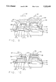
- FIGS. 1 and 2 depict the general nature of the capacitor known in the prior art.
- a transfer transistor is shown consisting of a source 10 and drain 12, and a gate electrode 14.
- An insulating film 16 extends over the gate electrode.
- the transistor is shown a thick field oxide 18, and a gate electrode 20 of an adjacent memory cell, with an overlying insulating film 16.
- the cell capacitor Positioned between the electrodes 14 and 20 is the cell capacitor consisting of a polysilicon layer formed of a horizontal plate portion 22 joined to a vertical projection portion 24.
- a thin insulation layer 26 overlays the cell capacitor.
- the cell capacitor of U.S. Pat. No. 4,910,566 suffers from very serious shortcomings in that fabrication, as described, requires a very precise mask adjustment to form the opening over the drain region. Particularly for deep submicron technology, the tight control requirement of this patent will be more critical in order to keep the proper alignment. Also the concentrations of the dopant in the vertical projection portions 24 is low due to the limitation of ion implantation.
- a more specific object of the invention is to provide a new method to provide a polysilicon layer structure of a cell capacitor for a DRAM device, which requires a minimum of photo-lithographic masking steps, and also provides a more uniform dopant concentration in the polysilicon layer.
- a further object of this invention is the achievement of an overhead FIN structure to increase the capacitance by using a silicon oxide instead of the first polysilicon layer and etching of the silicon oxide.
- the polysilicon spacer enhances the stability of the FIN and word line, as dopant source at the vertical sidewall.
- the above objects of the present invention can be achieved by forming a first polysilicon layer over at least the surface of drain region, the gate electrode of the transfer transistor, and the adjacent field oxide, forming an opening in the first polysilicon layer over the drain region, depositing a second doped polysilicon layer, forming an insulating layer over the second polysilicon layer, exposing the device to a reactive ion etch to remove the insulating layer on the horizontal surface, but leaving portions on vertical and sharply inclined surfaces, removing the portions of the second polysilicon layer not masked by the insulating layer, removing the insulating layer, opening the window to the drain region, depositing a third polysilicon layer and ion implanting a dopant therein, and removing the portions of the first and third polysilicon layers not required for the capacitor.
- FIG. 1 is a top plan view of a cell capacitor known to the prior art.
- FIG. 2 is an elevational view in cross section taken on line 2--2 of FIG. 1.
- FIGS. 3, 4, 5, 6A, 7, 8 and 9 are a sequence of cross sectional views that depict the process steps of the first embodiment method of the inventions.
- FIG. 6b is a cross sectional view taken on line 6b-6b in FIG. 6a.
- FIG. 10 is a schematic cross-sectional view of the final device structure after passivation and metallurgy has been formed over the device structures for a second embodiment.
- FIG. 3 there is shown a partially completed DRAM cell having a transistor, having a source region 10, a drain region 12, a gate oxide 13, and a gate electrode 14. As shown the drain region abuts a thick field oxide region 18. An insulation film 16 is shown covering the surface of the device, including a gate electrode 20 for an adjacent cell that overlays field oxide 18.
- the described cell structure is conventional.
- lightly doped regions 15 are provided adjacent to the source and drain regions 10 and 12, respectifully, as is well known in the art.
- a first polysilicon layer 30 is deposited on the top surface of the device, using conventional techniques.
- the thickness of layer 30 will depend on the scale of the device structure, but in general is in the range of about 100 to 500 nanometers.
- an opening 32 is formed over region 12, using conventional photolithographic and masking techniques.
- the opening 32 is formed by a commercially available plasma dry etcher with significantly high polysilicon to silicon oxide selectivity and preferably higher than 20 to 1.
- a second doped polysilicon layer 34 is deposited over layer 30, and over exposed insulation film 16, over drain region 12.
- the thickness of layer 34 is preferably in the range of about 100 to 400 nanometers.
- the dopant preferably is phosphorus in situ doped with a concentration in the range of about 1 ⁇ 10 20 to 8 ⁇ 10 20 atoms/cm 3 .
- the dopant in layer 34 is combined in the reactants that are used to deposit the polysilicon material, as is well known.
- insulation layer 36 is formed on the surface of polysilicon layer 34.
- the layer is silicon oxide formed by oxidizing polysilicon layer 34.
- silicon dioxide layer 36 is removed from the device by reactive ion etching techniques. All of the portions of layer 36 on the horizontal surfaces are removed. However, since the etching is anisotropic and directional, the layer portions on the vertical and sharply inclined surfaces remain. Thereafter, the polysilicon layer 34 is removed by chemical or dry etching. The portions of layer 34 underlying the remaining silicon dioxide layer portions 36 on the vertical walls remains because it is masked. Preferably the layer 36 is removed by anisotropic reactive ion etching with CHF 3 and oxygen as the etching ambient. Preferably the entire thickness of the exposed portions of layer 36 is removed, possibly even a portion of underlying layer 30. In this operation the insulation film 16 is exposed over the drain region 12.
- the exposed layer 16, over the drain region 12, and the portions of silicon dioxide layer 36, on the sidewalls, are removed. No masking operations are required for this operation.
- the silicon dioxide layer 36 can preferably be removed by wet or vapor isotropic chemical etching.
- the exposed portion of layer 16 is preferably removed by reactive ion etching, or even by vapor HF due to the masking of the polysilicon layer all over the wafer.
- a third polysilicon layer 38 is deposited over the surface of the device.
- the layer 38 preferably has a thickness in the range of about 50 to 200 nanometers.
- Layer 38 makes electrical contact to drain region 12 through the opening previously formed, in layer 16.
- a suitable dopant, such as arsenic is then ion implanted into layer 38 by standard techniques.
- the polysilicon layer 38 is masked to cover the desired cell capacitor area, indicated in FIG. 7, and the exposed area removed by the conventional use of a commercial dry etcher. The underlying exposed portions of polysilicon layer 30 are also removed at this time.
- the ion implantation of layer 38 effectively introduces the selected dopant into the horizontal portions of layer 38.
- the vertical or sharply inclined area portions do not receive sufficient dopant ions because the ions travel in a vertical direction.
- the portions of doped polysilicon layer 34 are which located on the vertical and sharply inclined surfaces underlying polysilicon layer 38, where there is a lack of dopants.
- the thermal treatment will be performed following oxidation of silicon nitride to make capacitor dielectric (ONO). The temperatures will be about 900 C. and the time will be about 1 hour in a preferred wet oxygen ambient, but a dry oxygen ambient is also operable.
- an insulating layer 40 is deposited over the surface of the device to electrically isolate the resultant cell capacitor.
- This layer 40 can be of any suitable material, but is preferably a composite layer of silicon oxide, silicon nitride and silicon oxide, which is called for short ONO.
- the layer preferably has a total thickness in the range of 4 to 10 nanometers.
- a polysilicon layer 42 can be deposited over layer 40 and defined by conventional lithographic techniques to make the capacitor plate 42. The device is then completed by fabricating word lines, passivation layers, and metallurgy to result in the FIG. 10 structure.
- a dielectric layer 44 such a silicon oxide and borophosphosilicate glass is deposited by conventional chemical vapor deposition using TEOS. Boron and phosphorus are added to the ambient during the formation of the borophosphosilicate glass layer.
- the layer 44 is flowed for planarization purposes by heating it to a temperature of about 850° C. for about 30 minutes.
- bit line contact 45 is defined by conventional lithography and dry etching techniques.
- the bit line metallurgy 46 is now deposited by conventional techniques.
- the stacked structure of polysilicon and metal silicide material such as chemically vapor deposited (CVD) tungsten silicide will be used as the bit line material 46.
- CVD chemically vapor deposited
- ion implantation of phosphorus at an energy of about 80 KEV with dosage of about 6 E 15 is made into the polysilicon material layer.
- a dielectric layer 48 such as borophosphosilicate glass is formed by CVD TEOS and thermally treated at a temperature of 850 C. for 30 minutes to cause flow and planarization.
- Suitable contact openings are made through the layer 48 to the polycide layer 46.
- the metal layer 50 which can be aluminium or aluminium-copper is deposited by conventional techniques and patterned to complete FIG. 9.
- the device is then completed by deposition of the conventional passivation and metallurgy layers as are conventional in the art.
- the polysilicon spacer 34 not only can work as a self-aligned cell contact etching mask to reduce one mask and also can further reduce the tight requirement of cell contact alignment minimization.
- the cell alignment can be released to 0.9 micrometers with the 0.2 micrometer polysilicon spacer 34. The fabrication feasibility will thereby be increased.
- the silicon nitride and silicon oxide stacked layer 60 can also be used instead of polysilicon layer 30 as shown in FIG. 3-9 embodiment.
- the silicon oxide layer can be etched using the silicon nitride under the silicon oxide layer as the etching mask to leave an overhead of polysilicon layer 38 as shown in FIG. 10. Then, all the procedures continues as describes above in regard to FIGS. 8 and 9 to complete the FIG. 10 embodiment which has the FIN capacitor structure.
Abstract
Description
Claims (14)
Priority Applications (2)
| Application Number | Priority Date | Filing Date | Title |
|---|---|---|---|
| US07/732,165 US5223448A (en) | 1991-07-18 | 1991-07-18 | Method for producing a layered capacitor structure for a dynamic random access memory device |
| US08/042,642 US5323037A (en) | 1991-07-18 | 1993-04-05 | Layered capacitor structure for a dynamic random access memory device |
Applications Claiming Priority (1)
| Application Number | Priority Date | Filing Date | Title |
|---|---|---|---|
| US07/732,165 US5223448A (en) | 1991-07-18 | 1991-07-18 | Method for producing a layered capacitor structure for a dynamic random access memory device |
Related Child Applications (1)
| Application Number | Title | Priority Date | Filing Date |
|---|---|---|---|
| US08/042,642 Division US5323037A (en) | 1991-07-18 | 1993-04-05 | Layered capacitor structure for a dynamic random access memory device |
Publications (1)
| Publication Number | Publication Date |
|---|---|
| US5223448A true US5223448A (en) | 1993-06-29 |
Family
ID=24942442
Family Applications (2)
| Application Number | Title | Priority Date | Filing Date |
|---|---|---|---|
| US07/732,165 Expired - Lifetime US5223448A (en) | 1991-07-18 | 1991-07-18 | Method for producing a layered capacitor structure for a dynamic random access memory device |
| US08/042,642 Expired - Lifetime US5323037A (en) | 1991-07-18 | 1993-04-05 | Layered capacitor structure for a dynamic random access memory device |
Family Applications After (1)
| Application Number | Title | Priority Date | Filing Date |
|---|---|---|---|
| US08/042,642 Expired - Lifetime US5323037A (en) | 1991-07-18 | 1993-04-05 | Layered capacitor structure for a dynamic random access memory device |
Country Status (1)
| Country | Link |
|---|---|
| US (2) | US5223448A (en) |
Cited By (32)
| Publication number | Priority date | Publication date | Assignee | Title |
|---|---|---|---|---|
| US5350707A (en) * | 1991-11-19 | 1994-09-27 | Samsung Electronics Co., Ltd. | Method for making a capacitor having an electrode surface with a plurality of trenches formed therein |
| US5362664A (en) * | 1994-01-12 | 1994-11-08 | Gold Star Electron Co., Ltd. | Method for fabricating a semiconductor memory device |
| US5366930A (en) * | 1992-11-24 | 1994-11-22 | Hyundai Electronics Industries Co., Ltd. | Method for making highly integrated semiconductor connecting device using a conductive plug |
| DE4441166A1 (en) * | 1993-11-19 | 1995-05-24 | Hyundai Electronics Ind | Storage capacitor mfr. for DRAM semiconductor memory device |
| DE4441153A1 (en) * | 1993-11-19 | 1995-05-24 | Hyundai Electronics Ind | Prodn. of capacitor of semiconductor device |
| DE4400034C1 (en) * | 1993-12-28 | 1995-06-22 | Gold Star Electronics | Semiconductor, esp. DRAM cell structure, prodn. process |
| US5436187A (en) * | 1994-02-22 | 1995-07-25 | Nec Corporation | Process for fabricating a semiconductor memory device including a capacitor having a cylindrical storage node electrode |
| US5441909A (en) * | 1992-12-30 | 1995-08-15 | Hyundai Electronics Industries Co., Ltd. | Method for constructing charge storage electrode of semiconductor memory device |
| US5484744A (en) * | 1995-04-14 | 1996-01-16 | United Microelectronics Corporation | Method for fabricating a stacked capacitor for dynamic random access memory cell |
| US5491104A (en) * | 1994-09-30 | 1996-02-13 | Industrial Technology Research Institute | Method for fabricating DRAM cells having fin-type stacked storage capacitors |
| US5500384A (en) * | 1993-09-08 | 1996-03-19 | Siemens Aktiengesellschaft | Method for manufacturing a bit line via hole in a memory cell |
| US5605864A (en) * | 1994-08-02 | 1997-02-25 | Micron Technology, Inc. | Method for forming a semiconductor buried contact with a removable spacer |
| US5679595A (en) * | 1994-10-11 | 1997-10-21 | Mosel Vitelic, Inc. | Self-registered capacitor bottom plate-local interconnect scheme for DRAM |
| US5741722A (en) * | 1996-04-12 | 1998-04-21 | Lg Semicon Co., Ltd. | Method for manufacturing DRAM device using high dielectric constant |
| US5851873A (en) * | 1995-10-27 | 1998-12-22 | Nippon Steel Semiconductor Corporation | Method of making semiconductor memory device |
| US5851872A (en) * | 1996-04-03 | 1998-12-22 | United Microelectronics Corporation | Method of fabricating dynamic random access memory |
| US5926709A (en) * | 1995-03-30 | 1999-07-20 | Nec Corporation | Process of fabricating miniature memory cell having storage capacitor with wide surface area |
| US5940676A (en) * | 1995-09-21 | 1999-08-17 | Micron Technology, Inc. | Scalable high dielectric constant capacitor |
| US5960280A (en) * | 1997-09-03 | 1999-09-28 | United Microelectronics Corp. | Method of fabricating a fin/cavity capacitor structure for DRAM cell |
| US5986300A (en) * | 1995-06-27 | 1999-11-16 | Mitsubishi Denki Kabushiki Kaisha | Semiconductor memory device and method of manufacturing the same |
| US6010953A (en) * | 1994-08-02 | 2000-01-04 | Micron Technology, Inc. | Method for forming a semiconductor buried contact with a removable spacer |
| US6114213A (en) * | 1999-01-20 | 2000-09-05 | Hyundai Electronics Industries Co., Ltd. | Fabrication method for a capacitor having high capacitance |
| US6225228B1 (en) | 1996-12-04 | 2001-05-01 | Micron Technology, Inc. | Silicon oxide co-deposition/etching process |
| US6337266B1 (en) * | 1996-07-22 | 2002-01-08 | Micron Technology, Inc. | Small electrode for chalcogenide memories |
| US6352895B1 (en) * | 2000-03-15 | 2002-03-05 | International Business Machines Corporation | Method of forming merged self-aligned source and ONO capacitor for split gate non-volatile memory |
| US6479853B2 (en) * | 1997-09-22 | 2002-11-12 | Nec Corporation | Semiconductor device and manufacturing method thereof |
| US20020179896A1 (en) * | 1995-06-07 | 2002-12-05 | Harshfield Steven T. | Method and apparatus for forming an integrated circuit electrode having a reduced contact area |
| CN1099707C (en) * | 1996-07-29 | 2003-01-22 | 三星电子株式会社 | Method for manufaturing semiconductor device having capacitor on metal structure |
| US6534368B2 (en) | 1997-01-28 | 2003-03-18 | Micron Technology, Inc. | Integrated circuit memory cell having a small active area and method of forming same |
| US6670713B2 (en) | 1996-02-23 | 2003-12-30 | Micron Technology, Inc. | Method for forming conductors in semiconductor devices |
| US6750494B1 (en) | 1994-08-02 | 2004-06-15 | Micron Technology, Inc. | Semiconductor buried contact with a removable spacer |
| US20040124503A1 (en) * | 2000-07-14 | 2004-07-01 | Harshfield Steven T. | Memory elements and methods for making same |
Families Citing this family (5)
| Publication number | Priority date | Publication date | Assignee | Title |
|---|---|---|---|---|
| JP3172321B2 (en) * | 1993-04-26 | 2001-06-04 | 三洋電機株式会社 | Method for manufacturing semiconductor memory device |
| US5714780A (en) * | 1993-12-28 | 1998-02-03 | Lg Semicon Co., Ltd. | Semiconductor memory and method of fabricating the same |
| JP3133667B2 (en) * | 1995-02-23 | 2001-02-13 | 三洋電機株式会社 | Split gate transistor, method of manufacturing split gate transistor, and nonvolatile semiconductor memory |
| US6559499B1 (en) * | 2000-01-04 | 2003-05-06 | Agere Systems Inc. | Process for fabricating an integrated circuit device having capacitors with a multilevel metallization |
| KR101934426B1 (en) * | 2012-11-26 | 2019-01-03 | 삼성전자 주식회사 | Semiconductor device and method for fabricating the same |
Citations (5)
| Publication number | Priority date | Publication date | Assignee | Title |
|---|---|---|---|---|
| US4239559A (en) * | 1978-04-21 | 1980-12-16 | Hitachi, Ltd. | Method for fabricating a semiconductor device by controlled diffusion between adjacent layers |
| US4910566A (en) * | 1987-11-17 | 1990-03-20 | Fujitsu Limited | Layer structure of a memory cell for a dynamic random access memory device and method for producing the same |
| US5006481A (en) * | 1989-11-30 | 1991-04-09 | Sgs-Thomson Microelectronics, Inc. | Method of making a stacked capacitor DRAM cell |
| US5068707A (en) * | 1990-05-02 | 1991-11-26 | Nec Electronics Inc. | DRAM memory cell with tapered capacitor electrodes |
| US5104821A (en) * | 1990-06-21 | 1992-04-14 | Samsung Electronics Co., Ltd. | Method for fabricating stacked capacitors in a DRAM cell |
Family Cites Families (2)
| Publication number | Priority date | Publication date | Assignee | Title |
|---|---|---|---|---|
| EP0295709B1 (en) * | 1987-06-17 | 1998-03-11 | Fujitsu Limited | Method of producing a dynamic random access memory device |
| US4951175A (en) * | 1988-05-18 | 1990-08-21 | Kabushiki Kaisha Toshiba | Semiconductor memory device with stacked capacitor structure and the manufacturing method thereof |
-
1991
- 1991-07-18 US US07/732,165 patent/US5223448A/en not_active Expired - Lifetime
-
1993
- 1993-04-05 US US08/042,642 patent/US5323037A/en not_active Expired - Lifetime
Patent Citations (6)
| Publication number | Priority date | Publication date | Assignee | Title |
|---|---|---|---|---|
| US4239559A (en) * | 1978-04-21 | 1980-12-16 | Hitachi, Ltd. | Method for fabricating a semiconductor device by controlled diffusion between adjacent layers |
| US4910566A (en) * | 1987-11-17 | 1990-03-20 | Fujitsu Limited | Layer structure of a memory cell for a dynamic random access memory device and method for producing the same |
| US4977102A (en) * | 1987-11-17 | 1990-12-11 | Fujitsu Limited | Method of producing layer structure of a memory cell for a dynamic random access memory device |
| US5006481A (en) * | 1989-11-30 | 1991-04-09 | Sgs-Thomson Microelectronics, Inc. | Method of making a stacked capacitor DRAM cell |
| US5068707A (en) * | 1990-05-02 | 1991-11-26 | Nec Electronics Inc. | DRAM memory cell with tapered capacitor electrodes |
| US5104821A (en) * | 1990-06-21 | 1992-04-14 | Samsung Electronics Co., Ltd. | Method for fabricating stacked capacitors in a DRAM cell |
Cited By (66)
| Publication number | Priority date | Publication date | Assignee | Title |
|---|---|---|---|---|
| US5350707A (en) * | 1991-11-19 | 1994-09-27 | Samsung Electronics Co., Ltd. | Method for making a capacitor having an electrode surface with a plurality of trenches formed therein |
| US5366930A (en) * | 1992-11-24 | 1994-11-22 | Hyundai Electronics Industries Co., Ltd. | Method for making highly integrated semiconductor connecting device using a conductive plug |
| US5441909A (en) * | 1992-12-30 | 1995-08-15 | Hyundai Electronics Industries Co., Ltd. | Method for constructing charge storage electrode of semiconductor memory device |
| US5500384A (en) * | 1993-09-08 | 1996-03-19 | Siemens Aktiengesellschaft | Method for manufacturing a bit line via hole in a memory cell |
| DE4441166A1 (en) * | 1993-11-19 | 1995-05-24 | Hyundai Electronics Ind | Storage capacitor mfr. for DRAM semiconductor memory device |
| DE4441153A1 (en) * | 1993-11-19 | 1995-05-24 | Hyundai Electronics Ind | Prodn. of capacitor of semiconductor device |
| DE4441153C2 (en) * | 1993-11-19 | 2003-03-27 | Hyundai Electronics Ind | Method of manufacturing a capacitor of a semiconductor memory device |
| DE4441166C2 (en) * | 1993-11-19 | 1999-07-22 | Hyundai Electronics Ind | Method of manufacturing a capacitor of a semiconductor memory device |
| DE4400034C1 (en) * | 1993-12-28 | 1995-06-22 | Gold Star Electronics | Semiconductor, esp. DRAM cell structure, prodn. process |
| US5362664A (en) * | 1994-01-12 | 1994-11-08 | Gold Star Electron Co., Ltd. | Method for fabricating a semiconductor memory device |
| US5436187A (en) * | 1994-02-22 | 1995-07-25 | Nec Corporation | Process for fabricating a semiconductor memory device including a capacitor having a cylindrical storage node electrode |
| US6750494B1 (en) | 1994-08-02 | 2004-06-15 | Micron Technology, Inc. | Semiconductor buried contact with a removable spacer |
| US5728596A (en) * | 1994-08-02 | 1998-03-17 | Micron Technology, Inc. | Method for forming a semiconductor buried contact with a removable spacer |
| US5605864A (en) * | 1994-08-02 | 1997-02-25 | Micron Technology, Inc. | Method for forming a semiconductor buried contact with a removable spacer |
| US6010953A (en) * | 1994-08-02 | 2000-01-04 | Micron Technology, Inc. | Method for forming a semiconductor buried contact with a removable spacer |
| US5491104A (en) * | 1994-09-30 | 1996-02-13 | Industrial Technology Research Institute | Method for fabricating DRAM cells having fin-type stacked storage capacitors |
| US5679595A (en) * | 1994-10-11 | 1997-10-21 | Mosel Vitelic, Inc. | Self-registered capacitor bottom plate-local interconnect scheme for DRAM |
| US5880496A (en) * | 1994-10-11 | 1999-03-09 | Mosel Vitelic, Inc. | Semiconductor having self-aligned polysilicon electrode layer |
| US5926709A (en) * | 1995-03-30 | 1999-07-20 | Nec Corporation | Process of fabricating miniature memory cell having storage capacitor with wide surface area |
| US5484744A (en) * | 1995-04-14 | 1996-01-16 | United Microelectronics Corporation | Method for fabricating a stacked capacitor for dynamic random access memory cell |
| US7271440B2 (en) | 1995-06-07 | 2007-09-18 | Micron Technology, Inc. | Method and apparatus for forming an integrated circuit electrode having a reduced contact area |
| US8017453B2 (en) | 1995-06-07 | 2011-09-13 | Round Rock Research, Llc | Method and apparatus for forming an integrated circuit electrode having a reduced contact area |
| US6831330B2 (en) | 1995-06-07 | 2004-12-14 | Micron Technology, Inc. | Method and apparatus for forming an integrated circuit electrode having a reduced contact area |
| US20020179896A1 (en) * | 1995-06-07 | 2002-12-05 | Harshfield Steven T. | Method and apparatus for forming an integrated circuit electrode having a reduced contact area |
| US20100184258A1 (en) * | 1995-06-07 | 2010-07-22 | Round Rock Research Llc | Method and apparatus for forming an integrated circuit electrode having a reduced contact area |
| US20050029587A1 (en) * | 1995-06-07 | 2005-02-10 | Harshfield Steven T. | Method and apparatus for forming an integrated circuit electrode having a reduced contact area |
| US7687796B2 (en) | 1995-06-07 | 2010-03-30 | Micron Technology, Inc. | Method and apparatus for forming an integrated circuit electrode having a reduced contact area |
| US5986300A (en) * | 1995-06-27 | 1999-11-16 | Mitsubishi Denki Kabushiki Kaisha | Semiconductor memory device and method of manufacturing the same |
| US6146942A (en) * | 1995-06-27 | 2000-11-14 | Mitsubishi Denki Kabushiki Kaisha | Method of manufacturing a semiconductor memory device |
| US6165804A (en) * | 1995-09-21 | 2000-12-26 | Micron Technology, Inc. | Scalable high dielectric constant capacitor |
| US5940676A (en) * | 1995-09-21 | 1999-08-17 | Micron Technology, Inc. | Scalable high dielectric constant capacitor |
| US6087213A (en) * | 1995-10-27 | 2000-07-11 | Nippon Steel Semiconductor Corporation | Semiconductor memory device and manufacturing method thereof |
| US5851873A (en) * | 1995-10-27 | 1998-12-22 | Nippon Steel Semiconductor Corporation | Method of making semiconductor memory device |
| US6700211B2 (en) | 1996-02-23 | 2004-03-02 | Micron Technology, Inc. | Method for forming conductors in semiconductor devices |
| US6670713B2 (en) | 1996-02-23 | 2003-12-30 | Micron Technology, Inc. | Method for forming conductors in semiconductor devices |
| US5851872A (en) * | 1996-04-03 | 1998-12-22 | United Microelectronics Corporation | Method of fabricating dynamic random access memory |
| US5741722A (en) * | 1996-04-12 | 1998-04-21 | Lg Semicon Co., Ltd. | Method for manufacturing DRAM device using high dielectric constant |
| US20050042862A1 (en) * | 1996-07-22 | 2005-02-24 | Zahorik Russell C. | Small electrode for chalcogenide memories |
| US7838416B2 (en) | 1996-07-22 | 2010-11-23 | Round Rock Research, Llc | Method of fabricating phase change memory cell |
| US6635951B1 (en) | 1996-07-22 | 2003-10-21 | Micron Technology, Inc. | Small electrode for chalcogenide memories |
| US8264061B2 (en) | 1996-07-22 | 2012-09-11 | Round Rock Research, Llc | Phase change memory cell and devices containing same |
| US20110042640A1 (en) * | 1996-07-22 | 2011-02-24 | Round Rock Research, Llc | Method of fabricating phase change memory cell |
| US6531391B2 (en) | 1996-07-22 | 2003-03-11 | Micron Technology, Inc. | Method of fabricating a conductive path in a semiconductor device |
| US20100151665A1 (en) * | 1996-07-22 | 2010-06-17 | Micron Technology, Inc | Small electrode for phase change memories |
| US6797612B2 (en) | 1996-07-22 | 2004-09-28 | Micron Technology, Inc. | Method of fabricating a small electrode for chalcogenide memory cells |
| US7687881B2 (en) | 1996-07-22 | 2010-03-30 | Micron Technology, Inc. | Small electrode for phase change memories |
| US7494922B2 (en) | 1996-07-22 | 2009-02-24 | Micron Technology, Inc. | Small electrode for phase change memories |
| US7273809B2 (en) | 1996-07-22 | 2007-09-25 | Micron Technology, Inc. | Method of fabricating a conductive path in a semiconductor device |
| US6337266B1 (en) * | 1996-07-22 | 2002-01-08 | Micron Technology, Inc. | Small electrode for chalcogenide memories |
| CN1099707C (en) * | 1996-07-29 | 2003-01-22 | 三星电子株式会社 | Method for manufaturing semiconductor device having capacitor on metal structure |
| US20030162346A1 (en) * | 1996-12-04 | 2003-08-28 | Micron Technology, Inc. | Silicon oxide co-deposition/etching process |
| US6534409B1 (en) | 1996-12-04 | 2003-03-18 | Micron Technology, Inc. | Silicon oxide co-deposition/etching process |
| US7112531B2 (en) | 1996-12-04 | 2006-09-26 | Micron Technology, Inc. | Silicon oxide co-deposition/etching process |
| US6225228B1 (en) | 1996-12-04 | 2001-05-01 | Micron Technology, Inc. | Silicon oxide co-deposition/etching process |
| US6534368B2 (en) | 1997-01-28 | 2003-03-18 | Micron Technology, Inc. | Integrated circuit memory cell having a small active area and method of forming same |
| US5960280A (en) * | 1997-09-03 | 1999-09-28 | United Microelectronics Corp. | Method of fabricating a fin/cavity capacitor structure for DRAM cell |
| US6479853B2 (en) * | 1997-09-22 | 2002-11-12 | Nec Corporation | Semiconductor device and manufacturing method thereof |
| US6114213A (en) * | 1999-01-20 | 2000-09-05 | Hyundai Electronics Industries Co., Ltd. | Fabrication method for a capacitor having high capacitance |
| US6352895B1 (en) * | 2000-03-15 | 2002-03-05 | International Business Machines Corporation | Method of forming merged self-aligned source and ONO capacitor for split gate non-volatile memory |
| US7504730B2 (en) | 2000-07-14 | 2009-03-17 | Micron Technology, Inc. | Memory elements |
| US20040124503A1 (en) * | 2000-07-14 | 2004-07-01 | Harshfield Steven T. | Memory elements and methods for making same |
| US20090152737A1 (en) * | 2000-07-14 | 2009-06-18 | Micron Technology, Inc. | Memory devices having contact features |
| US8076783B2 (en) | 2000-07-14 | 2011-12-13 | Round Rock Research, Llc | Memory devices having contact features |
| US20080017953A9 (en) * | 2000-07-14 | 2008-01-24 | Harshfield Steven T | Memory elements and methods for making same |
| US8362625B2 (en) | 2000-07-14 | 2013-01-29 | Round Rock Research, Llc | Contact structure in a memory device |
| US8786101B2 (en) | 2000-07-14 | 2014-07-22 | Round Rock Research, Llc | Contact structure in a memory device |
Also Published As
| Publication number | Publication date |
|---|---|
| US5323037A (en) | 1994-06-21 |
Similar Documents
| Publication | Publication Date | Title |
|---|---|---|
| US5223448A (en) | Method for producing a layered capacitor structure for a dynamic random access memory device | |
| US5286668A (en) | Process of fabricating a high capacitance storage node | |
| US5696395A (en) | Dynamic random access memory with fin-type stacked capacitor | |
| US5436188A (en) | Dram cell process having elk horn shaped capacitor | |
| US5266514A (en) | Method for producing a roughened surface capacitor | |
| US5192702A (en) | Self-aligned cylindrical stacked capacitor DRAM cell | |
| US5716883A (en) | Method of making increased surface area, storage node electrode, with narrow spaces between polysilicon columns | |
| US5173437A (en) | Double polysilicon capacitor formation compatable with submicron processing | |
| US5792687A (en) | Method for fabricating high density integrated circuits using oxide and polysilicon spacers | |
| US5519238A (en) | Rippled polysilicon surface capacitor electrode plate for high density dram | |
| US5468670A (en) | Method for fabricating a semiconductor memory device having a stacked capacitor cell | |
| US6150209A (en) | Leakage current reduction of a tantalum oxide layer via a nitrous oxide high density annealing procedure | |
| US5552334A (en) | Method for fabricating a Y-shaped capacitor in a DRAM cell | |
| JPH0878533A (en) | Semiconductor device and fabrication thereof | |
| US6228731B1 (en) | Re-etched spacer process for a self-aligned structure | |
| JP2000114471A (en) | Semiconductor device and manufacture thereof | |
| US5429980A (en) | Method of forming a stacked capacitor using sidewall spacers and local oxidation | |
| US5728618A (en) | Method to fabricate large capacitance capacitor in a semiconductor circuit | |
| JPS6249750B2 (en) | ||
| US5501998A (en) | Method for fabricating dynamic random access memory cells having vertical sidewall stacked storage capacitors | |
| US5326714A (en) | Method of making a fully used tub DRAM cell | |
| US5858847A (en) | Method for a lightly doped drain structure | |
| US5766993A (en) | Method of fabricating storage node electrode, for DRAM devices, using polymer spacers, to obtain polysilicon columns, with minimum spacing between columns | |
| US5899716A (en) | Oxygen ion implantation procedure to increase the surface area of an STC structure | |
| US5721152A (en) | Method of fabricating a stacked capacitor for a DRAM cell by plasma etching |
Legal Events
| Date | Code | Title | Description |
|---|---|---|---|
| AS | Assignment |
Owner name: INDUSTRIAL TECHNOLOGY RESEARCH INSTITUTE, CHINA Free format text: ASSIGNMENT OF ASSIGNORS INTEREST.;ASSIGNOR:SU, WEN-DOE;REEL/FRAME:005778/0523 Effective date: 19910710 |
|
| STCF | Information on status: patent grant |
Free format text: PATENTED CASE |
|
| FEPP | Fee payment procedure |
Free format text: PAT HLDR NO LONGER CLAIMS SMALL ENT STAT AS NONPROFIT ORG (ORIGINAL EVENT CODE: LSM3); ENTITY STATUS OF PATENT OWNER: LARGE ENTITY |
|
| FPAY | Fee payment |
Year of fee payment: 4 |
|
| FPAY | Fee payment |
Year of fee payment: 8 |
|
| FPAY | Fee payment |
Year of fee payment: 12 |