US5189598A - Dual function microboard with a row of connectors on two edges - Google Patents
Dual function microboard with a row of connectors on two edges Download PDFInfo
- Publication number
- US5189598A US5189598A US07/567,467 US56746790A US5189598A US 5189598 A US5189598 A US 5189598A US 56746790 A US56746790 A US 56746790A US 5189598 A US5189598 A US 5189598A
- Authority
- US
- United States
- Prior art keywords
- chip
- microprocessor
- adjunct
- bit
- address
- Prior art date
- Legal status (The legal status is an assumption and is not a legal conclusion. Google has not performed a legal analysis and makes no representation as to the accuracy of the status listed.)
- Expired - Fee Related
Links
Images


Classifications
-
- H—ELECTRICITY
- H05—ELECTRIC TECHNIQUES NOT OTHERWISE PROVIDED FOR
- H05K—PRINTED CIRCUITS; CASINGS OR CONSTRUCTIONAL DETAILS OF ELECTRIC APPARATUS; MANUFACTURE OF ASSEMBLAGES OF ELECTRICAL COMPONENTS
- H05K1/00—Printed circuits
- H05K1/02—Details
- H05K1/11—Printed elements for providing electric connections to or between printed circuits
- H05K1/117—Pads along the edge of rigid circuit boards, e.g. for pluggable connectors
-
- G—PHYSICS
- G06—COMPUTING; CALCULATING OR COUNTING
- G06F—ELECTRIC DIGITAL DATA PROCESSING
- G06F1/00—Details not covered by groups G06F3/00 - G06F13/00 and G06F21/00
- G06F1/16—Constructional details or arrangements
- G06F1/18—Packaging or power distribution
- G06F1/183—Internal mounting support structures, e.g. for printed circuit boards, internal connecting means
-
- H—ELECTRICITY
- H05—ELECTRIC TECHNIQUES NOT OTHERWISE PROVIDED FOR
- H05K—PRINTED CIRCUITS; CASINGS OR CONSTRUCTIONAL DETAILS OF ELECTRIC APPARATUS; MANUFACTURE OF ASSEMBLAGES OF ELECTRICAL COMPONENTS
- H05K1/00—Printed circuits
- H05K1/02—Details
- H05K1/0286—Programmable, customizable or modifiable circuits
- H05K1/0295—Programmable, customizable or modifiable circuits adapted for choosing between different types or different locations of mounted components
-
- H—ELECTRICITY
- H05—ELECTRIC TECHNIQUES NOT OTHERWISE PROVIDED FOR
- H05K—PRINTED CIRCUITS; CASINGS OR CONSTRUCTIONAL DETAILS OF ELECTRIC APPARATUS; MANUFACTURE OF ASSEMBLAGES OF ELECTRICAL COMPONENTS
- H05K2201/00—Indexing scheme relating to printed circuits covered by H05K1/00
- H05K2201/09—Shape and layout
- H05K2201/09818—Shape or layout details not covered by a single group of H05K2201/09009 - H05K2201/09809
- H05K2201/09954—More mounting possibilities, e.g. on same place of PCB, or by using different sets of edge pads
Definitions
- the present invention relates to systems including programmable logic chips, and particularly to systems which include microprocessors or microcontrollers. 1
- such a microprocessor could be made immune to power outages.
- a system built around a microprocessor of this type could be given the ability to power down during periods of no input and power up when input resumed without the user becoming aware of these functions.
- processor nonvolatility can provide a convenient basis for adaptive software: by updating algorithm parameters over the history of the system, the fit to the real-world problem can be progressively improved.
- This chip has an architecture compatible with the Intel 8051, with various features added for nonvolatility.
- the DS5000 instruction set is a superset of the 8051 instruction set.
- the DS5000 can be directly inserted into any application which already uses the Intel 8051, and the additional features of the DS5000 can be exploited by the system designer and/or made use of by the application software.
- microprocessor peripherals A variety of complex chips have been proposed for use as microprocessor peripherals. Such chips are used when a microprocessor system has to perform tasks 1) which can be accelerated by custom hardware, and/or 2) which can be separated out for processing in parallel. In either case, the interface with the microprocessor is typically designed very carefully, to provide the close data interface often required, while minimizing delays and minimizing burden on the microprocessor.
- a commonly owned U.S. Patent application 2 shows a peripheral which can wake a microprocessor or (under the microprocessor's command) put the microprocessor to sleep.
- Peripherals have been provided for port expansion.
- PPA Peripheral Interface Adaptor
- Another example is the Zilog "UPC” (Universal Peripheral Controller). 5
- peripheral chips such as MMUs (Memory Management Units)
- MMUs Memory Management Units
- address translation is a basic part of any virtual memory system.
- the present inventors know of no prior peripheral which revectors a microprocessor's instruction fetches into the peripheral's on-chip ROM.
- adjunct chip usable as a peripheral to a microprocessor, which provides additional ports for the microprocessor's use, including at least one port which has tremendous flexibility of electrical configuration.
- the circuitry of this port is itself believed to be novel.
- adjunct chip usable as a peripheral to a microprocessor, which transparently overlays control software address space onto the microprocessor's limited address space, while providing full access to the control software and to the instructions (or data) which may already be stored at any address within the address space. This is accomplished by using a shifting overlay map, and substituting addresses transparently to the microprocessor.
- an adjunct chip usable as a peripheral to a microprocessor, which provides control software in secure memory, at an address range which is overlaid onto the addresses which otherwise would be accessed by the microprocessor to run programs from external memory.
- Execution of the control software is rigorously separated from execution of user (application) software: once the microprocessor is executing control software, the adjunct chip will issue a reset before allowing the microprocessor to return to execution of application software.
- the control software is allowed to access several system configuration options which the user software is not allowed to access.
- the memory space is preferably configurable in several different ways, but memory reconfiguration is not permitted from user software.
- the watchdog can be allowed to be reprogrammed (or turned off or turned on) only from control software, not from application software.
- an adjunct chip usable as a peripheral to a microprocessor, which can issue resets and/or interrupts to the microprocessor, and which can force the microprocessor to execute control software programs which are stored in secure memory.
- the control software is preferably, but necessarily, addressed at an address range which is overlaid onto the addresses which otherwise would be accessed by the microprocessor to run programs from external memory.
- Execution of the control software is rigorously separated from execution of user (application) software: once the microprocessor is executing control software, the adjunct chip will issue a reset before allowing the microprocessor to return to execution of application software.
- the parameter RAM is preferably, but necessarily, located (as seen by the microprocessor) at an address range which is overlaid onto the addresses which otherwise would be accessed by the microprocessor for data operations from external memory.
- parameter RAM be physically located on the adjunct chip.
- Ser. No. 567,466 Peripheral which can Revector a Microprocessor's Instruction Sequencing into Secure Memory and which Contains Hardware for Running Checks on Program RAM
- adjunct chip usable as a peripheral to a microprocessor, which provides greatly increased assurance of software integrity.
- the adjunct chip contains on-chip ROM memory, which holds secure control programs, and on-chip hardware for implementing CRC logic.
- the adjunct chip intercepts address lines from the microprocessor, and can selectably overlay its on-chip ROM onto the microprocessor's address space.
- the adjunct chip can issue resets, to force the microprocessor to come up running the secure control software.
- the secure control software includes commands for running CRC checks on the microprocessor's program RAM. To accelerate the calculation of redundancy-check-values, and assure their sanity, the adjunct chip contains hardware for calculating the redundancy-check-values.
- processor A can only attend to one task at any one moment.
- processor A's own task may have to be interrupted.
- the disclosed innovation provides a significant advance over this, in that hardware-programmable interrupt masking logic permits the receiving processor to select what interrupt condition, or combination of conditions, it will or will not respond to.
- the disclosed innovation provides interrupt masking logic which the receiving processor can program to select not only which one or more interrupt conditions will be considered, but also what logic combination of these conditions will be responded to.
- a further feature of this interface is that it is programmable from both sides of the interface.
- adjunct chip (usable as a peripheral to a microprocessor) including two-way interrupt-handling logic which provides more flexible interface between the microprocessor and a host processor or external processor or peripheral controller.
- the circuitry of this interrupt-handling logic is itself believed to be novel.
- adjunct chip usable as a peripheral to a microprocessor, which detects power failure, and puts the microprocessor into a known state upon power down, and then resets the microprocessor.
- the present application further teaches that the switch from crystal-controlled oscillator to ring oscillator needs to be stabilized.
- the ring oscillator consumes much less power than the crystal oscillator, and the microprocessor in sleep mode will consume still less.
- the power supply voltage may increase again after the power supply is unloaded by turning off the crystal oscillator.
- the oscillator may be turned on and off several times. This is undesirable, because it may generate clock "slivers," i.e. short transients which may cause anomalous logic state propagation.
- the switch from crystal-controlled oscillator to ring oscillator is stabilized by using a latched multiplexer to switch between the two oscillator inputs.
- the latch adds hysteresis to the switching characteristic, avoiding any problem of switching jitter.
- adjunct chip usable as a peripheral to a microprocessor, which detects power failure, and puts the microprocessor into a known state upon power down, and then resets the microprocessor.
- the present application further teaches that the switch from crystal-controlled oscillator to ring oscillator needs to be stabilized.
- the ring oscillator consumes much less power than the crystal oscillator, and the microprocessor in sleep mode will consume still less.
- the power supply voltage may increase again after the power supply is unloaded by turning off the crystal oscillator.
- the oscillator may be turned on and off several times. This is undesirable, because it may generate clock "slivers," i.e. short transients which may cause anomalous logic state propagation.
- the switch from crystal-controlled oscillator to ring oscillator is stabilized by using a nonlinear filtered circuit (driven by both the ring oscillator and the crystal oscillator) to detect when the crystal oscillator actually begins to fail.
- a transmission gate is then disabled, and the state frozen for long enough to allow any changes to propagate through.
- adjunct chip usable as a peripheral to a microprocessor, which intercepts instruction fetches to RAM from the microprocessor, and can (selectably) substitute a block of instructions in the peripheral's on-chip ROM for the software stored in RAM. This can be used for verification or other control programs, to provide improved reliability.
- Ser. No. 567,357 System with Microprocessor, Modem, and Monitor Chip which can Call for Help if Software Integrity is Lost
- a system which includes a microprocessor and a modem, and also includes an adjunct chip which can force the microprocessor through integrity checks and which can call for help if software integrity is lost.
- an adjunct chip usable as a peripheral to a microprocessor, which monitors the microprocessor's activity, and can force the microprocessor to reset, and can force the microprocessor to run a verification program (or other control program), and can call for help if software integrity is lost.
- adjunct chip usable as a peripheral to a microprocessor, which provides control software in secure memory, at an address range which is overlaid onto the addresses which otherwise would be accessed by the microprocessor to run programs from external memory.
- a flag bit in the peripheral's on-chip memory, generally selects whether execution of the control software will occur on power-up or other reset. This permits easy entry into the control software, while still providing great protection for the integrity of the control software and its registers.
- the presently preferred embodiment includes an adjunct integrated circuit, usable as a microprocessor peripheral, which contains circuitry to detect when the power supply goes out of tolerance, and which generates interrupt, reset, and clock 8 signals for the microprocessor.
- an adjunct integrated circuit usable as a microprocessor peripheral, which contains circuitry to detect when the power supply goes out of tolerance, and which generates interrupt, reset, and clock 8 signals for the microprocessor.
- Timed hysteresis is used to implement the power-down reset and interrupt relationships. This is advantageous because it avoids a problem of repeatedly activating reset or interrupt signals on power-down or even on a slow power-up due to clock "slivers," i.e., noise seen inside the chip from clock transitions.
- the integrated circuit disclosed herein has the further capability of entering a sleep mode. This poses a difficulty in that, in sleep mode, there are no clocks available in the adjunct chip. Therefore, in sleep mode, the hysteresis circuit is simply bypassed. This provides the advantages of a stabilized transition, and also provides the advantages of sleep mode. Moreover, these advantages combine synergistically in the various system and subsystem embodiments described below.
- the clock terminals on a circuit being monitored for activity may be considered as an inverter combined with a phase delay.
- the innovative circuit has clock-output and clock-input terminals 9 which are connected to the clock terminals on the circuit being monitored. When a rising edge appears on the clock-output terminal, the clock-input line is sampled: if the circuit being monitored is properly active, the level on the clock-input line will be high. Similarly, when a falling edge appears on the clock-output terminal, the clock-input line is sampled: if the circuit being monitored is properly active, the level on the clock-input line will be low.
- a counter chain Whenever a low level is detected on a rising edge, or a high level on a falling edge, a counter chain will start counting down. The counter chain will be reset only when a high level is detected on a rising edge AND a low level is detected on the next falling edge.
- this condition is used to detect that the microprocessor has gone to sleep, and accordingly the crystal oscillator can be stopped.
- Another innovative feature set forth herein is an innovative microboard package.
- SipStikTM packages having a similar form factor to a SIMM memory module, have been introduced by Dallas Semiconductor to package complex logic, analog, and/or telecommunications functions.
- a subsystem such as shown in FIGS. 1A-1, 1A-2, or 2A-1, 2A-2 is packaged in a new kind of SipStik.
- SipStiks have a substantial advantage in their very low height and compact size, but sometimes it is difficult to find room for the desired pinout along one edge of such a small package.
- SipStik package which has SipStik connectors along both the upper and lower edges, as shown in FIG. 16.
- This innovative structure can be used in multiple ways.
- an integrated subsystem as shown in FIGS. 1A-1, 1A-2, or 2A-1, 2A-2 can be used as a microprocessor or as a microcomputer.
- the pinouts desired for these two uses are not identical, and the total available pinout, with the preferred pin spacing and package dimensions, does not permit all of the signals desired for either use to be brought out. Therefore, the presently preferred embodiment provides a "mirror-image" SipStik, which can be inserted in one orientation to provide a microprocessor functionality, and can be inserted upside-down to provide microcomputer functionality.
- Another way of using this mirror-image SipStik is to connect a jumper connector to the top connection row. Since the top connection has the same form factor as the main connection, an adaptation of the same connector can be used to connect the Stik's top connector to a flat ribbon cable.
- a further variation of this is that the same connector header, which is normally mounted on a PC board to receive a SipStik module, is modified, with a small complementary header, to mate to the connector on the top edge of a SipStik board. This provides system designers with tremendous flexibility.
- the SipStik modules normally have a battery mounted on-board, and are normally encapsulated by a conformal sealant to reduce exposure of the battery to environmental conditions. This environmental sealant, of course, does not extend over the connector areas.
- the mirror-image SipStik disclosed herein is therefore entirely compatible with this sealing process.
- the present application describes a nonvolatizing adjunct chip (a "softener” chip) which can be used in combination with a variety of microprocessors or microcontrollers to add nonvolatile functions into these machines.
- a nonvolatizing adjunct chip (a "softener” chip) which can be used in combination with a variety of microprocessors or microcontrollers to add nonvolatile functions into these machines.
- existing logic chips can be made crash-proof.
- the adjunct chips provide a power monitoring function, which will generate interrupts and/or resets when the system power begins to fail, permitting orderly shutdown.
- the adjunct chip is a complex logic chip, but it is not (in the presently preferred embodiments) a fully programmable processor.
- the associated processor provides programmable instruction execution; the adjunct chip merely provides an add-on component, which adds nonvolatility.
- the adjunct chip of the presently preferred embodiment performs a number of valuable functions: it not only nonvolatizes the microprocessor, but also "wraps around" the microprocessor to provide additional ports (and expanded electrical interface options), and also additional options for a hardware/software interface to another system.
- adjunct chip of the presently preferred embodiment "wraps around" a microprocessor to provide
- ROM provides a firm foundation for verification of software integrity.
- adjunct chip's architecture in the presently preferred embodiment, which lead to substantial system-level advantages, will now be described.
- the adjunct chip provides a program memory revectoring capability, so that the code executed by the microprocessor can be sequenced from the adjunct chip's ROM or from external RAM. Operation of the microprocessor from these sources of code is handled very differently.
- This novel architecture includes several features of interest.
- ROM software provides a highly secure basis for program verification.
- the ROM software, and its on-chip RAM data are heavily protected against incursions by user software. Reliable routes for entering and leaving ROM software are provided, which retain security without greatly impeding operation.
- adjunct chip when the microprocessor is operating from the adjunct chip's ROM software, the adjunct chip is not actually sequencing code to the target microprocessor. (This would present some architectural incompatibility.) Instead, the adjunct chip provides overlaid interception capabilities which provide essentially the same functionality. Thus, while the function of the adjunct chip is probably more analogous to a sequencer than to a full coprocessor, it is in fact neither a sequencer nor a coprocessor.
- control-software code is overlaid onto the RAM address space, and several features are used to facilitate this overlay.
- a bank of external memory is used, conventionally, to store programming and data for the target microprocessor.
- the adjunct chip permits sequencing of code from the external program RAM, so that the adjunct chip is transparent to the microprocessor.
- the adjunct chip also includes a block of program ROM. This is used to perform control functions as described below.
- the softener redirects addresses as follows: when the microprocessor tries to access an initial address in program RAM, the adjunct chip revectors this access so that the microprocessor is reading out (and executing) the start-up code which is stored in the adjunct chip's ROM.
- ROM read only memory
- code contained in ROM is used for two major functions:
- the adjunct chip also includes 16 bytes of internal RAM which are only accessible by the control software, not by the user software. In the presently preferred embodiment, this RAM is further protected by timed-access relationships. These bytes are used to store the high and low boundaries for CRC operation.
- the adjunct chip provides both software and hardware avenues to enter execution of the control software. This unusual degree of flexibility has been achieved without compromosing the security and stability of the system.
- the control software can be exited by clearing the "ROM” bit in the adjunct chip's RAM. This automatically causes a reset to be issued, following which the microprocessor will be allowed to run in application mode.
- the ROM memory in the adjunct chip can be accessed when the microprocessor powers up, and a CRC check then run on the user program, in external RAM.
- the adjunct chip itself contains hardware for generating the Cyclic Redundancy Check (CRC) check value.
- CRC Cyclic Redundancy Check
- the microprocessor merely has to read out the data values in the range to be checked, and push them successively into a register address.
- the softener hardware captures writes to this address, and loads the stream of values into its CRC hardware.
- the microprocessor can fetch the computed CRC value by simply reading another "register,” at a register address which is remapped into the softener.
- the microprocessor never has to do the many shift and XOR operations for CRC computation: it simply performs a series of 8-bit register writes, a 16-bit register read, and a compare operation. This speeds up CRC generation, and allows system software designers to use CRC checking more readily.
- the arguments for CRC check operations are kept in the adjunct chip's on-chip RAM. (This RAM is only accessible when the microprocessor is executing code from ROM.) Thus, when a CRC operation is initiated, the designated block of memory will be processed to generate a CRC redundancy check value.
- a reload command causes a reset, which then branches into the adjunct chip's ROM address space.
- the adjunct chip will again reset the target microprocessor, and execution can then begin in the user's program memory.
- the microprocessor At the end of a control-software program, the microprocessor is commanded to clear the ROM-software-enable bit. This automatically causes the microprocessor to be reset; when the microprocessor comes back up after the reset, it is allowed to execute code from RAM. Execution of application software can then proceed normally.
- One of the architectural points to be considered in the adjunct chip architecture is the use of ports.
- adjunct chip of the presently preferred embodiment consumes at least one port of the microprocessor, and ports are a valuable resource in microprocessor system configurations. Therefore, the adjunct chip of the presently preferred embodiment provides additional port capacity, which can be used to provide close-in port multiplexing of the microprocessor, or simply to avoid any net loss of port capacity.
- adjunct chip of the presently preferred embodiment also includes considerable additional port-interfacing logic, to increase the designer's options for interfacing the microprocessor to another system.
- Some microprocessors multiplex address and data onto the same set of pins, using a control signal such as ALE or AS.
- a control signal such as ALE or AS.
- the adjunct chip provides a process mask option so that multiplexing can be selected or deselected.
- One of the features of the preferred adjunct chip architecture is that one of the ports is made extremely versatile and programmable. To ensure that port versatility is not lost, the preferred embodiment of the adjunct chip contains one port (Port A) which has extraordinarily high versatility. This port is programmable bit-by-bit to emulate a very wide variety of port characteristics.
- This port can implement either full Motorola or full Intel 10 port relationships.
- this port has the capability to read either the pad or the data register, independently of the data direction.
- the innovative port provides the capability for full Motorola emulation, and also provides additional flexibility.
- This port also has the ability to sense an edge transition, of either sign, or to sense a level of either sign (as long as it remains for more than one bus cycle) and to generate interrupts therefrom, in accordance with mask bits.
- the ability to sense edges is particularly useful, since one problem with microprocessor ports in general is that some input signals may generate an edge at the microprocessor port which does not correspond to a long-term level shift. The sampling time of the microprocessor may be long enough that such a pulse could be missed.
- the presently preferred embodiment includes a highly flexible register file structure, which contains several innovative features to faciliate control interactions between the adjunct chip and the target microprocessor. (Some of these innovations are also applicable to handshaking, semaphoring, and other control interactions across any asynchronous processor-processor boundary.)
- the 8042 (which was a remake of the 8048) converted two ports of the architecture to provide a register which was directly interfaced to the PC bus. This presented some difficulty at the time, since the PC bus was faster than the typically slow microcontroller. The 8042 therefore used a two-port asynchronous latch. The 8042 is still very commonly used to provide the keyboard interface in IBM PC/AT-compatible architectures.
- the asynchronous latch of the 8042 provided one 8-bit input register and one 8-bit output register.
- a status register with an appropriate flag bit, is used to differentiate between command and data loads.
- the register file structure adds capability to a microprocessor. In effect, this structure also expands the capabilities of the microprocessor, by adding more flexible interrupt handling, and thus better communications with other, asynchronous, processors.
- the status registers are double buffered.
- the adjunct chip includes eight input registers, eight output registers, and eight registers for command, control, and status information. These 24 registers actually only have 16 register addresses. (The implementation of this will be described below.)
- the status registers also include four flags which can be used to set interrupt dependencies.
- the status registers also include mask bits which can be used to mask the interrupts generated from the opposite status register. Thus, the internal side of this interface can set a bit to mask interrupts which would otherwise be generated by status information input from the external side of the status register.
- the eight input buffer registers (labeled “IB”) are writable externally and readable internally.
- the eight output buffer registers (labeled “OB”) are readable externally and writable internally.
- the IBF and OBF registers provide write/read flags for the corresponding registers. Thus, these flags will indicate to the reading side whether new information has been written in from the other side, and will indicate to the writing side whether the reading side has yet read out the previously written information. (The IBF and OBF registers are operated as slaves.)
- the mask registers (internal IBM, internal OBM, external IBM, external OBM) indicate which of the input and output registers can generate an interrupt.
- the bits in the status registers can also indicate an "and" relationship or an "or” relationship. Note that the internal IBM and OBM registers are controlled from the internal side, and the external IBM and OBM registers are controlled from the external side. Thus, there is full programmability in controlling the automatic generation of interrupt signals based on the status of buffer registers. This is believed to be a new and generally applicable way to control status information.
- the adjunct chip also includes hardware cyclic redundancy check circuits. In the presently preferred embodiment, these follow the US CRC-16 standard, but the European standard is available as a mask option.
- the adjunct chip in the presently preferred embodiment, also includes a freshness seal circuit, so that absolutely no battery drain will occur before the chip is placed in service.
- Some processors have a "stop" mode (also known as a sleep mode). In general, this capability is used to provide a low-power idle state for the microprocessor.
- the adjunct chip also has a low-power sleep mode, which it can enter when the target microprocessor is asleep. It would be wasteful for the adjunct chip to remain in an active high-power mode if the microprocessor has gone into a low-power sleep mode.
- the following discussion relates not only to issues of shutting down and waking up the microprocessor, but also to issues of shutting down and waking up the adjunct chip.
- adjunct chip When the adjunct chip enters sleep mode, it will typically interrupt the oscillator clock to the microprocessor; interrupt reset signals to the microprocessor; and turn off its watchdog circuit. Also, on entering sleep mode, the op amp's current source is turned down. This causes the op amp to react more slowly.
- the adjunct chip can see a "stop" instruction come through in the microprocessor's code being executed from RAM, and can thereby anticipate a "sleep" command from the microprocessor.
- the adjunct chip can monitor electrical activity on the microprocessor's output lines. If a certain number of clocks pass with no activity whatsoever on the microprocessor's clock-output line, the adjunct chip can assume that the microprocessor has gone to sleep.
- the microprocessor is not directly connected to a crystal. Instead, the adjunct chip is interposed between the microprocessor and its crystal. Similarly, the adjunct chip is interposed between the microprocessor's reset input and the external reset connection.
- the adjunct chip when the adjunct chip determines that the microprocessor is in sleep mode, the adjunct chip can turn off clock pulses to the microprocessor. Similarly, when the microprocessor is to wake up again, the adjunct chip can restart the oscillator, and wait for the oscillator to stabilize, before allowing the microprocessor to be clocked by the oscillator. (In the presently preferred embodiment, the microprocessor is held in reset while the oscillator stabilizes.) The oscillator will normally have a significant current burn, and it is desirable to avoid this when the system is in a minimum-power mode.
- adjunct chip also has a mask option whereby the microprocessor will be awakened if an interrupt is received.
- Other conditions wherein the target microprocessor will be reawakened include detection of a power-down condition (as described below) or a reload operation.
- adjunct chip When the adjunct chip detects that power supply voltage is below limits, it will send the microprocessor an interrupt, and then (after some intervening clock cycles) a reset, and then will send more clock pulses before going into a "stop" mode. (The adjunct chip's stop mode, like the microprocessor's sleep mode, provides reduced power consumption during long periods of inactivity.)
- timed hysteresis is used to implement the power-down reset and interrupt relationships. This is advantageous because it avoids a problem of repeatedly activating reset or interrupt signals on power-down or even on a slow power-up due to clock "slivers," i.e., noise seen inside the chip from clock transitions.
- Some microprocessors are designed to wake on an interrupt.
- the adjunct chip family has a mask option so that the target microprocessor can be waked when the appropriate interrupt is received.
- the adjunct chip also includes a band-gap voltage reference. This function is somewhat power hungry. Therefore, in sleep mode, the band-gap voltage reference is switched off. Instead, in sleep mode, the battery input is used as the reference input to comparators. When the chip returns to the active mode, the band-gap voltage reference is reactivated, and this output is used for a reference input.
- the adjunct chip also contains a watchdog function. This function, too, is made programmable. Thus, the user can determine what period of inactivity the watchdog function should wait for before activating a reset or interrupt. Moreover, the watchdog can optionally be turned off. (The watchdog function is also turned off when the adjunct chip enters its stop mode.)
- the watchdog function is always active when the microprocessor is being operated from adjunct chip ROM.
- the softener chip also includes a small amount of parameter RAM, which is used to preserve the status of various programmable options.
- this RAM includes only 16 bytes, which are organized in two blocks: Each holds a start address, an end address, and a CRC value.
- the watchdog parameters like other programmable options, need to be insulated against accidental corruption by application software.
- Several techniques are used to provide such protection:
- the adjunct chip can exist in several different versions, which each have slightly different features (implemented by a simple mask option, as described below), depending on which target microprocessor is to be used.
- five different versions of the adjunct chip are contemplated, aimed at five different families of target microprocessor.
- further versions of the adjunct chip can also be added, with other target microprocessors.
- adjunct chip can provide great versatility in the device-level architecture of the target microprocessor.
- the CMOS adjunct chip can be combined with an NMOS, or even bipolar, target microprocessor to provide a low-power and crash-proof system.
- adjunct chip Another general feature which is provided by the adjunct chip is a nonvolatizing interface for control of SRAMs.
- the ability to preserve data in a bank of memory provides a tremendous increase in system versatility.
- the softener ROM and the softener RAM are both overlaid onto program memory. Moreover, this is a sliding overlay, so that none of the underlying memory space is lost.
- the 8051 architecture carries data and program memory in two separate memory maps.
- this architecture it is impossible for the application program to write in program memory--there is simply no instruction to do this.
- Motorola architecture e.g., in the 6800 and related chips
- has a common memory architecture where data and program memory share the same address space. This can be a danger in RAM-based systems, since it is conceivable that the user memory may overwrite some of the program and thus cause unpredictable results.
- the adjunct chip in the presently preferred embodiment, includes a sliding window of memory protection to prevent the user program from overwriting the operating program inadvertently.
- the adjunct chip intercepts the write-enable signals to the memory, and controls generation of the chip-enable signals, to implement this protection. This solves an important problem with nonvolatizing Motorola architectures.
- a further feature of the adjunct chip is to provide multiple chip-enable outputs for other peripheral chips.
- one output is provided for battery-backed chips, and one for chips which are not battery-backed (e.g., for a non-battery-backed clock, such as DS1283, or a UART).
- the chip-enable lines to battery-backed chips are preferably held high (inactive) while power is down, to keep those chips from being turned on by random floating-node voltages.
- the DS5000 microcontroller switches from a crystal-controlled oscillator to a ring oscillator on power-down, since the crystal oscillator will cease to operate, at some point, as the voltage drops.
- the adjunct chip in the presently preferred embodiment, also includes a ring oscillator which is used for reliable clock generation when the power supply goes below the acceptable threshold.
- First Solution Use a MUX to select between the crystal oscillator and the on-chip ring oscillator, and include a latch in the MUX. This latch imposes hysteresis, which avoids the bouncing.
- Second Solution Use a counter (connected with the ring oscillator at the clock input and the crystal oscillator at the reset input) to filter the crystal oscillator's signal to provide a reliable indication of crystal oscillator failure; and: Use a timing window guardband, and a transmission gate plus latch to freeze the input, where the timing window guardband is a long enough delay to allow the frozen input condition (whatever it is) to propagate through the system.
- Another innovative feature set forth herein is an innovative microboard package.
- SipStikTM packages having a similar form factor to a SIMM memory module, have been introduced by Dallas Semiconductor to package complex logic, analog, and/or telecommunications functions.
- a subsystem such as shown in FIGS. 1A-1, 1A-2, or 2A-1, 2A-2 is packaged in a new kind of SipStik.
- SipStiks have a substantial advantage in their very low height and compact size, but sometimes it is difficult to find room for the desired pinout along one edge of such a small package.
- SipStik package which has SipStik connectors along both the upper and lower edges, as shown in FIG. 16.
- This innovative structure can be used in many ways.
- an integrated subsystem as shown in FIGS. 1A-1, 1A-2, or 2A-1, 2A-2 can be used as a microprocessor or as a microcomputer.
- the pinouts desired for these two uses are not identical, and the total available pinout, with the preferred pin spacing and package dimensions, does not permit all of the signals desired for either use to be brought out. Therefore, the presently preferred embodiment provides a "mirror-image" SipStik, which can be inserted in one orientation to provide a microprocessor functionality, and can be inserted upside-down to provide microcomputer functionality.
- a particularly advantageous system embodiment is a combination of a nonvolatized microprocessor module (such as the DS2340 described below) in combination with other modules which permit dial-up telephone access. For example, this is permitted by a DS2245 Modem Stik in combination with a DS2249 DAA Stik.)
- the 16 bytes of RAM on the adjunct chip are used not only to store CRC parameters, but also are used to store a modem-present flag and a "help-me" flag.
- the modem-present flag is programmed at the time of system configuration to indicate to the adjunct chip's control software that, when an error condition occurs, the dial-up capability can be used as part of the error handling routine.
- the CRC logic When the CRC logic detects an error, as shown in the flow chart of FIG. 15, it can seek help from a remote host system. The remote host can then program in successively narrower CRC boundary values, to zero in on a bad block of code. When a sufficiently small bad block of code has been identified, this code can be reloaded over the modem link without consuming a large amount of modem time. Moreover, all of this can be performed automatically, without requiring human assistance.
- the softener chip now has two power-fail output signals, called V3 and V45. These signals can be propagated around a system to avoid skew in the power-down transitions on different chips.
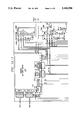
- FIGS. 1A-1 and 1A-2 show a subsystem including a microprocessor (which uses data/address multiplexing), an adjunct chip, a battery, memory, and a timekeeper chip.
- FIG. 1B shows an adjunct chip suitable for use with a microprocessor which uses data/address multiplexing.
- FIGS. 2A-1 and 2A-2 show a subsystem including a microprocessor (which does not use data/address multiplexing), an adjunct chip, a battery, memory, and a timekeeper chip.
- FIG. 2B shows an adjunct chip suitable for use with a microprocessor which does not use data/address multiplexing.
- FIG. 3A-1 shows the memory map normally used in a V40 microprocessor.
- FIGS. 3A-2, 3A-3, 3A-4, 3A-5, and 3A-6 show how the memory map of FIG. 3A-1 is preferably modified, in control mode and in user mode, for each of five different memory allocations.
- FIGS. 3B-1 through 3B-3 show memory maps and remapping for a 6303X microprocessor.
- FIGS. 3C-1, 3C-2, and 3C-3 show memory maps and remapping for an Intel 80C196 microprocessor.
- FIGS. 3D-1, 3D-2, and 3D-3 show memory maps and remapping for a Motorola 68HC11 microprocessor.
- FIGS. 3E-1 and 3E-2 show memory maps and remapping for a Hitachi 6305X2 microprocessor.
- FIGS. 4.1, 4.2, 4.3, 4.4, and 4.5 are parts of a single circuit diagram, showing the interface to one pin in the highly flexible port which is used as port A in the adjunct chip embodiments of FIGS. 1B and 2B.
- FIG. 5 shows the architecture used for ports B, C, and D, in the adjunct chip embodiments of FIGS. 1B and 2B.
- FIG. 6A shows the architecture preferably used for the multiplexed interface 186, in the adjunct chip embodiments of FIGS. 1B and 2B.
- FIG. 6B shows the architecture preferably used for the buffers 169 and 269, in the adjunct chip embodiments of FIGS. 1B and 2B (respectively).
- FIG. 6C shows the simple interface 188 preferably used for latching in high-order address bits, in the adjunct chip embodiments of FIG. 1B and 2B.
- FIG. 7 shows the architecture of the Register File Structure, which provides a very flexible interface to another computer system.
- FIG. 8A schematically shows one register of the input buffers and flags, in the Register File Structure of an adjunct chip of FIG. 1B, in the presently preferred embodiment.
- FIG. 8B shows how multiple cells as in FIG. 8A are combined to provide the full input buffer register and flag structure.
- FIG. 8C shows how multiple cells as in FIG. 8A are combined to provide the output buffer register and flag structure.
- FIG. 9A schematically shows one cell of mask register OBM.
- FIG. 9B shows how multiple cells as in FIG. 9A are combined to provide the Internal-IBM and Internal-OBM registers.
- FIG. 9C shows how multiple cells as in FIG. 9A are combined to provide the External-IBM and External-OBM registers.
- FIG. 10 schematically shows one IBIT cell of the status register.
- FIG. 11A schematically shows one cell of the AND/NOR logic which provides combinatorial masking dependence.
- FIG. 11B shows how four cells as in FIG. 11A are combined to provide the AND/NOR select options for the Internal-IBM, Internal-OBM, External-IBM, and External-OBM registers.
- FIGS. 13A and 13B show the two sides of an innovative subsystem microboard used in a preferred subsystem embodiment.
- FIG. 14 schematically shows the timing relations which assure that the adjunct chip will never be in reset when the associated microprocessor comes out of reset.
- FIG. 15 schematically shows the branches used, within the control software, to run control or reloading routines.
- the particular example shown is adapted for use with a subsystem like that shown in FIG. 16, wherein a microprocessor and an adjunct peripheral chip are combined with a modem and a DAA subsystem.
- FIG. 16 shows an example of a complete subsystem, wherein a microprocessor and an adjunct peripheral chip are combined with a modem and a DAA.
- This Figure also illustrates the physical shape of a novel preferred micro-board package.
- FIGS. 17A and 17B show the circuitry used, in the presently preferred embodiment, to implement the oscillator control circuitry 184 in an adjunct chip of FIGS. 1A-1 and 1A-2;
- FIGS. 18A, 18B, and 18C show the circuitry used, in the presently preferred embodiment, to implement the Reset Control circuits 152 in the adjunct chip of FIGS. 1A-1 and 1A-2.
- FIG. 19 shows the circuitry used, in the presently preferred embodiment, to implement the battery circuits 164 in the adjunct chip of FIG. 1A.
- FIGS. 1A-1 and 1A-2 are an overview of a first sample system embodiment employing the disclosed innovations.
- a subsystem as shown is integrated on a single sub-board with a single in-line mounting, as discussed in detail below.
- the system shown in FIGS. 1A-1 and 1A-2 includes a microprocessor 110, SRAMs 130, an adjunct chip 120, and a battery 150 which provides a constant DC power supply to the adjunct chip 120 (which can thereby power other chips when appropriate).
- the system shown also includes a watchdog chip 140. In the presently preferred embodiment, this is a DS1283 clock/calendar chip, but of course other such chips could be used instead.
- the external connections of this board include, in the presently preferred embodiment: 2
- Power-fail-detect signals V30* and V45* which indicate that the adjunct chip 120 has detected that the power supply is below corresponding threshold voltages
- Port 0 an 8-bit bidirectional port
- Port 1 an 8-bit bidirectional port
- Port A an 8-pin bidirectional port
- Port B an 8-pin bidirectional port
- Port C an 8-pin bidirectional port
- a status pin A16L which is a latched version of address bit 16. (High-order address bits A16-A19 are multiplexed, and the same pins will carry status signals during the second half of each cycle.
- the latched A16L pin allows 128K memories to receive a full address without tracking the multiplex half-cycle timing.
- the microprocessor 110 (in this example, an NEC V40 microprocessor) has ports 1 and 0 which are connected to provide data routing as desired. This microprocessor also has a multiplexed address and data port, including lines AD0 through AD7, and eight additional address lines A8 through A15. All of these 16 lines are connected to the adjunct chip 120, which is shown in greater detail in FIG. 1B.
- the presently preferred embodiment of the chip 120 corresponds to the forthcoming integrated circuit assigned to Dallas Semiconductor part number DS5340, but of course chips under this part number may subsequently be modified so that they depart from the description herein. However, the description herein provides the preferred embodiment of making and using the invention as of the time of filing this application. Of course, the innovative concepts shown in the examples herein can readily be adapted to a wide variety of other embodiments.
- 16 lines AD0 through AD7 and A8 through A15 are also connected to random access memories 130A and 130B.
- two alternative versions are shown: instead of the 8K ⁇ 8 SRAMs 130A and 130B, 32K ⁇ 8 SRAMs 130A' and 130B' may be used instead.
- the low-order address bits A0 through A7 are provided to the memories 130 from the adjunct chip 120.
- the interrupt logic 111 is connected to receive both of the interrupts INT1* and INT2*. In addition, the interrupt logic 111 is connected to receive a reset signal. However, note that this reset signal is not the same as the reset signal RST* which is externally received: The externally received reset signal is connected to the adjunct chip 120, and the adjunct chip 120 provides an RSTOUT* signal which is connected to the reset input of the microprocessor.
- the microprocessor also includes an oscillator 112.
- the XTAL and EXTAL connections of this oscillator which would normally simply be connected to a discrete crystal, are instead connected to clock terminals CLKIN and CLKOUT of the chip 120.
- the adjunct chip 120 includes two crystal connections XTAL1 and XTAL2, which are preferably connected to a crystal, not shown.
- the microprocessor 110 also includes a line RD* (which, depending on the microprocessor manufacturer, may also be referred to as a signal E or a signal DS) which is connected to an input RDIN* of the adjunct chip 120.
- RD* which, depending on the microprocessor manufacturer, may also be referred to as a signal E or a signal DS
- the microprocessor 110 also includes a WR* signal, which is connected to a WRIN* input of the adjunct chip 120.
- the microprocessor also may include an address strobe output AS, which is connected to input AST* of the adjunct chip 120.
- the adjunct chip 120 provides a write-enable output signal WROUT*, which is connected to the write-enable inputs of memory chips 130.
- the adjunct chip 120 also contains two more chip-enable outputs CE1* and CE5*, which are respectively connected to the memory chips 130A and 130B (or 130A' and 130B').
- Two additonal peripheral chip-enable outputs PCE3* and PCE4* are also provided. Note that, in the configuration shown, signal PCE3* is connected to the chip-enable input of the watchdog 140.
- PCE outputs can be used to selectively activate other peripheral chips, such as an RF interface, or can optionally be led to an external connection for control of other portions of the system.
- the adjunct chip 120 also provides address line outputs A0 through A7, and receives a battery input voltage VBAT. Ports B and C are led directly off-chip. In addition, an IBMINTE* output is also provided, as will be described below.
- FIG. 2A shows another sample system configuration, using a microprocessor 210 which does not multiplex data with addresses.
- the overall configuration of this system is generally similar to that of FIG. 1A, but there are some differences which should be noted.
- the adjunct chip 220 preferably used in such a system is slightly different from the adjunct chip 120, as shown in detail in FIG. 2B.
- FIG. 2B may be seen to generally be similar to FIG. 1B. In general, corresponding elements have been given the same number. However, note that buffer 269 is an 8-bit-wide address input register, whereas buffer 169 is an 8-bit-wide address output register. Also note that the Port D interface 262 is now used for a full 8-bit bidirectional port, whereas in the example of FIG. 1B this port was used for additional data and control lines. Of course, the data lines at this port can stil be used, if desired, to carry comparable control and status information.
- the adjunct chip 220 is the integrated circuit which is commercially available under part number DS5303 from Dallas Semiconductor Corporation.
- the commercially available integrated circuit may be changed over time, and the description set forth herein defines the presently preferred embodiment as of the time of filing the present application.
- CMOS microprocessors have a sleep mode, where the processor will consume minimum standby power when no computation is needed.
- the disclosed adjunct chip architecture permits this sleep mode to be exploited as well as if the microprocessor were in a standalone configuration.
- the softener redirects addresses as follows: when the microprocessor tries to access an initial address in program RAM, the adjunct chip revectors this access so that the microprocessor is reading out (and executing) the start-up code which is stored in the adjunct chip's ROM.
- ROM read only memory
- code contained in ROM is used for two major functions:
- the adjunct chip also includes 16 bytes of internal RAM which are only accessible by the control software, not by the user software. In the presently preferred embodiment, this RAM is further protected by timed-access relationships. These bytes are used to store the high and low boundaries for
- the adjunct chip provides both software and hardware avenues to enter execution of the control software.
- execution of control software can be started in the following ways:
- Bit CRC indicates whether the CRC routines are to be executed.
- FIG. 15 is a schematic flow chart which shows generally the program flow in the control-software routines.
- the ROM memory in the adjunct chip can be accessed when the microprocessor powers up, and a CRC check then run on the user program, in external RAM.
- the adjunct chip itself contains hardware for generating the Cyclic Redundancy Check (CRC) check value.
- CRC Cyclic Redundancy Check
- the microprocessor merely has to read out the data values in the range to be checked, and push them successively into a register address.
- the softener hardware captures writes to this address, and loads the stream of values into its CRC hardware.
- the microprocessor can fetch the computed CRC value by simply reading another "register,” at a register address which is remapped into the softener.
- the microprocessor never has to do the multiplies necessary for CRC computation: it simply performs a series of register writes, a 16-bit register read, and a compare operation. This speeds up CRC generation, and allows system software designers to use CRC checking more readily.
- the arguments for CRC check operations include high- and low-address boundaries, which are kept in the adjunct chip's on-chip RAM. (This RAM is only accessible when the microprocessor is executing code from ROM.) Thus, when a CRC operation is initiated, the designated block of memory will be processed to generate a CRC redundancy check value.
- the RL* input which is used to control reloads, is not purely a logic level.
- a reload command causes a reset, which then branches into the adjunct chip's ROM address space.
- the adjunct chip will again reset the target microprocessor, and execution can then begin in the user's program memory.
- control software can be exited in the following ways:
- the memory map as seen by the microprocessor, will differ depending on whether the microprocessor is running control software or user software. Moreover, the memory maps used are different for the various target microprocessors.
- FIG. 3A-1 shows the memory map normally used in a V40 microprocessor. Addresses from 00000 H 3 to 00400 H are normally used for interrupt vectors. Addresses from 00400 H to FFFF0 H are available for data or program memory. Addresses FFFF0 H through FFFFC H are used for reset information, and the remaining higher addresses are reserved.
- FIGS. 3A-2, 3A-3, 3A-4, 3A-5, and 3A-6 show five modes of operation. These modes are selectable to accommodate various memory configurations.
- FIG. 3A-2 shows control and user software operating modes in mode 0, where the RAM configuration is two 32K ⁇ 8 memories.
- FIG. 3A-3 shows control and user software memory assignments for a system which has five 32K ⁇ 8 RAMs. (In this configuration, a full 1M (20 bits) of address space is available. The five 32K memories pick up only a fraction of this address space, and the remainder is available for use by external memory. The five 32K memories are each separately controlled by chip-enable lines CE1* through CE5*.
- FIG. 3A-4 shows an operating mode which is generally similar to that of FIG. 3A-3, except that four 128K ⁇ 8 memories and one 32K memory are used. Thus, 480K remain for external memory.
- FIG. 3A-5 shows memory mapping for a case where chip-enable signals CE1*, CE2*, CE3*, CE4*, and CE5* each control a 128K memory.
- FIG. 3A-6 shows control and user software memory maps for Mode 4, wherein CE1* controls a 128K ⁇ 8 memory, CE2* controls a 512K ⁇ 8 memory, and CE5* controls a 32K ⁇ 8 memory. Thus, in this example, 352K of address space remains to be allocated to external memory.
- FIGS. 3B-1 through 3B-3 show memory maps used with a 6303X microprocessor. (This is the microprocessor shows in the example of FIGS. 2A-1 and 2A-2. However, it is now contemplated that use of the 6303Y microprocessor may be more advantageous.)
- FIG. 3B-1 shows the basic memory map of the HD6303X. Addresses from 0000 H to 0020 H are used for internal registers. Addresses from 0020 H to 0040 H and 0100 H to FFEA H are used for external memory. Addresses 0040 H to 0100 H are used for internal random access memory. Addresses FFEA H to FFFF H are used for interrupt and reset vectors.
- FIG. 3B-2 shows how this address space is reallocated in a first mode, where 16K bytes are controlled by chip enables CE1* and CE2*, in control software operation and user software operation.
- FIG. 3B-3 shows how the 64K of address space of the 6303 is remapped in a different operating mode, wherein 64K bytes of RAM are locally available. In this case, note that no space for external memory is available.
- FIGS. 3C-1, 3C-2, and 3C-3 show remapping for an Intel 80C196 microprocessor. As shown in FIG. 3C-1, the basic memory map of this microprocessor is 64K, and is mapped as shown.
- FIG. 3C-2 shows how this memory space is remapped in a system which combines an 80C196 with an adjunct chip as disclosed herein, in a module which includes two 8K ⁇ 8 RAMs.
- Addresses 0000 H to 0020 H are used for 80C196 data memory, SFRS, and stack pointer.
- Addresses 0020 H to 0080 H are used for CE1-RAM.
- Addresses 0080 H to 0100 H are used for 80C196 internal RAM.
- Addresses 0100 H to 0200 H are used for CE3- or CE1-RAM.
- Addresses 0200 H to 0300 H are used for CE4- or CE1-RAM.
- Addresses 0300 H to 0340 H are used for adjunct-chip registers (64 bytes).
- Addresses 0340 H to 1FFE H are used for CE1-RAM. Addresses 1FFE H to 2000 H are used for Port 3 and Port 4. Addresses 2000 H to 3000 H are used for reset/interrupt vectors, configuration byte, and adjunct-chip bootstrap ROM (3968 bytes). Addresses 3000 H to 4000 H are used for CE2-RAM. Addresses 4000 H to FFFF H are used for external memory.
- FIG. 3C-3 shows how the memory space is remapped in a slightly different embodiment, which includes 32K of memory directly controlled by the adjunct chip. Note that no memory space, in this version, is available for external memory.
- FIG. 3D-1 shows the basic memory map of a Motorola 68HC11 microprocessor. Again, note that this is a 64K memory map. Addresses 0000 H to 0100 H are used for internal RAM. Addresses 0100 H to 1000 H , 1040 H to B600 H , B800 H to BF40 H , C000 H to E000 H , and E000 H to FFC0 H are available for external memory. Addresses 1000 H to 1040 H are register block. Addresses B600 H to B800 H are used for 512 bytes EEPROM. Addresses BF40 H to C000 H are used for special mode ROM/vectors. Addresses FFC0 H to FFFF H are used for interrupt and reset vectors.
- FIG. 3D-2 shows a memory map for a module which includes this microprocessor with an adjunct chip as disclosed, and two 8K ⁇ 8 SRAMs in the module. In this case, some memory space remains accessible by external memory. Note also that chip enables CE3* and CE4* control memory which is mapped onto portions of the memory space.
- FIG. 3D-3 shows a memory map for another version, which is generally similar to the version of FIG. 3D-2 except that two 32K memories are used. Note that, in this case, no address space remains for external memory.
- FIG. 3E-1 shows the basic memory map for a Hitachi 6305X2 microprocessor. Addresses 0000 H to 0020 H are used for internal registers. Addresses 0020 H to 0080 H , 0100 H to 1FF6 H , and 2000 H to 3FFF H are used for external memory. Addresses 0080 H to 0100 H are used for internal RAM. Addresses 1FF6 H to 2000 H are used for interrupt and reset vectors.
- FIG. 3E-2 shows memory address allocations, in control software operation and user software operation, for a system which combines a 6305 microprocessor with a matched adjunct chip as described herein.
- two 8K ⁇ 8 RAMs are available, controlled by chip-enable outputs CE1* and CE2*.
- Addresses 0000 H to 0020 H are used for internal registers.
- Addresses 0020 H to 0080 H are used for CE1-RAM.
- Addresses 0080 H to 0100 H are used for internal RAM.
- Addresses 0100 H to 0200 H are used for CE3- or CE1-RAM.
- Addresses 0200 H to 0300 H are used for CE4- or CE1-RAM.
- Addresses 0300 H to 0340 H are used for adjunct-chip registers (64 bytes). Addresses 0340 H to 1000 H are used for CE1-RAM. Addresses 1000 H to 1FF6 H are used for adjunct-chip bootstrap ROM (4086 bytes. Addresses 1FF6 H to 2000 H are used for reset/interrupt ROM. Addresses 2000 H to 3FFF H are used for CE2-RAM.
- FIG. 3E-3 shows a slightly different assignment, where addresses 0000 H to 0020 H are used for internal registers. Addresses 0020 H to 0080 H are used for CE1-RAM. Addresses 0080 H to 0100 H are used for internal RAM. Addresses 0100 H to 0200 H are used for CE3- or CE1-RAM. Addresses 0200 H to 0300 H are used for CE4- or CE1-RAM. Addresses 0300 H to 0340 H are used for adjunct-chip registers (64 bytes). Addresses 0340 H to 1FF6 H are used for CE1-RAM. Addresses 1FF6 H to 2000 H are used for reset/interrupt CE1-RAM. Addresses 2000 H to 3FFF H are used for CE2-RAM.
- the microprocessor is not only able to access Port 0 and Port 1 as usual, but can also make use of ports A-D on the adjunct chip, as described below, by setting the appropriate register bits in the adjunct chip.
- microprocessor can also use the adjunct chip to provide programmable interrupt-masking, as described below.
- the adjunct chip also provides smart control of microprocessor sleep mode and resets, as described below.
- FIG. 1B shows the overall architecture of the adjunct chip 120 shown in FIGS. 1A-1 and 1A-2.
- the adjunct chip can exist in several different versions, which each have slightly different features (implemented by simple mask options), depending on which target microprocessor is to be used.
- five different versions of the adjunct chip are contemplated, aimed at five different families of target microprocessor.
- further versions of the adjunct chip can also be added, with other target microprocessors.
- adjunct chip can provide great versatility in the device-level architecture of the target microprocessor.
- the CMOS adjunct chip can be combined with an NMOS, or even bipolar, target microprocessor to provide a low-power and crash-proof system.
- the five target architectures presently planned for use are the following:
- the NEC V40 microprocessor This is the presently preferred embodiment and will be primarily referred to in the detailed description below.
- the NEC V40 is generally similar to an Intel 8086, but without on-chip memory or ports.
- the Intel 80C196 (a redesign of the 8096 architecture) is a 16-bit microcontroller, which is extremely fast.
- Hitachi 6305 This chip is generally similar to the Motorola 6805. It has a 16K address map.
- a reset and interrupt control 152 can receive interrupts on pins INT1* and INT2*, and can also output interrupts on those pins, in order to direct interrupts to the microprocessor 120.
- logic block 152 is also connected to receive externally generated resets and to send resets to microprocessor 110 on line RSTOUT*.
- Reload control logic 154 receives the external input RL*, which can command initiation of a reload, as described below.
- FIGS. 18A, 18B, and 18C show the circuitry used, in the presently preferred embodiment, to implement the reset and Interrupt Control circuits 152 in the adjunct chip of FIGS. 1A-1 and 1A-2.
- Battery circuits 164 include freshness seal logic 165, a current source 166, and a bandgap voltage reference 167.
- the circuit block 164 receives both a battery voltage VBAT and a system power supply voltage VCCI as inputs, and can detect failure of the system power supply voltage accurately with reference to the bandgap voltage reference 167.
- the circuit block 164 also provides the power output V CC which powers the other circuits on-chip.
- the circuit block 164 also includes comparators, which can detect variation in the level of the system supply voltage VCCI. In the embodiment shown, this circuit block also generates two logic output signals, which can be used to switch other devices or to provide warnings or interrupts to other ICs or subsystems in the same system of imminent power failure.
- signal V45* indicates that the power supply VCCI has fallen to 4.5 volts, and that shut-down procedures should therefore be initiated.
- Signal V30* indicates that the system voltage has fallen to 3.0 volts, and that parts having a battery voltage input should therefore switch over to battery backup for data maintenance.
- FIG. 19 shows the circuitry used, in the presently preferred embodiment, to implement the battery circuits 164 in the adjunct chip of FIGS. 1A-1 and 1A-2.
- the address bus 168 is also received by a "reload and reset-vector ROM" 174.
- This block of ROM contains the control software routines for reloading and CRC check, discussed above.
- This block of ROM also includes the reset-vector memory, which is a small amount of memory (16 bytes, in the presently preferred embodiment) at the address first accessed by the microprocessor after a reset. This is normally used for a long jump instruction.
- An address bus 168 and a data bus 170 are routed around the chip.
- the address bus and data bus are both 8-bits wide.
- An address output buffer 169 can be selected to externally output the addresses on the address bus 168.
- the address bus 168 is also received by internal registers and port controls (block 176). This block also has a bidirectional connection to data bus 170.
- address/data multiplexed interfaces 186 are also interfaced to the address bus 168 and to data bus 170, under control of the signals RDIN*, WRIN*, and AST*.
- Latches 188 latch in the high-order address bits A8 through A15.
- This circuitry is merely a straightforward use of conventional address decoder architecture.
- the only unusual feature is that an additional bit CESL is introduced into the decoder. This bit provides the additional input to implement the sliding address overlay.
- the clock output of the microprocessor (CLKIN) is received by a stop detect and watchdog circuit 182.
- CLKIN The clock output of the microprocessor
- the adjunct chip In addition to the clock monitor circuit, the adjunct chip also contains a watchdog function. This function, too, is made programmable. Thus, the user can determine what period of inactivity the watchdog function should wait for before activating a reset or interrupt.
- the watchdog function is always active when the microprocessor is being operated from adjunct chip ROM.
- the watchdog parameters include user-programmable options: For example, the inactive time required before the watchdog activates a reset is programmable. Moreover, the watchdog can optionally be turned off.
- a clock oscillator control 184 is connected to the crystal terminals XTAL1 and XTAL2 and provides switching from the crystal stabilized oscillation to a ring oscillator clock on power-down, as will be described later.
- FIGS. 17A and 17B show the circuitry used, in the presently preferred PG,126 embodiment, to implement the oscillator control circuitry 184 in an adjunct chip of FIGS. 1A-1 and 1A-2.
- the address and data buses 168 and 170 are also connected to a register file 180.
- this register file 180 is externally interfaced through ports B and C. This register file provides an extremely versatile control interface.
- the Interface Register File on the Adjunct chip is designed to provide an asynchronous interface between two independent microprocessors.
- the microprocessor which is connected as the controller of the Adjunct chip is able to transform two of the normal ports of the adjunct chip into a PC bus compatible address/data bus interface. This interface allows an external microprocessor such as an 8088 to asynchronously access internal registers on the Adjunct chip. These registers are broken into four configurations:
- Each microprocessor interface is assigned one status register which serves as a general purpose register with which each processor communicates configuration information to the other processor to establish a file protocol.
- the I/O Buffer Registers are the actual registers by which the data transfers are made.
- Eight Input Buffer and eight Output Buffer registers are assigned to each processor. This allows each processor to work in either a single register or block data transfer configuration.
- Each processor can also read two flag registers to monitor the status of each read and write of both the Input and Output Buffer Registers.
- Two Interrupt Mask Registers are also assigned to each processor. The two Interrupt Mask Registers assigned to each processor allow each processor to selectively mask or unmask specific register flags as sources of interrupts to itself.
- the interface register file includes the following registers:
- ISR Internal Status Reg.
- ESR External Status Reg.
- IBR Input Buffer Reg.
- the internal status register is composed of four status bits (ST3-ST0), an internal to external interrupt bit (I1), an external to internal interrupt mask (M2), and two AND/OR control bits (IAO and OAO) for input and output buffer flag interrupt configurations.
- the Internal Status Register is configured as a full read/write register to the internal processor.
- the internal register is a read only register to the external processor, except for the I1 bit.
- Bit M2--The M2 interrupt mask blocks the I2 interrupt from external status register as issued by the external processor (to the internal processor).
- the internal processor is able to write a status word into the status bits and set the interrupt bit which in turn will interrupt the external processor if the M1 mask bit in the external status register is cleared. Once an interrupt has been issued, the external processor can clear the interrupt by writing to the internal status register which automatically clears the I1 bit. It is important to note that a write by the external processor to the internal status register is independent of data, will not alter other bits, and will only clear the I1 bit. Once the I1 bit has been set by the internal processor it can only be cleared by either the external processor or a Reset. The internal processor is not able to clear the I1 bit once it is set.
- the mask bit M2 is used to block the interrupt issued by the external processor by the I2 bit in the external status register.
- the internal processor can receive an interrupt as a function of the reading and writing of the Input and Output Buffers.
- the reading and writing of these buffers provide interrupts in either a byte or block interrupt mode. This selection is provided through the use of the OAO or IAO bits.
- the IAO and OAO bits are used to allow the internal processor to select an AND or an OR relationship in relation to when an interrupt will be issued via the appropriate mask register. Setting the OAO bit to a one initiates the AND relationship and setting it to a zero initiates the OR mode.
- the OAO bit In the AND mode the OAO bit requires that all of the Output Buffer Registers, which are not masked in the Internal Output Buffer Mask Register, be read by the external processor before an interrupt will be issued to the internal processor.
- the OR mode the OAO bit initiates or continues an interrupt each time an Output Buffer register, which is not masked in the Internal Output Buffer Mask Register, is read by the external Processor.
- the IAO bit When in the AND mode the IAO bit requires that all of the registers in the Input Buffer, which are not masked in the Internal Input Buffer Mask Register, be written by the external processor before an interrupt will be issued to the internal processor.
- the IAO bit In the OR mode the IAO bit allows an interrupt to the internal processor whenever any Input Buffer register, which is not masked in the Internal Input Buffer Mask Register, is written by the external processor.
- both the Output and Input Buffers are configured as read before write registers.
- a write to the Input Buffer by the external controller is only completed by the Softener when the Input Buffer has been previously read by the internal processor. This prevents a potential loss of data which could occur if the external processor were to attempt to write over the Input Buffer before the internal processor has read the previous data in the Input Buffer.
- the Input and Output registers are also configured to provide correct data if read when the appropriate flag is set in the Input and Output Flag register. As a result once a buffer has been read by the appropriate processor and the related flag is cleared, future reads of the same buffer can not be considered valid until the respective flag is again set by a new write from the appropriate processor.
- the external status register is composed of four status bits (ST3-ST0), an external to internal interrupt bit (I2), an internal to external interrupt mask (M1), and two AND/OR control bits (IAO and OAO) for input and output buffer flag interrupt configurations.
- the External Status Register is configured as a full read/write register to the external processor.
- the external register is a read only register to the internal processor except for the I2 bit.
- Bit I2 is the external processor to internal processor interrupt control bit.
- Bit M1 is an interrupt mask which blocks the I1 interrupt from internal status register as issued by the internal processor (to the external processor).
- Bit OAO is the output buffer AND/OR interrupt control select.
- Bit IAO is the input buffer AND/OR interrupt control select.
- Bits ST3-ST0 are general purpose status register bits written by the external processor to the internal processor.
- the external processor is able to write a status word into the status bits and set the interrupt bit which in turn will interrupt the internal processor if the M2 mask bit in the internal status register is cleared. Once an interrupt has been issued, the internal processor can clear the interrupt by writing to the external status register which automatically clears the I2 bit. It is important to note that a write by the internal processor to the external status register is independent of data, will not alter other bits, and will only clear the I2 bit. Once the I2 bit has been set by the external processor it can only be cleared by either the internal processor or a Reset. The external processor is not able to clear the I2 bit once it is set.
- the mask bit M1 is used to block the interrupt issued by the internal processor by the I1 bit in the internal status register.
- the external processor can receive an interrupt as a function of the reading and writing of the Input and Output Buffers.
- the reading and writing of these buffers provide interrupts in either a byte or block interrupt mode. This selections is provided through the use of the OAO or IAO bits.
- the IAO and OAO bits are used to allow the external processor to select an AND or an OR relationship in relation to when an interrupt will be issued via the appropriate mask register. Setting the OAO bit to a one initiates the AND relationship and setting it to a zero initiates the OR mode.
- the OAO bit In the AND mode the OAO bit requires that all of the Output Buffer Registers, which are not masked in the External Output Buffer Mask Register, be written by the internal processor before an interrupt will be issued to the external processor.
- the OR mode the OAO bit initiates or continues an interrupt each time an Input Buffer register, which is not masked in the External Output Buffer Mask Register, is written by the internal Processor.
- the IAO bit When in the AND mode the IAO bit requires that all of the registers in the Input Buffer, which are not masked in the External Input Buffer Mask Register, be read by the internal processor before an interrupt will be issued to the external processor.
- the IAO bit In the OR mode the IAO bit allows an interrupt to the external processor whenever any Input Buffer register, which is not masked in the External Input Buffer Mask Register, is read by the internal processor.
- FIGS. 1A-1, 1A-2, 2A-1, and 2A-2 note that specific allocations are made of 64 addresses for use within the adjunct chip.
- those 64 addresses may not appear in the same place for the different memory maps of FIGS. 3A through 3E.
- Many of those microprocessors have internal RAM, or internal registers at fixed addresses, and these address allocations must be respected. Therefore, the addresses onto which the 64 bytes required for internal space are mapped may be changed. For example, in the DS5303 (for use with the 6303 microprocessor) these internal addresses are mapped onto microprocessor addresses 0300 H through 0340 H , in all modes. With the 6305 microprocessor. The same address mapping is used in FIGS. 3C, 3D, and 3E.
- mapping can be changed if those addresses are not accessible. For example, in the memory map of FIGS. 3A-1 through 3A-6, these 64 bytes are mapped onto addresses FFF00 H through FFF40 H . Therefore, in the following list, these registers will be named only by their least significant two nibbles (two hex characters).
- Address 16 (address 10 H ) is used for the timed access register TASR.
- the microprocessor For access to memory which is protected by a timed access relationship, the microprocessor must write a value of 170 (AA H ) to its register, followed by a value of 85 (55 H ).
- Port A interrupt mask register (PTMK). This mask register contains 8 mask bits M7 through M0 which mask the corresponding 8 bits of Port A.
- Address 18 (12 H ) is a memory control register.
- Four bits PA0-PA3 of this register are used memory-protection bits, to indicate which segment of memory are write-protected.
- Two bits are used for signals PCE3* and PCE4*, which provide chip enables.
- Address 19 (13 H ) is a watchdog register (WDOG).
- WDOG watchdog register
- three bits (WD0-WD2) are used for selecting the watchdog time-out value. These bits are writable only when the control software is running, and not when the user software is running.
- Additional bit WBM is used for a watchdog mask. This bit can turn on or turn off sensitivity to a watchdog interrupt. Setting of this bit is protected by a timed access relationship.
- An additional bit is the CRC bit, which forces execution of a CRC routine on a power-on reset or a watchdog hit. This bit is protected by a timed-access relationship and is writable only when the control software is executing.
- An additional bit is bit ROMLTR.
- the bit ROMLTR is protected by timed-access relationships. Moreover, this bit is writable only when control software is executing, and only when the external reload pin RL* is active.
- Address 20 (address 14 H ) is a modes register (“MODES”), and contains bits which set several important features of operation:
- Bit RG is used to define at what point the address boundary between RAM controlled by output CE1* and RAM controlled by output CE2* will occur in microcontrollers. This bit is writable only from control software, and is protected by a timed-access relationship.
- Bit PART is a partition-enable signal. This bit enables write-protection of memory. 4 This bit is protected by a timed-access relationship and is ROM writable only.
- Bit RFEN is a register file enable bit. This is protected by a timed-access relationship.
- Bits MD0-MD2 selected the mode of memory map. These bits would be used to select between the memory maps of 3A-2 and 3A-6, for operation with a V40 microprocessor. These bits are writable only from control software and are protected by a timed-access relationship.
- Bit IRL is an internal reload flag. This indicates that the external reload pin RL* is active.
- Bit ROM is the bit which enables execution of control software (the "ROM-enable" bit). As noted, this bit is extremely important to the operation of the system FIGS. 1A-1, 1A-2, or 2A-1, 2A-2. Writing of this bit is protected by a timed-access relationship. Thus, as extensively discussed above, the user software can write this bit to enter execution of control software. Changing the state of this bit may cause the adjunct chip to throw the microprocessor into reset, as described below.
- Address 21 (15 H ) contains bits relating to power control functions. This register is also referred to in the accompanying circuit diagrams as Register "POWER.”
- Bit CESL is an inversion control for bits A13-A15. These bits are inverted in the address decoder to permit program memory underneath the control ROM to be executed.
- Bit SPLITWD provides an input into the middle of the watchdog chain, which accelerates testing. This bit is writable in test mode only, and otherwise will be cleared.
- Bit CEBAT enables battery backup for outputs CE2*, CE3*, and CE4*. If this bit is set, then output lines CE2* through CE4* will be connected to the battery input, to be powered from battery 150 if system power VCCI goes down. Since these bits are active low, they would normally be high in standby mode. If the RAM's internal circuitry permits it to thieve power from the CE line, then this output will permit the RAM's data to be preserved. This output is writable only from the control software, and is protected by a timed-access relationship.
- Bit LPE is a low-power enable. This allows the adjunct chip to go into a low-power (sleep) state when the microprocessor stops. 5 This bit is protected by a timed-access relationship.
- Bit LVM is a low-voltage mask bit, which masks the LVD interrupt described below. This bit is protected by a timed-access relationship.
- Bit BATTEST turns on an op amp to check the battery voltage against the bandgap voltage reference.
- Bit BAT is a battery health flag. This bit is controlled by hardware (from comparators).
- Address 22 (16 H ) is a reset and interrupt status register (“RIST"). This register also contains several flag bits which relate to various control functions.
- Bit WDR is a watchdog reset bit. This is a write-only bit which is cleared automatically as soon as it is written. This bit is protected by a timed-access relationship.
- Bit WDS is a watchdog status flag. This is cleared when read.
- Bit LVD is a low-voltage detect flag. This bit is set by hardware, whenever comparison of VCCI against the bandgap voltage reference indicates that VCCI is out of tolerance. It is cleared when read. 6
- Bit PUP is a power-up indicator flag. This bit is cleared on any power-up reset. This bit can be set by software (if a timed-access relationship is satisfied). Thus, if a user sets this bit routinely, he can test it after a reset to ascertain whether the reset was a power-up reset.
- Bit RFSTS is register filed status register interrupt.
- Bit IB is a register file input buffer interrupt.
- Bit OB is a register film output buffer interrupt.
- Bit PA is a Port A interrupt.
- Addresses 23 through 30 (17 H through 1E H ) are used for control of Port A.
- Address 23 (17 H ) is Port A's data latch register.
- Address 24 (18 H ) is the data direction register.
- Address 25 (19 H ) is the modo-Intel register, i.e., selects between Motorola and Intel emulation.
- Address 26 (1A H ) is a port pinwrite register and is read only (from the adjunct chip).
- Address 27 (1B H ) is an edge-detect register and is read-only (from the adjunct chip).
- Address 28 (1C H ) is a level detect register and is read only (from the adjunct chip).
- Address 29 (1D H ) selects between edge detect and level detect.
- Address 30 (1E H ) selects between positive and negative actuation, on the edge detect and level detect functions. Note that each of these registers has 8 bits, and thus the settings of these registers can be used to control the port on a bit-by-bit basis. Therefore, these registers provide tremendous versatility in controlling the operation of Port A.
- Addresses 31 through 35 (1F H through 23 H ) provide the interface to Port B.
- Addresses 36 through 40 (24 H through 28 H ) provide the interface to Port C.
- Addresses 41 through 45 (29 H through 2D H ) provide the interface to Port D.
- Address 31 (1F H ), 36 (24 H ), and 41 (29 H ) are data latch registers and are read/write.
- Address 32 (20 H ), 37 (25 H ), and 42 (2A H ) are data direction registers and are read/write.
- Addresses 33 (21 H ), 38 (26 H ), and 43 (2B H ) are Motorola-Intel-select registers, and are read/write.
- Addresses 34 (22 H ), 39 (27 H ), and 44 (2C H ) are port pin registers and are read only. Addresses 35 (23 H ), 40 (28 H ), and 45 (2D H ) are edge-detect registers and are read only.
- a zero-bit is used, in the presently preferred embodiment, to indicate that the data direction is in, and a "1" is used to indicate that the data direction is out.
- a "0" is used to select Intel emulation, and a "1" selects Motorola emulation.
- edge/level select registers In the edge/level select registers, in the presently preferred embodiment, a "0" is used to select edge-detect, and a “1” is used to select level-detect. In the positive/negative select register, a “0” is used to select negative operation, and a “1” is used to select positive operation. In the edge/level detect registers, a "0” means that no edge or level has been detected, and a "1" indicates that an edge or level has been detected. Addresses 2E H and 2F H (46 and 47) are the CRC registers. CRC computation is performed in hardware.
- Address 47 (2F H ) is read, a series of writes is made to Address 46 (E H ), and then another read is made to Address 47 (2F H ) to get the updated CRC value.
- addresses 48 through 63 (30 H through 3F H ) are reserved for internal RAM, as described below.
- the reset values for the registers are as follows:
- the timed-access register TASR is reset to all zeroes.
- the Port A interrupt mask register PTMK is reset to all ones.
- the memory-control register has bits PA0-PA3 cleared on a no-battery reset and otherwise unchanged. Bits PCE3*-PCE4* of this register are set to zero on a reset.
- the watchdog register WDOG has bits WD0-WD2 set to zero on a no-battery reset, and otherwise left unchanged.
- Bit WDM is set to one on a no-battery reset, and otherwise left unchanged.
- Bits CRC and ROMLTR are set to zero on a no-battery reset and otherwise left unchanged.
- the modes register "MODES" has bits RG, PART, and MD0-MD2 set to a zero on a no-battery reset and otherwise left unchanged.
- Bit RFEN is set to zero on a reset.
- Bit IRL is left unchanged on a reset.
- Bit ROM is set to zero on a power-on reset and otherwise left unchanged.
- the power control register "POWER" bit CSL is set to zero when the control mode is exited by clearing the ROM bit. On any reset, other than a reset which occurs when the ROM bit is set, this bit will be cleared. Bit SPLITWD is cleared on any reset, except in test mode.
- Bits CEBAT and LPE will be set to zero on a no-battery reset, and otherwise left unchanged.
- Bit LVM will be set to a one.
- Bit BATTEST will be set to a zero.
- bit WDS will be set to zero on a no-battery reset, and otherwise left unchanged.
- Bits LVD and PUP will be set to zero on a power-on reset, and otherwise left unchanged.
- Bits WDR, RFSTS, IB, OB, and PA will be set to zero.
- the softener chip also includes a small amount of parameter RAM, which is used to preserve the status of various programmable options.
- this RAM includes only 16 bytes, which are organized in two blocks: Each holds a start address, an end address, and a CRC value.
- the watchdog program like other programmable options, needs to be insulated against accidental corruption by application software.
- Several techniques are used to provide such protection:
- the adjunct chip includes 4K of ROM. Of course, more or less space could be used if desired.
- Interfaces 156, 158, 160, and 162 provide 8-bit interfaces to ports A through D respectively.
- Ports A, B, and C each provide bidirectional IO capability.
- Port D is dedicated to control signals and high-order address signals, as described below.
- One of the features of the preferred adjunct chip architecture is that one of the ports is made extremely versatile and programmable. To ensure that port versatility is not lost, the preferred embodiment of the adjunct chip contains one port (Port A) which has extraordinarily high versatility. This port is programmable bit-by-bit to emulate a very wide variety of port characteristics.
- each port is electrically configurable as read or write.
- three strengths of pull-up are attached to each port: (1) a very strong pull-up, controlled by a one-shot, which initially writes a high state to the contact pad; (2) a very weak pull-up, which holds the contact pad high when a high state is being written, after the one-shot delay has expired and turned off the strong pull-up; and (3) a weak pull-up, which is the feedback of the data input latch.
- a simple, direct NMOS pull-down is used for driving this port in the opposite direction.
- the microprocessor simply writes a high state and then waits for an external input to drive data onto the port (overriding the weak pull-up if necessary).
- the normal Motorola port simply uses a direct CMOS driver at the output, in combination with a data direction register which can disable the output driver.
- the Motorola 6805 port architecture actually provides the capability to read the data latch independently of the voltage of the pad.
- a data-direction register bit is used to indicate whether the pad is being read from or written to, and the value of this bit gates the input to the data latch. Thus, if the data-direction register indicates that data is inbound, the read line will show the data appearing on the pad; but if the data-direction register indicates that data is outbound, the read line will merely show the data last latched in.
- the port implemented in the adjunct chip can implement either full Motorola or full Intel port relationships.
- this port has the capability to read either the pad or the data register, independently of the data direction.
- the innovative port provides the capability for full Motorola emulation, and also provides additional flexibility.
- This port also has the ability to sense an edge transition, of either sign, or to sense a level of either sign (as long as it remains for more than one bus cycle) and to generate interrupts therefrom, in accordance with mask bits.
- the ability to sense edges is particularly useful, since one problem with microprocessor ports in general is that some input signals may generate an edge at the microprocessor port which does not correspond to a long-term level shift. The sampling time of the microprocessor may be long enough, that such a pulse could be missed.
- the port may further be made programmable to include additional options, such as an "inverse Intel" port (with graduated-strength pull-downs), or a combination of an Intel port with a high impedance state.
- additional options such as an "inverse Intel" port (with graduated-strength pull-downs), or a combination of an Intel port with a high impedance state.
- ports C and D are identical.
- Port B is almost identical to ports C and D, except that port B defaults to the Motorola state after a reset.
- ports B and C are used for the file register, and port D is used to handle additional control lines of the microprocessor.
- ports B, C, and D are a subset of the capabilities of port A.
- Ports B, C, and D cannot do level detect; can only detect negative edges; cannot generate an interrupt; but can switch between Motorola and Intel operation.
- the adjunct chip has a low-power sleep mode, which it can enter when the target microprocessor is asleep. It would be wasteful for the adjunct chip to remain in an active high-power mode if the microprocessor has gone into a low-power sleep mode.
- the following discussion relates not only to issues of shutting down and waking up the microprocessor, but also to issues of shutting down and waking up the adjunct chip.
- adjunct chip When the adjunct chip enters sleep mode, it will typically interrupt the oscillator clock to the microprocessor; interrupt reset signals to the microprocessor; and turn off the watchdog circuit. Also, on entering sleep mode, the op amp's current source is turned down. This causes the op amp to react more slowly.
- a signal called "STOP" is used on the adjunct chip to control these functions. However, this signal is not externally accessible.
- the adjunct chip in the presently preferred embodiment, also includes a clock monitor circuit as described above, which monitor electrical activity on the microprocessor's output lines. If a certain number of clocks (selectable up to 2 10 , in the presently preferred embodiment) pass with no activity whatsoever on the microprocessor's clock-output line, the adjunct chip can assume that the microprocessor has gone to sleep.
- the microprocessor is not directly connected to a clock. Instead, the adjunct chip is interposed between the microprocessor and its clocks. Similarly, the adjunct chip is interposed between the microprocessor's reset input and the external reset connection.
- the adjunct chip when the adjunct chip determines that the microprocessor is in sleep mode, the adjunct chip can turn off clock pulses to the microprocessor. Similarly, when the microprocessor is to wake up again, the adjunct chip can restart the oscillator, and wait for the oscillator to stabilize, before connecting the oscillator to the microprocessor.
- the oscillator will normally have a significant current burn, and it is desirable to avoid this when the system is in a minimum-power mode.
- adjunct chip also has a mask option whereby the microprocessor will be awakened if an interrupt is received.
- Other conditions wherein the target microprocessor will be reawakened include detection of a power-down condition (as described below) or a reload operation.
- the band-gap voltage reference In sleep mode, the band-gap voltage reference is switched off. Instead, in sleep mode, the battery input is used as the reference input to comparators.
- the watchdog function is turned off when the adjunct chip is in sleep mode.
- the adjunct chip in the presently preferred embodiment, can be forced into test mode by driving external reset line RST* low, and also overdriving reset-out line RSTOUT* high (fighting the adjunct chip's drivers). After a certain minimum time, this will put the adjunct chip into test mode. Test mode is not normally used by end-users. The input into the middle of the watchdog's chain allows the various outputs of the watchdog chain to be tested rapidly, without having to wait for the delays needed to count down for the many cycles which would otherwise be necessary. A further feature in test mode is that the delay normally imposed at power-up is disabled.
- FIG. 16 shows the preferred microboard package for a system like that shown in FIGS. 1A-1, 1A-2, or 2A-1, 2A-2.
- a particularly advantageous system embodiment is a combination of a nonvolatized microprocessor module (such as the DS2340 described below) in combination with other modules which permit dial-up access. For example, this is permitted by a DS2245 modem Stik in combination with a DS2249 DAA Stik.)
- the 16 bytes of RAM on the adjunct chip are used not only to store CRC parameters, but also are used to store a modem-present flag and a "help-me" flag.
- the modem-present flag is programmed at the time of system configuration to indicate to the adjunct chip's control software that, when an error condition occurs, the dial-up capability can be used as part of the error handling routine.
- the softener chip now has two power-fail output signals, called V30* and V45*. These signals can be propagated around a system to avoid skew on power-down timing.
- adjunct chip's ROM does not strictly have to be mask-programmed ROM: instead, it could be another type of memory (preferably, a highly secure memory).
- a fuse-programmed PROM, or a FAMOS EPROM or EEPROM could be used.
- adjunct chip's "ROM” could even be configured as battery-backed nonvolatile memory instead, although in this case it is preferable that steps may taken for extra memory integrity.
- Various known memory architectures could be adapted for this purpose. For example, it has been proposed to configure SRAMs with polysilicon-channel load transistors, or resistors between the latch nodes, or with distributed redundant subarrays which are checked against each other and which can "vote" to detect and correct errors.
- the RAM cells in the adjunct chip can be modified to make them more resistant to disturbances, including single-event upset. This may be particularly advantageous where only a small number of RAM bits are used, as in the presently preferred embodiment. For example, it may be desired to make the transistors many times wider than the minimum gate width, or even to include resistors between the two nodes of each latch. Note also that the speed of these RAM cells is generally not critical, so that device modifications which degrade speed can be used (less preferably) if desired.
- the adjunct chip can react to software corruption by 1) initiating a reload 2) calling for help, or 3) doing nothing.
- Other alternatives can also be implemented if desired; for example, where extreme robustness is needed, the adjunct chip may power-down one microprocessor and power-up another.
- control software can be used to reload the program memory from shadow RAM (such as E 2 PROM) or from ROM.
- shadow RAM such as E 2 PROM
- the disclosed innovations can also be adapted, beyond the presently preferred embodiment, for use with a microprocessor which includes a large amount of on-chip program RAM.
- the first off-chip program memory access can still be captured by the adjunct chip.
- the softener would presumably not have to intercept all of them-just enough to hit the starting address.
- control software can optionally be included in the control software, if desired.
- various testing routines may be used.
- POST power-on self-test
- adjunct chips as desribed herein can also facilitate other adaptations.
- DSP number-crunching
- system redesign and sometimes glue logic
- integration of multiple DSP chips into a system containing only one DSP chip can be facilitated.
- extremely powerful graphics chips 8 are also readily available, but a significant amount of system redesign (and sometimes glue logic) may be required to integrate such chips into an existing system.
- integration of multiple DSP chips into a system containing only one DSP chip can be facilitated.
- the disclosed architecture facilitates innovative or unusual uses of microprocessors (or of other complex programmable logic), by providing additional flexibility.
- adjunct chip architecture described may also be applicable to chips having a high-speed data interface (such as graphics chips, floating-point units, or crosspoint switches), since the high-speed path can be led directly off-chip.
- a high-speed data interface such as graphics chips, floating-point units, or crosspoint switches
- microprocessors preferably operate from one end or the other of their memory space. Therefore, in a system where on-chip memory has preempted many of these favored addresses with memory which cannot be revectored by the software, application of the software is less favorable. However, such adaptations could be made.
- adjunct chip is replaced by an on-chip monitoring subsystem, which is integrated with a microprocessor (but has a narrowly defined logical interrelation with the microprocessor).
- on-chip monitoring subsystem which is integrated with a microprocessor (but has a narrowly defined logical interrelation with the microprocessor).
- an optional alternative uses multiple register bits in place of the ROM bit. These bits can be defined to provide additional security against an ESD hit or a single-event upset.
Abstract
An innovative microboard package, which includes not only a row of edge connector contacts along one long edge thereof, but also includes another row of edge connector contacts along the other long edge. The contacts are connected so that the functionality of the board can be changed merely by choosing one of the two orientations for insertion. For example, one embodiment provides a microprocessor module if insertion is done in one direction, and a microcontroller module if insertion in the other direction. Optionally, the row of contacts which is not inserted into the mother board can be connected to a jumper cable, using a simple connector header.
Description
The following applications of common assignee contain drawings in common with the present application:
Ser. No. 567,436, filed Aug. 13, 1990, entitled "Circuitry and Peripheral Chip for Flexible Electrical Interface";
Ser. No. 567,418, filed Aug. 13, 1990, entitled "Peripheral with Instruction Address Remapping and Shifting Overlay";
Ser. No. 567,395, filed Aug. 13, 1990, entitled "Peripheral with Instruction Address Remapping and Rigorously Separated Control Software Mode and User Software Mode";
Ser. No. 567,396, filed Aug. 13, 1990, entitled "Integrated Circuit With Parameter RAM Accessible Only During Execution of Safeguarded Control Software";
Ser. No. 567,466, filed Aug. 13, 1990, entitled "Peripheral Which Can Revector a Microprocessor's Instruction Sequencing into Secure Memory and which Contains Hardware for Running Checks on Program RAM";
Ser. No. 567,365, filed Aug. 13, 1990, entitled "Processor-Processor Interface: Interrupt Masking with Logical Sum and Product Options";
Ser. No. 567,394, filed Aug. 13, 1990, entitled "Peripheral Which Wraps a More Flexible Processor Interface Around an Existing Microprocessor";
Ser. No. 567,437, filed Aug. 13, 1990, entitled "Latched Multiplexer for Stabilizing the Switch from Crystal to Ring Oscillator at Power-Down";
Ser. No. 567,359, filed Aug. 13, 1990, entitled "Filtered Detection Plus Propagated Timing Window for Stabilizing the Switch From Crystal to Ring Oscillator at Power-Down";
Ser. No. 567,356, filed Aug. 13, 1990, entitled "Peripheral for Transparently Revectoring a Processor's Sequencing into Peripheral's On-chip ROM";
Ser. No. 567,357, filed Aug. 13, 1990, entitled "System With Microprocessor, Modem, and Monitor Chip Which Can Call for Help if Software Integrity is Lost";
Ser. No. 567,468, filed Aug. 13, 1990, entitled "Peripheral Monitor Chip Which Can Call for Help and/or Force Program Branching";
Ser. No. 567,360, filed Aug. 13, 1990, entitled "Peripheral With On-chip Flag Bit Which Enables Running Control Software From Secure Memory";
Ser. No. 567,435, filed Aug. 13, 1990, entitled "Integrated Circuit Which Turns Off Hysteresis in Sleep Mode"; and
Ser. No. 567,397, filed Aug. 13, 1990, entitled "Frequency-Independent Monitor Circuit".
all of which are hereby incorporated by reference.
The present invention relates to systems including programmable logic chips, and particularly to systems which include microprocessors or microcontrollers.1
Some Technological Context
The following text will first summarize some background art of broad interest, preparatory to an extremely brief (and non-definitive) description of the claimed invention. To further explain the significance and advantages of the claimed invention, the general features of the preferred system context, including the claimed innovation and other innovations, will then be described.
Nonvolatility in Programmable Logic
There has been a great deal of work over the last five years in adding nonvolatile features into semiconductor memories and memory modules.
However, there are also great potential advantages to providing nonvolatility in microcontrollers and microprocessors:
For example, such a microprocessor could be made immune to power outages.
Similarly, a system built around a microprocessor of this type could be given the ability to power down during periods of no input and power up when input resumed without the user becoming aware of these functions.
In many control applications, processor nonvolatility can provide a convenient basis for adaptive software: by updating algorithm parameters over the history of the system, the fit to the real-world problem can be progressively improved.
Microprocessors with On-Chip Device-Level Nonvolatility
Numerous attempts have been made to provide on-chip nonvolatile memory. This has often been attempted using device technologies which provide nonvolatility, such as FAMOS devices (EEPROM or EPROM cells). However, this adds considerable processing complexity.
Examples of such attempts includeL Goss et al., "μCs with on-chip EEPROM provide system adaptability," EDN, Feb. 28,1986, pp. 189 ff, which is hereby incorporated by reference; Goss et al., "Single Chip Microcomputer with EEROM [sic] Creates Unique Product Opportunity," Midcon/85 Conference Record, paper 18/2, which is hereby incorporated by reference; Bursky, "On-chip EEPROM gives CMOS DSP IC flexibility," Electronic Design, May 14, 1987, pp. 55ff, which is hereby incorporated by reference.
Microprocessors with Battery-backed Nonvolatility
A pioneering nonvolatile microprocessor was the DS5000. (This integrated circuit, and its data sheet and User Handbook, are available from Dallas Semiconductor Corporation, 4401 South Beltwood Parkway, Dallas Tex. 75244, and are all hereby incorporated by reference.)
This chip has an architecture compatible with the Intel 8051, with various features added for nonvolatility. Thus, the DS5000 instruction set is a superset of the 8051 instruction set. The DS5000 can be directly inserted into any application which already uses the Intel 8051, and the additional features of the DS5000 can be exploited by the system designer and/or made use of by the application software.
However, many existing applications are designed around processors which do not use the 8051 architecture. It would, in principle, be possible to nonvolatize other microcontrollers and microprocessors using the principles incorporated in the DS5000; but that would be very expensive (due to the need for redesign of existing IC circuits and layouts).
Microcontroller System Architectures Generally
The market for 8-bit machines continues to grow, and may continue to remain significant at the low end of the market. However, an inconvenience, from the designer's point of view, is that 8-bit machines often have limited address space. For example, the use of 16-bit addresses means that only 64K words can be addressed, and many 8-bit machines are limited to an address space of 64K.
Some Complex Peripheral Chips Used in Microprocessor Systems
A variety of complex chips have been proposed for use as microprocessor peripherals. Such chips are used when a microprocessor system has to perform tasks 1) which can be accelerated by custom hardware, and/or 2) which can be separated out for processing in parallel. In either case, the interface with the microprocessor is typically designed very carefully, to provide the close data interface often required, while minimizing delays and minimizing burden on the microprocessor.
Various applications of this kind, with various interface requirements and solutions, have been considered. Two examples of interest are port expansion chips and memory management units (MMUs). Other examples, which are of less relevance but present some analogies, include Graphics chips and floating-point-accelerator units.
Nonvolatile Memory for Logic Initialization
See Danielson, "Initialize PIAs from NOVRAMs," EDN, Oct. 31, 1984, page 206; Rosini et al., "A 5V-only Single Chip Microcomputer with Nonvolatile SRAM," 1984 ISSCC Conference Record at 170ff; Millar et al., "Microcomputer Cuts Printer Controller Pin Count," Computer Design, March 1984, pp. 139ff; Berney, "Nonvolatile RAM provides on-board storage for computer," Electronics, Sep. 22, 1982, pp. 168ff; all of which are hereby incorporated by reference.
Peripheral Chips Which Control Power Supply to a CPU
A commonly owned U.S. Patent application2 shows a peripheral which can wake a microprocessor or (under the microprocessor's command) put the microprocessor to sleep.
Another commonly owned U.S. Patent application3 shows a peripheral with even more power-management functions for low-power systems.
Peripheral Chips Which Provide "Port Expansion"
Peripherals have been provided for port expansion. For example, the Motorola MC6821,4 an 8-bit "PIA" (Peripheral Interface Adaptor), is one such. Another example is the Zilog "UPC" (Universal Peripheral Controller).5
Peripheral Chips Which Provide Memory Management
Some peripheral chips, such as MMUs (Memory Management Units), do perform address remapping, in connection with bank swapping. See generally Furht and Milutinovic, "A Survey of Microprocessor Architectures for Memory Management," Computer magazine, March 1987, pp. 48ff., which is hereby incorporated by reference. Similarly, address translation is a basic part of any virtual memory system. However, the present inventors know of no prior peripheral which revectors a microprocessor's instruction fetches into the peripheral's on-chip ROM.
Fault-Tolerance in Computer Architectures
Much effort has been devoted to the problems of providing fault-tolerance in computer architectures. See generally Siewiorek, "Architecture of Fault-Tolerant Computers," Computer magazine, August 1984, pp. 9ff., which is hereby incorporated by reference.
Interrupts in Inter-Processor Interfaces
A great deal of work has been published regarding interrupt masking in inter-processor interfaces. One example (among many) is Abraham et al., "Use of processor masking as a locking technique for multilevel multiprocessor," 26 IBM Technical Disclosure Bulletin 2822 (November 1983), which is hereby incorporated by reference.
Ser. No. 567,436: Circuitry and Peripheral Chip for Flexible Electrical Interface
Among the innovations disclosed herein is an adjunct chip, usable as a peripheral to a microprocessor, which provides additional ports for the microprocessor's use, including at least one port which has tremendous flexibility of electrical configuration. The circuitry of this port is itself believed to be novel.
Ser. No. 567,418: Peripheral with Instruction Address Remapping and Shifting Overlay
Among the innovations disclosed herein is an adjunct chip, usable as a peripheral to a microprocessor, which transparently overlays control software address space onto the microprocessor's limited address space, while providing full access to the control software and to the instructions (or data) which may already be stored at any address within the address space. This is accomplished by using a shifting overlay map, and substituting addresses transparently to the microprocessor.
This is particularly advantageous with machines, such as 8-bit microprocessors and microcontrollers, which have limited address space (often only 64K).
Ser. No. 567,395: Peripheral with Instruction Address Remapping and Rigorously Separated Control Software Mode and User Software Mode
Among the innovations disclosed herein is an adjunct chip, usable as a peripheral to a microprocessor, which provides control software in secure memory, at an address range which is overlaid onto the addresses which otherwise would be accessed by the microprocessor to run programs from external memory. Execution of the control software is rigorously separated from execution of user (application) software: once the microprocessor is executing control software, the adjunct chip will issue a reset before allowing the microprocessor to return to execution of application software.
The control software is allowed to access several system configuration options which the user software is not allowed to access. For example, the memory space is preferably configurable in several different ways, but memory reconfiguration is not permitted from user software.
In alternative embodiments (but not in the presently preferred embodiment) the watchdog can be allowed to be reprogrammed (or turned off or turned on) only from control software, not from application software.
Ser. No. 567,396: Integrated Circuit with Parameter RAM accessible only during execution of Safeguarded Control Software
Among the innovations disclosed herein is an adjunct chip, usable as a peripheral to a microprocessor, which can issue resets and/or interrupts to the microprocessor, and which can force the microprocessor to execute control software programs which are stored in secure memory. (The control software is preferably, but necessarily, addressed at an address range which is overlaid onto the addresses which otherwise would be accessed by the microprocessor to run programs from external memory.) Execution of the control software is rigorously separated from execution of user (application) software: once the microprocessor is executing control software, the adjunct chip will issue a reset before allowing the microprocessor to return to execution of application software.
The parameter RAM is preferably, but necessarily, located (as seen by the microprocessor) at an address range which is overlaid onto the addresses which otherwise would be accessed by the microprocessor for data operations from external memory.
It is also highly preferable, but not strictly necessary, that the parameter RAM be physically located on the adjunct chip.
Ser. No. 567,466: Peripheral which can Revector a Microprocessor's Instruction Sequencing into Secure Memory and which Contains Hardware for Running Checks on Program RAM
Among the innovations disclosed herein is an adjunct chip, usable as a peripheral to a microprocessor, which provides greatly increased assurance of software integrity. The adjunct chip contains on-chip ROM memory, which holds secure control programs, and on-chip hardware for implementing CRC logic. The adjunct chip intercepts address lines from the microprocessor, and can selectably overlay its on-chip ROM onto the microprocessor's address space. The adjunct chip can issue resets, to force the microprocessor to come up running the secure control software.
The secure control software includes commands for running CRC checks on the microprocessor's program RAM. To accelerate the calculation of redundancy-check-values, and assure their sanity, the adjunct chip contains hardware for calculating the redundancy-check-values.
This is particularly useful in systems using battery-backed memory, since users may want the additional reassurance of software integrity checking. This is also expected to be useful in certain control applications where reliability is essential. This may also be useful in installations which are subject to high electrical noise, relatively high levels of ionizing radiation, and/or sporadic high temperatures. Examples include avionics, factory floor automation, and vehicular control.
Ser. No. 567,365: Processor-Processor: Interrupt Masking with Logical Sum and Product Options
Among the innovations disclosed herein is a new circuit organization for interfacing asynchronous processors to each other.
A great deal of work has been devoted to the problem of how two processors can talk to each other. In conventional processor architectures, each individual processor can only attend to one task at any one moment. Thus, for processor A to respond to communications from processor B, processor A's own task may have to be interrupted.
Thus, a basic dilemma in processor-processor interfaces, in most architectures, is:
urgent messages have to get through;
but messages have to be screened, so that not all necessarily get through.
Many multiprocessor systems use an interrupt architecture which is predefined, at a high level, to provide (it is hoped) the desired degree of flexibility. For example, EPC patent 0,071,727, which is hereby incorporated by reference, shows a multiprocessor system in which every interrupt carries with it one of 256 priority levels.
However, the disclosed innovation provides a significant advance over this, in that hardware-programmable interrupt masking logic permits the receiving processor to select what interrupt condition, or combination of conditions, it will or will not respond to.
In particular, the disclosed innovation provides interrupt masking logic which the receiving processor can program to select not only which one or more interrupt conditions will be considered, but also what logic combination of these conditions will be responded to.
A further feature of this interface is that it is programmable from both sides of the interface.
Ser. No. 567,394: Peripheral which Wraps a More Flexible Processor Interface Around an Existing Microprocessor
Among the innovations disclosed herein is an adjunct chip (usable as a peripheral to a microprocessor) including two-way interrupt-handling logic which provides more flexible interface between the microprocessor and a host processor or external processor or peripheral controller. The circuitry of this interrupt-handling logic is itself believed to be novel.
Ser. No. 567,437: Latched Multiplexer for Stabilizing the Switch from Crystal to Ring Oscillator at Power-Down
Priority is hereby claimed from co-pending U.S. application Ser. No. 238,809, Filed Aug. 31, 1988, entitled "Nonvolatile Microprocessor with Predetermined State on Power-down."
Among the innovations disclosed herein is an adjunct chip, usable as a peripheral to a microprocessor, which detects power failure, and puts the microprocessor into a known state upon power down, and then resets the microprocessor.
In order to reliably and stably put the microprocessor into a known state, several clocks are generated before the reset signal. However, since the power supply is failing, it is possible that the crystal-controlled oscillator may already have become unreliable. Therefore, a simple logic circuit (a ring oscillator, in the presently preferred embodiment) is used to generate the needed additional clocks at power-down.6
However, the present application further teaches that the switch from crystal-controlled oscillator to ring oscillator needs to be stabilized. The ring oscillator consumes much less power than the crystal oscillator, and the microprocessor in sleep mode will consume still less. Thus, where the system power supply has a relatively high source impedance and a relatively light load, the power supply voltage may increase again after the power supply is unloaded by turning off the crystal oscillator. Under a worst-case scenario, the oscillator may be turned on and off several times. This is undesirable, because it may generate clock "slivers," i.e. short transients which may cause anomalous logic state propagation.
In the presently preferred embodiment, the switch from crystal-controlled oscillator to ring oscillator is stabilized by using a latched multiplexer to switch between the two oscillator inputs. The latch adds hysteresis to the switching characteristic, avoiding any problem of switching jitter.
Ser. No. 567,359: Filtered Detection plus Propagated Timing Window for Stabilizing the Switch from Crystal to Ring Oscillator at Power-Down
Priority is hereby claimed from co-pending U.S. application Ser. No. 238,809, Filed Aug. 31, 1988, entitled "Nonvolatile Microprocessor with Predetermined State on Power-down."
Among the innovations disclosed herein is an adjunct chip, usable as a peripheral to a microprocessor, which detects power failure, and puts the microprocessor into a known state upon power down, and then resets the microprocessor.
In order to reliably and stably put the microprocessor into a known state, several clocks are generated before the reset signal. However, since the power supply is failing, it is possible that the crystal-controlled oscillator may already have become unreliable. Therefore, a simple logic circuit (a ring oscillator, in the presently preferred embodiment) is used to generate the needed additional clocks at power-down.7
However, the present application further teaches that the switch from crystal-controlled oscillator to ring oscillator needs to be stabilized. The ring oscillator consumes much less power than the crystal oscillator, and the microprocessor in sleep mode will consume still less. Thus, where the system power supply has a relatively high source impedance and a relatively light load, the power supply voltage may increase again after the power supply is unloaded by turning off the crystal oscillator. Under a worst-case scenario, the oscillator may be turned on and off several times. This is undesirable, because it may generate clock "slivers," i.e. short transients which may cause anomalous logic state propagation.
In the presently preferred embodiment, the switch from crystal-controlled oscillator to ring oscillator is stabilized by using a nonlinear filtered circuit (driven by both the ring oscillator and the crystal oscillator) to detect when the crystal oscillator actually begins to fail. A transmission gate is then disabled, and the state frozen for long enough to allow any changes to propagate through.
Ser. No. 567,356: Peripheral for Transparently Revectoring a Processor's Sequencing into Peripheral's On-chip ROM
Among the innovations disclosed herein is an adjunct chip, usable as a peripheral to a microprocessor, which intercepts instruction fetches to RAM from the microprocessor, and can (selectably) substitute a block of instructions in the peripheral's on-chip ROM for the software stored in RAM. This can be used for verification or other control programs, to provide improved reliability.
Ser. No. 567,357: System with Microprocessor, Modem, and Monitor Chip which can Call for Help if Software Integrity is Lost
Priority is hereby claimed from commonly owned co-pending U.S. application Ser. No. 282,702, Filed Dec. 9, 1988.
Among the innovations disclosed herein is a system which includes a microprocessor and a modem, and also includes an adjunct chip which can force the microprocessor through integrity checks and which can call for help if software integrity is lost.
Ser. No. 567,468: Peripheral Monitor Chip Which Can Call for Help and/or Force Program Branching
Priority is hereby claimed from commonly owned co-pending U.S. application Ser. No. 282,702, Filed Dec. 9, 1988.
Among the innovations disclosed herein is an adjunct chip, usable as a peripheral to a microprocessor, which monitors the microprocessor's activity, and can force the microprocessor to reset, and can force the microprocessor to run a verification program (or other control program), and can call for help if software integrity is lost.
Ser. No. 567,360: Peripheral with On-chip Flag Bit which Enables Running Control Software from Secure Memory
Among the innovations disclosed herein is an adjunct chip, usable as a peripheral to a microprocessor, which provides control software in secure memory, at an address range which is overlaid onto the addresses which otherwise would be accessed by the microprocessor to run programs from external memory. A flag bit, in the peripheral's on-chip memory, generally selects whether execution of the control software will occur on power-up or other reset. This permits easy entry into the control software, while still providing great protection for the integrity of the control software and its registers.
Ser. No. 567,435: Integrated Circuit Which Turns Off Hysteresis in Sleep Mode
Among the innovations disclosed herein is an integrated circuit which turns off a switchable timed hysteresis circuit upon entering sleep mode.
The presently preferred embodiment includes an adjunct integrated circuit, usable as a microprocessor peripheral, which contains circuitry to detect when the power supply goes out of tolerance, and which generates interrupt, reset, and clock8 signals for the microprocessor.
Timed hysteresis is used to implement the power-down reset and interrupt relationships. This is advantageous because it avoids a problem of repeatedly activating reset or interrupt signals on power-down or even on a slow power-up due to clock "slivers," i.e., noise seen inside the chip from clock transitions.
Other integrated circuits, such as the DS1236, have used timed hysteresis for stabilizing a transition.
However, the integrated circuit disclosed herein has the further capability of entering a sleep mode. This poses a difficulty in that, in sleep mode, there are no clocks available in the adjunct chip. Therefore, in sleep mode, the hysteresis circuit is simply bypassed. This provides the advantages of a stabilized transition, and also provides the advantages of sleep mode. Moreover, these advantages combine synergistically in the various system and subsystem embodiments described below.
Ser. No. 567,397: Frequency-Independent Monitor Circuit
Among the innovations disclosed herein is a clock monitor circuit which is frequency-independent. The clock terminals on a circuit being monitored for activity may be considered as an inverter combined with a phase delay. The innovative circuit has clock-output and clock-input terminals9 which are connected to the clock terminals on the circuit being monitored. When a rising edge appears on the clock-output terminal, the clock-input line is sampled: if the circuit being monitored is properly active, the level on the clock-input line will be high. Similarly, when a falling edge appears on the clock-output terminal, the clock-input line is sampled: if the circuit being monitored is properly active, the level on the clock-input line will be low. Whenever a low level is detected on a rising edge, or a high level on a falling edge, a counter chain will start counting down. The counter chain will be reset only when a high level is detected on a rising edge AND a low level is detected on the next falling edge.
Thus, when the circuit being monitored becomes inactive, the counter chain will start to count down, and will eventually reach zero. In the presently preferred embodiment, this condition is used to detect that the microprocessor has gone to sleep, and accordingly the crystal oscillator can be stopped.
Ser. No. 567,467: Mirror-Image SipStik Subboard
Another innovative feature set forth herein is an innovative microboard package.
SipStik™ packages, having a similar form factor to a SIMM memory module, have been introduced by Dallas Semiconductor to package complex logic, analog, and/or telecommunications functions. In the presently preferred embodiment, a subsystem such as shown in FIGS. 1A-1, 1A-2, or 2A-1, 2A-2 is packaged in a new kind of SipStik.
SipStiks have a substantial advantage in their very low height and compact size, but sometimes it is difficult to find room for the desired pinout along one edge of such a small package.
In the presently preferred embodiment, a SipStik package is used which has SipStik connectors along both the upper and lower edges, as shown in FIG. 16. This innovative structure can be used in multiple ways.
In the presently preferred embodiment, an integrated subsystem as shown in FIGS. 1A-1, 1A-2, or 2A-1, 2A-2 can be used as a microprocessor or as a microcomputer. However, the pinouts desired for these two uses are not identical, and the total available pinout, with the preferred pin spacing and package dimensions, does not permit all of the signals desired for either use to be brought out. Therefore, the presently preferred embodiment provides a "mirror-image" SipStik, which can be inserted in one orientation to provide a microprocessor functionality, and can be inserted upside-down to provide microcomputer functionality.
Another way of using this mirror-image SipStik is to connect a jumper connector to the top connection row. Since the top connection has the same form factor as the main connection, an adaptation of the same connector can be used to connect the Stik's top connector to a flat ribbon cable.
A further variation of this is that the same connector header, which is normally mounted on a PC board to receive a SipStik module, is modified, with a small complementary header, to mate to the connector on the top edge of a SipStik board. This provides system designers with tremendous flexibility.
The SipStik modules normally have a battery mounted on-board, and are normally encapsulated by a conformal sealant to reduce exposure of the battery to environmental conditions. This environmental sealant, of course, does not extend over the connector areas. The mirror-image SipStik disclosed herein is therefore entirely compatible with this sealing process.
Of course, a wide variety of modifications of this idea can be used if desired.
Innovative System Architecture with Nonvolatizing Adjunct Chip
The present application describes a nonvolatizing adjunct chip (a "softener" chip) which can be used in combination with a variety of microprocessors or microcontrollers to add nonvolatile functions into these machines. Thus, existing logic chips can be made crash-proof. In addition, the adjunct chips provide a power monitoring function, which will generate interrupts and/or resets when the system power begins to fail, permitting orderly shutdown.
The adjunct chip is a complex logic chip, but it is not (in the presently preferred embodiments) a fully programmable processor. The associated processor provides programmable instruction execution; the adjunct chip merely provides an add-on component, which adds nonvolatility.
The adjunct chip of the presently preferred embodiment performs a number of valuable functions: it not only nonvolatizes the microprocessor, but also "wraps around" the microprocessor to provide additional ports (and expanded electrical interface options), and also additional options for a hardware/software interface to another system.
Thus, the adjunct chip of the presently preferred embodiment "wraps around" a microprocessor to provide
1) nonvolatility
2) and additional ports
3) and broader electrical port compatibility
4) and more versatile interrupt-handling,
5) without losing any of the microprocessor's capabilities;
6) and provides all of the foregoing advantages in a package which is readily adaptable to other microprocessors.
ROM-Based Control Software as a Touchstone for Verification
An important motivation for the use of ROM, in a nonvolatized system, is that ROM provides a firm foundation for verification of software integrity.
Innovative Adjunct Chip Architecture
Some of the noteworthy novel features of the adjunct chip's architecture (in the presently preferred embodiment), which lead to substantial system-level advantages, will now be described.
Control Software versus User Software
The adjunct chip provides a program memory revectoring capability, so that the code executed by the microprocessor can be sequenced from the adjunct chip's ROM or from external RAM. Operation of the microprocessor from these sources of code is handled very differently. This novel architecture includes several features of interest.
First, execution of ROM software provides a highly secure basis for program verification. To facilitate this, the ROM software, and its on-chip RAM data, are heavily protected against incursions by user software. Reliable routes for entering and leaving ROM software are provided, which retain security without greatly impeding operation.
Second, it should be noted that, when the microprocessor is operating from the adjunct chip's ROM software, the adjunct chip is not actually sequencing code to the target microprocessor. (This would present some architectural incompatibility.) Instead, the adjunct chip provides overlaid interception capabilities which provide essentially the same functionality. Thus, while the function of the adjunct chip is probably more analogous to a sequencer than to a full coprocessor, it is in fact neither a sequencer nor a coprocessor.
Third, some significant tricks are used in handling the address map, as will be discussed in detail below. The control-software code is overlaid onto the RAM address space, and several features are used to facilitate this overlay.
Operating from RAM or External ROM
A bank of external memory is used, conventionally, to store programming and data for the target microprocessor. During normal operation of the microprocessor (with system power on), the adjunct chip permits sequencing of code from the external program RAM, so that the adjunct chip is transparent to the microprocessor.
However, to assist in the adjunct chip's nonvolatizing functions (at startup), and to assist in assuring code integrity, the adjunct chip also includes a block of program ROM. This is used to perform control functions as described below.
Some innovative ideas are also used for transition between sequencing code from ROM and sequencing code from program RAM, as described below.
Functions Governed by Control Software
When the microprocessor is operating in control mode, the softener redirects addresses as follows: when the microprocessor tries to access an initial address in program RAM, the adjunct chip revectors this access so that the microprocessor is reading out (and executing) the start-up code which is stored in the adjunct chip's ROM.
In the presently preferred embodiment, the code contained in ROM is used for two major functions:
Reloading the target microprocessor's program memory;
Performing CRC check operations on the target microprocessor's program memory.
The adjunct chip also includes 16 bytes of internal RAM which are only accessible by the control software, not by the user software. In the presently preferred embodiment, this RAM is further protected by timed-access relationships. These bytes are used to store the high and low boundaries for CRC operation.
Entering Control-Software Execution
The adjunct chip provides both software and hardware avenues to enter execution of the control software. This unusual degree of flexibility has been achieved without compromosing the security and stability of the system.
The control software can be exited by clearing the "ROM" bit in the adjunct chip's RAM. This automatically causes a reset to be issued, following which the microprocessor will be allowed to run in application mode.
As background, it should be noted that the DS5000 nonvolatile microcontroller performs an automatic reset on exiting ROM code. See commonly owned U.S. patent application Ser. No. 164,097, Filed Mar. 4, 1988, and entitled "Partitionable embedded program and data memory for a central processing unit," which is hereby incorporated by reference.
Control-Software Routines: CRC
At every entry into the control software, a branch to control or reloading routines is made.
In the presently preferred embodiment, the ROM memory in the adjunct chip can be accessed when the microprocessor powers up, and a CRC check then run on the user program, in external RAM.
In the presently preferred embodiment, the adjunct chip itself contains hardware for generating the Cyclic Redundancy Check (CRC) check value. The microprocessor merely has to read out the data values in the range to be checked, and push them successively into a register address. The softener hardware captures writes to this address, and loads the stream of values into its CRC hardware. The microprocessor can fetch the computed CRC value by simply reading another "register," at a register address which is remapped into the softener. Thus, the microprocessor never has to do the many shift and XOR operations for CRC computation: it simply performs a series of 8-bit register writes, a 16-bit register read, and a compare operation. This speeds up CRC generation, and allows system software designers to use CRC checking more readily.
The arguments for CRC check operations, including high- and low-address boundaries and the expected check value, are kept in the adjunct chip's on-chip RAM. (This RAM is only accessible when the microprocessor is executing code from ROM.) Thus, when a CRC operation is initiated, the designated block of memory will be processed to generate a CRC redundancy check value.
Control-Software Routines: Reloading
An important control operation, performed under the control of adjunct chip ROM code, is reloading the RAM code which will be executed by the target microprocessor. This prevents any possibility of the target microprocessor reaching a "stuck" condition due to corruption of the RAM code.
One of the ways to initiate such a program reload is by means of the RL* input signal. (There are other ways, as described below.) The RL* input, which is used to control reloads, is not purely a logic level. The following table gives a concise summary of some of the key relationships: ##SPC1##
A reload command causes a reset, which then branches into the adjunct chip's ROM address space. When execution of the control software is completed, the adjunct chip will again reset the target microprocessor, and execution can then begin in the user's program memory.
Exiting Control Software Execution
At the end of a control-software program, the microprocessor is commanded to clear the ROM-software-enable bit. This automatically causes the microprocessor to be reset; when the microprocessor comes back up after the reset, it is allowed to execute code from RAM. Execution of application software can then proceed normally.
Flexible Port Architecture
One of the architectural points to be considered in the adjunct chip architecture is the use of ports.
Note that the adjunct chip of the presently preferred embodiment consumes at least one port of the microprocessor, and ports are a valuable resource in microprocessor system configurations. Therefore, the adjunct chip of the presently preferred embodiment provides additional port capacity, which can be used to provide close-in port multiplexing of the microprocessor, or simply to avoid any net loss of port capacity.
Moreover, the adjunct chip of the presently preferred embodiment also includes considerable additional port-interfacing logic, to increase the designer's options for interfacing the microprocessor to another system.
Option for Address/Data Multiplexing
Some microprocessors multiplex address and data onto the same set of pins, using a control signal such as ALE or AS. To accommodate this, the adjunct chip provides a process mask option so that multiplexing can be selected or deselected.
Super-Adaptable Port ("Cadillac" Port)
One of the features of the preferred adjunct chip architecture is that one of the ports is made extremely versatile and programmable. To ensure that port versatility is not lost, the preferred embodiment of the adjunct chip contains one port (Port A) which has extraordinarily high versatility. This port is programmable bit-by-bit to emulate a very wide variety of port characteristics.
This port can implement either full Motorola or full Intel10 port relationships. In addition, this port has the capability to read either the pad or the data register, independently of the data direction. Thus, the innovative port provides the capability for full Motorola emulation, and also provides additional flexibility.
This port also has the ability to sense an edge transition, of either sign, or to sense a level of either sign (as long as it remains for more than one bus cycle) and to generate interrupts therefrom, in accordance with mask bits.
The ability to sense edges is particularly useful, since one problem with microprocessor ports in general is that some input signals may generate an edge at the microprocessor port which does not correspond to a long-term level shift. The sampling time of the microprocessor may be long enough that such a pulse could be missed.
System Interface and Register File Structure
The presently preferred embodiment includes a highly flexible register file structure, which contains several innovative features to faciliate control interactions between the adjunct chip and the target microprocessor. (Some of these innovations are also applicable to handshaking, semaphoring, and other control interactions across any asynchronous processor-processor boundary.)
Background: the Intel 8042 Interface
The 8042 (which was a remake of the 8048) converted two ports of the architecture to provide a register which was directly interfaced to the PC bus. This presented some difficulty at the time, since the PC bus was faster than the typically slow microcontroller. The 8042 therefore used a two-port asynchronous latch. The 8042 is still very commonly used to provide the keyboard interface in IBM PC/AT-compatible architectures.
The asynchronous latch of the 8042 provided one 8-bit input register and one 8-bit output register. A status register, with an appropriate flag bit, is used to differentiate between command and data loads.
Overall Architecture of the Innovative Interface
The register file structure adds capability to a microprocessor. In effect, this structure also expands the capabilities of the microprocessor, by adding more flexible interrupt handling, and thus better communications with other, asynchronous, processors.
Status Registers
The status registers are double buffered. The adjunct chip includes eight input registers, eight output registers, and eight registers for command, control, and status information. These 24 registers actually only have 16 register addresses. (The implementation of this will be described below.)
The status registers also include four flags which can be used to set interrupt dependencies. The status registers also include mask bits which can be used to mask the interrupts generated from the opposite status register. Thus, the internal side of this interface can set a bit to mask interrupts which would otherwise be generated by status information input from the external side of the status register.
Input and Output Registers
The eight input buffer registers (labeled "IB") are writable externally and readable internally. The eight output buffer registers (labeled "OB") are readable externally and writable internally.
While the average speeds on the two sides of the interface are typically comparable, they are necessarily asynchronous. Thus, the described architecture provides particular advantages in this asynchronous interface. The innovative ideas used in this interface architecture can also be used in other asynchronous interfaces, particularly where control information must be passed across an asynchronous boundary.
The IBF and OBF registers provide write/read flags for the corresponding registers. Thus, these flags will indicate to the reading side whether new information has been written in from the other side, and will indicate to the writing side whether the reading side has yet read out the previously written information. (The IBF and OBF registers are operated as slaves.)
The mask registers (internal IBM, internal OBM, external IBM, external OBM) indicate which of the input and output registers can generate an interrupt. The bits in the status registers can also indicate an "and" relationship or an "or" relationship. Note that the internal IBM and OBM registers are controlled from the internal side, and the external IBM and OBM registers are controlled from the external side. Thus, there is full programmability in controlling the automatic generation of interrupt signals based on the status of buffer registers. This is believed to be a new and generally applicable way to control status information.
Special Hardware for CRC Generation
The adjunct chip also includes hardware cyclic redundancy check circuits. In the presently preferred embodiment, these follow the US CRC-16 standard, but the European standard is available as a mask option.
Freshness Seal Circuitry
The adjunct chip, in the presently preferred embodiment, also includes a freshness seal circuit, so that absolutely no battery drain will occur before the chip is placed in service.
Accommodation of Processor's "Sleep" Mode
Some processors have a "stop" mode (also known as a sleep mode). In general, this capability is used to provide a low-power idle state for the microprocessor.
The adjunct chip also has a low-power sleep mode, which it can enter when the target microprocessor is asleep. It would be wasteful for the adjunct chip to remain in an active high-power mode if the microprocessor has gone into a low-power sleep mode. Thus, the following discussion relates not only to issues of shutting down and waking up the microprocessor, but also to issues of shutting down and waking up the adjunct chip.
When the adjunct chip enters sleep mode, it will typically interrupt the oscillator clock to the microprocessor; interrupt reset signals to the microprocessor; and turn off its watchdog circuit. Also, on entering sleep mode, the op amp's current source is turned down. This causes the op amp to react more slowly.
In an optional alternative (not included in the presently preferred embodiment), the adjunct chip can see a "stop" instruction come through in the microprocessor's code being executed from RAM, and can thereby anticipate a "sleep" command from the microprocessor.
For a further example, the adjunct chip can monitor electrical activity on the microprocessor's output lines. If a certain number of clocks pass with no activity whatsoever on the microprocessor's clock-output line, the adjunct chip can assume that the microprocessor has gone to sleep.
In the system architecture, the microprocessor is not directly connected to a crystal. Instead, the adjunct chip is interposed between the microprocessor and its crystal. Similarly, the adjunct chip is interposed between the microprocessor's reset input and the external reset connection.
Thus, when the adjunct chip determines that the microprocessor is in sleep mode, the adjunct chip can turn off clock pulses to the microprocessor. Similarly, when the microprocessor is to wake up again, the adjunct chip can restart the oscillator, and wait for the oscillator to stabilize, before allowing the microprocessor to be clocked by the oscillator. (In the presently preferred embodiment, the microprocessor is held in reset while the oscillator stabilizes.) The oscillator will normally have a significant current burn, and it is desirable to avoid this when the system is in a minimum-power mode.
Some microprocessor architectures require that the microprocessor be awakened from sleep mode if an interrupt is received. Accordingly, the adjunct chip also has a mask option whereby the microprocessor will be awakened if an interrupt is received.
Other conditions wherein the target microprocessor will be reawakened include detection of a power-down condition (as described below) or a reload operation.
Generation of Reset or Interrupt Signals on Power-Down
When the adjunct chip detects that power supply voltage is below limits, it will send the microprocessor an interrupt, and then (after some intervening clock cycles) a reset, and then will send more clock pulses before going into a "stop" mode. (The adjunct chip's stop mode, like the microprocessor's sleep mode, provides reduced power consumption during long periods of inactivity.)
In the presently preferred embodiment, timed hysteresis is used to implement the power-down reset and interrupt relationships. This is advantageous because it avoids a problem of repeatedly activating reset or interrupt signals on power-down or even on a slow power-up due to clock "slivers," i.e., noise seen inside the chip from clock transitions.
However, a difficulty is that, in sleep mode, there are no clocks available in the adjunct chip. Therefore, in sleep mode, this hysteresis circuit is simply bypassed.
Other integrated circuits, such as the DS1236, have used timed hysteresis for stabilizing a transition. However, an integrated circuit which turns off a switchable timed hysteresis circuit upon entering sleep mode is advantageous, and is believed to be novel.
Awakening
Some microprocessors are designed to wake on an interrupt. The adjunct chip family has a mask option so that the target microprocessor can be waked when the appropriate interrupt is received.
Different versions of the adjunct chip will also wake the microprocessor upon a power-down or from a program reload.
Reference Voltage Generation
The adjunct chip also includes a band-gap voltage reference. This function is somewhat power hungry. Therefore, in sleep mode, the band-gap voltage reference is switched off. Instead, in sleep mode, the battery input is used as the reference input to comparators. When the chip returns to the active mode, the band-gap voltage reference is reactivated, and this output is used for a reference input.
Watchdog Function
The adjunct chip also contains a watchdog function. This function, too, is made programmable. Thus, the user can determine what period of inactivity the watchdog function should wait for before activating a reset or interrupt. Moreover, the watchdog can optionally be turned off. (The watchdog function is also turned off when the adjunct chip enters its stop mode.)
The watchdog function is always active when the microprocessor is being operated from adjunct chip ROM.
Protection of Programmable Options
As noted, the softener chip also includes a small amount of parameter RAM, which is used to preserve the status of various programmable options. In the presently preferred embodiment, this RAM includes only 16 bytes, which are organized in two blocks: Each holds a start address, an end address, and a CRC value.
The watchdog parameters, like other programmable options, need to be insulated against accidental corruption by application software. Several techniques are used to provide such protection:
(1) Some programmable bits are writable only while the microprocessor is executing code from the adjunct chip ROM.
(2) Some programmable bits are protected by timed-access relations, so that the bit can be accessed only within a certain time window defined with respect to a particular sequence of writes to a register. (See U.S. patent application Ser. No. 163,980, Filed Mar. 4, 1988, which is hereby incorporated by reference.)
(3) Some bits are protected both by limitation to control software and by timed-access relationships.
Different Versions for Different Processor Families
In the presently preferred embodiment, the adjunct chip can exist in several different versions, which each have slightly different features (implemented by a simple mask option, as described below), depending on which target microprocessor is to be used. In the present class of embodiments, five different versions of the adjunct chip are contemplated, aimed at five different families of target microprocessor. Of course, further versions of the adjunct chip can also be added, with other target microprocessors.
A further advantage of the adjunct chip is that it can provide great versatility in the device-level architecture of the target microprocessor. Thus, the CMOS adjunct chip can be combined with an NMOS, or even bipolar, target microprocessor to provide a low-power and crash-proof system.
Nonvolatizing Associated Memory
Another general feature which is provided by the adjunct chip is a nonvolatizing interface for control of SRAMs. The ability to preserve data in a bank of memory provides a tremendous increase in system versatility.
Memory-Map with Sliding Overlay
The softener ROM and the softener RAM are both overlaid onto program memory. Moreover, this is a sliding overlay, so that none of the underlying memory space is lost.
Address Inversion for Program Loading
Program reloading, while the microprocessor is executing a different program from memory which is overlaid onto the program memory's space, presents a potential address conflict. In the presently preferred embodiment, an address inversion scheme avoids any such conflict.
Due to address overlap between the ROM-code space and the application program address space, an address remapping trick is used for initial loading of program memory. One or more high-order address bits are inverted to permit writing into the address space under the ROM-code addresses, without redirecting the sequence of ROM-code execution. A special chip-enable decoder is used to correct the inverted address bits.
Sliding Window of Memory Protection
A variety of problems arise in attempting to accommodate the wide variety of architectures, port interfaces, and other requirements of various microprocessors.
For example, the 8051 architecture carries data and program memory in two separate memory maps. In this architecture, it is impossible for the application program to write in program memory--there is simply no instruction to do this. However, Motorola architecture (e.g., in the 6800 and related chips) has a common memory architecture, where data and program memory share the same address space. This can be a danger in RAM-based systems, since it is conceivable that the user memory may overwrite some of the program and thus cause unpredictable results.
The adjunct chip, in the presently preferred embodiment, includes a sliding window of memory protection to prevent the user program from overwriting the operating program inadvertently. The adjunct chip intercepts the write-enable signals to the memory, and controls generation of the chip-enable signals, to implement this protection. This solves an important problem with nonvolatizing Motorola architectures.
Multiple Chip-Enable Outputs for Other Attached Chips
A further feature of the adjunct chip is to provide multiple chip-enable outputs for other peripheral chips. Preferably one output is provided for battery-backed chips, and one for chips which are not battery-backed (e.g., for a non-battery-backed clock, such as DS1283, or a UART). The chip-enable lines to battery-backed chips are preferably held high (inactive) while power is down, to keep those chips from being turned on by random floating-node voltages.
Getting the Processor into a Known State upon Reset
The DS5000 microcontroller switches from a crystal-controlled oscillator to a ring oscillator on power-down, since the crystal oscillator will cease to operate, at some point, as the voltage drops.11
The adjunct chip, in the presently preferred embodiment, also includes a ring oscillator which is used for reliable clock generation when the power supply goes below the acceptable threshold.
However, a potential problem exists in such use of a ring oscillator: An active microprocessor will burn a fairly large current, e.g. 25 milliamps. When the microprocessor stops (in a lightly loaded system), the power supply voltage VDD may bounce.12 This voltage bounce may cause the microprocessor to resume operation: In a worst-case scenario, this may happen repeatedly.
This problem has been solved in two innovative ways:
First Solution: Use a MUX to select between the crystal oscillator and the on-chip ring oscillator, and include a latch in the MUX. This latch imposes hysteresis, which avoids the bouncing.
Second Solution: Use a counter (connected with the ring oscillator at the clock input and the crystal oscillator at the reset input) to filter the crystal oscillator's signal to provide a reliable indication of crystal oscillator failure; and: Use a timing window guardband, and a transmission gate plus latch to freeze the input, where the timing window guardband is a long enough delay to allow the frozen input condition (whatever it is) to propagate through the system.
Innovative Microboard Structure
Another innovative feature set forth herein is an innovative microboard package.
SipStik™ packages, having a similar form factor to a SIMM memory module, have been introduced by Dallas Semiconductor to package complex logic, analog, and/or telecommunications functions. In the presently preferred embodiment, a subsystem such as shown in FIGS. 1A-1, 1A-2, or 2A-1, 2A-2 is packaged in a new kind of SipStik.
SipStiks have a substantial advantage in their very low height and compact size, but sometimes it is difficult to find room for the desired pinout along one edge of such a small package.
In the presently preferred embodiment, a SipStik package is used which has SipStik connectors along both the upper and lower edges, as shown in FIG. 16. This innovative structure can be used in many ways.
In the presently preferred embodiment, an integrated subsystem as shown in FIGS. 1A-1, 1A-2, or 2A-1, 2A-2 can be used as a microprocessor or as a microcomputer. However, the pinouts desired for these two uses are not identical, and the total available pinout, with the preferred pin spacing and package dimensions, does not permit all of the signals desired for either use to be brought out. Therefore, the presently preferred embodiment provides a "mirror-image" SipStik, which can be inserted in one orientation to provide a microprocessor functionality, and can be inserted upside-down to provide microcomputer functionality.
Nonvolatized Microprocessor Module in Combination with Other Modules
A particularly advantageous system embodiment is a combination of a nonvolatized microprocessor module (such as the DS2340 described below) in combination with other modules which permit dial-up telephone access. For example, this is permitted by a DS2245 Modem Stik in combination with a DS2249 DAA Stik.)
In the presently preferred embodiment, the 16 bytes of RAM on the adjunct chip are used not only to store CRC parameters, but also are used to store a modem-present flag and a "help-me" flag. The modem-present flag is programmed at the time of system configuration to indicate to the adjunct chip's control software that, when an error condition occurs, the dial-up capability can be used as part of the error handling routine.
When the CRC logic detects an error, as shown in the flow chart of FIG. 15, it can seek help from a remote host system. The remote host can then program in successively narrower CRC boundary values, to zero in on a bad block of code. When a sufficiently small bad block of code has been identified, this code can be reloaded over the modem link without consuming a large amount of modem time. Moreover, all of this can be performed automatically, without requiring human assistance.
Power-Fail Output Signals
In the presently preferred embodiment, the softener chip now has two power-fail output signals, called V3 and V45. These signals can be propagated around a system to avoid skew in the power-down transitions on different chips.
This is useful even if other chips also have a bandgap reference on-chip: In a complex system, you do not want to have more than one bandgap operating independently: The softener would probably be the master power-fail detector and let the other nonvolatized subsystems use a power-fail input.
The present invention will be described with reference to the accompanying drawings, which show important sample embodiments of the invention and which are incorporated in the specification hereof by reference, wherein:
FIGS. 1A-1 and 1A-2 show a subsystem including a microprocessor (which uses data/address multiplexing), an adjunct chip, a battery, memory, and a timekeeper chip.
FIG. 1B shows an adjunct chip suitable for use with a microprocessor which uses data/address multiplexing.
FIGS. 2A-1 and 2A-2 show a subsystem including a microprocessor (which does not use data/address multiplexing), an adjunct chip, a battery, memory, and a timekeeper chip.
FIG. 2B shows an adjunct chip suitable for use with a microprocessor which does not use data/address multiplexing.
FIG. 3A-1 shows the memory map normally used in a V40 microprocessor. FIGS. 3A-2, 3A-3, 3A-4, 3A-5, and 3A-6 show how the memory map of FIG. 3A-1 is preferably modified, in control mode and in user mode, for each of five different memory allocations.
FIGS. 3B-1 through 3B-3 show memory maps and remapping for a 6303X microprocessor.
FIGS. 3C-1, 3C-2, and 3C-3 show memory maps and remapping for an Intel 80C196 microprocessor.
FIGS. 3D-1, 3D-2, and 3D-3 show memory maps and remapping for a Motorola 68HC11 microprocessor.
FIGS. 3E-1 and 3E-2 show memory maps and remapping for a Hitachi 6305X2 microprocessor.
FIGS. 4.1, 4.2, 4.3, 4.4, and 4.5 are parts of a single circuit diagram, showing the interface to one pin in the highly flexible port which is used as port A in the adjunct chip embodiments of FIGS. 1B and 2B.
FIG. 5 shows the architecture used for ports B, C, and D, in the adjunct chip embodiments of FIGS. 1B and 2B.
FIG. 6A shows the architecture preferably used for the multiplexed interface 186, in the adjunct chip embodiments of FIGS. 1B and 2B.
FIG. 6B shows the architecture preferably used for the buffers 169 and 269, in the adjunct chip embodiments of FIGS. 1B and 2B (respectively).
FIG. 6C shows the simple interface 188 preferably used for latching in high-order address bits, in the adjunct chip embodiments of FIG. 1B and 2B.
FIG. 7 shows the architecture of the Register File Structure, which provides a very flexible interface to another computer system.
FIG. 8A schematically shows one register of the input buffers and flags, in the Register File Structure of an adjunct chip of FIG. 1B, in the presently preferred embodiment. FIG. 8B shows how multiple cells as in FIG. 8A are combined to provide the full input buffer register and flag structure. FIG. 8C shows how multiple cells as in FIG. 8A are combined to provide the output buffer register and flag structure.
FIG. 9A schematically shows one cell of mask register OBM. FIG. 9B shows how multiple cells as in FIG. 9A are combined to provide the Internal-IBM and Internal-OBM registers. FIG. 9C shows how multiple cells as in FIG. 9A are combined to provide the External-IBM and External-OBM registers.
FIG. 10 schematically shows one IBIT cell of the status register. FIG. 11A schematically shows one cell of the AND/NOR logic which provides combinatorial masking dependence. FIG. 11B shows how four cells as in FIG. 11A are combined to provide the AND/NOR select options for the Internal-IBM, Internal-OBM, External-IBM, and External-OBM registers.
FIG. 12 schematically shows the logic which is used to capture rising and falling edges of the external reload signal RL*.
FIGS. 13A and 13B show the two sides of an innovative subsystem microboard used in a preferred subsystem embodiment.
FIG. 14 schematically shows the timing relations which assure that the adjunct chip will never be in reset when the associated microprocessor comes out of reset.
FIG. 15 schematically shows the branches used, within the control software, to run control or reloading routines. The particular example shown is adapted for use with a subsystem like that shown in FIG. 16, wherein a microprocessor and an adjunct peripheral chip are combined with a modem and a DAA subsystem.
FIG. 16 shows an example of a complete subsystem, wherein a microprocessor and an adjunct peripheral chip are combined with a modem and a DAA. This Figure also illustrates the physical shape of a novel preferred micro-board package.
FIGS. 17A and 17B show the circuitry used, in the presently preferred embodiment, to implement the oscillator control circuitry 184 in an adjunct chip of FIGS. 1A-1 and 1A-2;
FIGS. 18A, 18B, and 18C show the circuitry used, in the presently preferred embodiment, to implement the Reset Control circuits 152 in the adjunct chip of FIGS. 1A-1 and 1A-2.
FIG. 19 shows the circuitry used, in the presently preferred embodiment, to implement the battery circuits 164 in the adjunct chip of FIG. 1A.
The numerous innovative teachings of the present application will be described with particular reference to the presently preferred embodiment. However, it should be understood that this class of embodiments provides only a few examples of the many advantageous uses of the innovative teachings herein. In general, statements made in the specification of the present application do not necessarily delimit any of the various claimed inventions. Moreover, some statements may apply to some inventive features but not to others.
System with Microprocessor and Adjunct Chip on Micro-Board
FIGS. 1A-1 and 1A-2 are an overview of a first sample system embodiment employing the disclosed innovations.
Preferably a subsystem as shown (optionally combined with additional integrated circuits, as discussed below) is integrated on a single sub-board with a single in-line mounting, as discussed in detail below.
The system shown in FIGS. 1A-1 and 1A-2 includes a microprocessor 110, SRAMs 130, an adjunct chip 120, and a battery 150 which provides a constant DC power supply to the adjunct chip 120 (which can thereby power other chips when appropriate). The system shown also includes a watchdog chip 140. In the presently preferred embodiment, this is a DS1283 clock/calendar chip, but of course other such chips could be used instead.1
External Connections of the Micro-Board
The external connections of this board include, in the presently preferred embodiment:2
An incoming RST* line;
First and second incoming interrupt lines INT1* and INT2*;
An incoming reload control signal RL*;
Power and ground inputs VCCI and VSS ; and
Power-fail-detect signals V30* and V45*, which indicate that the adjunct chip 120 has detected that the power supply is below corresponding threshold voltages;
Port A, an 8-pin bidirectional port;
Port B, an 8-pin bidirectional port;
Port C, an 8-pin bidirectional port;
and eight additional pins, which could be used for a Port D, but which in the presently preferred embodiment are used for
three additional chip-enable output pins CE2*, CE3*, and CE4*,
Incoming high-order bits A16 through A19, and
A status pin A16L, which is a latched version of address bit 16. (High-order address bits A16-A19 are multiplexed, and the same pins will carry status signals during the second half of each cycle. The latched A16L pin allows 128K memories to receive a full address without tracking the multiplex half-cycle timing.
On-Board Wiring
The microprocessor 110 (in this example, an NEC V40 microprocessor) has ports 1 and 0 which are connected to provide data routing as desired. This microprocessor also has a multiplexed address and data port, including lines AD0 through AD7, and eight additional address lines A8 through A15. All of these 16 lines are connected to the adjunct chip 120, which is shown in greater detail in FIG. 1B. The presently preferred embodiment of the chip 120 corresponds to the forthcoming integrated circuit assigned to Dallas Semiconductor part number DS5340, but of course chips under this part number may subsequently be modified so that they depart from the description herein. However, the description herein provides the preferred embodiment of making and using the invention as of the time of filing this application. Of course, the innovative concepts shown in the examples herein can readily be adapted to a wide variety of other embodiments.
Note that the 16 lines AD0 through AD7 and A8 through A15 are also connected to random access memories 130A and 130B. Note that two alternative versions are shown: instead of the 8K×8 SRAMs 130A and 130B, 32K×8 SRAMs 130A' and 130B' may be used instead. Note that the low-order address bits A0 through A7 are provided to the memories 130 from the adjunct chip 120.
Other connections to the microprocessor 110 include the following:
The interrupt logic 111 is connected to receive both of the interrupts INT1* and INT2*. In addition, the interrupt logic 111 is connected to receive a reset signal. However, note that this reset signal is not the same as the reset signal RST* which is externally received: The externally received reset signal is connected to the adjunct chip 120, and the adjunct chip 120 provides an RSTOUT* signal which is connected to the reset input of the microprocessor.
In addition, the microprocessor also includes an oscillator 112. The XTAL and EXTAL connections of this oscillator, which would normally simply be connected to a discrete crystal, are instead connected to clock terminals CLKIN and CLKOUT of the chip 120. The adjunct chip 120 includes two crystal connections XTAL1 and XTAL2, which are preferably connected to a crystal, not shown.
The microprocessor 110 also includes a line RD* (which, depending on the microprocessor manufacturer, may also be referred to as a signal E or a signal DS) which is connected to an input RDIN* of the adjunct chip 120.
The microprocessor 110 also includes a WR* signal, which is connected to a WRIN* input of the adjunct chip 120. The microprocessor also may include an address strobe output AS, which is connected to input AST* of the adjunct chip 120.
In addition to the signals already noted, the adjunct chip 120 provides a write-enable output signal WROUT*, which is connected to the write-enable inputs of memory chips 130. In this embodiment, the adjunct chip 120 also contains two more chip-enable outputs CE1* and CE5*, which are respectively connected to the memory chips 130A and 130B (or 130A' and 130B'). Two additonal peripheral chip-enable outputs PCE3* and PCE4* are also provided. Note that, in the configuration shown, signal PCE3* is connected to the chip-enable input of the watchdog 140. These PCE outputs can be used to selectively activate other peripheral chips, such as an RF interface, or can optionally be led to an external connection for control of other portions of the system.
The adjunct chip 120 also provides address line outputs A0 through A7, and receives a battery input voltage VBAT. Ports B and C are led directly off-chip. In addition, an IBMINTE* output is also provided, as will be described below.
Option for Address/Data Multiplexing
FIG. 2A shows another sample system configuration, using a microprocessor 210 which does not multiplex data with addresses. The overall configuration of this system is generally similar to that of FIG. 1A, but there are some differences which should be noted. The adjunct chip 220 preferably used in such a system is slightly different from the adjunct chip 120, as shown in detail in FIG. 2B.
FIG. 2B may be seen to generally be similar to FIG. 1B. In general, corresponding elements have been given the same number. However, note that buffer 269 is an 8-bit-wide address input register, whereas buffer 169 is an 8-bit-wide address output register. Also note that the Port D interface 262 is now used for a full 8-bit bidirectional port, whereas in the example of FIG. 1B this port was used for additional data and control lines. Of course, the data lines at this port can stil be used, if desired, to carry comparable control and status information.
In the example shown, the adjunct chip 220 is the integrated circuit which is commercially available under part number DS5303 from Dallas Semiconductor Corporation. However, of course, the commercially available integrated circuit may be changed over time, and the description set forth herein defines the presently preferred embodiment as of the time of filing the present application.
Microprocessor Program Execution: User Mode
The normal mode of program execution is essentially the same as would be used in a system without an adjunct chip. (Accordingly, application programs do not have to be modified.)
Microprocessor Operation: Sleep Mode
Many CMOS microprocessors have a sleep mode, where the processor will consume minimum standby power when no computation is needed. The disclosed adjunct chip architecture permits this sleep mode to be exploited as well as if the microprocessor were in a standalone configuration.
Microprocessor Program Execution: Control Mode
When the microprocessor is operating in control mode, the softener redirects addresses as follows: when the microprocessor tries to access an initial address in program RAM, the adjunct chip revectors this access so that the microprocessor is reading out (and executing) the start-up code which is stored in the adjunct chip's ROM.
In the presently preferred embodiment, the code contained in ROM is used for two major functions:
Reloading the target microprocessor's program memory;
Performing CRC check operations on the target microprocessor's program memory.
The adjunct chip also includes 16 bytes of internal RAM which are only accessible by the control software, not by the user software. In the presently preferred embodiment, this RAM is further protected by timed-access relationships. These bytes are used to store the high and low boundaries for
Entering Control-Software Execution
The adjunct chip provides both software and hardware avenues to enter execution of the control software. In the presently preferred embodiment, execution of control software can be started in the following ways:
If a watchdog interrupt occurs while bit CRC is high;
If a watchdog interrupt occurs while bit IRL is active (i.e. pin RL* is low);
If a power-on reset occurs while bit IRL is active;
If a negative edge occurs on the RL* pin;
If the ROM bit is set (by software).
At every entry into the control software, a branch to control or reloading routines is made. Bit CRC indicates whether the CRC routines are to be executed.
FIG. 15 is a schematic flow chart which shows generally the program flow in the control-software routines.
Control-Software Routines: CRC
In the presently preferred embodiment, the ROM memory in the adjunct chip can be accessed when the microprocessor powers up, and a CRC check then run on the user program, in external RAM.
In the presently preferred embodiment, the adjunct chip itself contains hardware for generating the Cyclic Redundancy Check (CRC) check value. The microprocessor merely has to read out the data values in the range to be checked, and push them successively into a register address. The softener hardware captures writes to this address, and loads the stream of values into its CRC hardware. The microprocessor can fetch the computed CRC value by simply reading another "register," at a register address which is remapped into the softener. Thus, the microprocessor never has to do the multiplies necessary for CRC computation: it simply performs a series of register writes, a 16-bit register read, and a compare operation. This speeds up CRC generation, and allows system software designers to use CRC checking more readily.
The arguments for CRC check operations include high- and low-address boundaries, which are kept in the adjunct chip's on-chip RAM. (This RAM is only accessible when the microprocessor is executing code from ROM.) Thus, when a CRC operation is initiated, the designated block of memory will be processed to generate a CRC redundancy check value.
Control-Software Routines: Reloading
An important control operation, performed under the control of adjunct chip ROM code, is reloading the RAM code which will be executed by the target microprocessor. This prevents any possibility of the target microprocessor reaching a "stuck" condition due to corruption of the RAM code.
One of the ways to initiate such a program reload is by means of the RL* input signal. The RL* input, which is used to control reloads, is not purely a logic level.
A reload command causes a reset, which then branches into the adjunct chip's ROM address space. When execution of the control software is completed, the adjunct chip will again reset the target microprocessor, and execution can then begin in the user's program memory.
Source Code
The following source code is provide to better illustrate the actual assembly-language source code used, in the preferred embodiment as presently practiced. Of course, it must be understood that a great variety of modifications and variations are possible. It should also be understood that the code given below is not necessarily unchangeable, but is likely to be varied as problems or possible improvements are noted. ##SPC2##
Exiting Control Software Execution
The control software can be exited in the following ways:
By clearing the "ROM" bit in the adjunct chip's RAM: This automatically causes a reset to be issued, following which the microprocessor will be allowed to run in application mode.
By driving the RL* pin high: the positive edge on the RL* pin will clear the ROM bit.
Memory Map Seen by the Microprocessor
The memory map, as seen by the microprocessor, will differ depending on whether the microprocessor is running control software or user software. Moreover, the memory maps used are different for the various target microprocessors.
Memory Map Adaptations for Different Processors
FIG. 3A-1 shows the memory map normally used in a V40 microprocessor. Addresses from 00000H 3 to 00400H are normally used for interrupt vectors. Addresses from 00400H to FFFF0H are available for data or program memory. Addresses FFFF0H through FFFFCH are used for reset information, and the remaining higher addresses are reserved.
This basic map of the V40 processor is modified in the operation of the system of FIGS. 1A-1 and 1A-2 several ways. FIGS. 3A-2, 3A-3, 3A-4, 3A-5, and 3A-6 show five modes of operation. These modes are selectable to accommodate various memory configurations. FIG. 3A-2 shows control and user software operating modes in mode 0, where the RAM configuration is two 32K×8 memories. FIG. 3A-3 shows control and user software memory assignments for a system which has five 32K×8 RAMs. (In this configuration, a full 1M (20 bits) of address space is available. The five 32K memories pick up only a fraction of this address space, and the remainder is available for use by external memory. The five 32K memories are each separately controlled by chip-enable lines CE1* through CE5*.
FIG. 3A-4 shows an operating mode which is generally similar to that of FIG. 3A-3, except that four 128K×8 memories and one 32K memory are used. Thus, 480K remain for external memory. Similarly, FIG. 3A-5 shows memory mapping for a case where chip-enable signals CE1*, CE2*, CE3*, CE4*, and CE5* each control a 128K memory. FIG. 3A-6 shows control and user software memory maps for Mode 4, wherein CE1* controls a 128K×8 memory, CE2* controls a 512K×8 memory, and CE5* controls a 32K×8 memory. Thus, in this example, 352K of address space remains to be allocated to external memory.
FIGS. 3B-1 through 3B-3 show memory maps used with a 6303X microprocessor. (This is the microprocessor shows in the example of FIGS. 2A-1 and 2A-2. However, it is now contemplated that use of the 6303Y microprocessor may be more advantageous.) FIG. 3B-1 shows the basic memory map of the HD6303X. Addresses from 0000H to 0020H are used for internal registers. Addresses from 0020H to 0040H and 0100H to FFEAH are used for external memory. Addresses 0040H to 0100H are used for internal random access memory. Addresses FFEAH to FFFFH are used for interrupt and reset vectors.
FIG. 3B-2 shows how this address space is reallocated in a first mode, where 16K bytes are controlled by chip enables CE1* and CE2*, in control software operation and user software operation.
FIG. 3B-3 shows how the 64K of address space of the 6303 is remapped in a different operating mode, wherein 64K bytes of RAM are locally available. In this case, note that no space for external memory is available.
FIGS. 3C-1, 3C-2, and 3C-3 show remapping for an Intel 80C196 microprocessor. As shown in FIG. 3C-1, the basic memory map of this microprocessor is 64K, and is mapped as shown.
FIG. 3C-2 shows how this memory space is remapped in a system which combines an 80C196 with an adjunct chip as disclosed herein, in a module which includes two 8K×8 RAMs. Addresses 0000H to 0020H are used for 80C196 data memory, SFRS, and stack pointer. Addresses 0020H to 0080H are used for CE1-RAM. Addresses 0080H to 0100H are used for 80C196 internal RAM. Addresses 0100H to 0200H are used for CE3- or CE1-RAM. Addresses 0200H to 0300H are used for CE4- or CE1-RAM. Addresses 0300H to 0340H are used for adjunct-chip registers (64 bytes). Addresses 0340H to 1FFEH are used for CE1-RAM. Addresses 1FFEH to 2000H are used for Port 3 and Port 4. Addresses 2000H to 3000H are used for reset/interrupt vectors, configuration byte, and adjunct-chip bootstrap ROM (3968 bytes). Addresses 3000H to 4000H are used for CE2-RAM. Addresses 4000H to FFFFH are used for external memory.
FIG. 3C-3 shows how the memory space is remapped in a slightly different embodiment, which includes 32K of memory directly controlled by the adjunct chip. Note that no memory space, in this version, is available for external memory.
FIG. 3D-1 shows the basic memory map of a Motorola 68HC11 microprocessor. Again, note that this is a 64K memory map. Addresses 0000H to 0100H are used for internal RAM. Addresses 0100H to 1000H, 1040H to B600H, B800H to BF40H, C000H to E000H, and E000H to FFC0H are available for external memory. Addresses 1000H to 1040H are register block. Addresses B600H to B800H are used for 512 bytes EEPROM. Addresses BF40H to C000H are used for special mode ROM/vectors. Addresses FFC0H to FFFFH are used for interrupt and reset vectors.
FIG. 3D-2 shows a memory map for a module which includes this microprocessor with an adjunct chip as disclosed, and two 8K×8 SRAMs in the module. In this case, some memory space remains accessible by external memory. Note also that chip enables CE3* and CE4* control memory which is mapped onto portions of the memory space.
FIG. 3D-3 shows a memory map for another version, which is generally similar to the version of FIG. 3D-2 except that two 32K memories are used. Note that, in this case, no address space remains for external memory.
FIG. 3E-1 shows the basic memory map for a Hitachi 6305X2 microprocessor. Addresses 0000H to 0020H are used for internal registers. Addresses 0020H to 0080H, 0100H to 1FF6H, and 2000H to 3FFFH are used for external memory. Addresses 0080H to 0100H are used for internal RAM. Addresses 1FF6H to 2000H are used for interrupt and reset vectors.
The leftmost portion of FIG. 3E-2 shows memory address allocations, in control software operation and user software operation, for a system which combines a 6305 microprocessor with a matched adjunct chip as described herein. In this example, two 8K×8 RAMs are available, controlled by chip-enable outputs CE1* and CE2*. Addresses 0000H to 0020H are used for internal registers. Addresses 0020H to 0080H are used for CE1-RAM. Addresses 0080H to 0100H are used for internal RAM. Addresses 0100H to 0200H are used for CE3- or CE1-RAM. Addresses 0200H to 0300H are used for CE4- or CE1-RAM. Addresses 0300H to 0340H are used for adjunct-chip registers (64 bytes). Addresses 0340H to 1000H are used for CE1-RAM. Addresses 1000H to 1FF6H are used for adjunct-chip bootstrap ROM (4086 bytes. Addresses 1FF6H to 2000H are used for reset/interrupt ROM. Addresses 2000H to 3FFFH are used for CE2-RAM.
The rightmost portion of FIG. 3E-3 shows a slightly different assignment, where addresses 0000H to 0020H are used for internal registers. Addresses 0020H to 0080H are used for CE1-RAM. Addresses 0080H to 0100H are used for internal RAM. Addresses 0100H to 0200H are used for CE3- or CE1-RAM. Addresses 0200H to 0300H are used for CE4- or CE1-RAM. Addresses 0300H to 0340H are used for adjunct-chip registers (64 bytes). Addresses 0340H to 1FF6H are used for CE1-RAM. Addresses 1FF6H to 2000H are used for reset/interrupt CE1-RAM. Addresses 2000H to 3FFFH are used for CE2-RAM.
External Interfaces Seen by the Microprocessor
The microprocessor is not only able to access Port 0 and Port 1 as usual, but can also make use of ports A-D on the adjunct chip, as described below, by setting the appropriate register bits in the adjunct chip.
Moreover, the microprocessor can also use the adjunct chip to provide programmable interrupt-masking, as described below.
The adjunct chip also provides smart control of microprocessor sleep mode and resets, as described below.
Adjunct Chip Architecture
FIG. 1B shows the overall architecture of the adjunct chip 120 shown in FIGS. 1A-1 and 1A-2.
Different Versions for Different Processor Families
In the presently preferred embodiment, the adjunct chip can exist in several different versions, which each have slightly different features (implemented by simple mask options), depending on which target microprocessor is to be used. In the present class of embodiments, five different versions of the adjunct chip are contemplated, aimed at five different families of target microprocessor. Of course, further versions of the adjunct chip can also be added, with other target microprocessors.
A further advantage of the adjunct chip is that it can provide great versatility in the device-level architecture of the target microprocessor. Thus, the CMOS adjunct chip can be combined with an NMOS, or even bipolar, target microprocessor to provide a low-power and crash-proof system.
The five target architectures presently planned for use are the following:
(1) The NEC V40 microprocessor. This is the presently preferred embodiment and will be primarily referred to in the detailed description below. The NEC V40 is generally similar to an Intel 8086, but without on-chip memory or ports.
(2) The Hitachi 6303.
(3) The Motorola 68HC11 architecture (there are several versions of this--the 68HC11A0 version is probably the most useful in combination with the adjunct chip, but others could be used as well).
(4) The Intel 80C196 (a redesign of the 8096 architecture) is a 16-bit microcontroller, which is extremely fast.
(5) The Hitachi 6305. This chip is generally similar to the Motorola 6805. It has a 16K address map.
Most of the above chips have 64K memory maps, except that the V40 has a 1-meg memory map and the Hitachi 6305 has a 16K memory map.
Reset and Interrupt Control 152
A reset and interrupt control 152 can receive interrupts on pins INT1* and INT2*, and can also output interrupts on those pins, in order to direct interrupts to the microprocessor 120. Similarly, logic block 152 is also connected to receive externally generated resets and to send resets to microprocessor 110 on line RSTOUT*.
Reload control logic 154 receives the external input RL*, which can command initiation of a reload, as described below.
FIGS. 18A, 18B, and 18C show the circuitry used, in the presently preferred embodiment, to implement the reset and Interrupt Control circuits 152 in the adjunct chip of FIGS. 1A-1 and 1A-2.
Battery Circuits 164
Battery circuits 164 include freshness seal logic 165, a current source 166, and a bandgap voltage reference 167. The circuit block 164 receives both a battery voltage VBAT and a system power supply voltage VCCI as inputs, and can detect failure of the system power supply voltage accurately with reference to the bandgap voltage reference 167. The circuit block 164 also provides the power output VCC which powers the other circuits on-chip. The circuit block 164 also includes comparators, which can detect variation in the level of the system supply voltage VCCI. In the embodiment shown, this circuit block also generates two logic output signals, which can be used to switch other devices or to provide warnings or interrupts to other ICs or subsystems in the same system of imminent power failure. In the presently preferred embodiment, signal V45* indicates that the power supply VCCI has fallen to 4.5 volts, and that shut-down procedures should therefore be initiated. Signal V30* indicates that the system voltage has fallen to 3.0 volts, and that parts having a battery voltage input should therefore switch over to battery backup for data maintenance.
FIG. 19 shows the circuitry used, in the presently preferred embodiment, to implement the battery circuits 164 in the adjunct chip of FIGS. 1A-1 and 1A-2.
The address bus 168 is also received by a "reload and reset-vector ROM" 174. This block of ROM contains the control software routines for reloading and CRC check, discussed above. This block of ROM also includes the reset-vector memory, which is a small amount of memory (16 bytes, in the presently preferred embodiment) at the address first accessed by the microprocessor after a reset. This is normally used for a long jump instruction.
An address bus 168 and a data bus 170 are routed around the chip. In the presently preferred embodiment, the address bus and data bus are both 8-bits wide.
Address/Data Interfaces 169/269, 186, 188
An address output buffer 169 can be selected to externally output the addresses on the address bus 168.
The address bus 168 is also received by internal registers and port controls (block 176). This block also has a bidirectional connection to data bus 170.
Note that address/data multiplexed interfaces 186 are also interfaced to the address bus 168 and to data bus 170, under control of the signals RDIN*, WRIN*, and AST*. Latches 188 latch in the high-order address bits A8 through A15.
Address and CE Decoder 172
This circuitry is merely a straightforward use of conventional address decoder architecture. The only unusual feature is that an additional bit CESL is introduced into the decoder. This bit provides the additional input to implement the sliding address overlay.
Clock Monitor and Watchdog Circuits 182
The clock output of the microprocessor (CLKIN) is received by a stop detect and watchdog circuit 182. Although these circuits have some resemblances, they are two different circuits, in the presently preferred embodiment.
Clock Monitor
Watchdog
In addition to the clock monitor circuit, the adjunct chip also contains a watchdog function. This function, too, is made programmable. Thus, the user can determine what period of inactivity the watchdog function should wait for before activating a reset or interrupt.
The watchdog function is always active when the microprocessor is being operated from adjunct chip ROM. The watchdog parameters include user-programmable options: For example, the inactive time required before the watchdog activates a reset is programmable. Moreover, the watchdog can optionally be turned off.
A clock oscillator control 184 is connected to the crystal terminals XTAL1 and XTAL2 and provides switching from the crystal stabilized oscillation to a ring oscillator clock on power-down, as will be described later.
FIGS. 17A and 17B show the circuitry used, in the presently preferred PG,126 embodiment, to implement the oscillator control circuitry 184 in an adjunct chip of FIGS. 1A-1 and 1A-2.
Interface Register File 180 (Addresses 00H through 0FH)
The address and data buses 168 and 170 are also connected to a register file 180. In the presently preferred embodiment, this register file 180 is externally interfaced through ports B and C. This register file provides an extremely versatile control interface.
The Interface Register File on the Adjunct chip is designed to provide an asynchronous interface between two independent microprocessors. The microprocessor which is connected as the controller of the Adjunct chip is able to transform two of the normal ports of the adjunct chip into a PC bus compatible address/data bus interface. This interface allows an external microprocessor such as an 8088 to asynchronously access internal registers on the Adjunct chip. These registers are broken into four configurations:
1. Status Registers
2. I/O Buffer Registers
3. I/O Buffer Flag Registers
4. Interrupt Mask Registers
Each microprocessor interface is assigned one status register which serves as a general purpose register with which each processor communicates configuration information to the other processor to establish a file protocol. The I/O Buffer Registers are the actual registers by which the data transfers are made. Eight Input Buffer and eight Output Buffer registers are assigned to each processor. This allows each processor to work in either a single register or block data transfer configuration. Each processor can also read two flag registers to monitor the status of each read and write of both the Input and Output Buffer Registers. Two Interrupt Mask Registers are also assigned to each processor. The two Interrupt Mask Registers assigned to each processor allow each processor to selectively mask or unmask specific register flags as sources of interrupts to itself.
1. Internal Status Reg. (ISR) (Address 0EH)
2. External Status Reg. (ESR) (Address 0FH)
3. Input Buffer Reg. (IBR) (Addresses 00-07H)
4. Output Buffer Reg. (OBR) (Addresses 00-07H)
5. Input Buffer Flag Reg. (IBF) (Address 08H)
6. Output Buffer Flag Reg. (OBF) (Address 09H)
7. Internal Input Buffer Interrupt Mask Reg. (Int.IBM) (Address 0AH)
8. Internal Output Buffer Interrupt Mask Reg. (Int.OBM) (Address 0BH)
9. External Input Buffer Interrupt Mask Reg. (Ext.IBM) (Address 0CH)
10. External Output Buffer Interrupt Mask Reg. (Ext.OBM) (Address 0DH).
Two of the most critical of these registers will now be described in detail.
Internal Status Register ISR (Address 0EH)
The internal status register is composed of four status bits (ST3-ST0), an internal to external interrupt bit (I1), an external to internal interrupt mask (M2), and two AND/OR control bits (IAO and OAO) for input and output buffer flag interrupt configurations. The Internal Status Register is configured as a full read/write register to the internal processor. The internal register is a read only register to the external processor, except for the I1 bit.
Bit I1--The internal processor to external processor interrupt control bit.
Bit M2--The M2 interrupt mask blocks the I2 interrupt from external status register as issued by the external processor (to the internal processor).
Bit OAO--The output buffer AND/OR interrupt control select:
Bit IAO--The input buffer AND/OR interrupt control select.
Bits ST3-ST0--General purpose status register bits written by the internal processor to the external processor.
The internal processor is able to write a status word into the status bits and set the interrupt bit which in turn will interrupt the external processor if the M1 mask bit in the external status register is cleared. Once an interrupt has been issued, the external processor can clear the interrupt by writing to the internal status register which automatically clears the I1 bit. It is important to note that a write by the external processor to the internal status register is independent of data, will not alter other bits, and will only clear the I1 bit. Once the I1 bit has been set by the internal processor it can only be cleared by either the external processor or a Reset. The internal processor is not able to clear the I1 bit once it is set.
The mask bit M2 is used to block the interrupt issued by the external processor by the I2 bit in the external status register.
The internal processor can receive an interrupt as a function of the reading and writing of the Input and Output Buffers. The reading and writing of these buffers provide interrupts in either a byte or block interrupt mode. This selection is provided through the use of the OAO or IAO bits.
The IAO and OAO bits are used to allow the internal processor to select an AND or an OR relationship in relation to when an interrupt will be issued via the appropriate mask register. Setting the OAO bit to a one initiates the AND relationship and setting it to a zero initiates the OR mode. In the AND mode the OAO bit requires that all of the Output Buffer Registers, which are not masked in the Internal Output Buffer Mask Register, be read by the external processor before an interrupt will be issued to the internal processor. In the OR mode the OAO bit initiates or continues an interrupt each time an Output Buffer register, which is not masked in the Internal Output Buffer Mask Register, is read by the external Processor.
When in the AND mode the IAO bit requires that all of the registers in the Input Buffer, which are not masked in the Internal Input Buffer Mask Register, be written by the external processor before an interrupt will be issued to the internal processor. In the OR mode the IAO bit allows an interrupt to the internal processor whenever any Input Buffer register, which is not masked in the Internal Input Buffer Mask Register, is written by the external processor.
To prevent a read/write collision between the external and internal processors both the Output and Input Buffers are configured as read before write registers. As an example, a write to the Input Buffer by the external controller is only completed by the Softener when the Input Buffer has been previously read by the internal processor. This prevents a potential loss of data which could occur if the external processor were to attempt to write over the Input Buffer before the internal processor has read the previous data in the Input Buffer.
In a like manner the Input and Output registers are also configured to provide correct data if read when the appropriate flag is set in the Input and Output Flag register. As a result once a buffer has been read by the appropriate processor and the related flag is cleared, future reads of the same buffer can not be considered valid until the respective flag is again set by a new write from the appropriate processor.
External Status Register ESR (Address 0FH)
The external status register is composed of four status bits (ST3-ST0), an external to internal interrupt bit (I2), an internal to external interrupt mask (M1), and two AND/OR control bits (IAO and OAO) for input and output buffer flag interrupt configurations. The External Status Register is configured as a full read/write register to the external processor. The external register is a read only register to the internal processor except for the I2 bit.
Bit I2 is the external processor to internal processor interrupt control bit.
Bit M1 is an interrupt mask which blocks the I1 interrupt from internal status register as issued by the internal processor (to the external processor).
Bit OAO is the output buffer AND/OR interrupt control select.
Bit IAO is the input buffer AND/OR interrupt control select.
Bits ST3-ST0 are general purpose status register bits written by the external processor to the internal processor.
The external processor is able to write a status word into the status bits and set the interrupt bit which in turn will interrupt the internal processor if the M2 mask bit in the internal status register is cleared. Once an interrupt has been issued, the internal processor can clear the interrupt by writing to the external status register which automatically clears the I2 bit. It is important to note that a write by the internal processor to the external status register is independent of data, will not alter other bits, and will only clear the I2 bit. Once the I2 bit has been set by the external processor it can only be cleared by either the internal processor or a Reset. The external processor is not able to clear the I2 bit once it is set.
The mask bit M1 is used to block the interrupt issued by the internal processor by the I1 bit in the internal status register.
The external processor can receive an interrupt as a function of the reading and writing of the Input and Output Buffers. The reading and writing of these buffers provide interrupts in either a byte or block interrupt mode. This selections is provided through the use of the OAO or IAO bits.
The IAO and OAO bits are used to allow the external processor to select an AND or an OR relationship in relation to when an interrupt will be issued via the appropriate mask register. Setting the OAO bit to a one initiates the AND relationship and setting it to a zero initiates the OR mode. In the AND mode the OAO bit requires that all of the Output Buffer Registers, which are not masked in the External Output Buffer Mask Register, be written by the internal processor before an interrupt will be issued to the external processor. In the OR mode the OAO bit initiates or continues an interrupt each time an Input Buffer register, which is not masked in the External Output Buffer Mask Register, is written by the internal Processor.
When in the AND mode the IAO bit requires that all of the registers in the Input Buffer, which are not masked in the External Input Buffer Mask Register, be read by the internal processor before an interrupt will be issued to the external processor. In the OR mode the IAO bit allows an interrupt to the external processor whenever any Input Buffer register, which is not masked in the External Input Buffer Mask Register, is read by the internal processor.
Other Register+Secure RAM 176
In the embodiment of FIGS. 1A-1, 1A-2, 2A-1, and 2A-2, note that specific allocations are made of 64 addresses for use within the adjunct chip. However, those 64 addresses may not appear in the same place for the different memory maps of FIGS. 3A through 3E. Many of those microprocessors have internal RAM, or internal registers at fixed addresses, and these address allocations must be respected. Therefore, the addresses onto which the 64 bytes required for internal space are mapped may be changed. For example, in the DS5303 (for use with the 6303 microprocessor) these internal addresses are mapped onto microprocessor addresses 0300H through 0340H, in all modes. With the 6305 microprocessor. The same address mapping is used in FIGS. 3C, 3D, and 3E. However, this mapping can be changed if those addresses are not accessible. For example, in the memory map of FIGS. 3A-1 through 3A-6, these 64 bytes are mapped onto addresses FFF00H through FFF40H. Therefore, in the following list, these registers will be named only by their least significant two nibbles (two hex characters).
Timed Access Register (Address 10H)
Address 16 (address 10H) is used for the timed access register TASR. For access to memory which is protected by a timed access relationship, the microprocessor must write a value of 170 (AAH) to its register, followed by a value of 85 (55H).
Port A Interrupt Mask Register (Address 11H)
Address 17 (11H) is used for the Port A interrupt mask register (PTMK). This mask register contains 8 mask bits M7 through M0 which mask the corresponding 8 bits of Port A.
Memory Control Register (Address 12H)
Address 18 (12H) is a memory control register. Four bits PA0-PA3 of this register are used memory-protection bits, to indicate which segment of memory are write-protected. Two bits are used for signals PCE3* and PCE4*, which provide chip enables.
Watchdog Register (Address 13H)
Address 19 (13H) is a watchdog register (WDOG). In this register, three bits (WD0-WD2) are used for selecting the watchdog time-out value. These bits are writable only when the control software is running, and not when the user software is running. Additional bit WBM is used for a watchdog mask. This bit can turn on or turn off sensitivity to a watchdog interrupt. Setting of this bit is protected by a timed access relationship. An additional bit is the CRC bit, which forces execution of a CRC routine on a power-on reset or a watchdog hit. This bit is protected by a timed-access relationship and is writable only when the control software is executing. An additional bit is bit ROMLTR. This is a "ROM later" enable, which allows the user to reenter execution of control software by setting the "ROM" bit. The bit ROMLTR is protected by timed-access relationships. Moreover, this bit is writable only when control software is executing, and only when the external reload pin RL* is active.
Modes Register (Address 14H)
Address 20 (address 14H) is a modes register ("MODES"), and contains bits which set several important features of operation:
Bit RG is used to define at what point the address boundary between RAM controlled by output CE1* and RAM controlled by output CE2* will occur in microcontrollers. This bit is writable only from control software, and is protected by a timed-access relationship.
Bit PART is a partition-enable signal. This bit enables write-protection of memory.4 This bit is protected by a timed-access relationship and is ROM writable only.
Bit RFEN is a register file enable bit. This is protected by a timed-access relationship.
Bits MD0-MD2 selected the mode of memory map. These bits would be used to select between the memory maps of 3A-2 and 3A-6, for operation with a V40 microprocessor. These bits are writable only from control software and are protected by a timed-access relationship.
Bit IRL is an internal reload flag. This indicates that the external reload pin RL* is active.
Bit ROM is the bit which enables execution of control software (the "ROM-enable" bit). As noted, this bit is extremely important to the operation of the system FIGS. 1A-1, 1A-2, or 2A-1, 2A-2. Writing of this bit is protected by a timed-access relationship. Thus, as extensively discussed above, the user software can write this bit to enter execution of control software. Changing the state of this bit may cause the adjunct chip to throw the microprocessor into reset, as described below.
Power Control Register (Address 15H)
Address 21 (15H) contains bits relating to power control functions. This register is also referred to in the accompanying circuit diagrams as Register "POWER."
Bit CESL is an inversion control for bits A13-A15. These bits are inverted in the address decoder to permit program memory underneath the control ROM to be executed.
Bit SPLITWD provides an input into the middle of the watchdog chain, which accelerates testing. This bit is writable in test mode only, and otherwise will be cleared.
Bit CEBAT enables battery backup for outputs CE2*, CE3*, and CE4*. If this bit is set, then output lines CE2* through CE4* will be connected to the battery input, to be powered from battery 150 if system power VCCI goes down. Since these bits are active low, they would normally be high in standby mode. If the RAM's internal circuitry permits it to thieve power from the CE line, then this output will permit the RAM's data to be preserved. This output is writable only from the control software, and is protected by a timed-access relationship.
Bit LPE is a low-power enable. This allows the adjunct chip to go into a low-power (sleep) state when the microprocessor stops.5 This bit is protected by a timed-access relationship.
Bit LVM is a low-voltage mask bit, which masks the LVD interrupt described below. This bit is protected by a timed-access relationship.
Bit BATTEST turns on an op amp to check the battery voltage against the bandgap voltage reference.
Bit BAT is a battery health flag. This bit is controlled by hardware (from comparators).
Reset and Interrupt Status Register (Address 12H)
Address 22 (16H) is a reset and interrupt status register ("RIST"). This register also contains several flag bits which relate to various control functions.
Bit WDR is a watchdog reset bit. This is a write-only bit which is cleared automatically as soon as it is written. This bit is protected by a timed-access relationship.
Bit WDS is a watchdog status flag. This is cleared when read.
Bit LVD is a low-voltage detect flag. This bit is set by hardware, whenever comparison of VCCI against the bandgap voltage reference indicates that VCCI is out of tolerance. It is cleared when read.6
Bit PUP is a power-up indicator flag. This bit is cleared on any power-up reset. This bit can be set by software (if a timed-access relationship is satisfied). Thus, if a user sets this bit routinely, he can test it after a reset to ascertain whether the reset was a power-up reset.
Bit RFSTS is register filed status register interrupt.
Bit IB is a register file input buffer interrupt.
Bit OB is a register film output buffer interrupt.
Bit PA is a Port A interrupt.
Port Control (Addresses 17H -2DH)
Addresses 23 through 30 (17H through 1EH) are used for control of Port A. Address 23 (17H) is Port A's data latch register. Address 24 (18H) is the data direction register. Address 25 (19H) is the modo-Intel register, i.e., selects between Motorola and Intel emulation. Address 26 (1AH) is a port pinwrite register and is read only (from the adjunct chip). Address 27 (1BH) is an edge-detect register and is read-only (from the adjunct chip). Address 28 (1CH) is a level detect register and is read only (from the adjunct chip). Address 29 (1DH) selects between edge detect and level detect. Address 30 (1EH) selects between positive and negative actuation, on the edge detect and level detect functions. Note that each of these registers has 8 bits, and thus the settings of these registers can be used to control the port on a bit-by-bit basis. Therefore, these registers provide tremendous versatility in controlling the operation of Port A.
Addresses 31 through 35 (1FH through 23H) provide the interface to Port B. Addresses 36 through 40 (24H through 28H) provide the interface to Port C. Addresses 41 through 45 (29H through 2DH) provide the interface to Port D. Address 31 (1FH), 36 (24H), and 41 (29H) are data latch registers and are read/write. Address 32 (20H), 37 (25H), and 42 (2AH) are data direction registers and are read/write. Addresses 33 (21H), 38 (26H), and 43 (2BH) are Motorola-Intel-select registers, and are read/write. Addresses 34 (22H), 39 (27H), and 44 (2CH) are port pin registers and are read only. Addresses 35 (23H), 40 (28H), and 45 (2DH) are edge-detect registers and are read only.
In the data direction registers, a zero-bit is used, in the presently preferred embodiment, to indicate that the data direction is in, and a "1" is used to indicate that the data direction is out.
In the Motorola-Intel registers, in the presently preferred embodiment, a "0" is used to select Intel emulation, and a "1" selects Motorola emulation.
In the edge/level select registers, in the presently preferred embodiment, a "0" is used to select edge-detect, and a "1" is used to select level-detect. In the positive/negative select register, a "0" is used to select negative operation, and a "1" is used to select positive operation. In the edge/level detect registers, a "0" means that no edge or level has been detected, and a "1" indicates that an edge or level has been detected. Addresses 2EH and 2FH (46 and 47) are the CRC registers. CRC computation is performed in hardware. From the microprocessor's point of view, the value in Address 47 (2FH) is read, a series of writes is made to Address 46 (EH), and then another read is made to Address 47 (2FH) to get the updated CRC value. Finally, addresses 48 through 63 (30H through 3FH) are reserved for internal RAM, as described below.
Register Reset Values
The reset values for the registers are as follows: The timed-access register TASR is reset to all zeroes. The Port A interrupt mask register PTMK is reset to all ones. The memory-control register has bits PA0-PA3 cleared on a no-battery reset and otherwise unchanged. Bits PCE3*-PCE4* of this register are set to zero on a reset.
The watchdog register WDOG has bits WD0-WD2 set to zero on a no-battery reset, and otherwise left unchanged. Bit WDM is set to one on a no-battery reset, and otherwise left unchanged. Bits CRC and ROMLTR are set to zero on a no-battery reset and otherwise left unchanged. The modes register "MODES" has bits RG, PART, and MD0-MD2 set to a zero on a no-battery reset and otherwise left unchanged. Bit RFEN is set to zero on a reset. Bit IRL is left unchanged on a reset. Bit ROM is set to zero on a power-on reset and otherwise left unchanged.
The power control register "POWER" bit CSL is set to zero when the control mode is exited by clearing the ROM bit. On any reset, other than a reset which occurs when the ROM bit is set, this bit will be cleared. Bit SPLITWD is cleared on any reset, except in test mode.
Bits CEBAT and LPE will be set to zero on a no-battery reset, and otherwise left unchanged. Bit LVM will be set to a one. Bit BATTEST will be set to a zero.
In the reset and interrupt status register RIST, bit WDS will be set to zero on a no-battery reset, and otherwise left unchanged. Bits LVD and PUP will be set to zero on a power-on reset, and otherwise left unchanged. Bits WDR, RFSTS, IB, OB, and PA will be set to zero.
Protection of Programmable Options
As noted, the softener chip also includes a small amount of parameter RAM, which is used to preserve the status of various programmable options. In the presently preferred embodiment, this RAM includes only 16 bytes, which are organized in two blocks: Each holds a start address, an end address, and a CRC value.
The watchdog program, like other programmable options, needs to be insulated against accidental corruption by application software. Several techniques are used to provide such protection:
(1) Some programmable bits are writable only while the microprocessor is executing code from the adjunct chip ROM.
(2) Some programmable bits are protected by timed-access relations, so that the bit can be accessed only within a certain time window defined with respect to a particular sequence of writes to a register. (See U.S. patent application Ser. No. 163,980, Filed Mar. 4, 1988, which is hereby incorporated by reference.)
(3) Some bits are protected both by limitation to control software and by timed-access relationships.
In the presently preferred embodiment, the adjunct chip includes 4K of ROM. Of course, more or less space could be used if desired.
Ports A-D (156, 158, 160, 162)
One of the features of the preferred adjunct chip architecture is that one of the ports is made extremely versatile and programmable. To ensure that port versatility is not lost, the preferred embodiment of the adjunct chip contains one port (Port A) which has extraordinarily high versatility. This port is programmable bit-by-bit to emulate a very wide variety of port characteristics.
In conventional Intel port architecture (e.g. in the Intel 8051), each port is electrically configurable as read or write. To implement this, three strengths of pull-up are attached to each port: (1) a very strong pull-up, controlled by a one-shot, which initially writes a high state to the contact pad; (2) a very weak pull-up, which holds the contact pad high when a high state is being written, after the one-shot delay has expired and turned off the strong pull-up; and (3) a weak pull-up, which is the feedback of the data input latch. A simple, direct NMOS pull-down is used for driving this port in the opposite direction. Thus, in order to read a port pin, the microprocessor simply writes a high state and then waits for an external input to drive data onto the port (overriding the weak pull-up if necessary).
By contrast, the normal Motorola port simply uses a direct CMOS driver at the output, in combination with a data direction register which can disable the output driver.
In the Intel architecture, some instructions will read the data latch rather than the output pad to implement read-modify-write instructions.
The Motorola 6805 port architecture actually provides the capability to read the data latch independently of the voltage of the pad. A data-direction register bit is used to indicate whether the pad is being read from or written to, and the value of this bit gates the input to the data latch. Thus, if the data-direction register indicates that data is inbound, the read line will show the data appearing on the pad; but if the data-direction register indicates that data is outbound, the read line will merely show the data last latched in.
The port implemented in the adjunct chip can implement either full Motorola or full Intel port relationships. In addition, this port has the capability to read either the pad or the data register, independently of the data direction. Thus, the innovative port provides the capability for full Motorola emulation, and also provides additional flexibility.
This port also has the ability to sense an edge transition, of either sign, or to sense a level of either sign (as long as it remains for more than one bus cycle) and to generate interrupts therefrom, in accordance with mask bits.
The ability to sense edges is particularly useful, since one problem with microprocessor ports in general is that some input signals may generate an edge at the microprocessor port which does not correspond to a long-term level shift. The sampling time of the microprocessor may be long enough, that such a pulse could be missed.
In alternative embodiments, which are not implemented in the presently preferred embodiment, the port may further be made programmable to include additional options, such as an "inverse Intel" port (with graduated-strength pull-downs), or a combination of an Intel port with a high impedance state.
In the presently preferred embodiment, ports C and D are identical. Port B is almost identical to ports C and D, except that port B defaults to the Motorola state after a reset. In the presently preferred embodiment, ports B and C are used for the file register, and port D is used to handle additional control lines of the microprocessor.
In general, the capabilities of ports B, C, and D are a subset of the capabilities of port A. Ports B, C, and D: cannot do level detect; can only detect negative edges; cannot generate an interrupt; but can switch between Motorola and Intel operation.
Adjunct Chip's Sleep Mode
The adjunct chip has a low-power sleep mode, which it can enter when the target microprocessor is asleep. It would be wasteful for the adjunct chip to remain in an active high-power mode if the microprocessor has gone into a low-power sleep mode. Thus, the following discussion relates not only to issues of shutting down and waking up the microprocessor, but also to issues of shutting down and waking up the adjunct chip.
When the adjunct chip enters sleep mode, it will typically interrupt the oscillator clock to the microprocessor; interrupt reset signals to the microprocessor; and turn off the watchdog circuit. Also, on entering sleep mode, the op amp's current source is turned down. This causes the op amp to react more slowly.
A signal called "STOP" is used on the adjunct chip to control these functions. However, this signal is not externally accessible.
The adjunct chip, in the presently preferred embodiment, also includes a clock monitor circuit as described above, which monitor electrical activity on the microprocessor's output lines. If a certain number of clocks (selectable up to 210, in the presently preferred embodiment) pass with no activity whatsoever on the microprocessor's clock-output line, the adjunct chip can assume that the microprocessor has gone to sleep.
In the system architecture, the microprocessor is not directly connected to a clock. Instead, the adjunct chip is interposed between the microprocessor and its clocks. Similarly, the adjunct chip is interposed between the microprocessor's reset input and the external reset connection.
Thus, when the adjunct chip determines that the microprocessor is in sleep mode, the adjunct chip can turn off clock pulses to the microprocessor. Similarly, when the microprocessor is to wake up again, the adjunct chip can restart the oscillator, and wait for the oscillator to stabilize, before connecting the oscillator to the microprocessor. The oscillator will normally have a significant current burn, and it is desirable to avoid this when the system is in a minimum-power mode.
Some microprocessor architectures require that the microprocessor be awakened from sleep mode if an interrupt is received. Accordingly, the adjunct chip also has a mask option whereby the microprocessor will be awakened if an interrupt is received.
Other conditions wherein the target microprocessor will be reawakened include detection of a power-down condition (as described below) or a reload operation.
In sleep mode, the band-gap voltage reference is switched off. Instead, in sleep mode, the battery input is used as the reference input to comparators.
The watchdog function is turned off when the adjunct chip is in sleep mode.
Adjunct Chip's Test Mode
The adjunct chip, in the presently preferred embodiment, can be forced into test mode by driving external reset line RST* low, and also overdriving reset-out line RSTOUT* high (fighting the adjunct chip's drivers). After a certain minimum time, this will put the adjunct chip into test mode. Test mode is not normally used by end-users. The input into the middle of the watchdog's chain allows the various outputs of the watchdog chain to be tested rapidly, without having to wait for the delays needed to count down for the many cycles which would otherwise be necessary. A further feature in test mode is that the delay normally imposed at power-up is disabled.
Micro-Board System Module
FIG. 16 shows the preferred microboard package for a system like that shown in FIGS. 1A-1, 1A-2, or 2A-1, 2A-2.
Configuration of Larger System
A particularly advantageous system embodiment is a combination of a nonvolatized microprocessor module (such as the DS2340 described below) in combination with other modules which permit dial-up access. For example, this is permitted by a DS2245 modem Stik in combination with a DS2249 DAA Stik.)
In the presently preferred embodiment, the 16 bytes of RAM on the adjunct chip are used not only to store CRC parameters, but also are used to store a modem-present flag and a "help-me" flag. The modem-present flag is programmed at the time of system configuration to indicate to the adjunct chip's control software that, when an error condition occurs, the dial-up capability can be used as part of the error handling routine.
Power-Fail Output Signals
In the presently preferred embodiment, the softener chip now has two power-fail output signals, called V30* and V45*. These signals can be propagated around a system to avoid skew on power-down timing.
This is useful even if other chips also have a bandgap reference on-chip: In a complex system, you do not want to have more than one bandgap operating independently: The softener would probably be the master power-fail detector and let the other nonvolatized subsystems use a power-fail input.
Further Modifications and Variations
It will be recognized by those skilled in the art that the innovative concepts disclosed in the present application can be applied in a wide variety of contexts. Moreover, the preferred implementation can be modified in a tremendous variety of ways. Accordingly, it should be understood that the modifications and variations suggested below and above are merely illustrative. These examples may help to show some of the scope of the inventive concepts, but these examples do not nearly exhaust the full scope of variations in the disclosed novel concepts.
Note that the adjunct chip's ROM does not strictly have to be mask-programmed ROM: instead, it could be another type of memory (preferably, a highly secure memory). For example, a fuse-programmed PROM, or a FAMOS EPROM or EEPROM could be used.
For another example, the adjunct chip's "ROM" could even be configured as battery-backed nonvolatile memory instead, although in this case it is preferable that steps may taken for extra memory integrity. Various known memory architectures could be adapted for this purpose. For example, it has been proposed to configure SRAMs with polysilicon-channel load transistors, or resistors between the latch nodes, or with distributed redundant subarrays which are checked against each other and which can "vote" to detect and correct errors.
In a further alternative, the RAM cells in the adjunct chip can be modified to make them more resistant to disturbances, including single-event upset. This may be particularly advantageous where only a small number of RAM bits are used, as in the presently preferred embodiment. For example, it may be desired to make the transistors many times wider than the minimum gate width, or even to include resistors between the two nodes of each latch. Note also that the speed of these RAM cells is generally not critical, so that device modifications which degrade speed can be used (less preferably) if desired.
Of course, the disclosed innovations are not applicable solely to 8- and 16-bit microprocessors, but can also be applied to 32-bit microprocessors, or to programmable logic chips of other types.
The adjunct chip can react to software corruption by 1) initiating a reload 2) calling for help, or 3) doing nothing. Other alternatives can also be implemented if desired; for example, where extreme robustness is needed, the adjunct chip may power-down one microprocessor and power-up another.
It should also be noted that the control software can be used to reload the program memory from shadow RAM (such as E2 PROM) or from ROM.
The disclosed innovations can also be adapted, beyond the presently preferred embodiment, for use with a microprocessor which includes a large amount of on-chip program RAM. The first off-chip program memory access can still be captured by the adjunct chip. Moreover, it is also alternatively possible to (e.g.) use an interrupt to read out the micro's on-chip RAM, generate a CRC check value, and store the program and check value in NVSRAM or secure memory. Also, even with a large number of address lines, the softener would presumably not have to intercept all of them-just enough to hit the starting address.
Other control functions can optionally be included in the control software, if desired. For example, various testing routines may be used. (The microprocessor's on-chip ROM will normally contain a power-on self-test (POST) routine, but additional testing may be desirable.)
It should be noted that adjunct chips as described may be particularly useful in a multiprocessor system. One example of this is in highly parallel architectures. A number of attempts have been made to exploit the low unit cost of microprocessors to build a very large multiprocessor (e.g. with 1024 or more CPUs). However, microprocessors do not normally include the control interface features that would be desirable for such applications. The use of adjunct chips as desribed herein can facilitate this or other unusual uses of microprocessors, by providing additional flexibility.
The additional flexibility provided by adjunct chips as desribed herein can also facilitate other adaptations. For example, extremely powerful number-crunching ("DSP") chips7 are readily available, but a significant amount of system redesign (and sometimes glue logic) may be required to integrate such chips into an existing system. Similarly, integration of multiple DSP chips into a system containing only one DSP chip can be facilitated. For another example, extremely powerful graphics chips8 are also readily available, but a significant amount of system redesign (and sometimes glue logic) may be required to integrate such chips into an existing system. Similarly, integration of multiple DSP chips into a system containing only one DSP chip can be facilitated. In general, the disclosed architecture facilitates innovative or unusual uses of microprocessors (or of other complex programmable logic), by providing additional flexibility.
Note that the adjunct chip architecture described may also be applicable to chips having a high-speed data interface (such as graphics chips, floating-point units, or crosspoint switches), since the high-speed path can be led directly off-chip.
Most microprocessors preferably operate from one end or the other of their memory space. Therefore, in a system where on-chip memory has preempted many of these favored addresses with memory which cannot be revectored by the software, application of the software is less favorable. However, such adaptations could be made.
Some of the disclosed innovative ideas can also be adapted to a situation where the adjunct chip is replaced by an on-chip monitoring subsystem, which is integrated with a microprocessor (but has a narrowly defined logical interrelation with the microprocessor). Such embodiments, although currently less preferable than those described, may still confer some advantage.
To increase security, an optional alternative uses multiple register bits in place of the ROM bit. These bits can be defined to provide additional security against an ESD hit or a single-event upset.
As will be recognized by those skilled in the art, the innovative concepts described in the present application can be modified and varied over a tremendous range of applications, and accordingly their scope is not limited except by the allowed claims.
Claims (1)
1. A microboard package for an electronic subsystem, comprising:
a microboard having first and second long edges, and one or more shorter edges, around the perimeter thereof;
said first long edge having a first row of edge connector contacts along substantially all of said first long edge, and said second long edge having a second row of edge connector contacts along substantially all of said second edge;
said shorter edges without connector contacts;
said first and second rows of edge connector contacts being configured so that either can be inserted into a female connector in a motherboard;
said first and second rows of edge connector contacts having substantially the same physical layout, but not having substantially the same electrical contact placements;
whereby a user can choose a first functional connection to a motherboard female connector of a given form factor by inserting said first row of contacts into said motherboard female connector, or alternatively can choose a second functional connection, different from said first functional connection, by inserting said second row of contacts into said motherboard female connector.
Priority Applications (1)
| Application Number | Priority Date | Filing Date | Title |
|---|---|---|---|
| US07/567,467 US5189598A (en) | 1990-08-14 | 1990-08-14 | Dual function microboard with a row of connectors on two edges |
Applications Claiming Priority (1)
| Application Number | Priority Date | Filing Date | Title |
|---|---|---|---|
| US07/567,467 US5189598A (en) | 1990-08-14 | 1990-08-14 | Dual function microboard with a row of connectors on two edges |
Publications (1)
| Publication Number | Publication Date |
|---|---|
| US5189598A true US5189598A (en) | 1993-02-23 |
Family
ID=24267279
Family Applications (1)
| Application Number | Title | Priority Date | Filing Date |
|---|---|---|---|
| US07/567,467 Expired - Fee Related US5189598A (en) | 1990-08-14 | 1990-08-14 | Dual function microboard with a row of connectors on two edges |
Country Status (1)
| Country | Link |
|---|---|
| US (1) | US5189598A (en) |
Cited By (23)
| Publication number | Priority date | Publication date | Assignee | Title |
|---|---|---|---|---|
| WO1997034226A1 (en) * | 1996-03-11 | 1997-09-18 | Mitel Corporation | Scaleable double parallel digital signal processor |
| US5798961A (en) * | 1994-08-23 | 1998-08-25 | Emc Corporation | Non-volatile memory module |
| US5995376A (en) * | 1997-05-20 | 1999-11-30 | National Instruments Corporation | Chassis which includes configurable slot 0 locations |
| USRE36773E (en) * | 1993-10-18 | 2000-07-11 | Motorola, Inc. | Method for plating using nested plating buses and semiconductor device having the same |
| US6097883A (en) * | 1997-07-08 | 2000-08-01 | International Business Machines Corporation | Dual state memory card having combined and single circuit operation |
| US6111757A (en) * | 1998-01-16 | 2000-08-29 | International Business Machines Corp. | SIMM/DIMM memory module |
| US6351799B1 (en) * | 1996-11-14 | 2002-02-26 | Infineon Technologies Ag | Integrated circuit for executing software programs |
| US6585525B2 (en) * | 2000-04-29 | 2003-07-01 | Samsung Electronics Co., Ltd. | Memory modules having conductors at edges thereof and configured to conduct signals to or from the memory modules via the respective edges |
| US6640273B1 (en) | 2000-01-05 | 2003-10-28 | Tektronix, Inc. | Apparatus for data bus expansion between two instrument chassis |
| US20040165417A1 (en) * | 2002-04-17 | 2004-08-26 | Xilinx, Inc. | Memory cell enhanced for resistance to single event upset |
| US20040177227A1 (en) * | 2003-03-07 | 2004-09-09 | Matsushita Electric Industrial Co., Ltd. | Microcomputer application system, microcomputer, signal processing system and signal processing LSI |
| US20060027395A1 (en) * | 2004-08-04 | 2006-02-09 | Arima Computer Corporation | Flexible printed circuit board |
| US20070275577A1 (en) * | 2006-05-23 | 2007-11-29 | Nec Electronics Corporation | Circuit board |
| US7684232B1 (en) | 2007-09-11 | 2010-03-23 | Xilinx, Inc. | Memory cell for storing a data bit value despite atomic radiation |
| US20110299316A1 (en) * | 2002-06-24 | 2011-12-08 | Choi Jung-Hwan | Memory module, method and memory system having the memory module |
| US20130080675A1 (en) * | 2005-01-19 | 2013-03-28 | Broadcom Coporation | Dual PCI-X/PCI-E Card |
| USD709894S1 (en) | 2012-09-22 | 2014-07-29 | Apple Inc. | Electronic device |
| USD768134S1 (en) | 2010-10-18 | 2016-10-04 | Apple Inc. | Electronic device |
| US20160327976A1 (en) * | 2015-05-06 | 2016-11-10 | SK Hynix Inc. | Memory module including battery |
| US20170010938A1 (en) * | 2015-07-10 | 2017-01-12 | Inventec (Pudong) Technology Corporation | Power failure detection system and method |
| USD819037S1 (en) * | 2016-01-22 | 2018-05-29 | Shenzhen Longsys Electronics Co., Ltd. | SSD storage module |
| US11257527B2 (en) | 2015-05-06 | 2022-02-22 | SK Hynix Inc. | Memory module with battery and electronic system having the memory module |
| CN115238329A (en) * | 2022-09-23 | 2022-10-25 | 国网浙江省电力有限公司宁波供电公司 | Busbar connector design method based on busbar connection relation and busbar connector |
Citations (3)
| Publication number | Priority date | Publication date | Assignee | Title |
|---|---|---|---|---|
| GB356757A (en) * | 1930-05-30 | 1931-08-31 | Henry James Hodsman | Improvements in the manufacture of sulphate of ammonia |
| US4885482A (en) * | 1988-07-13 | 1989-12-05 | Compaq Computer Corporation | Multiple computer interface circuit board |
| US5010446A (en) * | 1989-10-30 | 1991-04-23 | Commonwealth Edison Company | Multi-edge extender board |
-
1990
- 1990-08-14 US US07/567,467 patent/US5189598A/en not_active Expired - Fee Related
Patent Citations (3)
| Publication number | Priority date | Publication date | Assignee | Title |
|---|---|---|---|---|
| GB356757A (en) * | 1930-05-30 | 1931-08-31 | Henry James Hodsman | Improvements in the manufacture of sulphate of ammonia |
| US4885482A (en) * | 1988-07-13 | 1989-12-05 | Compaq Computer Corporation | Multiple computer interface circuit board |
| US5010446A (en) * | 1989-10-30 | 1991-04-23 | Commonwealth Edison Company | Multi-edge extender board |
Cited By (33)
| Publication number | Priority date | Publication date | Assignee | Title |
|---|---|---|---|---|
| USRE36773E (en) * | 1993-10-18 | 2000-07-11 | Motorola, Inc. | Method for plating using nested plating buses and semiconductor device having the same |
| US5798961A (en) * | 1994-08-23 | 1998-08-25 | Emc Corporation | Non-volatile memory module |
| US5960209A (en) * | 1996-03-11 | 1999-09-28 | Mitel Corporation | Scaleable digital signal processor with parallel architecture |
| WO1997034226A1 (en) * | 1996-03-11 | 1997-09-18 | Mitel Corporation | Scaleable double parallel digital signal processor |
| US6351799B1 (en) * | 1996-11-14 | 2002-02-26 | Infineon Technologies Ag | Integrated circuit for executing software programs |
| US5995376A (en) * | 1997-05-20 | 1999-11-30 | National Instruments Corporation | Chassis which includes configurable slot 0 locations |
| US6097883A (en) * | 1997-07-08 | 2000-08-01 | International Business Machines Corporation | Dual state memory card having combined and single circuit operation |
| US6111757A (en) * | 1998-01-16 | 2000-08-29 | International Business Machines Corp. | SIMM/DIMM memory module |
| US6640273B1 (en) | 2000-01-05 | 2003-10-28 | Tektronix, Inc. | Apparatus for data bus expansion between two instrument chassis |
| US6585525B2 (en) * | 2000-04-29 | 2003-07-01 | Samsung Electronics Co., Ltd. | Memory modules having conductors at edges thereof and configured to conduct signals to or from the memory modules via the respective edges |
| US20040165417A1 (en) * | 2002-04-17 | 2004-08-26 | Xilinx, Inc. | Memory cell enhanced for resistance to single event upset |
| US20040165418A1 (en) * | 2002-04-17 | 2004-08-26 | Xilinx, Inc. | Memory cells enhanced for resistance to single event upset |
| US6809957B2 (en) * | 2002-04-17 | 2004-10-26 | Xilinx, Inc. | Memory cells enhanced for resistance to single event upset |
| US6914804B2 (en) | 2002-04-17 | 2005-07-05 | Xilinx, Inc. | Memory cells enhanced for resistance to single event upset |
| US20110299316A1 (en) * | 2002-06-24 | 2011-12-08 | Choi Jung-Hwan | Memory module, method and memory system having the memory module |
| US7206894B2 (en) * | 2003-03-07 | 2007-04-17 | Matsushita Electric Industrial Co., Ltd. | Microcomputer application system, microcomputer, signal processing system and signal processing LSI |
| US20040177227A1 (en) * | 2003-03-07 | 2004-09-09 | Matsushita Electric Industrial Co., Ltd. | Microcomputer application system, microcomputer, signal processing system and signal processing LSI |
| US20060027395A1 (en) * | 2004-08-04 | 2006-02-09 | Arima Computer Corporation | Flexible printed circuit board |
| US20130080675A1 (en) * | 2005-01-19 | 2013-03-28 | Broadcom Coporation | Dual PCI-X/PCI-E Card |
| US20070275577A1 (en) * | 2006-05-23 | 2007-11-29 | Nec Electronics Corporation | Circuit board |
| US7684232B1 (en) | 2007-09-11 | 2010-03-23 | Xilinx, Inc. | Memory cell for storing a data bit value despite atomic radiation |
| USD768134S1 (en) | 2010-10-18 | 2016-10-04 | Apple Inc. | Electronic device |
| USD709894S1 (en) | 2012-09-22 | 2014-07-29 | Apple Inc. | Electronic device |
| US10446194B2 (en) | 2015-05-06 | 2019-10-15 | SK Hynix Inc. | Memory module including battery |
| US10014032B2 (en) * | 2015-05-06 | 2018-07-03 | SK Hynix Inc. | Memory module including battery |
| US20160327976A1 (en) * | 2015-05-06 | 2016-11-10 | SK Hynix Inc. | Memory module including battery |
| US11056153B2 (en) | 2015-05-06 | 2021-07-06 | SK Hynix Inc. | Memory module including battery |
| US11257527B2 (en) | 2015-05-06 | 2022-02-22 | SK Hynix Inc. | Memory module with battery and electronic system having the memory module |
| US11581024B2 (en) | 2015-05-06 | 2023-02-14 | SK Hynix Inc. | Memory module with battery and electronic system having the memory module |
| US20170010938A1 (en) * | 2015-07-10 | 2017-01-12 | Inventec (Pudong) Technology Corporation | Power failure detection system and method |
| US9778988B2 (en) * | 2015-07-10 | 2017-10-03 | Inventec (Pudong) Technology Corporation | Power failure detection system and method |
| USD819037S1 (en) * | 2016-01-22 | 2018-05-29 | Shenzhen Longsys Electronics Co., Ltd. | SSD storage module |
| CN115238329A (en) * | 2022-09-23 | 2022-10-25 | 国网浙江省电力有限公司宁波供电公司 | Busbar connector design method based on busbar connection relation and busbar connector |
Similar Documents
| Publication | Publication Date | Title |
|---|---|---|
| US5140197A (en) | Filtered detection plus propagated timing window for stabilizing the switch from crystal to ring oscillator at power-down | |
| US5189598A (en) | Dual function microboard with a row of connectors on two edges | |
| US5099153A (en) | Frequency-independent monitor circuit | |
| US6154838A (en) | Flash ROM sharing between processor and microcontroller during booting and handling warm-booting events | |
| US5987560A (en) | Integrated programmable logic circuit for conditioning received input signals, detecting transitions of conditioned signals, and generating an associated interrupt respectively | |
| US5794054A (en) | Flash ROM sharing between a processor and a controller | |
| US6243804B1 (en) | Single cycle transition pipeline processing using shadow registers | |
| JP3609466B2 (en) | Computer system | |
| US5805882A (en) | Computer system and method for replacing obsolete or corrupt boot code contained within reprogrammable memory with new boot code supplied from an external source through a data port | |
| KR100430769B1 (en) | Clock Frequency Change Circuit | |
| US5381540A (en) | Interface: interrupt masking with logical sum and product options | |
| US5590315A (en) | Method and apparatus for simulating user input device presence in a computer system | |
| EP0614550A1 (en) | Self-programming microcontroller with stored instruction to command program from external memory | |
| US5566303A (en) | Microcomputer with multiple CPU'S on a single chip with provision for testing and emulation of sub CPU's | |
| US6158015A (en) | Apparatus for swapping, adding or removing a processor in an operating computer system | |
| US6928586B1 (en) | Method and apparatus for saving peripheral device states of a microcontroller | |
| US20030079152A1 (en) | Microprocessor with multiple low power modes and emulation apparatus for said microprocessor | |
| JP3943616B2 (en) | Data processor with transparent operation in background mode | |
| US4989208A (en) | Data processor | |
| JP2631085B2 (en) | System management mode address correction system and computer system for computer | |
| KR900002438B1 (en) | Inter-processor connecting system | |
| JPS63136231A (en) | Microcontroller emulation apparatus | |
| CN112596444A (en) | Electronic equipment shutdown control method and system | |
| US4967352A (en) | Data processor in which external sync signal may be selectively inhibited | |
| WO2000025208A1 (en) | Processor system with fail safe bios configuration |
Legal Events
| Date | Code | Title | Description |
|---|---|---|---|
| AS | Assignment |
Owner name: DALLAS SEMICONDUCTOR CORPORATION, 4350 SOUTH BELTW Free format text: ASSIGNMENT OF ASSIGNORS INTEREST.;ASSIGNORS:BOLAN, MICHAEL L.;LITTLE, WENDELL L.;JANSEN, ELAINE;AND OTHERS;REEL/FRAME:005494/0161 Effective date: 19900911 |
|
| FPAY | Fee payment |
Year of fee payment: 4 |
|
| FPAY | Fee payment |
Year of fee payment: 8 |
|
| REMI | Maintenance fee reminder mailed | ||
| LAPS | Lapse for failure to pay maintenance fees | ||
| STCH | Information on status: patent discontinuation |
Free format text: PATENT EXPIRED DUE TO NONPAYMENT OF MAINTENANCE FEES UNDER 37 CFR 1.362 |
|
| FP | Lapsed due to failure to pay maintenance fee |
Effective date: 20050223 |