US5189481A - Particle detector for rough surfaces - Google Patents
Particle detector for rough surfaces Download PDFInfo
- Publication number
- US5189481A US5189481A US07/736,517 US73651791A US5189481A US 5189481 A US5189481 A US 5189481A US 73651791 A US73651791 A US 73651791A US 5189481 A US5189481 A US 5189481A
- Authority
- US
- United States
- Prior art keywords
- wafer
- light
- chuck
- light beam
- fixed
- Prior art date
- Legal status (The legal status is an assumption and is not a legal conclusion. Google has not performed a legal analysis and makes no representation as to the accuracy of the status listed.)
- Expired - Lifetime
Links
Images


Classifications
-
- G—PHYSICS
- G01—MEASURING; TESTING
- G01N—INVESTIGATING OR ANALYSING MATERIALS BY DETERMINING THEIR CHEMICAL OR PHYSICAL PROPERTIES
- G01N21/00—Investigating or analysing materials by the use of optical means, i.e. using sub-millimetre waves, infrared, visible or ultraviolet light
- G01N21/84—Systems specially adapted for particular applications
- G01N21/88—Investigating the presence of flaws or contamination
- G01N21/95—Investigating the presence of flaws or contamination characterised by the material or shape of the object to be examined
- G01N21/9501—Semiconductor wafers
-
- G—PHYSICS
- G01—MEASURING; TESTING
- G01N—INVESTIGATING OR ANALYSING MATERIALS BY DETERMINING THEIR CHEMICAL OR PHYSICAL PROPERTIES
- G01N21/00—Investigating or analysing materials by the use of optical means, i.e. using sub-millimetre waves, infrared, visible or ultraviolet light
- G01N21/84—Systems specially adapted for particular applications
- G01N21/88—Investigating the presence of flaws or contamination
- G01N21/94—Investigating contamination, e.g. dust
-
- G—PHYSICS
- G01—MEASURING; TESTING
- G01N—INVESTIGATING OR ANALYSING MATERIALS BY DETERMINING THEIR CHEMICAL OR PHYSICAL PROPERTIES
- G01N21/00—Investigating or analysing materials by the use of optical means, i.e. using sub-millimetre waves, infrared, visible or ultraviolet light
- G01N21/84—Systems specially adapted for particular applications
- G01N21/88—Investigating the presence of flaws or contamination
- G01N21/95—Investigating the presence of flaws or contamination characterised by the material or shape of the object to be examined
- G01N21/9501—Semiconductor wafers
- G01N21/9503—Wafer edge inspection
Definitions
- the present invention relates to optical measuring and testing apparatus for inspecting surfaces for the presence of particles, surface defects and the like, and in particular to such apparatus that employ scattering of a light beam by the particles or defects in order to detect them.
- Such substrates may be inspected with the present bare wafer inspection instruments.
- these instruments are optimized to collect nearly all scattered light from the inspected surface.
- the surface roughness on these rough wafers gives rise to a large and often strongly fluctuating background, which tends to obscure the response of small particles.
- cluster-tool type processing equipment which allows a sequence of processing steps and a degree of cleanliness which cannot be accommodated in classical processing equipment.
- this cluster type processing equipment Associated with this cluster type processing equipment is a new kind of cluster type measurement instrumentation.
- the instrument should have multiple measurements capability. For example, in inspecting a deposited dielectric film, it may be desirable to measure not only the number of particles inadvertently deposited in or upon the film, but also its surface roughness, reflectance, film thickness and if applicable film stress. It is therefore very desirable that these instruments use a common platform, and use as many parts and functions in common as possible to perform these tasks.
- a chuck supports a workpiece having a substantially planar surface, such as a wafer.
- the surface is to be inspected for a number of characteristics, such as the presence (or absence) of particles at each location on the surface, the surface roughness of the wafer, the amount of deformation of the wafer from a plane, and the like.
- a rack-and-pinion system, or other means, connected to the chuck is used to simultaneously rotate the chuck about its central axis and translate it along a path relative to a fixed reference position.
- a light source such as a laser, provides a light beam, which is directed by an inspection station to a fixed position, such that the beam is incident upon the wafer surface and describes a spiral on the wafer as the chuck moves in its simultaneous rotational and translational manner.
- a second inspection station would direct the beam to another fixed position spaced apart from the first fixed position, preferably by a distance substantially equal to the radius of the wafer so that the required translation of the chuck for complete scanning by a beam is minimized.
- Each inspection station has collection optics and a light detector for receiving a portion of the light from the corresponding fixed position on the surface. The detector provides an electrical signal indicative of a characteristic of the surface which is being inspected.
- the collection optics is such that the detector receives only light scattered in a cone centered on a cone axis at an angle to a plane of incidence of the light beam, the optics will discriminate light scattered from particles on the surface from light scattered or reflected from other surface features, and the detector will provide a signal indicative of the presence or absence of particles at the point on the surface where the light beam is incident.
- a collection optics system that collects a substantial portion of the scattered light will cause the detector to provide a signal proportional to the scattering intensity and hence indicative of the overall surface roughness at the point of incidence of the light beam.
- a position sensitive detector fixed in a position to detect specularly reflected light from the beam whenever the local surface at the incidence point is in a certain orientation, can be combined with means connected to the chuck for varying the orientation of the wafer surface.
- the orientation gives a measure of the surface deformation at the incidence point of the light beam.
- Other inspection stations using specularly reflected light can also be included to measure surface reflectance, film thickness or some other surface characteristic.
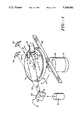
- FIG. 1 is a perspective view of a surface inspection apparatus of the present invention.
- FIG. 2 is a top plan view of the apparatus of FIG. 1.
- FIGS. 3 and 4 are side views of the apparatus of FIGS. 1 and 2 taken on respective lines 3--3 and 4--4 in FIG. 2.
- FIG. 5 is an enlarged side section of an inspection station for detecting surface roughness in the apparatus of FIG. 1.
- FIG. 6 is a schematic side view of the apparatus of FIG. 1 showing operation of a deformation detector.
- a wafer 11 is positioned on a rotating chuck 13.
- This chuck either uses a mechanical or electrostatic clampdown in a vacuum atmosphere, or alternatively, when at atmospheric pressure uses a vacuum holddown.
- the wafer 11 may be coated with dielectrics, such as silicon dioxide or BPSG, polysilicon, or metals such as aluminum or Al-Cu alloys, all giving it a surface with high background scatter.
- dielectrics such as silicon dioxide or BPSG, polysilicon, or metals such as aluminum or Al-Cu alloys, all giving it a surface with high background scatter.
- the wafer 11 While rotating about a spin axis 15 in a direction A, the wafer 11 is simultaneously translated in a direction B such that any fixed point 17 or 19 in effect describes a tightly wound spiral on the wafer 11.
- a starting position 11' of the wafer is shown in phantom in FIG. 2.
- the fixed illumination point 17 starts at the edge of wafer 11', and as the wafer moves under point 17, effectively spirals in toward the center C of the wafer.
- the fixed illumination point 19 starts at the center C of the wafer 11' and effectively spirals out to the edge as the wafer moves.
- a suitably positioned laser beam 21 or 23 will therefore sequentially illuminate all points on the wafer. Such systems are well known in the art of contamination inspection.
- the wafer 11 may be illuminated obliquely with a light beam 21.
- the beam 21 can be directed by a mirror 33 to a fixed point 17 so that the wafer 11 rotates and translates under it.
- the beam 21 has a relatively short wavelength.
- an argon ion laser 31 (488, 364 or 351 nm) could be used.
- the beam diameter may be on the order of 30 ⁇ m.
- Other light sources 31 such as He-Cd, frequency doubled diode lasers and frequency upconverted solid state lasers could also be selected.
- the incoming beam 21 is s-polarized.
- the direction of the propagation vector should intercept the axis of rotation 15 of the chuck 13 so that the rotation axis 15 is in the plane of incidence.
- the intersection 17 of the beam 21 with the plane of the wafer forms an elliptical spot with its major axis oriented in the radial direction B and its minor axis along the direction of wafer motion perpendicular to direction B.
- a is the beam diameter for an incoming circular beam
- the dimensions of the elongated spot in the plane of the wafer are respectively "a” and "a/sin ⁇ " where " ⁇ " is the angle of incidence.
- the angle of incidence ⁇ of the laser beam may vary, depending on the expected condition of the substrate, but typically will be between 5 and 20 degrees with respect to the plane of the wafer 11. For a 30 ⁇ m diameter beam incident on the wafer at an angle ⁇ of 15° above the wafer surface, the dimensions of the elliptical spot will be about 30 by 116 ⁇ m.
- the radial increment for each turn of the spiral must therefore be a small fraction of this dimension in order to have uniform detection sensitivity over the wafer 11, say one quarter of the above distance of 116 ⁇ m, i.e. 29 ⁇ m.
- a motor 41 with a spindle 43 rotates the chuck 13.
- An encoder 47 is provided with the motor 41 to provide position information ⁇ about the location of the particle.
- the scattered light 35 is picked up in a direction orthogonal to the illumination.
- a light collection system 39 is used that has a larger numerical aperture than would be the case for inspecting patterned wafers. This is possible, because, although these wafers have substantial roughness, scattering from them is less pronounced than from patterned wafers.
- a typical value for the elevation of the center of the receiving system is 25 degrees.
- optimum values depend on the expected conditions of the substrate.
- the numerical aperture of the receiving system 39 would typically be 0.5, corresponding to a half-angle of 30 degrees. Since the wafer 11 is simultaneously rotating and translating, both the illumination system 31 and 33 and the collection system 39 can be axially symmetrical and stationary, making them both very compact. The apparatus performs the particle detection on wafers exhibiting a great deal of surface roughness.
- the measurement of this roughness is also of considerable interest to the device manufacturer.
- One way to measure roughness is to measure the total integrated scatter (often referred to as TIS), which can then be correlated to the surface roughness in well known ways.
- TIS total integrated scatter
- the first inspection station 39 catches only a very small fraction of this scatter, as the primary design consideration is in fact elimination of this background.
- FIG. 5 illustrates a case where normal illumination and a Coblentz sphere 51 are utilized for light collection.
- a single or double parabolic collector may be used.
- the same laser 31 may or may not be used in this application.
- the mirror 33 may, for example, pivot in order to direct the beam along an alternate path 53 to a mirror 55.
- the mirror 55 would then reflect the beam 23 downward at approximately normal incidence through an aperture 57 in the Coblentz sphere 51.
- the two impact points 17 and 19 of the beams 21 and 23 may be positioned as illustrated in FIG. 2. In this case the rotation angle ⁇ is the same for both measurement points, and the radial displacement r is equal to the radius of the wafer.
- the Coblentz sphere configuration 51 corresponds to the one which is used in ASTM F1048-87 (although with a stationary sample) and therefore the results obtained can be directly expressed in terms of this standard.
- This setup can also be used for particles on smooth bare wafers as will now be described.
- the collection efficiency for light of a scattered particle in the case of the oblique incidence of the first collector system 39 illustrated in FIG. 1, is less than optimal. Its main purpose and advantage is that the scattering of the rough substrate is even more reduced. Therefore these systems are not as sensitive as the configurations used in normal incidence.
- diffusely scattered light 59 is directed from the inspection point 19 on the wafer 11 to a detector 61, via imaging off of the inner spherical mirror surface 60 of the Coblentz sphere 51.
- the specularly reflected light beam 62 exits the Coblentz sphere 51 through the same aperture 57 that the incident light beam 23 enters, and may be used for other measurements, such as of surface reflectance.
- the Coblentz sphere arrangement 51 provides for a very large collection angle of the scattered light 59, but the geometry does not provide for much background rejection. It is therefore also well suited for detection of particles on very smooth surfaces.
- a very small detector 61 such as a photo diode must typically be used as the available space is very restricted.
- a simple photo diode can be used, and the signal processing used can be fairly straightforward.
- a position sensitive detector 65 is placed in the path of the reflected oblique incident beam 67.
- the direction of the reflected beam 67 is a function of the local slope of the wafer.
- a change in the slope e of the substrate 11 will give rise to a change in the beam direction of 2e and a displacement of 2eR on the detector 65, where R is the distance from the point of impingement to the detector 65.
- R is the distance from the point of impingement to the detector 65. Knowing the local slope at each point 17, the surface profile itself can be reconstructed through integration.
- the wafer 11 may be held in a fixed angular position ⁇ o, and displaced along a radial direction B over a distance equal to the wafer radius, while the beam deflection signal 71 from the detector 65 is recorded.
- any of a variety of measurement methods could be used, using existing apparatus.
- the entire area of the wafer can be covered through rotation and translation.
- the main observation here is that the mechanics necessary for the rough film measurement can be advantageously combined with other measurement types, so that it is easy to obtain multiple capabilities in the same in-line instrument.
Abstract
Description
δ=3 [(1-ν)/E9 (t.sub.t /t.sub.s.sup.2) ρ.sup.2 σ
Claims (14)
Priority Applications (1)
| Application Number | Priority Date | Filing Date | Title |
|---|---|---|---|
| US07/736,517 US5189481A (en) | 1991-07-26 | 1991-07-26 | Particle detector for rough surfaces |
Applications Claiming Priority (1)
| Application Number | Priority Date | Filing Date | Title |
|---|---|---|---|
| US07/736,517 US5189481A (en) | 1991-07-26 | 1991-07-26 | Particle detector for rough surfaces |
Publications (1)
| Publication Number | Publication Date |
|---|---|
| US5189481A true US5189481A (en) | 1993-02-23 |
Family
ID=24960179
Family Applications (1)
| Application Number | Title | Priority Date | Filing Date |
|---|---|---|---|
| US07/736,517 Expired - Lifetime US5189481A (en) | 1991-07-26 | 1991-07-26 | Particle detector for rough surfaces |
Country Status (1)
| Country | Link |
|---|---|
| US (1) | US5189481A (en) |
Cited By (139)
| Publication number | Priority date | Publication date | Assignee | Title |
|---|---|---|---|---|
| US5319216A (en) * | 1991-07-26 | 1994-06-07 | Tokyo Electron Limited | Substrate detector with light emitting and receiving elements arranged in staggered fashion and a polarization filter |
| US5355212A (en) * | 1993-07-19 | 1994-10-11 | Tencor Instruments | Process for inspecting patterned wafers |
| US5389794A (en) * | 1992-11-25 | 1995-02-14 | Qc Optics, Inc. | Surface pit and mound detection and discrimination system and method |
| US5416594A (en) * | 1993-07-20 | 1995-05-16 | Tencor Instruments | Surface scanner with thin film gauge |
| WO1996027786A1 (en) * | 1995-03-06 | 1996-09-12 | Ade Optical Systems Corporation | Surface inspection system and method of inspecting surface of workpiece |
| US5608526A (en) * | 1995-01-19 | 1997-03-04 | Tencor Instruments | Focused beam spectroscopic ellipsometry method and system |
| US5631733A (en) * | 1995-01-20 | 1997-05-20 | Photon Dynamics, Inc. | Large area defect monitor tool for manufacture of clean surfaces |
| US5680215A (en) * | 1995-02-27 | 1997-10-21 | Lockheed Missiles & Space Company, Inc. | Vision inspection system and method |
| EP0804722A1 (en) * | 1994-12-08 | 1997-11-05 | Tencor Instruments | Surface inspection system |
| EP0804713A1 (en) * | 1994-12-21 | 1997-11-05 | Tencor Instruments | Optical wafer positioning system |
| WO1998037404A1 (en) * | 1997-02-21 | 1998-08-27 | Sidney Braginsky | Method of scanning semiconductor wafers to inspect for defects |
| US5801824A (en) * | 1996-11-25 | 1998-09-01 | Photon Dynamics, Inc. | Large area defect monitor tool for manufacture of clean surfaces |
| US5838445A (en) * | 1995-06-07 | 1998-11-17 | Micron Technology, Inc. | Method and apparatus for determining surface roughness |
| US5841662A (en) * | 1996-07-31 | 1998-11-24 | Coburn Optical Industries, Inc. | Method and apparatus for chucked work piece recognition |
| US5909276A (en) * | 1997-03-31 | 1999-06-01 | Microtherm, Llc | Optical inspection module and method for detecting particles and defects on substrates in integrated process tools |
| US5940175A (en) * | 1996-11-01 | 1999-08-17 | Msp Corporation | Method and apparatus for surface inspection in a chamber |
| WO2000023794A1 (en) * | 1998-10-16 | 2000-04-27 | Ade Optical Systems Corporation | Method and apparatus for mapping surface topography of a substrate |
| US6084671A (en) * | 1997-05-06 | 2000-07-04 | Holcomb; Matthew J. | Surface analysis using Gaussian beam profiles |
| US6118525A (en) * | 1995-03-06 | 2000-09-12 | Ade Optical Systems Corporation | Wafer inspection system for distinguishing pits and particles |
| WO2001013098A1 (en) * | 1999-08-16 | 2001-02-22 | Applied Materials, Inc. | Variable angle illumination wafer inspection system |
| US20010000977A1 (en) * | 1997-09-19 | 2001-05-10 | Mehdi Vaez-Iravani | Sample inspection system |
| US6271916B1 (en) | 1994-03-24 | 2001-08-07 | Kla-Tencor Corporation | Process and assembly for non-destructive surface inspections |
| US20020015146A1 (en) * | 1997-09-22 | 2002-02-07 | Meeks Steven W. | Combined high speed optical profilometer and ellipsometer |
| US20020097393A1 (en) * | 1994-12-08 | 2002-07-25 | Mehrdad Nikoonahad | Scanning system for inspecting anamolies on surfaces |
| US20020102749A1 (en) * | 2000-09-20 | 2002-08-01 | John Fielden | Methods and systems for determining a characteristic of a layer formed on a specimen by a deposition process |
| US20020106848A1 (en) * | 2000-09-20 | 2002-08-08 | Dan Wack | Methods and systems for determining a property of a specimen prior to, during, or subsequent to lithography |
| US20020107650A1 (en) * | 2000-09-20 | 2002-08-08 | Dan Wack | Methods and systems for determining a critical dimension and a presence of defects on a specimen |
| US20020145740A1 (en) * | 2001-03-26 | 2002-10-10 | Meeks Steven W. | Material independent optical profilometer |
| US20020163634A1 (en) * | 2001-03-26 | 2002-11-07 | Meeks Steven W. | Multiple spot size optical profilometer, ellipsometer, reflectometer and scatterometer |
| US6486946B1 (en) | 1999-06-15 | 2002-11-26 | Ade Corporation | Method for discriminating between holes in and particles on a film covering a substrate |
| US20020180961A1 (en) * | 2000-09-20 | 2002-12-05 | Dan Wack | Methods and systems for determining an adhesion characteristic and a thickness of a specimen |
| US20020186368A1 (en) * | 2001-06-08 | 2002-12-12 | Eliezer Rosengaus | Systems and methods for inspection of specimen surfaces |
| US20030025905A1 (en) * | 2001-03-26 | 2003-02-06 | Meeks Steven W. | Method of detecting and classifying scratches, particles and pits on thin film disks or wafers |
| US6538730B2 (en) | 2001-04-06 | 2003-03-25 | Kla-Tencor Technologies Corporation | Defect detection system |
| US6548821B1 (en) | 1999-06-21 | 2003-04-15 | Komag, Inc. | Method and apparatus for inspecting substrates |
| US6566674B1 (en) | 1999-06-21 | 2003-05-20 | Komag, Inc. | Method and apparatus for inspecting substrates |
| US20030139838A1 (en) * | 2002-01-16 | 2003-07-24 | Marella Paul Frank | Systems and methods for closed loop defect reduction |
| US6630996B2 (en) | 2000-11-15 | 2003-10-07 | Real Time Metrology, Inc. | Optical method and apparatus for inspecting large area planar objects |
| US20030197874A1 (en) * | 2002-04-19 | 2003-10-23 | Moghaddam Alireza Shahdoost | Method of detecting the thickness of thin film disks or wafers |
| US20030206294A1 (en) * | 1996-06-04 | 2003-11-06 | Leslie Brian C. | Optical scanning system for surface inspection |
| US20030230323A1 (en) * | 2002-06-14 | 2003-12-18 | Taiwan Semiconductor Manufacturing Co., Ltd. | Apparatus and method for improving scrubber cleaning |
| US6673637B2 (en) | 2000-09-20 | 2004-01-06 | Kla-Tencor Technologies | Methods and systems for determining a presence of macro defects and overlay of a specimen |
| US20040012775A1 (en) * | 2000-11-15 | 2004-01-22 | Kinney Patrick D. | Optical method and apparatus for inspecting large area planar objects |
| US20040017561A1 (en) * | 1997-09-22 | 2004-01-29 | Meeks Steven W. | Method of detecting and classifying scratches and particles on thin film disks or wafers |
| US6694284B1 (en) | 2000-09-20 | 2004-02-17 | Kla-Tencor Technologies Corp. | Methods and systems for determining at least four properties of a specimen |
| US20040032581A1 (en) * | 2002-01-15 | 2004-02-19 | Mehrdad Nikoonahad | Systems and methods for inspection of specimen surfaces |
| US20040046959A1 (en) * | 1997-09-22 | 2004-03-11 | Meeks Steven W. | System and method for simultaneously measuring thin film layer thickness, reflectivity, roughness, surface profile and magnetic pattern on thin film magnetic disks and silicon wafers |
| US20040057045A1 (en) * | 2000-12-21 | 2004-03-25 | Mehdi Vaez-Iravani | Sample inspection system |
| US6717671B1 (en) | 1997-09-22 | 2004-04-06 | Candela Instruments | System for simultaneously measuring thin film layer thickness, reflectivity, roughness, surface profile and magnetic pattern |
| US6734967B1 (en) * | 1995-01-19 | 2004-05-11 | Kla-Tencor Technologies Corporation | Focused beam spectroscopic ellipsometry method and system |
| US6757056B1 (en) | 2001-03-26 | 2004-06-29 | Candela Instruments | Combined high speed optical profilometer and ellipsometer |
| US20040125368A1 (en) * | 2002-09-13 | 2004-07-01 | Mehdi Vaez-Iravani | Inspection system for integrated applications |
| US20040156043A1 (en) * | 2003-01-09 | 2004-08-12 | Orbotech Ltd | Method and apparatus for simultaneous 2-D and topographical inspection |
| US20040169850A1 (en) * | 1999-07-02 | 2004-09-02 | Meeks Steven W. | System and method for double sided optical inspection of thin film disks or wafers |
| US6812045B1 (en) | 2000-09-20 | 2004-11-02 | Kla-Tencor, Inc. | Methods and systems for determining a characteristic of a specimen prior to, during, or subsequent to ion implantation |
| US20040235205A1 (en) * | 2000-09-20 | 2004-11-25 | Kla-Tencor, Inc. | Methods and systems for determining a critical dimension and overlay of a specimen |
| US20040263836A1 (en) * | 2003-06-30 | 2004-12-30 | Samsung Electronics Co., Ltd. | Method and apparatus for inspecting a wafer surface |
| US6853446B1 (en) | 1999-08-16 | 2005-02-08 | Applied Materials, Inc. | Variable angle illumination wafer inspection system |
| US20050036137A1 (en) * | 1994-12-08 | 2005-02-17 | Mehrdad Nikoonahad | Scanning system for inspecting anamolies on surfaces |
| US20050094136A1 (en) * | 2003-10-29 | 2005-05-05 | Xu James J. | Defect review system and method |
| US20050094864A1 (en) * | 2003-10-29 | 2005-05-05 | Xu James J. | Surface inspection system |
| US20050105791A1 (en) * | 2003-10-29 | 2005-05-19 | Lee Ken K. | Surface inspection method |
| US20050134841A1 (en) * | 1998-09-18 | 2005-06-23 | Mehdi Vacz-Iravani | Sample inspection system |
| US6919957B2 (en) | 2000-09-20 | 2005-07-19 | Kla-Tencor Technologies Corp. | Methods and systems for determining a critical dimension, a presence of defects, and a thin film characteristic of a specimen |
| US20050236569A1 (en) * | 2004-04-19 | 2005-10-27 | Kohei Yamaguchi | Scanning electron microscope |
| US20050259805A1 (en) * | 2000-10-30 | 2005-11-24 | Yoichi Okudera | Telephone directory assistane method and telephone directory assistance system |
| US20060007435A1 (en) * | 1997-09-19 | 2006-01-12 | Steve Biellak | Systems and methods for a wafer inspection system using multiple angles and multiple wavelength illumination |
| US20060062445A1 (en) * | 2004-09-14 | 2006-03-23 | Gaurav Verma | Methods, systems, and carrier media for evaluating reticle layout data |
| US7027143B1 (en) | 2002-10-15 | 2006-04-11 | Kla-Tencor Technologies Corp. | Methods and systems for inspecting reticles using aerial imaging at off-stepper wavelengths |
| US7075741B1 (en) | 2004-06-14 | 2006-07-11 | Kla Tencor Technologues Corporation | System and method for automatically determining magnetic eccentricity of a disk |
| US20060150841A1 (en) * | 2005-01-07 | 2006-07-13 | Heidelberger Druckmaschinen Ag | Printing press |
| US20060161452A1 (en) * | 2004-01-29 | 2006-07-20 | Kla-Tencor Technologies Corp. | Computer-implemented methods, processors, and systems for creating a wafer fabrication process |
| US7106425B1 (en) * | 2000-09-20 | 2006-09-12 | Kla-Tencor Technologies Corp. | Methods and systems for determining a presence of defects and a thin film characteristic of a specimen |
| US20060215289A1 (en) * | 2004-06-14 | 2006-09-28 | Kla-Tencor Technologies Corp. | Servo pattern characterization on magnetic disks |
| US7123356B1 (en) | 2002-10-15 | 2006-10-17 | Kla-Tencor Technologies Corp. | Methods and systems for inspecting reticles using aerial imaging and die-to-database detection |
| US7133119B1 (en) | 2002-12-17 | 2006-11-07 | Kla-Tencor Technologies Corp. | Systems for simulating high NA and polarization effects in aerial images |
| US20060250611A1 (en) * | 2005-05-06 | 2006-11-09 | Kla-Tencor Technologies Corp. | Wafer edge inspection |
| US20060250609A1 (en) * | 2005-05-06 | 2006-11-09 | Kla-Tencor Technologies Corp. | Wafer edge inspection |
| US20060250612A1 (en) * | 1997-09-22 | 2006-11-09 | Meeks Steven W | Detecting and classifying surface features or defects by controlling the angle of the illumination plane of incidence with respect to the feature or defect |
| US20060256345A1 (en) * | 2005-05-12 | 2006-11-16 | Kla-Tencor Technologies Corp. | Interferometry measurement in disturbed environments |
| US20060256325A1 (en) * | 2005-05-11 | 2006-11-16 | Kla-Tencor Technologies Corp. | Illumination energy management in surface inspection |
| US20060262291A1 (en) * | 2005-05-17 | 2006-11-23 | Hess Harald F | Dynamic reference plane compensation |
| US7201799B1 (en) | 2004-11-24 | 2007-04-10 | Kla-Tencor Technologies Corporation | System and method for classifying, detecting, and counting micropipes |
| US20070115483A1 (en) * | 1997-09-22 | 2007-05-24 | Oak Dave S | Surface finish roughness measurement |
| US20070156379A1 (en) * | 2005-11-18 | 2007-07-05 | Ashok Kulkarni | Methods and systems for utilizing design data in combination with inspection data |
| US20070230770A1 (en) * | 2005-11-18 | 2007-10-04 | Ashok Kulkarni | Methods and systems for determining a position of inspection data in design data space |
| US7286229B1 (en) | 2005-09-06 | 2007-10-23 | Kla-Tencor Technologies Corporation | Detecting multi-domain states in perpendicular magnetic media |
| US7295300B1 (en) | 2005-09-28 | 2007-11-13 | Kla-Tencor Technologies Corporation | Detecting surface pits |
| US20070262771A1 (en) * | 2006-05-11 | 2007-11-15 | Kla-Tencor Technologies Corporation | Method and System for Perpendicular Magnetic Media Metrology |
| US20070271064A1 (en) * | 2006-05-16 | 2007-11-22 | The Boeing Company | System and method for identifying a feature of a workpiece |
| US20070277919A1 (en) * | 2006-05-16 | 2007-12-06 | The Boeing Company | Systems and methods for monitoring automated composite manufacturing processes |
| US20070280501A1 (en) * | 2006-05-31 | 2007-12-06 | The Boeing Company | Method and System for Two-Dimensional and Three-Dimensional Inspection of a Workpiece |
| US20070288219A1 (en) * | 2005-11-18 | 2007-12-13 | Khurram Zafar | Methods and systems for utilizing design data in combination with inspection data |
| US7379175B1 (en) | 2002-10-15 | 2008-05-27 | Kla-Tencor Technologies Corp. | Methods and systems for reticle inspection and defect review using aerial imaging |
| US7397553B1 (en) | 2005-10-24 | 2008-07-08 | Kla-Tencor Technologies Corporation | Surface scanning |
| US7396022B1 (en) | 2004-09-28 | 2008-07-08 | Kla-Tencor Technologies Corp. | System and method for optimizing wafer flatness at high rotational speeds |
| US20080167829A1 (en) * | 2007-01-05 | 2008-07-10 | Allen Park | Methods and systems for using electrical information for a device being fabricated on a wafer to perform one or more defect-related functions |
| US20080180656A1 (en) * | 2007-01-26 | 2008-07-31 | Kla-Tencor Technologies Corporation | Surface characteristic analysis |
| US20090016595A1 (en) * | 2007-05-09 | 2009-01-15 | Peterson Ingrid B | Methods and systems for detecting defects in a reticle design pattern |
| US20090024967A1 (en) * | 2007-05-07 | 2009-01-22 | Bo Su | Computer-implemented methods, systems, and computer-readable media for determining a model for predicting printability of reticle features on a wafer |
| US20090043527A1 (en) * | 2007-08-10 | 2009-02-12 | Allen Park | Computer-implemented methods, carrier media, and systems for generating a metrology sampling plan |
| US20090041332A1 (en) * | 2007-07-20 | 2009-02-12 | Kla-Tencor Corporation | Methods for generating a standard reference die for use in a die to standard reference die inspection and methods for inspecting a wafer |
| US20090055783A1 (en) * | 2007-08-20 | 2009-02-26 | Kla-Tencor Corporation | Computer-implemented methods for determining if actual defects are potentially systematic defects or potentially random defects |
| US20090059236A1 (en) * | 2007-08-30 | 2009-03-05 | Kla-Tencor Technologies Corporation | Wafer Edge Inspection |
| US20090257645A1 (en) * | 2008-04-14 | 2009-10-15 | Chen Chien-Huei Adam | Methods and systems for determining a defect criticality index for defects on wafers |
| US7684032B1 (en) | 2005-01-06 | 2010-03-23 | Kla-Tencor Corporation | Multi-wavelength system and method for detecting epitaxial layer defects |
| US7714995B2 (en) | 1997-09-22 | 2010-05-11 | Kla-Tencor Corporation | Material independent profiler |
| US7738093B2 (en) | 2007-05-07 | 2010-06-15 | Kla-Tencor Corp. | Methods for detecting and classifying defects on a reticle |
| US7769225B2 (en) | 2005-08-02 | 2010-08-03 | Kla-Tencor Technologies Corp. | Methods and systems for detecting defects in a reticle design pattern |
| US20100235134A1 (en) * | 2009-03-13 | 2010-09-16 | Kla-Tencor Corporation | Methods and systems for generating an inspection process for a wafer |
| US7877722B2 (en) | 2006-12-19 | 2011-01-25 | Kla-Tencor Corp. | Systems and methods for creating inspection recipes |
| US20110187848A1 (en) * | 2008-07-28 | 2011-08-04 | Kla-Tencor Corporation | Computer-implemented methods, computer-readable media, and systems for classifying defects detected in a memory device area on a wafer |
| US20110194101A1 (en) * | 2008-10-15 | 2011-08-11 | Tachizaki Takehiro | Supersensitization of defect inspection method |
| US8204297B1 (en) | 2009-02-27 | 2012-06-19 | Kla-Tencor Corp. | Methods and systems for classifying defects detected on a reticle |
| WO2014039863A1 (en) * | 2012-09-09 | 2014-03-13 | Kla-Tencor Corporation | Monitoring incident beam position in a wafer inspection system |
| US8775101B2 (en) | 2009-02-13 | 2014-07-08 | Kla-Tencor Corp. | Detecting defects on a wafer |
| US8781781B2 (en) | 2010-07-30 | 2014-07-15 | Kla-Tencor Corp. | Dynamic care areas |
| US8826200B2 (en) | 2012-05-25 | 2014-09-02 | Kla-Tencor Corp. | Alteration for wafer inspection |
| US8831334B2 (en) | 2012-01-20 | 2014-09-09 | Kla-Tencor Corp. | Segmentation for wafer inspection |
| US8873596B2 (en) | 2011-07-22 | 2014-10-28 | Kla-Tencor Corporation | Laser with high quality, stable output beam, and long life high conversion efficiency non-linear crystal |
| US20150002835A1 (en) * | 2013-06-26 | 2015-01-01 | Taiwan Semiconductor Manufacturing Company., Ltd. | Wafer charging electromagnetic inspection tool and method of using |
| US20150090868A1 (en) * | 2012-04-23 | 2015-04-02 | Hitachi Maxell, Ltd. | Resin encoder scale, mold for resin encoder scale, method for producing resin encoder scale, and encoder |
| US9053527B2 (en) | 2013-01-02 | 2015-06-09 | Kla-Tencor Corp. | Detecting defects on a wafer |
| US9087367B2 (en) | 2011-09-13 | 2015-07-21 | Kla-Tencor Corp. | Determining design coordinates for wafer defects |
| US9092846B2 (en) | 2013-02-01 | 2015-07-28 | Kla-Tencor Corp. | Detecting defects on a wafer using defect-specific and multi-channel information |
| US9134254B2 (en) | 2013-01-07 | 2015-09-15 | Kla-Tencor Corp. | Determining a position of inspection system output in design data space |
| CN104931507A (en) * | 2015-06-05 | 2015-09-23 | 天津大学 | Mobile telephone shell edge quality detection system and mobile telephone shell edge quality detection method |
| US9151940B2 (en) | 2012-12-05 | 2015-10-06 | Kla-Tencor Corporation | Semiconductor inspection and metrology system using laser pulse multiplier |
| US9170211B2 (en) | 2011-03-25 | 2015-10-27 | Kla-Tencor Corp. | Design-based inspection using repeating structures |
| US9189844B2 (en) | 2012-10-15 | 2015-11-17 | Kla-Tencor Corp. | Detecting defects on a wafer using defect-specific information |
| US9250178B2 (en) | 2011-10-07 | 2016-02-02 | Kla-Tencor Corporation | Passivation of nonlinear optical crystals |
| US9310320B2 (en) | 2013-04-15 | 2016-04-12 | Kla-Tencor Corp. | Based sampling and binning for yield critical defects |
| US9311698B2 (en) | 2013-01-09 | 2016-04-12 | Kla-Tencor Corp. | Detecting defects on a wafer using template image matching |
| US9419407B2 (en) | 2014-09-25 | 2016-08-16 | Kla-Tencor Corporation | Laser assembly and inspection system using monolithic bandwidth narrowing apparatus |
| US9448184B1 (en) | 2012-01-09 | 2016-09-20 | Kla-Tencor Corporation | Method and system for determining one or more optical characteristics of structure of a semiconductor wafer |
| US9525265B2 (en) | 2014-06-20 | 2016-12-20 | Kla-Tencor Corporation | Laser repetition rate multiplier and flat-top beam profile generators using mirrors and/or prisms |
| US9793673B2 (en) | 2011-06-13 | 2017-10-17 | Kla-Tencor Corporation | Semiconductor inspection and metrology system using laser pulse multiplier |
| US9804101B2 (en) | 2014-03-20 | 2017-10-31 | Kla-Tencor Corporation | System and method for reducing the bandwidth of a laser and an inspection system and method using a laser |
| US9865512B2 (en) | 2013-04-08 | 2018-01-09 | Kla-Tencor Corp. | Dynamic design attributes for wafer inspection |
Citations (6)
| Publication number | Priority date | Publication date | Assignee | Title |
|---|---|---|---|---|
| US3857637A (en) * | 1973-01-10 | 1974-12-31 | Ppg Industries Inc | Surface distortion analyzer |
| US4069484A (en) * | 1976-05-28 | 1978-01-17 | Rca Corporation | Defect plotting system |
| US4614427A (en) * | 1983-05-20 | 1986-09-30 | Hitachi, Ltd. | Automatic contaminants detection apparatus |
| JPS6367549A (en) * | 1986-09-10 | 1988-03-26 | Pioneer Electronic Corp | Defect inspecting and film thickness measuring instrument for resist original disk |
| US4740708A (en) * | 1987-01-06 | 1988-04-26 | International Business Machines Corporation | Semiconductor wafer surface inspection apparatus and method |
| US4902131A (en) * | 1985-03-28 | 1990-02-20 | Kabushiki Kaisha Toshiba | Surface inspection method and apparatus therefor |
-
1991
- 1991-07-26 US US07/736,517 patent/US5189481A/en not_active Expired - Lifetime
Patent Citations (6)
| Publication number | Priority date | Publication date | Assignee | Title |
|---|---|---|---|---|
| US3857637A (en) * | 1973-01-10 | 1974-12-31 | Ppg Industries Inc | Surface distortion analyzer |
| US4069484A (en) * | 1976-05-28 | 1978-01-17 | Rca Corporation | Defect plotting system |
| US4614427A (en) * | 1983-05-20 | 1986-09-30 | Hitachi, Ltd. | Automatic contaminants detection apparatus |
| US4902131A (en) * | 1985-03-28 | 1990-02-20 | Kabushiki Kaisha Toshiba | Surface inspection method and apparatus therefor |
| JPS6367549A (en) * | 1986-09-10 | 1988-03-26 | Pioneer Electronic Corp | Defect inspecting and film thickness measuring instrument for resist original disk |
| US4740708A (en) * | 1987-01-06 | 1988-04-26 | International Business Machines Corporation | Semiconductor wafer surface inspection apparatus and method |
Non-Patent Citations (4)
| Title |
|---|
| R. Browning et al., "Recent advances in automated patterned wafer inspection," SPIE Proceedings, vol. 1087, pp. 440-445 (1989). |
| R. Browning et al., Recent advances in automated patterned wafer inspection, SPIE Proceedings , vol. 1087, pp. 440 445 (1989). * |
| Tencor Instruments, Surfscan 7000 Patterned Wafer Contamination Analyzer , (product brochure), Mar. 1990. * |
| Tencor Instruments, Surfscan 7000 Patterned Wafer Contamination Analyzer, (product brochure), Mar. 19909. |
Cited By (278)
| Publication number | Priority date | Publication date | Assignee | Title |
|---|---|---|---|---|
| US5319216A (en) * | 1991-07-26 | 1994-06-07 | Tokyo Electron Limited | Substrate detector with light emitting and receiving elements arranged in staggered fashion and a polarization filter |
| US5389794A (en) * | 1992-11-25 | 1995-02-14 | Qc Optics, Inc. | Surface pit and mound detection and discrimination system and method |
| US5355212A (en) * | 1993-07-19 | 1994-10-11 | Tencor Instruments | Process for inspecting patterned wafers |
| US5416594A (en) * | 1993-07-20 | 1995-05-16 | Tencor Instruments | Surface scanner with thin film gauge |
| US20070103676A1 (en) * | 1994-03-24 | 2007-05-10 | Kla-Tencor Corporation | Process and Assembly for Non-Destructive Surface Inspections |
| US7102744B2 (en) | 1994-03-24 | 2006-09-05 | Kla-Tencor Corporation | Process and assembly for non-destructive surface inspections |
| US7477371B2 (en) | 1994-03-24 | 2009-01-13 | Kla-Tencor Corporation | Process and assembly for non-destructive surface inspections |
| US6606153B2 (en) | 1994-03-24 | 2003-08-12 | Kla-Tencor Corporation | Process and assembly for non-destructive surface inspections |
| US20040080741A1 (en) * | 1994-03-24 | 2004-04-29 | Norbert Marxer | Process and assembly for non-destructive surface inspections |
| US6271916B1 (en) | 1994-03-24 | 2001-08-07 | Kla-Tencor Corporation | Process and assembly for non-destructive surface inspections |
| EP0804722A1 (en) * | 1994-12-08 | 1997-11-05 | Tencor Instruments | Surface inspection system |
| US20050036137A1 (en) * | 1994-12-08 | 2005-02-17 | Mehrdad Nikoonahad | Scanning system for inspecting anamolies on surfaces |
| US20020097393A1 (en) * | 1994-12-08 | 2002-07-25 | Mehrdad Nikoonahad | Scanning system for inspecting anamolies on surfaces |
| US6636302B2 (en) | 1994-12-08 | 2003-10-21 | Kla-Tencor Corporation | Scanning system for inspecting anamolies on surfaces |
| EP0804722A4 (en) * | 1994-12-08 | 1999-03-24 | Tencor Instruments | Surface inspection system |
| US20050110986A1 (en) * | 1994-12-08 | 2005-05-26 | Mehrdad Nikoonahad | Scanning system for inspecting anamolies on surfaces |
| US7084967B2 (en) | 1994-12-08 | 2006-08-01 | KLA —Tencor Corporation | Scanning system for inspecting anomalies on surfaces |
| EP0804713A1 (en) * | 1994-12-21 | 1997-11-05 | Tencor Instruments | Optical wafer positioning system |
| EP0804713A4 (en) * | 1994-12-21 | 1999-03-24 | Tencor Instruments | Optical wafer positioning system |
| US5910842A (en) * | 1995-01-19 | 1999-06-08 | Kla-Tencor Corporation | Focused beam spectroscopic ellipsometry method and system |
| US20050105090A1 (en) * | 1995-01-19 | 2005-05-19 | Piwonka-Corle Timothy R. | Focused beam spectroscopic ellipsometry method and system |
| US20040100632A1 (en) * | 1995-01-19 | 2004-05-27 | Piwonka-Corle Timothy R. | Focused beam spectroscopic ellipsometry method and system |
| US5608526A (en) * | 1995-01-19 | 1997-03-04 | Tencor Instruments | Focused beam spectroscopic ellipsometry method and system |
| US6734967B1 (en) * | 1995-01-19 | 2004-05-11 | Kla-Tencor Technologies Corporation | Focused beam spectroscopic ellipsometry method and system |
| US5631733A (en) * | 1995-01-20 | 1997-05-20 | Photon Dynamics, Inc. | Large area defect monitor tool for manufacture of clean surfaces |
| US5680215A (en) * | 1995-02-27 | 1997-10-21 | Lockheed Missiles & Space Company, Inc. | Vision inspection system and method |
| US5712701A (en) * | 1995-03-06 | 1998-01-27 | Ade Optical Systems Corporation | Surface inspection system and method of inspecting surface of workpiece |
| US6118525A (en) * | 1995-03-06 | 2000-09-12 | Ade Optical Systems Corporation | Wafer inspection system for distinguishing pits and particles |
| WO1996027786A1 (en) * | 1995-03-06 | 1996-09-12 | Ade Optical Systems Corporation | Surface inspection system and method of inspecting surface of workpiece |
| US6509965B2 (en) | 1995-03-06 | 2003-01-21 | Ade Optical Systems Corporation | Wafer inspection system for distinguishing pits and particles |
| US6292259B1 (en) | 1995-03-06 | 2001-09-18 | Ade Optical Systems Corporation | Wafer inspection system for distinguishing pits and particles |
| US5838445A (en) * | 1995-06-07 | 1998-11-17 | Micron Technology, Inc. | Method and apparatus for determining surface roughness |
| US7477372B2 (en) | 1996-06-04 | 2009-01-13 | Kla-Tencor Technologies Corporation | Optical scanning system for surface inspection |
| US6888627B2 (en) | 1996-06-04 | 2005-05-03 | Kla-Tencor Corporation | Optical scanning system for surface inspection |
| US20030206294A1 (en) * | 1996-06-04 | 2003-11-06 | Leslie Brian C. | Optical scanning system for surface inspection |
| US7075637B2 (en) | 1996-06-04 | 2006-07-11 | Kla-Tencor Corporation | Optical scanning system for surface inspection |
| US20070188744A1 (en) * | 1996-06-04 | 2007-08-16 | Kla-Tencor Technologies Corporation | Optical Scanning System For Surface Inspection |
| US20030227619A1 (en) * | 1996-06-04 | 2003-12-11 | Leslie Brian C. | Optical scanning system for surface inspection |
| US5841662A (en) * | 1996-07-31 | 1998-11-24 | Coburn Optical Industries, Inc. | Method and apparatus for chucked work piece recognition |
| US5940175A (en) * | 1996-11-01 | 1999-08-17 | Msp Corporation | Method and apparatus for surface inspection in a chamber |
| US5801824A (en) * | 1996-11-25 | 1998-09-01 | Photon Dynamics, Inc. | Large area defect monitor tool for manufacture of clean surfaces |
| WO1998037404A1 (en) * | 1997-02-21 | 1998-08-27 | Sidney Braginsky | Method of scanning semiconductor wafers to inspect for defects |
| US5909276A (en) * | 1997-03-31 | 1999-06-01 | Microtherm, Llc | Optical inspection module and method for detecting particles and defects on substrates in integrated process tools |
| US6084671A (en) * | 1997-05-06 | 2000-07-04 | Holcomb; Matthew J. | Surface analysis using Gaussian beam profiles |
| US20050099621A1 (en) * | 1997-09-19 | 2005-05-12 | Mehdi Vaez-Iravani | Sample inspection system |
| US6891611B1 (en) | 1997-09-19 | 2005-05-10 | Kla- Tencor Corporation | Sample inspection system |
| US7218392B2 (en) | 1997-09-19 | 2007-05-15 | Kla-Tencor Technologies Corporation | Systems and methods for a wafer inspection system using multiple angles and multiple wavelength illumination |
| US7064821B2 (en) | 1997-09-19 | 2006-06-20 | Kla-Tencor Technologies Corporation | Sample inspection system |
| US7079238B2 (en) | 1997-09-19 | 2006-07-18 | Kla-Tencor Technologies Corporation | Sample inspection system |
| US20060007435A1 (en) * | 1997-09-19 | 2006-01-12 | Steve Biellak | Systems and methods for a wafer inspection system using multiple angles and multiple wavelength illumination |
| US7119897B2 (en) | 1997-09-19 | 2006-10-10 | Kla-Tencor Technologies Corporation | Sample inspection system |
| US6618134B2 (en) | 1997-09-19 | 2003-09-09 | Kla-Tencor Corporation | Sample inspection system |
| US20010000977A1 (en) * | 1997-09-19 | 2001-05-10 | Mehdi Vaez-Iravani | Sample inspection system |
| US6657715B2 (en) | 1997-09-19 | 2003-12-02 | Kla-Tencor Corporation | Sample inspection system |
| US20050174568A1 (en) * | 1997-09-19 | 2005-08-11 | Mehdi Vaez-Iravani | Sample inspection system |
| US6384910B2 (en) * | 1997-09-19 | 2002-05-07 | Kla-Tencor Corporation | Sample inspection system |
| US6639662B2 (en) | 1997-09-19 | 2003-10-28 | Kla-Tencor Corporation | Sample inspection system |
| US7714995B2 (en) | 1997-09-22 | 2010-05-11 | Kla-Tencor Corporation | Material independent profiler |
| US20020015146A1 (en) * | 1997-09-22 | 2002-02-07 | Meeks Steven W. | Combined high speed optical profilometer and ellipsometer |
| US6956660B2 (en) | 1997-09-22 | 2005-10-18 | Kla-Tencor Technologies | System and method for measuring properties of an object using a phase difference between two reflected light signals |
| US7123357B2 (en) | 1997-09-22 | 2006-10-17 | Candela Instruments | Method of detecting and classifying scratches and particles on thin film disks or wafers |
| US20060250612A1 (en) * | 1997-09-22 | 2006-11-09 | Meeks Steven W | Detecting and classifying surface features or defects by controlling the angle of the illumination plane of incidence with respect to the feature or defect |
| US6717671B1 (en) | 1997-09-22 | 2004-04-06 | Candela Instruments | System for simultaneously measuring thin film layer thickness, reflectivity, roughness, surface profile and magnetic pattern |
| US7630086B2 (en) | 1997-09-22 | 2009-12-08 | Kla-Tencor Corporation | Surface finish roughness measurement |
| US20040017561A1 (en) * | 1997-09-22 | 2004-01-29 | Meeks Steven W. | Method of detecting and classifying scratches and particles on thin film disks or wafers |
| US20070115483A1 (en) * | 1997-09-22 | 2007-05-24 | Oak Dave S | Surface finish roughness measurement |
| US6956658B2 (en) | 1997-09-22 | 2005-10-18 | Kla-Tencor Technologies Corporation | System and method for measuring object characteristics using phase differences in polarized light reflections |
| US20040046959A1 (en) * | 1997-09-22 | 2004-03-11 | Meeks Steven W. | System and method for simultaneously measuring thin film layer thickness, reflectivity, roughness, surface profile and magnetic pattern on thin film magnetic disks and silicon wafers |
| US7688435B2 (en) * | 1997-09-22 | 2010-03-30 | Kla-Tencor Corporation | Detecting and classifying surface features or defects by controlling the angle of the illumination plane of incidence with respect to the feature or defect |
| US20050134841A1 (en) * | 1998-09-18 | 2005-06-23 | Mehdi Vacz-Iravani | Sample inspection system |
| WO2000023794A1 (en) * | 1998-10-16 | 2000-04-27 | Ade Optical Systems Corporation | Method and apparatus for mapping surface topography of a substrate |
| US6621581B1 (en) | 1998-10-16 | 2003-09-16 | Ade Corporation | Method and apparatus for mapping surface topography of a substrate |
| US6486946B1 (en) | 1999-06-15 | 2002-11-26 | Ade Corporation | Method for discriminating between holes in and particles on a film covering a substrate |
| US6566674B1 (en) | 1999-06-21 | 2003-05-20 | Komag, Inc. | Method and apparatus for inspecting substrates |
| US6548821B1 (en) | 1999-06-21 | 2003-04-15 | Komag, Inc. | Method and apparatus for inspecting substrates |
| US7061601B2 (en) | 1999-07-02 | 2006-06-13 | Kla-Tencor Technologies Corporation | System and method for double sided optical inspection of thin film disks or wafers |
| US20040169850A1 (en) * | 1999-07-02 | 2004-09-02 | Meeks Steven W. | System and method for double sided optical inspection of thin film disks or wafers |
| WO2001013098A1 (en) * | 1999-08-16 | 2001-02-22 | Applied Materials, Inc. | Variable angle illumination wafer inspection system |
| US6853446B1 (en) | 1999-08-16 | 2005-02-08 | Applied Materials, Inc. | Variable angle illumination wafer inspection system |
| US20020179864A1 (en) * | 2000-09-20 | 2002-12-05 | John Fielden | Methods and systems for determining a thin film characteristic and an electrical property of a specimen |
| US6946394B2 (en) * | 2000-09-20 | 2005-09-20 | Kla-Tencor Technologies | Methods and systems for determining a characteristic of a layer formed on a specimen by a deposition process |
| US8179530B2 (en) | 2000-09-20 | 2012-05-15 | Kla-Tencor Technologies Corp. | Methods and systems for determining a critical dimension and overlay of a specimen |
| US6806951B2 (en) | 2000-09-20 | 2004-10-19 | Kla-Tencor Technologies Corp. | Methods and systems for determining at least one characteristic of defects on at least two sides of a specimen |
| US7139083B2 (en) * | 2000-09-20 | 2006-11-21 | Kla-Tencor Technologies Corp. | Methods and systems for determining a composition and a thickness of a specimen |
| US6812045B1 (en) | 2000-09-20 | 2004-11-02 | Kla-Tencor, Inc. | Methods and systems for determining a characteristic of a specimen prior to, during, or subsequent to ion implantation |
| US6818459B2 (en) | 2000-09-20 | 2004-11-16 | Kla-Tencor Technologies Corp. | Methods and systems for determining a presence of macro defects and overlay of a specimen |
| US7130029B2 (en) * | 2000-09-20 | 2006-10-31 | Kla-Tencor Technologies Corp. | Methods and systems for determining an adhesion characteristic and a thickness of a specimen |
| US20040235205A1 (en) * | 2000-09-20 | 2004-11-25 | Kla-Tencor, Inc. | Methods and systems for determining a critical dimension and overlay of a specimen |
| US6829559B2 (en) | 2000-09-20 | 2004-12-07 | K.L.A.-Tencor Technologies | Methods and systems for determining a presence of macro and micro defects on a specimen |
| US7751046B2 (en) | 2000-09-20 | 2010-07-06 | Kla-Tencor Technologies Corp. | Methods and systems for determining a critical dimension and overlay of a specimen |
| US7196782B2 (en) * | 2000-09-20 | 2007-03-27 | Kla-Tencor Technologies Corp. | Methods and systems for determining a thin film characteristic and an electrical property of a specimen |
| US8502979B2 (en) | 2000-09-20 | 2013-08-06 | Kla-Tencor Technologies Corp. | Methods and systems for determining a critical dimension and overlay of a specimen |
| US20020102749A1 (en) * | 2000-09-20 | 2002-08-01 | John Fielden | Methods and systems for determining a characteristic of a layer formed on a specimen by a deposition process |
| US20020103564A1 (en) * | 2000-09-20 | 2002-08-01 | John Fielden | Methods and systems for determining a composition and a thickness of a specimen |
| US20020106848A1 (en) * | 2000-09-20 | 2002-08-08 | Dan Wack | Methods and systems for determining a property of a specimen prior to, during, or subsequent to lithography |
| US20020107650A1 (en) * | 2000-09-20 | 2002-08-08 | Dan Wack | Methods and systems for determining a critical dimension and a presence of defects on a specimen |
| US20040115843A1 (en) * | 2000-09-20 | 2004-06-17 | Kla-Tencor, Inc. | Methods and systems for determining a presence of macro defects and overlay of a specimen |
| US20040092045A1 (en) * | 2000-09-20 | 2004-05-13 | Gary Bultman | Methods and systems for determining a presence of macro and micro defects on a specimen |
| US20040073398A1 (en) * | 2000-09-20 | 2004-04-15 | Kla-Tencor, Inc. | Methods and systems for determining a critical dimension and a thin film characteristic of a specimen |
| US6891627B1 (en) | 2000-09-20 | 2005-05-10 | Kla-Tencor Technologies Corp. | Methods and systems for determining a critical dimension and overlay of a specimen |
| US6891610B2 (en) | 2000-09-20 | 2005-05-10 | Kla-Tencor Technologies Corp. | Methods and systems for determining an implant characteristic and a presence of defects on a specimen |
| US7106425B1 (en) * | 2000-09-20 | 2006-09-12 | Kla-Tencor Technologies Corp. | Methods and systems for determining a presence of defects and a thin film characteristic of a specimen |
| US20020179867A1 (en) * | 2000-09-20 | 2002-12-05 | John Fielden | Methods and systems for determining flatness, a presence of defects, and a thin film characteristic of a specimen |
| US6694284B1 (en) | 2000-09-20 | 2004-02-17 | Kla-Tencor Technologies Corp. | Methods and systems for determining at least four properties of a specimen |
| US20020180961A1 (en) * | 2000-09-20 | 2002-12-05 | Dan Wack | Methods and systems for determining an adhesion characteristic and a thickness of a specimen |
| US20020188417A1 (en) * | 2000-09-20 | 2002-12-12 | Ady Levy | Methods and systems for determining a property of a specimen prior to, during, or subsequent to an etch process |
| US6673637B2 (en) | 2000-09-20 | 2004-01-06 | Kla-Tencor Technologies | Methods and systems for determining a presence of macro defects and overlay of a specimen |
| US20020190207A1 (en) * | 2000-09-20 | 2002-12-19 | Ady Levy | Methods and systems for determining a characteristic of micro defects on a specimen |
| US7349090B2 (en) * | 2000-09-20 | 2008-03-25 | Kla-Tencor Technologies Corp. | Methods and systems for determining a property of a specimen prior to, during, or subsequent to lithography |
| US6917419B2 (en) | 2000-09-20 | 2005-07-12 | Kla-Tencor Technologies Corp. | Methods and systems for determining flatness, a presence of defects, and a thin film characteristic of a specimen |
| US6917433B2 (en) * | 2000-09-20 | 2005-07-12 | Kla-Tencor Technologies Corp. | Methods and systems for determining a property of a specimen prior to, during, or subsequent to an etch process |
| US6919957B2 (en) | 2000-09-20 | 2005-07-19 | Kla-Tencor Technologies Corp. | Methods and systems for determining a critical dimension, a presence of defects, and a thin film characteristic of a specimen |
| US20030011786A1 (en) * | 2000-09-20 | 2003-01-16 | Ady Levy | Methods and systems for determining overlay and flatness of a specimen |
| US6782337B2 (en) | 2000-09-20 | 2004-08-24 | Kla-Tencor Technologies Corp. | Methods and systems for determining a critical dimension an a presence of defects on a specimen |
| US6950196B2 (en) | 2000-09-20 | 2005-09-27 | Kla-Tencor Technologies Corp. | Methods and systems for determining a thickness of a structure on a specimen and at least one additional property of the specimen |
| US7460981B2 (en) | 2000-09-20 | 2008-12-02 | Kla-Tencor Technologies Corp. | Methods and systems for determining a presence of macro and micro defects on a specimen |
| US6633831B2 (en) | 2000-09-20 | 2003-10-14 | Kla Tencor Technologies | Methods and systems for determining a critical dimension and a thin film characteristic of a specimen |
| US20060072807A1 (en) * | 2000-09-20 | 2006-04-06 | Kla-Tencor Technologies. | Methods and systems for determining a presence of macro and micro defects on a specimen |
| US7006235B2 (en) | 2000-09-20 | 2006-02-28 | Kla-Tencor Technologies Corp. | Methods and systems for determining overlay and flatness of a specimen |
| US20050259805A1 (en) * | 2000-10-30 | 2005-11-24 | Yoichi Okudera | Telephone directory assistane method and telephone directory assistance system |
| US20040012775A1 (en) * | 2000-11-15 | 2004-01-22 | Kinney Patrick D. | Optical method and apparatus for inspecting large area planar objects |
| US6809809B2 (en) | 2000-11-15 | 2004-10-26 | Real Time Metrology, Inc. | Optical method and apparatus for inspecting large area planar objects |
| US6630996B2 (en) | 2000-11-15 | 2003-10-07 | Real Time Metrology, Inc. | Optical method and apparatus for inspecting large area planar objects |
| US20040057045A1 (en) * | 2000-12-21 | 2004-03-25 | Mehdi Vaez-Iravani | Sample inspection system |
| US7113284B1 (en) | 2001-03-26 | 2006-09-26 | Kla-Tencor Technologies Corporation | Material independent optical profilometer |
| US6897957B2 (en) | 2001-03-26 | 2005-05-24 | Candela Instruments | Material independent optical profilometer |
| US20050057747A1 (en) * | 2001-03-26 | 2005-03-17 | Meeks Steven W. | Method of detecting and classifying scratches, particles and pits on thin film disks or wafers |
| US20040233419A1 (en) * | 2001-03-26 | 2004-11-25 | Meeks Steven W. | Combined high speed optical profilometer and ellipsometer |
| US7075630B2 (en) | 2001-03-26 | 2006-07-11 | Kla-Tencor Technologies Corporation | Combined high speed optical profilometer and ellipsometer |
| US6909500B2 (en) | 2001-03-26 | 2005-06-21 | Candela Instruments | Method of detecting and classifying scratches, particles and pits on thin film disks or wafers |
| US20020163634A1 (en) * | 2001-03-26 | 2002-11-07 | Meeks Steven W. | Multiple spot size optical profilometer, ellipsometer, reflectometer and scatterometer |
| US20020145740A1 (en) * | 2001-03-26 | 2002-10-10 | Meeks Steven W. | Material independent optical profilometer |
| US6757056B1 (en) | 2001-03-26 | 2004-06-29 | Candela Instruments | Combined high speed optical profilometer and ellipsometer |
| US20030025905A1 (en) * | 2001-03-26 | 2003-02-06 | Meeks Steven W. | Method of detecting and classifying scratches, particles and pits on thin film disks or wafers |
| US20050018181A1 (en) * | 2001-04-06 | 2005-01-27 | Mehdi Vaez-Iravani | Defect detection system |
| US6862096B2 (en) | 2001-04-06 | 2005-03-01 | Kla-Tencor Corporation | Defect detection system |
| US20030210393A1 (en) * | 2001-04-06 | 2003-11-13 | Kla-Tencor Corporation | Defect detection system |
| US6538730B2 (en) | 2001-04-06 | 2003-03-25 | Kla-Tencor Technologies Corporation | Defect detection system |
| US20020186368A1 (en) * | 2001-06-08 | 2002-12-12 | Eliezer Rosengaus | Systems and methods for inspection of specimen surfaces |
| US7072034B2 (en) | 2001-06-08 | 2006-07-04 | Kla-Tencor Corporation | Systems and methods for inspection of specimen surfaces |
| US20040032581A1 (en) * | 2002-01-15 | 2004-02-19 | Mehrdad Nikoonahad | Systems and methods for inspection of specimen surfaces |
| US20030139838A1 (en) * | 2002-01-16 | 2003-07-24 | Marella Paul Frank | Systems and methods for closed loop defect reduction |
| US7236847B2 (en) | 2002-01-16 | 2007-06-26 | Kla-Tencor Technologies Corp. | Systems and methods for closed loop defect reduction |
| US6882437B2 (en) | 2002-04-19 | 2005-04-19 | Kla-Tencor Technologies | Method of detecting the thickness of thin film disks or wafers |
| US20030197874A1 (en) * | 2002-04-19 | 2003-10-23 | Moghaddam Alireza Shahdoost | Method of detecting the thickness of thin film disks or wafers |
| US20030230323A1 (en) * | 2002-06-14 | 2003-12-18 | Taiwan Semiconductor Manufacturing Co., Ltd. | Apparatus and method for improving scrubber cleaning |
| US7116413B2 (en) | 2002-09-13 | 2006-10-03 | Kla-Tencor Corporation | Inspection system for integrated applications |
| US20040125368A1 (en) * | 2002-09-13 | 2004-07-01 | Mehdi Vaez-Iravani | Inspection system for integrated applications |
| US7123356B1 (en) | 2002-10-15 | 2006-10-17 | Kla-Tencor Technologies Corp. | Methods and systems for inspecting reticles using aerial imaging and die-to-database detection |
| US7027143B1 (en) | 2002-10-15 | 2006-04-11 | Kla-Tencor Technologies Corp. | Methods and systems for inspecting reticles using aerial imaging at off-stepper wavelengths |
| US7379175B1 (en) | 2002-10-15 | 2008-05-27 | Kla-Tencor Technologies Corp. | Methods and systems for reticle inspection and defect review using aerial imaging |
| US7133119B1 (en) | 2002-12-17 | 2006-11-07 | Kla-Tencor Technologies Corp. | Systems for simulating high NA and polarization effects in aerial images |
| US20040156043A1 (en) * | 2003-01-09 | 2004-08-12 | Orbotech Ltd | Method and apparatus for simultaneous 2-D and topographical inspection |
| US7253891B2 (en) * | 2003-01-09 | 2007-08-07 | Orbotech Ltd. | Method and apparatus for simultaneous 2-D and topographical inspection |
| US20040263836A1 (en) * | 2003-06-30 | 2004-12-30 | Samsung Electronics Co., Ltd. | Method and apparatus for inspecting a wafer surface |
| US7310140B2 (en) * | 2003-06-30 | 2007-12-18 | Samsung Electronics Co., Ltd. | Method and apparatus for inspecting a wafer surface |
| US20050105791A1 (en) * | 2003-10-29 | 2005-05-19 | Lee Ken K. | Surface inspection method |
| US7110106B2 (en) | 2003-10-29 | 2006-09-19 | Coretech Optical, Inc. | Surface inspection system |
| US20050094136A1 (en) * | 2003-10-29 | 2005-05-05 | Xu James J. | Defect review system and method |
| US7433031B2 (en) | 2003-10-29 | 2008-10-07 | Core Tech Optical, Inc. | Defect review system with 2D scanning and a ring detector |
| US20050094864A1 (en) * | 2003-10-29 | 2005-05-05 | Xu James J. | Surface inspection system |
| US20060161452A1 (en) * | 2004-01-29 | 2006-07-20 | Kla-Tencor Technologies Corp. | Computer-implemented methods, processors, and systems for creating a wafer fabrication process |
| US20060236294A1 (en) * | 2004-01-29 | 2006-10-19 | Saidin Zain K | Computer-implemented methods for detecting defects in reticle design data |
| US7646906B2 (en) | 2004-01-29 | 2010-01-12 | Kla-Tencor Technologies Corp. | Computer-implemented methods for detecting defects in reticle design data |
| US20050236569A1 (en) * | 2004-04-19 | 2005-10-27 | Kohei Yamaguchi | Scanning electron microscope |
| US7307254B2 (en) * | 2004-04-19 | 2007-12-11 | Hitachi High-Technologies Corporation | Scanning electron microscope |
| US20060215289A1 (en) * | 2004-06-14 | 2006-09-28 | Kla-Tencor Technologies Corp. | Servo pattern characterization on magnetic disks |
| US7075741B1 (en) | 2004-06-14 | 2006-07-11 | Kla Tencor Technologues Corporation | System and method for automatically determining magnetic eccentricity of a disk |
| US7397621B2 (en) | 2004-06-14 | 2008-07-08 | Kla-Tencor Technologies Corporation | Servo pattern characterization on magnetic disks |
| US7689966B2 (en) | 2004-09-14 | 2010-03-30 | Kla-Tencor Technologies Corp. | Methods, systems, and carrier media for evaluating reticle layout data |
| US20060062445A1 (en) * | 2004-09-14 | 2006-03-23 | Gaurav Verma | Methods, systems, and carrier media for evaluating reticle layout data |
| US7396022B1 (en) | 2004-09-28 | 2008-07-08 | Kla-Tencor Technologies Corp. | System and method for optimizing wafer flatness at high rotational speeds |
| US7201799B1 (en) | 2004-11-24 | 2007-04-10 | Kla-Tencor Technologies Corporation | System and method for classifying, detecting, and counting micropipes |
| US7684032B1 (en) | 2005-01-06 | 2010-03-23 | Kla-Tencor Corporation | Multi-wavelength system and method for detecting epitaxial layer defects |
| US20060150841A1 (en) * | 2005-01-07 | 2006-07-13 | Heidelberger Druckmaschinen Ag | Printing press |
| US7161669B2 (en) | 2005-05-06 | 2007-01-09 | Kla- Tencor Technologies Corporation | Wafer edge inspection |
| US20060250611A1 (en) * | 2005-05-06 | 2006-11-09 | Kla-Tencor Technologies Corp. | Wafer edge inspection |
| US7532318B2 (en) | 2005-05-06 | 2009-05-12 | Kla-Tencor Corporation | Wafer edge inspection |
| US20070127016A1 (en) * | 2005-05-06 | 2007-06-07 | Meeks Steven W | Wafer edge inspection |
| US20060250610A1 (en) * | 2005-05-06 | 2006-11-09 | Kla-Tencor Technologies Corp. | Wafer edge inspection |
| US7161667B2 (en) | 2005-05-06 | 2007-01-09 | Kla-Tencor Technologies Corporation | Wafer edge inspection |
| US20060250609A1 (en) * | 2005-05-06 | 2006-11-09 | Kla-Tencor Technologies Corp. | Wafer edge inspection |
| US7161668B2 (en) | 2005-05-06 | 2007-01-09 | Kla-Tencor Technologies Corporation | Wafer edge inspection |
| US20060256325A1 (en) * | 2005-05-11 | 2006-11-16 | Kla-Tencor Technologies Corp. | Illumination energy management in surface inspection |
| US7548308B2 (en) | 2005-05-11 | 2009-06-16 | Kla-Tencor Corporation | Illumination energy management in surface inspection |
| US20060256345A1 (en) * | 2005-05-12 | 2006-11-16 | Kla-Tencor Technologies Corp. | Interferometry measurement in disturbed environments |
| US7505143B2 (en) | 2005-05-17 | 2009-03-17 | Kla-Tencor Corporation | Dynamic reference plane compensation |
| US20060262291A1 (en) * | 2005-05-17 | 2006-11-23 | Hess Harald F | Dynamic reference plane compensation |
| US7769225B2 (en) | 2005-08-02 | 2010-08-03 | Kla-Tencor Technologies Corp. | Methods and systems for detecting defects in a reticle design pattern |
| US7286229B1 (en) | 2005-09-06 | 2007-10-23 | Kla-Tencor Technologies Corporation | Detecting multi-domain states in perpendicular magnetic media |
| US7295300B1 (en) | 2005-09-28 | 2007-11-13 | Kla-Tencor Technologies Corporation | Detecting surface pits |
| US7397553B1 (en) | 2005-10-24 | 2008-07-08 | Kla-Tencor Technologies Corporation | Surface scanning |
| US20100119144A1 (en) * | 2005-11-18 | 2010-05-13 | Kla-Tencor Technologies Corporation | Methods and systems for utilizing design data in combination with inspection data |
| US7676077B2 (en) | 2005-11-18 | 2010-03-09 | Kla-Tencor Technologies Corp. | Methods and systems for utilizing design data in combination with inspection data |
| US8923600B2 (en) | 2005-11-18 | 2014-12-30 | Kla-Tencor Technologies Corp. | Methods and systems for utilizing design data in combination with inspection data |
| US20070156379A1 (en) * | 2005-11-18 | 2007-07-05 | Ashok Kulkarni | Methods and systems for utilizing design data in combination with inspection data |
| US8041103B2 (en) | 2005-11-18 | 2011-10-18 | Kla-Tencor Technologies Corp. | Methods and systems for determining a position of inspection data in design data space |
| US20070288219A1 (en) * | 2005-11-18 | 2007-12-13 | Khurram Zafar | Methods and systems for utilizing design data in combination with inspection data |
| US7570796B2 (en) | 2005-11-18 | 2009-08-04 | Kla-Tencor Technologies Corp. | Methods and systems for utilizing design data in combination with inspection data |
| US20090297019A1 (en) * | 2005-11-18 | 2009-12-03 | Kla-Tencor Technologies Corporation | Methods and systems for utilizing design data in combination with inspection data |
| US20070230770A1 (en) * | 2005-11-18 | 2007-10-04 | Ashok Kulkarni | Methods and systems for determining a position of inspection data in design data space |
| US8139843B2 (en) | 2005-11-18 | 2012-03-20 | Kla-Tencor Technologies Corp. | Methods and systems for utilizing design data in combination with inspection data |
| US20070262771A1 (en) * | 2006-05-11 | 2007-11-15 | Kla-Tencor Technologies Corporation | Method and System for Perpendicular Magnetic Media Metrology |
| US7684145B2 (en) | 2006-05-11 | 2010-03-23 | Microsense, Llc | Method and system for perpendicular magnetic media metrology |
| US20100002326A1 (en) * | 2006-05-11 | 2010-01-07 | Ade Technologies, Inc. | Method and system for perpendicular magnetic media metrology |
| US8050486B2 (en) | 2006-05-16 | 2011-11-01 | The Boeing Company | System and method for identifying a feature of a workpiece |
| US20070271064A1 (en) * | 2006-05-16 | 2007-11-22 | The Boeing Company | System and method for identifying a feature of a workpiece |
| US20070277919A1 (en) * | 2006-05-16 | 2007-12-06 | The Boeing Company | Systems and methods for monitoring automated composite manufacturing processes |
| EP1857260B1 (en) | 2006-05-16 | 2015-09-16 | The Boeing Company | Systems and methods for monitoring automated composite fabrication processes |
| US20070280501A1 (en) * | 2006-05-31 | 2007-12-06 | The Boeing Company | Method and System for Two-Dimensional and Three-Dimensional Inspection of a Workpiece |
| US9052294B2 (en) | 2006-05-31 | 2015-06-09 | The Boeing Company | Method and system for two-dimensional and three-dimensional inspection of a workpiece |
| US7877722B2 (en) | 2006-12-19 | 2011-01-25 | Kla-Tencor Corp. | Systems and methods for creating inspection recipes |
| US20080167829A1 (en) * | 2007-01-05 | 2008-07-10 | Allen Park | Methods and systems for using electrical information for a device being fabricated on a wafer to perform one or more defect-related functions |
| US8194968B2 (en) | 2007-01-05 | 2012-06-05 | Kla-Tencor Corp. | Methods and systems for using electrical information for a device being fabricated on a wafer to perform one or more defect-related functions |
| US20080180656A1 (en) * | 2007-01-26 | 2008-07-31 | Kla-Tencor Technologies Corporation | Surface characteristic analysis |
| US7554654B2 (en) | 2007-01-26 | 2009-06-30 | Kla-Tencor Corporation | Surface characteristic analysis |
| US7738093B2 (en) | 2007-05-07 | 2010-06-15 | Kla-Tencor Corp. | Methods for detecting and classifying defects on a reticle |
| US20090024967A1 (en) * | 2007-05-07 | 2009-01-22 | Bo Su | Computer-implemented methods, systems, and computer-readable media for determining a model for predicting printability of reticle features on a wafer |
| US7962863B2 (en) | 2007-05-07 | 2011-06-14 | Kla-Tencor Corp. | Computer-implemented methods, systems, and computer-readable media for determining a model for predicting printability of reticle features on a wafer |
| US20090016595A1 (en) * | 2007-05-09 | 2009-01-15 | Peterson Ingrid B | Methods and systems for detecting defects in a reticle design pattern |
| US8213704B2 (en) | 2007-05-09 | 2012-07-03 | Kla-Tencor Corp. | Methods and systems for detecting defects in a reticle design pattern |
| US20090041332A1 (en) * | 2007-07-20 | 2009-02-12 | Kla-Tencor Corporation | Methods for generating a standard reference die for use in a die to standard reference die inspection and methods for inspecting a wafer |
| US7796804B2 (en) | 2007-07-20 | 2010-09-14 | Kla-Tencor Corp. | Methods for generating a standard reference die for use in a die to standard reference die inspection and methods for inspecting a wafer |
| US20100329540A1 (en) * | 2007-07-20 | 2010-12-30 | Kla-Tencor Corporation | Methods for generating a standard reference die for use in a die to standard reference die inspection and methods for inspecting a wafer |
| US8204296B2 (en) | 2007-07-20 | 2012-06-19 | Kla-Tencor Corp. | Methods for generating a standard reference die for use in a die to standard reference die inspection and methods for inspecting a wafer |
| US20090043527A1 (en) * | 2007-08-10 | 2009-02-12 | Allen Park | Computer-implemented methods, carrier media, and systems for generating a metrology sampling plan |
| US7711514B2 (en) | 2007-08-10 | 2010-05-04 | Kla-Tencor Technologies Corp. | Computer-implemented methods, carrier media, and systems for generating a metrology sampling plan |
| US7975245B2 (en) | 2007-08-20 | 2011-07-05 | Kla-Tencor Corp. | Computer-implemented methods for determining if actual defects are potentially systematic defects or potentially random defects |
| US20090055783A1 (en) * | 2007-08-20 | 2009-02-26 | Kla-Tencor Corporation | Computer-implemented methods for determining if actual defects are potentially systematic defects or potentially random defects |
| US7656519B2 (en) | 2007-08-30 | 2010-02-02 | Kla-Tencor Corporation | Wafer edge inspection |
| US20090059236A1 (en) * | 2007-08-30 | 2009-03-05 | Kla-Tencor Technologies Corporation | Wafer Edge Inspection |
| US8139844B2 (en) | 2008-04-14 | 2012-03-20 | Kla-Tencor Corp. | Methods and systems for determining a defect criticality index for defects on wafers |
| US20090257645A1 (en) * | 2008-04-14 | 2009-10-15 | Chen Chien-Huei Adam | Methods and systems for determining a defect criticality index for defects on wafers |
| US9659670B2 (en) | 2008-07-28 | 2017-05-23 | Kla-Tencor Corp. | Computer-implemented methods, computer-readable media, and systems for classifying defects detected in a memory device area on a wafer |
| US20110187848A1 (en) * | 2008-07-28 | 2011-08-04 | Kla-Tencor Corporation | Computer-implemented methods, computer-readable media, and systems for classifying defects detected in a memory device area on a wafer |
| US20110194101A1 (en) * | 2008-10-15 | 2011-08-11 | Tachizaki Takehiro | Supersensitization of defect inspection method |
| US8775101B2 (en) | 2009-02-13 | 2014-07-08 | Kla-Tencor Corp. | Detecting defects on a wafer |
| US8204297B1 (en) | 2009-02-27 | 2012-06-19 | Kla-Tencor Corp. | Methods and systems for classifying defects detected on a reticle |
| US20100235134A1 (en) * | 2009-03-13 | 2010-09-16 | Kla-Tencor Corporation | Methods and systems for generating an inspection process for a wafer |
| US8112241B2 (en) | 2009-03-13 | 2012-02-07 | Kla-Tencor Corp. | Methods and systems for generating an inspection process for a wafer |
| US8781781B2 (en) | 2010-07-30 | 2014-07-15 | Kla-Tencor Corp. | Dynamic care areas |
| US9170211B2 (en) | 2011-03-25 | 2015-10-27 | Kla-Tencor Corp. | Design-based inspection using repeating structures |
| US10193293B2 (en) | 2011-06-13 | 2019-01-29 | Kla-Tencor Corporation | Semiconductor inspection and metrology system using laser pulse multiplier |
| US9972959B2 (en) | 2011-06-13 | 2018-05-15 | Kla-Tencor Corporation | Semiconductor inspection and metrology system using laser pulse multiplier |
| US9793673B2 (en) | 2011-06-13 | 2017-10-17 | Kla-Tencor Corporation | Semiconductor inspection and metrology system using laser pulse multiplier |
| US9097683B2 (en) | 2011-07-22 | 2015-08-04 | Kla-Tencor Corporation | Laser with high quality, stable output beam, and long life high conversion efficiency non-linear crystal |
| US8873596B2 (en) | 2011-07-22 | 2014-10-28 | Kla-Tencor Corporation | Laser with high quality, stable output beam, and long life high conversion efficiency non-linear crystal |
| US9413134B2 (en) | 2011-07-22 | 2016-08-09 | Kla-Tencor Corporation | Multi-stage ramp-up annealing for frequency-conversion crystals |
| US9087367B2 (en) | 2011-09-13 | 2015-07-21 | Kla-Tencor Corp. | Determining design coordinates for wafer defects |
| US9459215B2 (en) | 2011-10-07 | 2016-10-04 | Kla-Tencor Corporation | Passivation of nonlinear optical crystals |
| US11227770B2 (en) | 2011-10-07 | 2022-01-18 | Kla Corporation | Passivation of nonlinear optical crystals |
| US10283366B2 (en) | 2011-10-07 | 2019-05-07 | Kla-Tencor Corporation | Passivation of nonlinear optical crystals |
| US9250178B2 (en) | 2011-10-07 | 2016-02-02 | Kla-Tencor Corporation | Passivation of nonlinear optical crystals |
| US9448184B1 (en) | 2012-01-09 | 2016-09-20 | Kla-Tencor Corporation | Method and system for determining one or more optical characteristics of structure of a semiconductor wafer |
| US8831334B2 (en) | 2012-01-20 | 2014-09-09 | Kla-Tencor Corp. | Segmentation for wafer inspection |
| US10288453B2 (en) * | 2012-04-23 | 2019-05-14 | Maxell, Ltd. | Resin encoder scale, mold for resin encoder scale, method for producing resin encoder scale, and encoder |
| US20150090868A1 (en) * | 2012-04-23 | 2015-04-02 | Hitachi Maxell, Ltd. | Resin encoder scale, mold for resin encoder scale, method for producing resin encoder scale, and encoder |
| US8826200B2 (en) | 2012-05-25 | 2014-09-02 | Kla-Tencor Corp. | Alteration for wafer inspection |
| US8934091B2 (en) | 2012-09-09 | 2015-01-13 | Kla-Tencor Corp. | Monitoring incident beam position in a wafer inspection system |
| WO2014039863A1 (en) * | 2012-09-09 | 2014-03-13 | Kla-Tencor Corporation | Monitoring incident beam position in a wafer inspection system |
| US9189844B2 (en) | 2012-10-15 | 2015-11-17 | Kla-Tencor Corp. | Detecting defects on a wafer using defect-specific information |
| US9151940B2 (en) | 2012-12-05 | 2015-10-06 | Kla-Tencor Corporation | Semiconductor inspection and metrology system using laser pulse multiplier |
| US9768577B2 (en) | 2012-12-05 | 2017-09-19 | Kla-Tencor Corporation | Semiconductor inspection and metrology system using laser pulse multiplier |
| US9053527B2 (en) | 2013-01-02 | 2015-06-09 | Kla-Tencor Corp. | Detecting defects on a wafer |
| US9134254B2 (en) | 2013-01-07 | 2015-09-15 | Kla-Tencor Corp. | Determining a position of inspection system output in design data space |
| US9311698B2 (en) | 2013-01-09 | 2016-04-12 | Kla-Tencor Corp. | Detecting defects on a wafer using template image matching |
| US9092846B2 (en) | 2013-02-01 | 2015-07-28 | Kla-Tencor Corp. | Detecting defects on a wafer using defect-specific and multi-channel information |
| US9865512B2 (en) | 2013-04-08 | 2018-01-09 | Kla-Tencor Corp. | Dynamic design attributes for wafer inspection |
| US9310320B2 (en) | 2013-04-15 | 2016-04-12 | Kla-Tencor Corp. | Based sampling and binning for yield critical defects |
| US9423359B2 (en) * | 2013-06-26 | 2016-08-23 | Taiwan Semiconductor Manufacturing Company, Ltd. | Wafer charging electromagnetic inspection tool and method of using |
| US20150002835A1 (en) * | 2013-06-26 | 2015-01-01 | Taiwan Semiconductor Manufacturing Company., Ltd. | Wafer charging electromagnetic inspection tool and method of using |
| US9804101B2 (en) | 2014-03-20 | 2017-10-31 | Kla-Tencor Corporation | System and method for reducing the bandwidth of a laser and an inspection system and method using a laser |
| US10495582B2 (en) | 2014-03-20 | 2019-12-03 | Kla-Tencor Corporation | System and method for reducing the bandwidth of a laser and an inspection system and method using a laser |
| US10044164B2 (en) | 2014-06-20 | 2018-08-07 | Kla-Tencor Corporation | Laser repetition rate multiplier and flat-top beam profile generators using mirrors and/or prisms |
| US9525265B2 (en) | 2014-06-20 | 2016-12-20 | Kla-Tencor Corporation | Laser repetition rate multiplier and flat-top beam profile generators using mirrors and/or prisms |
| US9419407B2 (en) | 2014-09-25 | 2016-08-16 | Kla-Tencor Corporation | Laser assembly and inspection system using monolithic bandwidth narrowing apparatus |
| CN104931507B (en) * | 2015-06-05 | 2017-11-21 | 天津大学 | A kind of phone housing edge quality detecting system and detection method |
| CN104931507A (en) * | 2015-06-05 | 2015-09-23 | 天津大学 | Mobile telephone shell edge quality detection system and mobile telephone shell edge quality detection method |
Similar Documents
| Publication | Publication Date | Title |
|---|---|---|
| US5189481A (en) | Particle detector for rough surfaces | |
| US7433034B1 (en) | Darkfield defect inspection with spectral contents | |
| JP3801635B2 (en) | Product surface inspection system and method | |
| US7477371B2 (en) | Process and assembly for non-destructive surface inspections | |
| US7271921B2 (en) | Method and apparatus for determining surface layer thickness using continuous multi-wavelength surface scanning | |
| US7362425B2 (en) | Wide spatial frequency topography and roughness measurement | |
| US6538730B2 (en) | Defect detection system | |
| EP1553406B1 (en) | Method for double sided optical inspection of thin film disks | |
| US6721052B2 (en) | Systems for measuring periodic structures | |
| JP5438064B2 (en) | Inspection system improved for integrated use | |
| US20070229833A1 (en) | High-sensitivity surface detection system and method | |
| US7123357B2 (en) | Method of detecting and classifying scratches and particles on thin film disks or wafers | |
| JP5425494B2 (en) | Improvement of defect detection system | |
| US20030025905A1 (en) | Method of detecting and classifying scratches, particles and pits on thin film disks or wafers | |
| US20060072126A1 (en) | Material independent optical profilometer | |
| JP3432273B2 (en) | Foreign matter inspection device and foreign matter inspection method | |
| US5936254A (en) | Thin film detection method and apparatus | |
| WO1999032879A1 (en) | Method and apparatus for reducing roughness scatter as a noise source in wafer scanning systems |
Legal Events
| Date | Code | Title | Description |
|---|---|---|---|
| AS | Assignment |
Owner name: TENCOR INSTRUMENTS A CORP. OF CA, CALIFORNIA Free format text: ASSIGNMENT OF ASSIGNORS INTEREST.;ASSIGNORS:JANN, PETER C.;GROSS, KENNETH P.;NEUKERMANS, ARMAND P.;REEL/FRAME:005803/0559 Effective date: 19910724 |
|
| STCF | Information on status: patent grant |
Free format text: PATENTED CASE |
|
| CC | Certificate of correction | ||
| FEPP | Fee payment procedure |
Free format text: PAT HLDR NO LONGER CLAIMS SMALL ENT STAT AS SMALL BUSINESS (ORIGINAL EVENT CODE: LSM2); ENTITY STATUS OF PATENT OWNER: LARGE ENTITY Free format text: PAYOR NUMBER ASSIGNED (ORIGINAL EVENT CODE: ASPN); ENTITY STATUS OF PATENT OWNER: LARGE ENTITY |
|
| FPAY | Fee payment |
Year of fee payment: 4 |
|
| FPAY | Fee payment |
Year of fee payment: 8 |
|
| FEPP | Fee payment procedure |
Free format text: PAYER NUMBER DE-ASSIGNED (ORIGINAL EVENT CODE: RMPN); ENTITY STATUS OF PATENT OWNER: LARGE ENTITY Free format text: PAYOR NUMBER ASSIGNED (ORIGINAL EVENT CODE: ASPN); ENTITY STATUS OF PATENT OWNER: LARGE ENTITY |
|
| FPAY | Fee payment |
Year of fee payment: 12 |