US5182632A - High density multichip package with interconnect structure and heatsink - Google Patents
High density multichip package with interconnect structure and heatsink Download PDFInfo
- Publication number
- US5182632A US5182632A US07/804,614 US80461491A US5182632A US 5182632 A US5182632 A US 5182632A US 80461491 A US80461491 A US 80461491A US 5182632 A US5182632 A US 5182632A
- Authority
- US
- United States
- Prior art keywords
- chips
- package
- pads
- chip
- interconnect
- Prior art date
- Legal status (The legal status is an assumption and is not a legal conclusion. Google has not performed a legal analysis and makes no representation as to the accuracy of the status listed.)
- Expired - Fee Related
Links
Images


Classifications
-
- H—ELECTRICITY
- H01—ELECTRIC ELEMENTS
- H01L—SEMICONDUCTOR DEVICES NOT COVERED BY CLASS H10
- H01L24/00—Arrangements for connecting or disconnecting semiconductor or solid-state bodies; Methods or apparatus related thereto
- H01L24/01—Means for bonding being attached to, or being formed on, the surface to be connected, e.g. chip-to-package, die-attach, "first-level" interconnects; Manufacturing methods related thereto
- H01L24/26—Layer connectors, e.g. plate connectors, solder or adhesive layers; Manufacturing methods related thereto
- H01L24/31—Structure, shape, material or disposition of the layer connectors after the connecting process
- H01L24/32—Structure, shape, material or disposition of the layer connectors after the connecting process of an individual layer connector
-
- H—ELECTRICITY
- H01—ELECTRIC ELEMENTS
- H01L—SEMICONDUCTOR DEVICES NOT COVERED BY CLASS H10
- H01L23/00—Details of semiconductor or other solid state devices
- H01L23/34—Arrangements for cooling, heating, ventilating or temperature compensation ; Temperature sensing arrangements
- H01L23/36—Selection of materials, or shaping, to facilitate cooling or heating, e.g. heatsinks
- H01L23/367—Cooling facilitated by shape of device
- H01L23/3675—Cooling facilitated by shape of device characterised by the shape of the housing
-
- H—ELECTRICITY
- H01—ELECTRIC ELEMENTS
- H01L—SEMICONDUCTOR DEVICES NOT COVERED BY CLASS H10
- H01L23/00—Details of semiconductor or other solid state devices
- H01L23/52—Arrangements for conducting electric current within the device in operation from one component to another, i.e. interconnections, e.g. wires, lead frames
- H01L23/538—Arrangements for conducting electric current within the device in operation from one component to another, i.e. interconnections, e.g. wires, lead frames the interconnection structure between a plurality of semiconductor chips being formed on, or in, insulating substrates
-
- H—ELECTRICITY
- H01—ELECTRIC ELEMENTS
- H01L—SEMICONDUCTOR DEVICES NOT COVERED BY CLASS H10
- H01L23/00—Details of semiconductor or other solid state devices
- H01L23/58—Structural electrical arrangements for semiconductor devices not otherwise provided for, e.g. in combination with batteries
- H01L23/64—Impedance arrangements
- H01L23/642—Capacitive arrangements
-
- H—ELECTRICITY
- H01—ELECTRIC ELEMENTS
- H01L—SEMICONDUCTOR DEVICES NOT COVERED BY CLASS H10
- H01L23/00—Details of semiconductor or other solid state devices
- H01L23/58—Structural electrical arrangements for semiconductor devices not otherwise provided for, e.g. in combination with batteries
- H01L23/64—Impedance arrangements
- H01L23/647—Resistive arrangements
-
- H—ELECTRICITY
- H01—ELECTRIC ELEMENTS
- H01L—SEMICONDUCTOR DEVICES NOT COVERED BY CLASS H10
- H01L24/00—Arrangements for connecting or disconnecting semiconductor or solid-state bodies; Methods or apparatus related thereto
- H01L24/01—Means for bonding being attached to, or being formed on, the surface to be connected, e.g. chip-to-package, die-attach, "first-level" interconnects; Manufacturing methods related thereto
- H01L24/26—Layer connectors, e.g. plate connectors, solder or adhesive layers; Manufacturing methods related thereto
- H01L24/28—Structure, shape, material or disposition of the layer connectors prior to the connecting process
- H01L24/29—Structure, shape, material or disposition of the layer connectors prior to the connecting process of an individual layer connector
-
- H—ELECTRICITY
- H01—ELECTRIC ELEMENTS
- H01L—SEMICONDUCTOR DEVICES NOT COVERED BY CLASS H10
- H01L24/00—Arrangements for connecting or disconnecting semiconductor or solid-state bodies; Methods or apparatus related thereto
- H01L24/01—Means for bonding being attached to, or being formed on, the surface to be connected, e.g. chip-to-package, die-attach, "first-level" interconnects; Manufacturing methods related thereto
- H01L24/42—Wire connectors; Manufacturing methods related thereto
- H01L24/47—Structure, shape, material or disposition of the wire connectors after the connecting process
- H01L24/48—Structure, shape, material or disposition of the wire connectors after the connecting process of an individual wire connector
-
- H—ELECTRICITY
- H01—ELECTRIC ELEMENTS
- H01L—SEMICONDUCTOR DEVICES NOT COVERED BY CLASS H10
- H01L25/00—Assemblies consisting of a plurality of individual semiconductor or other solid state devices ; Multistep manufacturing processes thereof
- H01L25/03—Assemblies consisting of a plurality of individual semiconductor or other solid state devices ; Multistep manufacturing processes thereof all the devices being of a type provided for in the same subgroup of groups H01L27/00 - H01L33/00, or in a single subclass of H10K, H10N, e.g. assemblies of rectifier diodes
- H01L25/04—Assemblies consisting of a plurality of individual semiconductor or other solid state devices ; Multistep manufacturing processes thereof all the devices being of a type provided for in the same subgroup of groups H01L27/00 - H01L33/00, or in a single subclass of H10K, H10N, e.g. assemblies of rectifier diodes the devices not having separate containers
- H01L25/065—Assemblies consisting of a plurality of individual semiconductor or other solid state devices ; Multistep manufacturing processes thereof all the devices being of a type provided for in the same subgroup of groups H01L27/00 - H01L33/00, or in a single subclass of H10K, H10N, e.g. assemblies of rectifier diodes the devices not having separate containers the devices being of a type provided for in group H01L27/00
- H01L25/0652—Assemblies consisting of a plurality of individual semiconductor or other solid state devices ; Multistep manufacturing processes thereof all the devices being of a type provided for in the same subgroup of groups H01L27/00 - H01L33/00, or in a single subclass of H10K, H10N, e.g. assemblies of rectifier diodes the devices not having separate containers the devices being of a type provided for in group H01L27/00 the devices being arranged next and on each other, i.e. mixed assemblies
-
- H—ELECTRICITY
- H01—ELECTRIC ELEMENTS
- H01L—SEMICONDUCTOR DEVICES NOT COVERED BY CLASS H10
- H01L2224/00—Indexing scheme for arrangements for connecting or disconnecting semiconductor or solid-state bodies and methods related thereto as covered by H01L24/00
- H01L2224/01—Means for bonding being attached to, or being formed on, the surface to be connected, e.g. chip-to-package, die-attach, "first-level" interconnects; Manufacturing methods related thereto
- H01L2224/02—Bonding areas; Manufacturing methods related thereto
- H01L2224/04—Structure, shape, material or disposition of the bonding areas prior to the connecting process
- H01L2224/0401—Bonding areas specifically adapted for bump connectors, e.g. under bump metallisation [UBM]
-
- H—ELECTRICITY
- H01—ELECTRIC ELEMENTS
- H01L—SEMICONDUCTOR DEVICES NOT COVERED BY CLASS H10
- H01L2224/00—Indexing scheme for arrangements for connecting or disconnecting semiconductor or solid-state bodies and methods related thereto as covered by H01L24/00
- H01L2224/01—Means for bonding being attached to, or being formed on, the surface to be connected, e.g. chip-to-package, die-attach, "first-level" interconnects; Manufacturing methods related thereto
- H01L2224/10—Bump connectors; Manufacturing methods related thereto
- H01L2224/15—Structure, shape, material or disposition of the bump connectors after the connecting process
- H01L2224/16—Structure, shape, material or disposition of the bump connectors after the connecting process of an individual bump connector
- H01L2224/161—Disposition
- H01L2224/16151—Disposition the bump connector connecting between a semiconductor or solid-state body and an item not being a semiconductor or solid-state body, e.g. chip-to-substrate, chip-to-passive
- H01L2224/16221—Disposition the bump connector connecting between a semiconductor or solid-state body and an item not being a semiconductor or solid-state body, e.g. chip-to-substrate, chip-to-passive the body and the item being stacked
- H01L2224/16225—Disposition the bump connector connecting between a semiconductor or solid-state body and an item not being a semiconductor or solid-state body, e.g. chip-to-substrate, chip-to-passive the body and the item being stacked the item being non-metallic, e.g. insulating substrate with or without metallisation
-
- H—ELECTRICITY
- H01—ELECTRIC ELEMENTS
- H01L—SEMICONDUCTOR DEVICES NOT COVERED BY CLASS H10
- H01L2224/00—Indexing scheme for arrangements for connecting or disconnecting semiconductor or solid-state bodies and methods related thereto as covered by H01L24/00
- H01L2224/01—Means for bonding being attached to, or being formed on, the surface to be connected, e.g. chip-to-package, die-attach, "first-level" interconnects; Manufacturing methods related thereto
- H01L2224/26—Layer connectors, e.g. plate connectors, solder or adhesive layers; Manufacturing methods related thereto
- H01L2224/2612—Auxiliary members for layer connectors, e.g. spacers
-
- H—ELECTRICITY
- H01—ELECTRIC ELEMENTS
- H01L—SEMICONDUCTOR DEVICES NOT COVERED BY CLASS H10
- H01L2224/00—Indexing scheme for arrangements for connecting or disconnecting semiconductor or solid-state bodies and methods related thereto as covered by H01L24/00
- H01L2224/01—Means for bonding being attached to, or being formed on, the surface to be connected, e.g. chip-to-package, die-attach, "first-level" interconnects; Manufacturing methods related thereto
- H01L2224/26—Layer connectors, e.g. plate connectors, solder or adhesive layers; Manufacturing methods related thereto
- H01L2224/31—Structure, shape, material or disposition of the layer connectors after the connecting process
- H01L2224/32—Structure, shape, material or disposition of the layer connectors after the connecting process of an individual layer connector
- H01L2224/321—Disposition
- H01L2224/32151—Disposition the layer connector connecting between a semiconductor or solid-state body and an item not being a semiconductor or solid-state body, e.g. chip-to-substrate, chip-to-passive
- H01L2224/32221—Disposition the layer connector connecting between a semiconductor or solid-state body and an item not being a semiconductor or solid-state body, e.g. chip-to-substrate, chip-to-passive the body and the item being stacked
- H01L2224/32225—Disposition the layer connector connecting between a semiconductor or solid-state body and an item not being a semiconductor or solid-state body, e.g. chip-to-substrate, chip-to-passive the body and the item being stacked the item being non-metallic, e.g. insulating substrate with or without metallisation
-
- H—ELECTRICITY
- H01—ELECTRIC ELEMENTS
- H01L—SEMICONDUCTOR DEVICES NOT COVERED BY CLASS H10
- H01L2224/00—Indexing scheme for arrangements for connecting or disconnecting semiconductor or solid-state bodies and methods related thereto as covered by H01L24/00
- H01L2224/01—Means for bonding being attached to, or being formed on, the surface to be connected, e.g. chip-to-package, die-attach, "first-level" interconnects; Manufacturing methods related thereto
- H01L2224/42—Wire connectors; Manufacturing methods related thereto
- H01L2224/47—Structure, shape, material or disposition of the wire connectors after the connecting process
- H01L2224/48—Structure, shape, material or disposition of the wire connectors after the connecting process of an individual wire connector
- H01L2224/4805—Shape
- H01L2224/4809—Loop shape
- H01L2224/48091—Arched
-
- H—ELECTRICITY
- H01—ELECTRIC ELEMENTS
- H01L—SEMICONDUCTOR DEVICES NOT COVERED BY CLASS H10
- H01L2224/00—Indexing scheme for arrangements for connecting or disconnecting semiconductor or solid-state bodies and methods related thereto as covered by H01L24/00
- H01L2224/01—Means for bonding being attached to, or being formed on, the surface to be connected, e.g. chip-to-package, die-attach, "first-level" interconnects; Manufacturing methods related thereto
- H01L2224/42—Wire connectors; Manufacturing methods related thereto
- H01L2224/47—Structure, shape, material or disposition of the wire connectors after the connecting process
- H01L2224/48—Structure, shape, material or disposition of the wire connectors after the connecting process of an individual wire connector
- H01L2224/481—Disposition
- H01L2224/48151—Connecting between a semiconductor or solid-state body and an item not being a semiconductor or solid-state body, e.g. chip-to-substrate, chip-to-passive
- H01L2224/48221—Connecting between a semiconductor or solid-state body and an item not being a semiconductor or solid-state body, e.g. chip-to-substrate, chip-to-passive the body and the item being stacked
- H01L2224/48225—Connecting between a semiconductor or solid-state body and an item not being a semiconductor or solid-state body, e.g. chip-to-substrate, chip-to-passive the body and the item being stacked the item being non-metallic, e.g. insulating substrate with or without metallisation
- H01L2224/48227—Connecting between a semiconductor or solid-state body and an item not being a semiconductor or solid-state body, e.g. chip-to-substrate, chip-to-passive the body and the item being stacked the item being non-metallic, e.g. insulating substrate with or without metallisation connecting the wire to a bond pad of the item
- H01L2224/48228—Connecting between a semiconductor or solid-state body and an item not being a semiconductor or solid-state body, e.g. chip-to-substrate, chip-to-passive the body and the item being stacked the item being non-metallic, e.g. insulating substrate with or without metallisation connecting the wire to a bond pad of the item the bond pad being disposed in a recess of the surface of the item
-
- H—ELECTRICITY
- H01—ELECTRIC ELEMENTS
- H01L—SEMICONDUCTOR DEVICES NOT COVERED BY CLASS H10
- H01L2224/00—Indexing scheme for arrangements for connecting or disconnecting semiconductor or solid-state bodies and methods related thereto as covered by H01L24/00
- H01L2224/01—Means for bonding being attached to, or being formed on, the surface to be connected, e.g. chip-to-package, die-attach, "first-level" interconnects; Manufacturing methods related thereto
- H01L2224/42—Wire connectors; Manufacturing methods related thereto
- H01L2224/47—Structure, shape, material or disposition of the wire connectors after the connecting process
- H01L2224/48—Structure, shape, material or disposition of the wire connectors after the connecting process of an individual wire connector
- H01L2224/484—Connecting portions
- H01L2224/4847—Connecting portions the connecting portion on the bonding area of the semiconductor or solid-state body being a wedge bond
- H01L2224/48472—Connecting portions the connecting portion on the bonding area of the semiconductor or solid-state body being a wedge bond the other connecting portion not on the bonding area also being a wedge bond, i.e. wedge-to-wedge
-
- H—ELECTRICITY
- H01—ELECTRIC ELEMENTS
- H01L—SEMICONDUCTOR DEVICES NOT COVERED BY CLASS H10
- H01L2224/00—Indexing scheme for arrangements for connecting or disconnecting semiconductor or solid-state bodies and methods related thereto as covered by H01L24/00
- H01L2224/01—Means for bonding being attached to, or being formed on, the surface to be connected, e.g. chip-to-package, die-attach, "first-level" interconnects; Manufacturing methods related thereto
- H01L2224/42—Wire connectors; Manufacturing methods related thereto
- H01L2224/47—Structure, shape, material or disposition of the wire connectors after the connecting process
- H01L2224/49—Structure, shape, material or disposition of the wire connectors after the connecting process of a plurality of wire connectors
- H01L2224/491—Disposition
- H01L2224/4912—Layout
- H01L2224/49171—Fan-out arrangements
-
- H—ELECTRICITY
- H01—ELECTRIC ELEMENTS
- H01L—SEMICONDUCTOR DEVICES NOT COVERED BY CLASS H10
- H01L2224/00—Indexing scheme for arrangements for connecting or disconnecting semiconductor or solid-state bodies and methods related thereto as covered by H01L24/00
- H01L2224/73—Means for bonding being of different types provided for in two or more of groups H01L2224/10, H01L2224/18, H01L2224/26, H01L2224/34, H01L2224/42, H01L2224/50, H01L2224/63, H01L2224/71
- H01L2224/732—Location after the connecting process
- H01L2224/73251—Location after the connecting process on different surfaces
- H01L2224/73265—Layer and wire connectors
-
- H—ELECTRICITY
- H01—ELECTRIC ELEMENTS
- H01L—SEMICONDUCTOR DEVICES NOT COVERED BY CLASS H10
- H01L2224/00—Indexing scheme for arrangements for connecting or disconnecting semiconductor or solid-state bodies and methods related thereto as covered by H01L24/00
- H01L2224/80—Methods for connecting semiconductor or other solid state bodies using means for bonding being attached to, or being formed on, the surface to be connected
- H01L2224/83—Methods for connecting semiconductor or other solid state bodies using means for bonding being attached to, or being formed on, the surface to be connected using a layer connector
- H01L2224/838—Bonding techniques
- H01L2224/83801—Soldering or alloying
- H01L2224/83805—Soldering or alloying involving forming a eutectic alloy at the bonding interface
-
- H—ELECTRICITY
- H01—ELECTRIC ELEMENTS
- H01L—SEMICONDUCTOR DEVICES NOT COVERED BY CLASS H10
- H01L2224/00—Indexing scheme for arrangements for connecting or disconnecting semiconductor or solid-state bodies and methods related thereto as covered by H01L24/00
- H01L2224/80—Methods for connecting semiconductor or other solid state bodies using means for bonding being attached to, or being formed on, the surface to be connected
- H01L2224/85—Methods for connecting semiconductor or other solid state bodies using means for bonding being attached to, or being formed on, the surface to be connected using a wire connector
- H01L2224/8538—Bonding interfaces outside the semiconductor or solid-state body
- H01L2224/85399—Material
- H01L2224/854—Material with a principal constituent of the material being a metal or a metalloid, e.g. boron (B), silicon (Si), germanium (Ge), arsenic (As), antimony (Sb), tellurium (Te) and polonium (Po), and alloys thereof
- H01L2224/85438—Material with a principal constituent of the material being a metal or a metalloid, e.g. boron (B), silicon (Si), germanium (Ge), arsenic (As), antimony (Sb), tellurium (Te) and polonium (Po), and alloys thereof the principal constituent melting at a temperature of greater than or equal to 950°C and less than 1550°C
- H01L2224/85439—Silver (Ag) as principal constituent
-
- H—ELECTRICITY
- H01—ELECTRIC ELEMENTS
- H01L—SEMICONDUCTOR DEVICES NOT COVERED BY CLASS H10
- H01L24/00—Arrangements for connecting or disconnecting semiconductor or solid-state bodies; Methods or apparatus related thereto
- H01L24/01—Means for bonding being attached to, or being formed on, the surface to be connected, e.g. chip-to-package, die-attach, "first-level" interconnects; Manufacturing methods related thereto
- H01L24/42—Wire connectors; Manufacturing methods related thereto
- H01L24/47—Structure, shape, material or disposition of the wire connectors after the connecting process
- H01L24/49—Structure, shape, material or disposition of the wire connectors after the connecting process of a plurality of wire connectors
-
- H—ELECTRICITY
- H01—ELECTRIC ELEMENTS
- H01L—SEMICONDUCTOR DEVICES NOT COVERED BY CLASS H10
- H01L2924/00—Indexing scheme for arrangements or methods for connecting or disconnecting semiconductor or solid-state bodies as covered by H01L24/00
- H01L2924/0001—Technical content checked by a classifier
- H01L2924/00014—Technical content checked by a classifier the subject-matter covered by the group, the symbol of which is combined with the symbol of this group, being disclosed without further technical details
-
- H—ELECTRICITY
- H01—ELECTRIC ELEMENTS
- H01L—SEMICONDUCTOR DEVICES NOT COVERED BY CLASS H10
- H01L2924/00—Indexing scheme for arrangements or methods for connecting or disconnecting semiconductor or solid-state bodies as covered by H01L24/00
- H01L2924/01—Chemical elements
- H01L2924/01005—Boron [B]
-
- H—ELECTRICITY
- H01—ELECTRIC ELEMENTS
- H01L—SEMICONDUCTOR DEVICES NOT COVERED BY CLASS H10
- H01L2924/00—Indexing scheme for arrangements or methods for connecting or disconnecting semiconductor or solid-state bodies as covered by H01L24/00
- H01L2924/01—Chemical elements
- H01L2924/01007—Nitrogen [N]
-
- H—ELECTRICITY
- H01—ELECTRIC ELEMENTS
- H01L—SEMICONDUCTOR DEVICES NOT COVERED BY CLASS H10
- H01L2924/00—Indexing scheme for arrangements or methods for connecting or disconnecting semiconductor or solid-state bodies as covered by H01L24/00
- H01L2924/01—Chemical elements
- H01L2924/01013—Aluminum [Al]
-
- H—ELECTRICITY
- H01—ELECTRIC ELEMENTS
- H01L—SEMICONDUCTOR DEVICES NOT COVERED BY CLASS H10
- H01L2924/00—Indexing scheme for arrangements or methods for connecting or disconnecting semiconductor or solid-state bodies as covered by H01L24/00
- H01L2924/01—Chemical elements
- H01L2924/01014—Silicon [Si]
-
- H—ELECTRICITY
- H01—ELECTRIC ELEMENTS
- H01L—SEMICONDUCTOR DEVICES NOT COVERED BY CLASS H10
- H01L2924/00—Indexing scheme for arrangements or methods for connecting or disconnecting semiconductor or solid-state bodies as covered by H01L24/00
- H01L2924/01—Chemical elements
- H01L2924/01028—Nickel [Ni]
-
- H—ELECTRICITY
- H01—ELECTRIC ELEMENTS
- H01L—SEMICONDUCTOR DEVICES NOT COVERED BY CLASS H10
- H01L2924/00—Indexing scheme for arrangements or methods for connecting or disconnecting semiconductor or solid-state bodies as covered by H01L24/00
- H01L2924/01—Chemical elements
- H01L2924/01029—Copper [Cu]
-
- H—ELECTRICITY
- H01—ELECTRIC ELEMENTS
- H01L—SEMICONDUCTOR DEVICES NOT COVERED BY CLASS H10
- H01L2924/00—Indexing scheme for arrangements or methods for connecting or disconnecting semiconductor or solid-state bodies as covered by H01L24/00
- H01L2924/01—Chemical elements
- H01L2924/01042—Molybdenum [Mo]
-
- H—ELECTRICITY
- H01—ELECTRIC ELEMENTS
- H01L—SEMICONDUCTOR DEVICES NOT COVERED BY CLASS H10
- H01L2924/00—Indexing scheme for arrangements or methods for connecting or disconnecting semiconductor or solid-state bodies as covered by H01L24/00
- H01L2924/01—Chemical elements
- H01L2924/01047—Silver [Ag]
-
- H—ELECTRICITY
- H01—ELECTRIC ELEMENTS
- H01L—SEMICONDUCTOR DEVICES NOT COVERED BY CLASS H10
- H01L2924/00—Indexing scheme for arrangements or methods for connecting or disconnecting semiconductor or solid-state bodies as covered by H01L24/00
- H01L2924/01—Chemical elements
- H01L2924/0105—Tin [Sn]
-
- H—ELECTRICITY
- H01—ELECTRIC ELEMENTS
- H01L—SEMICONDUCTOR DEVICES NOT COVERED BY CLASS H10
- H01L2924/00—Indexing scheme for arrangements or methods for connecting or disconnecting semiconductor or solid-state bodies as covered by H01L24/00
- H01L2924/01—Chemical elements
- H01L2924/01075—Rhenium [Re]
-
- H—ELECTRICITY
- H01—ELECTRIC ELEMENTS
- H01L—SEMICONDUCTOR DEVICES NOT COVERED BY CLASS H10
- H01L2924/00—Indexing scheme for arrangements or methods for connecting or disconnecting semiconductor or solid-state bodies as covered by H01L24/00
- H01L2924/01—Chemical elements
- H01L2924/01079—Gold [Au]
-
- H—ELECTRICITY
- H01—ELECTRIC ELEMENTS
- H01L—SEMICONDUCTOR DEVICES NOT COVERED BY CLASS H10
- H01L2924/00—Indexing scheme for arrangements or methods for connecting or disconnecting semiconductor or solid-state bodies as covered by H01L24/00
- H01L2924/013—Alloys
- H01L2924/0132—Binary Alloys
-
- H—ELECTRICITY
- H01—ELECTRIC ELEMENTS
- H01L—SEMICONDUCTOR DEVICES NOT COVERED BY CLASS H10
- H01L2924/00—Indexing scheme for arrangements or methods for connecting or disconnecting semiconductor or solid-state bodies as covered by H01L24/00
- H01L2924/013—Alloys
- H01L2924/0132—Binary Alloys
- H01L2924/01322—Eutectic Alloys, i.e. obtained by a liquid transforming into two solid phases
-
- H—ELECTRICITY
- H01—ELECTRIC ELEMENTS
- H01L—SEMICONDUCTOR DEVICES NOT COVERED BY CLASS H10
- H01L2924/00—Indexing scheme for arrangements or methods for connecting or disconnecting semiconductor or solid-state bodies as covered by H01L24/00
- H01L2924/013—Alloys
- H01L2924/014—Solder alloys
-
- H—ELECTRICITY
- H01—ELECTRIC ELEMENTS
- H01L—SEMICONDUCTOR DEVICES NOT COVERED BY CLASS H10
- H01L2924/00—Indexing scheme for arrangements or methods for connecting or disconnecting semiconductor or solid-state bodies as covered by H01L24/00
- H01L2924/095—Indexing scheme for arrangements or methods for connecting or disconnecting semiconductor or solid-state bodies as covered by H01L24/00 with a principal constituent of the material being a combination of two or more materials provided in the groups H01L2924/013 - H01L2924/0715
- H01L2924/097—Glass-ceramics, e.g. devitrified glass
- H01L2924/09701—Low temperature co-fired ceramic [LTCC]
-
- H—ELECTRICITY
- H01—ELECTRIC ELEMENTS
- H01L—SEMICONDUCTOR DEVICES NOT COVERED BY CLASS H10
- H01L2924/00—Indexing scheme for arrangements or methods for connecting or disconnecting semiconductor or solid-state bodies as covered by H01L24/00
- H01L2924/10—Details of semiconductor or other solid state devices to be connected
- H01L2924/102—Material of the semiconductor or solid state bodies
- H01L2924/1025—Semiconducting materials
- H01L2924/10251—Elemental semiconductors, i.e. Group IV
- H01L2924/10253—Silicon [Si]
-
- H—ELECTRICITY
- H01—ELECTRIC ELEMENTS
- H01L—SEMICONDUCTOR DEVICES NOT COVERED BY CLASS H10
- H01L2924/00—Indexing scheme for arrangements or methods for connecting or disconnecting semiconductor or solid-state bodies as covered by H01L24/00
- H01L2924/10—Details of semiconductor or other solid state devices to be connected
- H01L2924/11—Device type
- H01L2924/12—Passive devices, e.g. 2 terminal devices
- H01L2924/1204—Optical Diode
- H01L2924/12042—LASER
-
- H—ELECTRICITY
- H01—ELECTRIC ELEMENTS
- H01L—SEMICONDUCTOR DEVICES NOT COVERED BY CLASS H10
- H01L2924/00—Indexing scheme for arrangements or methods for connecting or disconnecting semiconductor or solid-state bodies as covered by H01L24/00
- H01L2924/10—Details of semiconductor or other solid state devices to be connected
- H01L2924/11—Device type
- H01L2924/12—Passive devices, e.g. 2 terminal devices
- H01L2924/1204—Optical Diode
- H01L2924/12044—OLED
-
- H—ELECTRICITY
- H01—ELECTRIC ELEMENTS
- H01L—SEMICONDUCTOR DEVICES NOT COVERED BY CLASS H10
- H01L2924/00—Indexing scheme for arrangements or methods for connecting or disconnecting semiconductor or solid-state bodies as covered by H01L24/00
- H01L2924/10—Details of semiconductor or other solid state devices to be connected
- H01L2924/11—Device type
- H01L2924/14—Integrated circuits
-
- H—ELECTRICITY
- H01—ELECTRIC ELEMENTS
- H01L—SEMICONDUCTOR DEVICES NOT COVERED BY CLASS H10
- H01L2924/00—Indexing scheme for arrangements or methods for connecting or disconnecting semiconductor or solid-state bodies as covered by H01L24/00
- H01L2924/15—Details of package parts other than the semiconductor or other solid state devices to be connected
- H01L2924/151—Die mounting substrate
- H01L2924/1515—Shape
- H01L2924/15153—Shape the die mounting substrate comprising a recess for hosting the device
-
- H—ELECTRICITY
- H01—ELECTRIC ELEMENTS
- H01L—SEMICONDUCTOR DEVICES NOT COVERED BY CLASS H10
- H01L2924/00—Indexing scheme for arrangements or methods for connecting or disconnecting semiconductor or solid-state bodies as covered by H01L24/00
- H01L2924/15—Details of package parts other than the semiconductor or other solid state devices to be connected
- H01L2924/151—Die mounting substrate
- H01L2924/1517—Multilayer substrate
- H01L2924/15192—Resurf arrangement of the internal vias
-
- H—ELECTRICITY
- H01—ELECTRIC ELEMENTS
- H01L—SEMICONDUCTOR DEVICES NOT COVERED BY CLASS H10
- H01L2924/00—Indexing scheme for arrangements or methods for connecting or disconnecting semiconductor or solid-state bodies as covered by H01L24/00
- H01L2924/15—Details of package parts other than the semiconductor or other solid state devices to be connected
- H01L2924/161—Cap
- H01L2924/1615—Shape
- H01L2924/16195—Flat cap [not enclosing an internal cavity]
-
- H—ELECTRICITY
- H01—ELECTRIC ELEMENTS
- H01L—SEMICONDUCTOR DEVICES NOT COVERED BY CLASS H10
- H01L2924/00—Indexing scheme for arrangements or methods for connecting or disconnecting semiconductor or solid-state bodies as covered by H01L24/00
- H01L2924/19—Details of hybrid assemblies other than the semiconductor or other solid state devices to be connected
- H01L2924/1901—Structure
- H01L2924/1904—Component type
- H01L2924/19041—Component type being a capacitor
-
- H—ELECTRICITY
- H01—ELECTRIC ELEMENTS
- H01L—SEMICONDUCTOR DEVICES NOT COVERED BY CLASS H10
- H01L2924/00—Indexing scheme for arrangements or methods for connecting or disconnecting semiconductor or solid-state bodies as covered by H01L24/00
- H01L2924/19—Details of hybrid assemblies other than the semiconductor or other solid state devices to be connected
- H01L2924/1901—Structure
- H01L2924/1904—Component type
- H01L2924/19043—Component type being a resistor
-
- H—ELECTRICITY
- H01—ELECTRIC ELEMENTS
- H01L—SEMICONDUCTOR DEVICES NOT COVERED BY CLASS H10
- H01L2924/00—Indexing scheme for arrangements or methods for connecting or disconnecting semiconductor or solid-state bodies as covered by H01L24/00
- H01L2924/30—Technical effects
- H01L2924/301—Electrical effects
- H01L2924/30105—Capacitance
-
- H—ELECTRICITY
- H01—ELECTRIC ELEMENTS
- H01L—SEMICONDUCTOR DEVICES NOT COVERED BY CLASS H10
- H01L2924/00—Indexing scheme for arrangements or methods for connecting or disconnecting semiconductor or solid-state bodies as covered by H01L24/00
- H01L2924/30—Technical effects
- H01L2924/301—Electrical effects
- H01L2924/3011—Impedance
-
- H—ELECTRICITY
- H01—ELECTRIC ELEMENTS
- H01L—SEMICONDUCTOR DEVICES NOT COVERED BY CLASS H10
- H01L2924/00—Indexing scheme for arrangements or methods for connecting or disconnecting semiconductor or solid-state bodies as covered by H01L24/00
- H01L2924/30—Technical effects
- H01L2924/301—Electrical effects
- H01L2924/3025—Electromagnetic shielding
Definitions
- This invention relates to an integrated circuit chip package and interconnection assembly. More particularly it relates to a multichip package which provides for exceptionally high density electrical interconnection between multiple chips in one package.
- Typical interconnect metallization line widths on IC chips have dimensions less than 10 microns whereas line widths on high performance printed circuit boards are more on the order of 125 microns.
- Interconnect 14 connects between chips 10 and interconnect 6 and provides input and output connections from chips 10 to external leads of the package.
- Jarvela U.S. Pat. No. 4,000,509 discloses a high density multichip package.
- Jarvela provides a wafer carrier assembly 12 attached to a heat sink 16.
- the wafer carrier assembly generally consists of a circular silicon wafer 21 having signal and power distribution circuit networks formed thereon. Wafer 21 is attached to a molybdenum stiffener for mechanical strength, which is connected through thermal grease 20 to heat sink 16.
- the thermal grease improves thermal conductivity between the heat generating chips 23 and the outside of the package.
- a plurality of chips 23 are mounted on the wafer and electrically connected to the circuit networks on the wafer 21.
- the glass or other electrically insulating material of wafer 21 also provides undesired thermal insulation between chips 23 and the heat sink 16.
- a multichip package and interconnect assembly which is manufacturable using current technology, and allows extremely short dense interconnection between chips as well as good heat conduction from the chips to the package exterior.
- This invention offers the ability to integrate within the package thin film passive components such as resistors and capacitors not included in the integrated circuit chips. Manufacture is cost effective, and the manufactured product is reworkable and repairable.
- a package according to the present invention can be replaced easily in the field, has a low profile, and provides a sealed environment for multiple chips.
- the preferred embodiment has closely matched thermal properties and may either be air or liquid cooled. If liquid cooled, the package requires fewer coolant connections than individual packages would require.
- the overall footprint area of a nine chip package version of this invention occupies only about 1/6 of the area occupied by nine prior art pin grid array packages which are soldered onto a conventional printed circuit board upon which the interconnect wiring from chip to chip is accomplished. Moreover, worse case transit time of signals between chips is typically about 1/5 that of using individual packages.
- a major factor in this capability for high density and performance is the ability to achieve metallization interconnect densities comparable to those achievable on semiconductor integrated circuit chips themselves. This increased interconnect density is achievable because these interconnections are constructed on optically-flat glass or similar substrates, or on flat metal substrates that have been coated with a suitable dielectric material such as an oxide which is planarized to a near-optically-flat surface.
- a multichip package embodiment providing all the advantages recited above uses a base for attaching integrated circuit chips which serves as both a heatsink and a wall of the package.
- the base is preferably of Kovar or molybdenum, both of which have thermal expansion coefficients close to silicon.
- Several integrated circuit chips are adhered to the inner surface of this base.
- a multilayer interconnect structure is also attached to this inner surface.
- the interconnect structure has apertures which correspond to the locations of the chips on the base.
- the interconnect structure is positioned on the base such that the apertures surround the chips for which they are intended.
- This interconnect structure includes pads physically located in positions sequenced to match bonding pads of the chips and includes lines which interconnect these pads in a desired manner.
- connection from the chip pads to the interconnect substrate pads is accomplished by wire bonds or tape automated bonding (typically fine copper leads bonded onto a Kapton film).
- wire bonds or tape automated bonding typically fine copper leads bonded onto a Kapton film.
- redundant electrically common bonding sites may be provided in close proximity on each pad of the interconnect structure, such that if damage to one bonding site occurs when a bond is removed, a fresh electrically common bonding site is available.
- the chip may be mounted to a chip bond plate as will be discussed later.
- the multilayer interconnect structure is formed on a flat plate, preferably optically flat, typically glass or silicon.
- Thin film metallization is deposited onto this plate, preferably by vacuum deposition, and delineated into circuitry by photolithography and microetching techniques common to the semiconductor manufacturing industry.
- a dielectric such as silicon dioxide, silicon nitride, spin-on-glass, or an organic compound such as polyimide is deposited over the surface, and small holes or vias are photolithographically defined and chemically etched into this dielectric.
- Subsequent layers of conductive interconnect and dielectric are formed to generate an appropriate interconnect structure for interconnecting the particular chips in the desired way, the vias in the insulation layers providing contact between one conductive layer and the next.
- Resistors can be formed in this interconnect structure by using nichrome, polycrystalline silicon, or other suitable resistive material as one of the conductive layers. Depending upon the patterning, a resistive layer (for example nichrome) need not be separated from a conductive layer (for example aluminum) by dielectric. Capacitors can be formed by properly patterning adjacent metal layers which are separated from each other by thin dielectric.
- Another version of the multichip package uses a molybdenum heat sink on which is formed an insulation layer such as CVD oxide, nitride, polyimide, or spin-on-glass having a planar surface as a base for unitary construction of the interconnect substrate.
- an insulation layer such as CVD oxide, nitride, polyimide, or spin-on-glass having a planar surface as a base for unitary construction of the interconnect substrate.
- Alternating layers of metal and dielectric, interconnected by vias, as described in connection with the first embodiment, are formed to create the interconnect structure, including apertures for integrated circuit chips, and if desired, including resistors and capacitors.
- Integrated circuit chips are connected to the interconnect structure as in the first embodiment.
- a third version of the multichip package attaches the interconnect structure to a surface other than the heat sink, preferably a back plate which will fit opposite the heat sink such that if the heat sink forms the ceiling of the package and the integrated circuit chips are attached to the ceiling, the interconnect structure is attached to the back plate which is the floor.
- wiring extends from bonding pads on the interconnect structure located on the floor up to bonding pads on the chips attached to the ceiling of the package.
- wiring is provided by tape automated bonding structures.
- Manufacture of the package according to this embodiment preferably involves forming the interconnect structure, shaping tape automated bonding (TAB) structures to be non-planar, attaching the outer leads of the TAB structures to the interconnect structure, such that locations where the integrated circuit chips will be placed are elevated above the interconnect structure, then attaching the chips to this elevated region. The chips are then thermally attached to the heat sink at the ceiling using thermal grease.
- TAB tape automated bonding
- This embodiment is preferred for providing easy interconnection from the interconnect structure directly through the floor to an adjacent mother board, for locating the heat generating integrated circuit chips away from this mother board, and for providing a heatsink/chip combination in which chips can be conveniently replaced when defective.
- a fourth embodiment provides an interconnect structure as discussed above and integrated circuit chips placed on the surface of the interconnect structure and attached to the interconnect structure by flip-chip solder bump bonding (placing bumps of solder onto contact pads on either or both of the chips and the interconnect substrate, then positioning points to be joined against each other while heating).
- the chips are preferably thermally attached to a heatsink by thermal grease.
- the initial form of the heatsink can be that of a wafer which can be processed on semiconductor processing equipment. Several packages can be formed on one wafer and sawn or otherwise cut into individual heatsink/interconnect structures for receiving integrated circuit chips.
- a further refinement applicable to the first two above multi-chip package embodiments, and a feature that provides rework capability to remove defective chips for replacement without damaging the chip bond sites of the interconnect structure involves implementing a special chip bond plate.
- This plate is typically made of thin molybdenum, on the order of 10 to 15 mils thick, and is slightly larger in area than the chip that is to be bonded to the interconnect structure.
- the chip is attached, typically with epoxy, to the chip bond plate, which is then reflow soldered to the heatsink using a solder of lower melting temperature than the temperature required during and after bonding the chip to the plate, in order to prevent outgassing of the cured epoxy and further stressing of the chip and chip bond.
- the solder can be locally melted by application of heated nitrogen or other means.
- This chip bond plate is not essential to allow replacement of the chip if the chip is of a type compatible with a solder such as a gold-tin or gold-silicon eutectic, in which case the chip can be soldered directly to the heatsink.
- Solder unlike epoxy, does not leave behind difficult to remove solids such that a subsequent rebond cannot be cleanly achieved. With solder, reheating produces a molten material that can be cleanly removed by suction techniques leaving a fresh, clean surface for rebond. Rebond of a replacement chip can be accomplished again by reflow.
- a still further refinement applicable to any of the above multichip packages, and a feature that provides rework capability to remove defective chips for replacement, involves the incorporation of redundant wire or TAB bonding sites in pairs (or higher multiplicity) on the pads which are part of the interconnect structure.
- redundant interconnect structure bonding sites which are in close proximity and electrically common, provide the ability to have a fresh bonding site available in the event that one site is damaged beyond use during the removal of a defective chip and its wire or TAB bonds.
- the high wiring density of the present invention leaves room within a specified space in the interconnect structure for redundant bonding sites.
- the package is completed such that the chips and interconnect structure are sealed within the package.
- Leads for connecting to outside structures extend from the exterior of the package.
- the single package contains a plurality of chips, an extensive number of interconnects between the chips inside the package, and some inter connection to leads extending from the exterior of the package.
- Flat glass preferably optically flat
- or similar material for the first embodiment
- a heat sink coated with a planarized dielectric for the second embodiment
- interconnect metallization can be formed between chips within the package, and the interconnect lines can have shorter length and much smaller capacitance than the interconnect lines on a printed circuit board which connects conventionally packaged chips.
- Line width in the interconnect structure can be less than 10 microns, as compared to typically 125 microns for conventional packaging and printed circuit board technology.
- FIG. 1 is a prior art multichip package having connections from chips within the package to external devices and connections between chips within the package.
- FIGS. 2A and B is a prior art multichip package having a wafer interconnect structure and multiple chips.
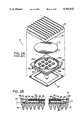
- FIG. 3A is an exploded perspective view of a package of the present invention showing a heatsink on which a plurality of integrated circuit chips are located, an interconnect structure for placing on the heatsink, and a cover having openings for attaching the integrated circuit chips to the interconnect structure.
- FIG. 3B is a cross-sectional view of a portion of an interconnect structure such as shown in FIG. 3A.
- FIG. 3C is a cross-sectional side view of an assembled package such as shown in exploded view in FIG. 3A.
- FIGS. 4A, 4B, and 4C are cross-sectional side views of an interconnect structure and an integrated circuit chip connected by wire bonds, TAB bonds and solder bumps respectively.
- FIGS. 4D and 4E are plan view of typical TAB structures which provide for connection to integrated circuit structures at their centers.
- FIG. 5A is a cut-away side cross-sectional view showing an embodiment of the invention in which the interconnect structure is located on the floor of the package and the integrated circuit chips are located on the ceiling of the package.
- FIG. 5B shows an enlarged view of a structure similar to that of FIG. 5A in which the chip is pressed against the heatsink by an elastomeric disk.
- FIG. 5C shows an enlarged view of a clip used in the structure of FIG. 5A.
- FIG. 6 is a cross-sectional side view of an interconnect structure formed integrally with a plurality of pins extending to the exterior of the package.
- FIG. 7 is a side cross-sectional view of an integrated circuit structure having pins ending flush with the outer surface of the package for solder bump bonding application.
- FIG. 8 is a side cross-sectional view of an embodiment using wire bonds as shown in FIG. 4A and including a resistor and capacitor as shown in FIG. 2B.
- FIGS. 9A through 9C are cross-sectional side views of an interconnect structure and an integrated circuit chip connected by wire bonds, TAB bonds and solder bumps respectively.
- FIGS. 3A-3C illustrate a first embodiment of the present invention.
- heatsink 104 includes means for cooling which in this case is a means for circulating a fluid through pipe 106.
- Attached to the upper surface 104A of heatsink 104 are a plurality, in this case four, of integrated circuit chips 110A, 110B, 110C, and 110D.
- Interconnect structure 114 fits onto heatsink 104 such that apertures 116 surround each of the integrated circuit chips 110A through 110D.
- Various levels of dielectric-encapsulated metallization 202, 210 are seen on the interconnect structure 114 with vias 212 extending to or between those levels.
- interconnect structure 114 When assembled, interconnect structure 114 is separated in space from each of integrated circuit chips 110A through 110D but interconnected electrically through wiring means 118 (see FIG. 3C).
- Integrated circuit chips 110A, 110B, 110C, 110D, (see also FIG. 3A) are bonded in spaced positions, by suitable heat conductive adhesive means 112 (see FIG. 3C) such as silver filled epoxy or solder, to the inwardly-facing surface 104A of heatsink 104.
- suitable heat conductive adhesive means 112 see FIG. 3C
- each chip 110A, 110B, etc. sits in an aperture 116 in interconnect structure 114.
- a frame 124 preferably plastic or ceramic, covers interconnect structure 114 and chips 110A through 110D, forming in combination with heatsink 104 a sealed package which protects the chips and the interconnect structure.
- Frame 124 can be bonded to or mechanically attached to the interconnect structure 114 and has apertures or chip wells 128 which are aligned with interconnect structure apertures 116 and which allow access for wire bonding or repair.
- Rectangular elongated slots 132 are provided near each edge of the frame 124 extending essentially the length of the corresponding edge of underlying interconnect structure 114.
- a depending peripheral rim 126 of frame 124 surrounds the periphery of the interconnect structure 114 when the parts are assembled.
- Chip lids such as 130B of plastic or ceramic are bonded to frame 124 by thermal fusion (plastic-to-plastic), epoxy, or solder (metal plated ceramic lid to metal plated ceramic frame) to cover the chip wells or apertures 128 after wire bonding of the connect pads 120 on each of the chips and connect pads 122 on the interconnect structure.
- Elastomeric conducting strips 134 such as Tecknit Zebra Series 7000/8000 (more clearly shown in FIG. 3A) are positioned in slots 132 and when assembled and compressed on the mother board 102 (FIG. 1) electrically connect contact pads or traces 138 on the mother board to the contact pads 136 on the periphery of the interconnect structure.
- anchoring/alignment pins 300 extend from the frame 124 and upon assembly pass through pin apertures 302 into the heatsink, after which the pins are secured. If the pins are plastic the pins may be secured by melting the protruding end of each pin into a ball 150, which prevents retraction of the pin. Alternatively, if the pin is threaded metal (i.e., a bolt, not shown) a nut may be used to retain the pin. The end result is positive alignment and firm retention of the frame to the heatsink enclosing the interconnect structure and chips.
- Mounting apertures 306 are provided at each corner of the heatsink 104 for mounting bolts 140 (see FIG. 3C). The glass interconnect structure 114 may be mitered at each corner 88 to provide access for the package mounting bolts 140 to the mating holes 306 in the heatsink 104.
- FIG. 3C Shown in FIG. 3C are interchip interconnects 118 and package-to-mother board interconnect assemblies 134.
- the package is shown as mounted on a printed circuit mother board 102.
- the package 100 is constructed by first providing metal heatsink 104, preferably of rectangular or square plan configuration.
- Heatsink 104 in a preferred embodiment is Kovar or molybdenum metal.
- coolant passages 106 can be provided within the heatsink 104 through which a fluid coolant such as water, air or Freon may be circulated for cooling, or the heatsink can be provided with fins for air cooling. Arrows illustrate the inflow and outflow of the coolant along passages 106.
- An optically flat glass or quartz substrate 200 see FIG.
- interconnect structure 114 (made of a low thermal expansion glass so as to thermally match the silicon chips).
- interconnect lines 202, 206, 215 interlaced with electrical insulation material 204, 208 to form multilayer structure 114 including a plurality of interconnect lines, each line extending from a pad 122 (see FIG. 3A perspective view), to which a chip will be connected, to another pad 122, to which a chip will be connected, or to a pad 136, which will be connected to the exterior of the package.
- the layers of interconnect structure 114 are shown in more detail in FIG. 3B, and are discussed below.
- Interconnect structure 114 is preferably epoxy or solder bonded to the heatsink surface 104A with the apertures 116 in interconnect structure 114 peripherally surrounding the chips 110A, 110B, etc.
- the back side 114a of the interconnect structure 114 can be coated with a suitable solderable metal such as nickel.
- Wire bonds 118 see FIG. 3C, also FIG. 4A
- tape automated bonding (TAB) electrical connections 222 are made between chip connect pads 120 on the periphery of chips 110A, 110B, 110C, and 110D to pads 122 on interconnect structure 114 to electrically connect the chips.
- FIG. 4D and 4E show in plan view typical TAB structures to the center of which an integrated circuit chip can be bonded. As shown in FIG. 4D, line end 7 is available for bonding to a corresponding pad in a chip and line end 8 is available for bonding to a pad in the interconnect structure.
- FIG. 4E shows another TAB structure for a chip having fewer bonding pads. After the TAB structure of FIGS. 4D and 4E are bonded to the interconnect structure, the exterior metal comprising portions 9, 10 and 11 of FIG. 4D and portions outside the dotted line 12 of FIG. 4E are removed, thus electrically separating the plurality of leads.
- an insulating frame 124 typically of ceramic or plastic insulating material is mounted over interconnect structure 114 and the chips 110A-110D, and attached to heatsink 104.
- the frame 124 preferably includes apertures 117 having dimensions greater than apertures 116 to provide clearance for, and access to, wire bonds 118.
- Chip lids such as 130B fit into mating recessed areas 128 and close each of the apertures 117, shielding the chips 110A-110D located beneath. Chip lids such as 130B may be pressed, epoxied, thermally fused or soldered in place depending on the material used and the level of chip protection desired.
- Peripheral slots 132 are provided along each peripheral edge of frame 124, and elastomeric connector strips 134 are positioned in the slots to connect contact pads 136 on the glass interconnect structure to contact pads 138 on mother board 102 (see FIG. 3C) when the package 100 is mounted thereon.
- Package 100 is mounted to the mother board 102 by compression screws 140 and nuts 142 extending through mother board 102 and an outer flange portion 144 of heatsink 104.
- Compression-limiting spacers 146 extend between inner surface 102A of mother board 102 and inner surface 104A of the heatsink 104.
- the resultant clamping action mounts package 100 to board 102 and ensures electrical contact between contacts 136 on interconnect structure 114 and contacts 138 on mother board 102 through connection strip 134.
- the resultant structure 100 when mounted, provides a rigid and sealed assembly.
- interconnect structure 114 The high density and short (hence, high speed) interconnects of the present invention are provided by the construction of the interconnect structure 114.
- a preferred form of interconnect structure 114 is seen in FIG. 3B where a typical borosilicate or quartz flat glass plate 200 is provided as a substrate of the interconnect structure.
- the glass plate 200 has a smooth top surface comparable in flatness to a semiconductor wafer, and thus can be processed with equivalent tolerances.
- a first layer 202 of thin film metallization, typically of aluminum and typically 1 micron in thickness, is deposited and delineated using known photolithographic and microetching techniques to form metallization interconnect lines having widths as narrow as 10 microns or less on the top surface of glass plate 200.
- a first dielectric layer 204 preferably of spin-on-glass such as Allied Signal Technologies Accuglass X-11 for planarization, or of silicon dioxide or the like, typically deposited by known chemical vapor deposition techniques, is formed over the first metallization layer 202.
- the dielectric layer 204 can be further planarized, if necessary, by well known mechanical or chemical means, to provide a near-planar top surface, and a second metallization pattern 206 deposited and patterned.
- An additional layer 208 of smoothed dielectric and an additional layer 210 of metallization may be formed thereover resulting in a dense mass of spaced interconnects (traces) and also providing input/output pads for lines to and from the chips.
- vias 212, 214 etc. are etched in the various dielectric layers 204, 208 (respectively) to afford desired connections to and between various levels of metallization in the interconnect structure, as known in the art.
- Thin film resistors such as resistor 250, typically of nichrome, can be integrated into the structure, as well as capacitors such as capacitor 260. Additional layers of metallization and dielectric can be added as desired.
- Multiple interconnect structures 114 can be fabricated using a large master glass plate which is cut apart to form individual interconnect structures. For example, four 10 cm ⁇ 10 cm square interconnect structures can be fabricated on one 20 cm ⁇ 20 cm square glass plate.
- the ability to custom tailor the characteristic impedance of the interconnect structure in accordance with established formulas by any combination of the following: selecting specific thicknesses of the dielectric material(s) 104 and 208, and selecting dielectric material(s) having a differing dielectric constant for use in dielectrics 204 and 208, selecting specific thicknesses of lines 202, 206 and 215 and selecting lateral line-to-line spacing between adjacent lines in a single layer such as 202, 206 or 215. This is true in the case of all the embodiments of this invention.
- FIG. 4A illustrates a schematic partial cross-section of interconnect structure 114 for the first embodiment, in which interconnect structure 114 is mounted on heatsink 104.
- FIG. 4A depicts the attachment of a chip 211 in thermal contact with heatsink 104 for optimum thermal efficiency in cooling of chip 211. Electrical connection of pads 120 of the chip to pads 122 of the interconnect metallization is depicted here and in FIG. 3C using wire bonds 118.
- a chip bonding plate 216 which can be used with all package embodiments described herein to facilitate rework.
- the chip bonding plate 216 is typically of larger dimensions than the chip 211, to facilitate handling, and is of a material, such as molybdenum or Kovar in the case of a silicon chip, that has a close match of thermal expansion coefficient to the chip.
- Chip bonding plate 216 is typically 10 to 15 mils in thickness.
- the attachment of chip 211 to plate 216 is accomplished by using epoxy, gold eutectic bonding, or a high temperature solder 148.
- the chip bonding plate 216 is then attached to the surface 104A of the heat sink 104 in a position which may be surrounded by or adjacent to the interconnect structure 114.
- Attachment of bonded chip bond plate 216 to heatsink 104 is accomplished using a solder 149 having a melting temperature lower than the temperature used for attaching the chip to the plate.
- attachment of TABs 222 (FIG. 4B) to interconnect lines 122 is by thermocompression bonding or by solder 152 having a melting temperature less than the temperature used for attaching chip 211 to plate 216.
- Such attachment is reworkable (i.e.; a defective chip can be removed) by selectively melting the low temperature solder 149 and 152, by localized direction of a heated inert gas such as nitrogen, to remove plate 216 of a defective chip without damaging the interconnect structure or heatsink.
- the location where the defective chip was removed is then cleanable and restorable by removing any residual solder remaining on surface 104A through conventional means, for example a suction device; whereas, if the chip was directly bonded to the heatsink using epoxy without the use of a chip bond plate said epoxy would have a tendency to leave behind difficult-to-remove solids that could greatly hamper rebond.
- the final step in replacement of a defective chip is accomplished by reflow soldering a new chip.
- the chip is attached directly to heatsink 104 using a solder compatible with the chip.
- FIG. 4B follows the same description as FIG. 4A with two exceptions.
- the electrical connection from chip pads 120 to interconnect metallization pads 122 is depicted using TABs 222.
- No chip bonding plate is provided, chip 211 being attached directly to heatsink 104.
- the chip is a type which can tolerate application of solder directly to its back surface (for example a bipolar circuit chip with a silicon substrate which can accept a gold-tin-silicon eutectic solder), the chip 211 may be soldered by solder 151 directly to heatsink 104 and still be removable.
- the chip is attached directly to the interconnect structure with solder bump bonding.
- the embodiment of FIG. 4C shows an interconnect structure having three layers of interconnect metallization 202, 206, and 216 separated by insulation 204 and 218 and selectively connected through vias such as 212 and 214 to form the desired interconnect pattern.
- integrated circuit chip 211 is attached to interconnect structure 114 by means of solder bumps 701 which contact metallization layer 216 in interconnect structure 114.
- the embodiment of FIG. 4C can be used when the chip 211 is a low power device which generates minimum heat and therefore need not be connected to heatsink 104.
- chip 211 When chip 211 will generate high heat the upper surface of chip 211 is thermally connected to a heatsink above chip 211 in a different embodiment.
- the embodiment of FIG. 4C is not preferred when it is desirable to provide for rework to replace chip 211 if defective.
- FIG. 5A depicts an embodiment of the invention in which the integrated circuit chips and the interconnect structure are positioned against opposing surfaces of the interior of the package.
- a multichip package 400 is comprised of a backplate 429 on which is mounted an interconnect structure 426.
- Interconnect structure 426 can be epoxy or solder bond mounted to a backing plate 429 for the purpose of structural strength and protection of the interconnect structure 426.
- the backside 426A of interconnect structure 426 can be coated with a suitable solderable metal such as nickel.
- Interconnect structure 426 and backplate 429 are aligned and retained within the mating pocket of frame 434.
- Frame 434 is of such thickness that when the package is mounted on a printed circuit mother board 404 using screws 431 and nuts 432, proper compression of elastomeric connector 430 is achieved between clips (or flex circuit) 428 and contact pads 433 on printed circuit mother board 404.
- the package also comprises a heatsink 406, typically molybdenum, which may have coolant inlet and outlet flow connections (not shown), or fins 412 for air cooling.
- Backing plate 429 is made of an insulating material such as ceramic or plastic which is rigid enough to support interconnect structure 426 during manufacturing.
- Chip electrical contact pads 420 are connected by tape automated bonding (TAB) film 422 to pads 424 on interconnect structure 426.
- TAB tape automated bonding
- Chips 418A, 418B to which chip bond plates 416A, 416B have been applied are attached to TAB films 422.
- heatsink 104 is brought into contact with chip bond plates 416A, 416B upon which chips 418A, 418B are bonded.
- the chip bond plates 416A, 416B are typically made of molybdenum for thermal matching to the silicon chip and are attached to chips 418A, 418B by epoxy or solder.
- the plates are maintained in intimate thermal contact to heatsink 406 by thermal grease 417 and/or can be clamped to heatsink 408 using miniature clamps 418 which pass through heatsink 406 and are retained by nuts 419.
- clamps are optional, as thermal grease alone achieves good thermal contact.
- chip bond plates 416A and 416B may be omitted and the chip attached directly by thermal grease.
- a resilient, electrically non-conducting elastomeric disk 440 of the approximate size of chip 418b can be placed between chip 418b and interconnect structure 426 such that when heatsink 406 is mounted, elastomeric disk 440 is compressed slightly and thereby transfers pressure to the chip/heatsink interface to achieve good thermal contact.
- TAB 422 can be readily formed in such a way as to allow such displacement of chip 418B as required during the compression process.
- heat generated by the chips 418A, 418B, when operating, is dissipated by heatsink 406 to the coolant or the ambient atmosphere.
- Electrical connections are made from contact pads 435 on the top periphery of the interconnect structure 426 to pads 436 on the bottom of backing plate 429 by spring clips 428.
- a wrap-around flexible circuit such as Bradyflex Flexible Circuitry, which comprises parallel copper leads on a Kapton base are bonded between pads 435 and 436.
- Electrical connection from package 400 to mother board 404 is accomplished through connector 430 (which may be silicon rubber with vertical conductive fibers or a frame including multiple vertically extending pressure contacts) is compressed between clips 428 and mating pads 433 on mother board 404.
- Elastomeric connector 430 is properly positioned and retained by frame 434 which can be molded plastic.
- heatsink 406 also serves as a lid for all the chips 418A, 418B etc. in package 400 and frame 434 serves as the containment structure.
- Frame 434 aligns the contact pads 435 with mating pads 433 by providing surfaces 434A and 434B in its interior corners to provide support and mating containment to the composite of interconnect structure 426 and backing plate 429.
- Inner wall 434C provides containment for the spring clips or the wrap-around flexible circuit, which are bonded to interconnect structure 426 and backing plate 429 typically on each of four sides.
- Flange 406A of heatsink 406 rests on surface 434D of frame 434 and is secured to surface 434D when the package 400 is mounted to printed circuit mother board 404.
- the resultant structure 400 when mounted is rigidly secured and sealed.
- a variation to this embodiment is achieved when the spring clips 428 shown in FIG. 5A are replaced with another common form of these clips which have a "tail" 428A (see FIG. 5C) for direct insertion into through-holes in a printed circuit board.
- Such version would eliminate the elastomeric connector 430 used for surface mount applications.
- FIG. 6 A further embodiment of the invention is partially shown in FIG. 6 wherein laser or otherwise drilled holes are provided in insulating plate 500 (preferably glass or ceramic) with terminal pins 502A, 502B, 502C sealed therein.
- An array of pins represented by pins 502A, 502B, 502C protrude from the lower side 500A of plate 500 for socketing or solder attachment to a printed circuit mother board (not shown) and are flush with the upper side 500B of plate 500.
- Dielectric 504 and metallization 506 are built up on the front side 500B with appropriately etched and metallized vias 508A, 508B, 508C leading to the terminal pins.
- Additional dielectric layer 510 is deposited over metallization layer 506 and etched to form vias such as 514, 516.
- a second metallization layer 512 is then formed over dielectric layer 510.
- Front side electrical interconnection layer 512 equivalent to metal layer 122 of FIG. 4A, is provided for connection to contact pads on the chips (not shown in FIG. 6) by wire bonds or TAB bonds.
- the pins 552A, 552B, 552C can be terminated flush with the bottom 500A of plate 500, to provide an array of flat contacts for solder-bump bonding (surface mount) to a printed circuit mother board.
- a unitary structure comprising metal plate 628 and interconnect structure 629 constructed thereon, which replaces separately manufactured heatsink 104 and interconnect structure 114 of FIG. 1.
- Metal plate 628 not only provides highly efficient, direct, opposite-side heat removal for the chips mounted on plate 628, but serves as a base upon which interconnect structure 629 is constructed.
- Kovar, or other metal such as molybdenum having good thermal conductivity and a good coefficient of thermal expansion match with silicon and silicon dioxide, can be used as the metal of plate 628.
- Onto a preferably planar metal upper surface of substrate 628 is first deposited a layer 601 of silicon nitride or silicon dioxide, 2 to 20 microns thick.
- layer 601 can be spin-on-glass.
- the dielectric layers can be any combination of dielectric materials.
- Layer 601 serves as a base layer for the electrical interconnect just as glass interconnect structure 114 does in the other embodiments.
- the surface of layer 601 can be polished, if necessary, by chemical or mechanical means.
- Multilayer interconnect metallization is then built thereon by semiconductor processing techniques as described previously.
- the embodiment of FIG. 8 shows five insulating layers 601, 603, 605, 607 and 609 separating four conductive metallization layers 602, 604, 606, and 608.
- Layer 608a adjacent layer 608 comprises nichrome or polycrystalline silicon and is used for resistors such as resistor 608a-l.
- Insulating layer 607 comprises a composite of silicon oxide and silicon nitride, and is patterned such that only a thin layer of silicon nitride is present between metallization layers 606 and 608 at extensive region 607c, thereby forming a capacitor.
- the interconnect structure of the present invention differs from an integrated circuit chip in that it does not include active devices.
- the interconnect structures can be made in wafer form with several interconnect structures in an array on the same wafer. The wafer can be cut into individual units by laser or saw after processing. Means of interconnect to a printed circuit mother board and containment and sealing are as described for the other embodiments.
- FIGS. 9A-9C illustrate alternative schematic partial cross-sections of FIG. 8.
- the structures of FIGS. 9A-9C are the same as those of FIGS. 4A-4C except that the interconnect structure 629 is formed on base 628 rather than being attached after manufacture. Therefore, FIGS. 9A-9C are not described in detail.
- the interconnect structure in addition to silicon dioxide, silicon nitride, or sputtered quartz, spin-on-glass or polyimide may also be employed as the dielectric, while the metallization may be copper, gold, or aluminum.
Abstract
Description
Claims (51)
Priority Applications (1)
| Application Number | Priority Date | Filing Date | Title |
|---|---|---|---|
| US07/804,614 US5182632A (en) | 1989-11-22 | 1991-12-02 | High density multichip package with interconnect structure and heatsink |
Applications Claiming Priority (2)
| Application Number | Priority Date | Filing Date | Title |
|---|---|---|---|
| US44054589A | 1989-11-22 | 1989-11-22 | |
| US07/804,614 US5182632A (en) | 1989-11-22 | 1991-12-02 | High density multichip package with interconnect structure and heatsink |
Related Parent Applications (1)
| Application Number | Title | Priority Date | Filing Date |
|---|---|---|---|
| US44054589A Continuation | 1989-11-22 | 1989-11-22 |
Publications (1)
| Publication Number | Publication Date |
|---|---|
| US5182632A true US5182632A (en) | 1993-01-26 |
Family
ID=27032450
Family Applications (1)
| Application Number | Title | Priority Date | Filing Date |
|---|---|---|---|
| US07/804,614 Expired - Fee Related US5182632A (en) | 1989-11-22 | 1991-12-02 | High density multichip package with interconnect structure and heatsink |
Country Status (1)
| Country | Link |
|---|---|
| US (1) | US5182632A (en) |
Cited By (85)
| Publication number | Priority date | Publication date | Assignee | Title |
|---|---|---|---|---|
| US5295082A (en) * | 1989-02-22 | 1994-03-15 | The Boeing Company | Efficient method for multichip module interconnect |
| US5468992A (en) * | 1991-02-28 | 1995-11-21 | Hitachi, Ltd. | Electronic circuit package including plural bare chips mounted on a single wiring substrate |
| US5475263A (en) * | 1994-02-14 | 1995-12-12 | Delco Electronics Corp. | Thick film hybrid multilayer circuit |
| US5477082A (en) * | 1994-01-11 | 1995-12-19 | Exponential Technology, Inc. | Bi-planar multi-chip module |
| US5546297A (en) * | 1993-08-31 | 1996-08-13 | Advanced Micro Devices, Inc. | Apparatus for modifying an electrical signal |
| US5548481A (en) * | 1993-04-05 | 1996-08-20 | Ford Motor Company | Electronic module containing an internally ribbed, integral heat sink and bonded, flexible printed wiring board with two-sided component population |
| US5557503A (en) * | 1995-05-12 | 1996-09-17 | International Business Machines Corporation | Circuit card having a large module strain relief and heat sink support |
| US5561328A (en) * | 1991-06-24 | 1996-10-01 | Digital Equipment Corporation | Photo-definable template for semiconductor chip alignment |
| US5615087A (en) * | 1994-08-18 | 1997-03-25 | Allen-Bradley Company, Inc. | Insulated surface mount circuit board construction |
| DE19645971A1 (en) * | 1995-12-08 | 1997-06-12 | Hewlett Packard Co | Housing system, for field effect transistors |
| EP0807369A1 (en) * | 1995-01-23 | 1997-11-19 | Irvine Sensors Corporation | Stackable modules and multimodular assemblies |
| US5710071A (en) * | 1995-12-04 | 1998-01-20 | Motorola, Inc. | Process for underfilling a flip-chip semiconductor device |
| US5766975A (en) * | 1995-01-09 | 1998-06-16 | Integrated Device Technology, Inc. | Packaged integrated circuit having thermal enhancement and reduced footprint size |
| US5793150A (en) * | 1994-07-07 | 1998-08-11 | Firma Carl Freudenberg | Flat seal |
| US5801452A (en) * | 1996-10-25 | 1998-09-01 | Micron Technology, Inc. | Multi chip module including semiconductor wafer or dice, interconnect substrate, and alignment member |
| US5811879A (en) * | 1996-06-26 | 1998-09-22 | Micron Technology, Inc. | Stacked leads-over-chip multi-chip module |
| US5898571A (en) * | 1997-04-28 | 1999-04-27 | Lsi Logic Corporation | Apparatus and method for clip-on attachment of heat sinks to encapsulated semiconductor packages |
| US5899705A (en) * | 1997-11-20 | 1999-05-04 | Akram; Salman | Stacked leads-over chip multi-chip module |
| US5905305A (en) * | 1996-01-24 | 1999-05-18 | Micron Technology, Inc. | Condensed memory matrix |
| US5915754A (en) * | 1995-06-27 | 1999-06-29 | Braun Aktiengesellschaft | Method of mounting an electronic power component |
| US5963429A (en) * | 1997-08-20 | 1999-10-05 | Sulzer Intermedics Inc. | Printed circuit substrate with cavities for encapsulating integrated circuits |
| US5977622A (en) * | 1997-04-25 | 1999-11-02 | Lsi Logic Corporation | Stiffener with slots for clip-on heat sink attachment |
| US6008538A (en) * | 1996-10-08 | 1999-12-28 | Micron Technology, Inc. | Method and apparatus providing redundancy for fabricating highly reliable memory modules |
| US6011304A (en) * | 1997-05-05 | 2000-01-04 | Lsi Logic Corporation | Stiffener ring attachment with holes and removable snap-in heat sink or heat spreader/lid |
| US6016005A (en) * | 1998-02-09 | 2000-01-18 | Cellarosi; Mario J. | Multilayer, high density micro circuit module and method of manufacturing same |
| US6043560A (en) * | 1997-12-03 | 2000-03-28 | Intel Corporation | Thermal interface thickness control for a microprocessor |
| US6046503A (en) * | 1997-09-26 | 2000-04-04 | Siemens Aktiengesellschaft | Metalization system having an enhanced thermal conductivity |
| US6119675A (en) * | 1996-11-12 | 2000-09-19 | Micron Technology, Inc. | Method for sawing wafers employing multiple indexing techniques for multiple die dimensions |
| US6166554A (en) * | 1996-03-27 | 2000-12-26 | Electronics Products Company | Flexible electrical test fixture for integrated circuits on prototype and production printed circuit boards |
| EP1071131A1 (en) * | 1997-08-22 | 2001-01-24 | Raytheon Company | Large non-hermetic multichip module package |
| US6208526B1 (en) * | 1999-07-23 | 2001-03-27 | Motorola, Inc. | Mounting multiple substrate frame and leadless surface mountable assembly using same |
| US6215175B1 (en) | 1998-07-06 | 2001-04-10 | Micron Technology, Inc. | Semiconductor package having metal foil die mounting plate |
| EP1093004A2 (en) * | 1999-10-01 | 2001-04-18 | Lucent Technologies Inc. | Hybrid electro-optic device with combined mirror arrays |
| US6303981B1 (en) | 1999-09-01 | 2001-10-16 | Micron Technology, Inc. | Semiconductor package having stacked dice and leadframes and method of fabrication |
| US6349465B1 (en) * | 1996-03-28 | 2002-02-26 | Intel Corporation | Controlled bondline thickness attachment mechanism |
| US6377464B1 (en) * | 1999-01-29 | 2002-04-23 | Conexant Systems, Inc. | Multiple chip module with integrated RF capabilities |
| US6414391B1 (en) | 1998-06-30 | 2002-07-02 | Micron Technology, Inc. | Module assembly for stacked BGA packages with a common bus bar in the assembly |
| US6421251B1 (en) * | 1997-05-02 | 2002-07-16 | Axis Systems Inc | Array board interconnect system and method |
| US20030025196A1 (en) * | 2001-08-01 | 2003-02-06 | Hitachi, Ltd. | Heat transfer structure and a semi-conductor device |
| US6601753B2 (en) * | 2001-05-17 | 2003-08-05 | Visteon Global Technologies, Inc. | Void-free die attachment method with low melting metal |
| US20030173674A1 (en) * | 2002-03-12 | 2003-09-18 | Fujitsu Limited | Semiconductor device and method for fabricating the same |
| US6627991B1 (en) * | 1998-08-05 | 2003-09-30 | Fairchild Semiconductor Corporation | High performance multi-chip flip package |
| US20030194483A1 (en) * | 2002-04-12 | 2003-10-16 | International Business Machines Corporation | Grease rework applicator |
| US20030214234A1 (en) * | 2002-05-20 | 2003-11-20 | Ushiodenki Kabushiki Kaisha | Discharge lamp |
| US6680853B1 (en) * | 2003-01-27 | 2004-01-20 | Hewlett-Packard Development Company, L.P. | Systems and methods for mounting components to circuit assemblies |
| US6713854B1 (en) * | 2000-10-16 | 2004-03-30 | Legacy Electronics, Inc | Electronic circuit module with a carrier having a mounting pad array |
| US20040092179A1 (en) * | 2002-11-12 | 2004-05-13 | O'rourke Maurice C. | Reset speed control for watercraft |
| US6815251B1 (en) | 1999-02-01 | 2004-11-09 | Micron Technology, Inc. | High density modularity for IC's |
| US20050040510A1 (en) * | 1999-10-01 | 2005-02-24 | Seiko Epson Corporation | Interconnect substrate, semiconductor device, methods of fabricating, inspecting, and mounting the semiconductor device, circuit board, and electronic instrument |
| US6868217B1 (en) * | 2000-07-31 | 2005-03-15 | Cisco Technology, Inc. | Long reach unamplified optical SONET/SDH card |
| US20050156281A1 (en) * | 2004-01-19 | 2005-07-21 | International Business Machines Corporation | HIGH TOLERANCE TCR BALANCED HIGH CURRENT RESISTOR FOR RF CMOS AND RF SiGe BiCMOS APPLICATIONS AND CADENCED BASED HIERARCHICAL PARAMETERIZED CELL DESIGN KIT WITH TUNABLE TCR AND ESD RESISTOR BALLASTING FEATURE |
| US20050180117A1 (en) * | 2004-02-18 | 2005-08-18 | Nec Electronics Corporation | Semiconductor device and method of manufacturing the same |
| US20050269677A1 (en) * | 2004-05-28 | 2005-12-08 | Martin Standing | Preparation of front contact for surface mounting |
| US20060118447A1 (en) * | 2004-12-02 | 2006-06-08 | Pei Chen | Direct cooling pallet assembly for temperature stability for deep ion mill etch process |
| US20060214284A1 (en) * | 2005-03-24 | 2006-09-28 | Stuart Haden | Apparatus and method for data capture |
| US20060220123A1 (en) * | 2000-04-04 | 2006-10-05 | International Rectifier Corporation | Chip scale surface mounted device and process of manufacture |
| US20060240598A1 (en) * | 2005-04-20 | 2006-10-26 | International Rectifier Corporation | Chip scale package |
| US20060237840A1 (en) * | 2005-04-21 | 2006-10-26 | International Rectifier Corporation | Semiconductor package |
| US20070012947A1 (en) * | 2002-07-15 | 2007-01-18 | International Rectifier Corporation | Direct FET device for high frequency application |
| US20070080458A1 (en) * | 2005-10-11 | 2007-04-12 | Tsuyoshi Ogawa | Hybrid module and method of manufacturing the same |
| US20070111562A1 (en) * | 2001-08-03 | 2007-05-17 | Wallace Robert F | Circuit Board Manufacturing Technique and Resulting Circuit Board |
| US20070284720A1 (en) * | 2006-05-10 | 2007-12-13 | Infineon Technologies Ag | Power semiconductor device and method for its production |
| US20080017797A1 (en) * | 2006-07-21 | 2008-01-24 | Zhaohui Cheng | Pattern inspection and measurement apparatus |
| US20080054429A1 (en) * | 2006-08-25 | 2008-03-06 | Bolken Todd O | Spacers for separating components of semiconductor device assemblies, semiconductor device assemblies and systems including spacers and methods of making spacers |
| US7442582B2 (en) | 1997-07-14 | 2008-10-28 | Infineon Technologies Ag | Method for producing a chip-substrate connection |
| US20090056997A1 (en) * | 2007-08-28 | 2009-03-05 | Occam Portfolio Llc | Electronic Assemblies Without Solder and Methods for their Manufacture |
| US7579697B2 (en) | 2002-07-15 | 2009-08-25 | International Rectifier Corporation | Arrangement for high frequency application |
| US20100038781A1 (en) * | 2008-08-14 | 2010-02-18 | Dongsam Park | Integrated circuit packaging system having a cavity |
| USRE41559E1 (en) | 2001-10-10 | 2010-08-24 | International Rectifier Corporation | Semiconductor device package with improved cooling |
| USRE43404E1 (en) | 1996-03-07 | 2012-05-22 | Tessera, Inc. | Methods for providing void-free layer for semiconductor assemblies |
| US8466546B2 (en) | 2005-04-22 | 2013-06-18 | International Rectifier Corporation | Chip-scale package |
| US20140015387A1 (en) * | 2012-07-13 | 2014-01-16 | International Business Machines Corporation | Non-hermetic sealed multi-chip module package |
| US8689159B1 (en) * | 2012-09-12 | 2014-04-01 | Nvidia Corporation | Redundancy for on-chip interconnect |
| US8941430B2 (en) * | 2012-09-12 | 2015-01-27 | Nvidia Corporation | Timing calibration for on-chip interconnect |
| US9089051B2 (en) | 2013-06-27 | 2015-07-21 | International Business Machines Corporation | Multichip module with stiffening frame and associated covers |
| US20150235930A1 (en) * | 2014-02-17 | 2015-08-20 | Mitsubishi Electric Corporation | Package of power dies and three-phase power converter |
| US20150305191A1 (en) * | 2014-04-18 | 2015-10-22 | Raytheon Company | Method to align surface mount packages for thermal enhancement |
| US20180070447A1 (en) * | 2013-07-09 | 2018-03-08 | Oleson Convergent Solutions Llc | Packaging for high power integrated circuits and infrared emitter arrays |
| US9997476B2 (en) | 2015-10-30 | 2018-06-12 | Infineon Technologies Ag | Multi-die package having different types of semiconductor dies attached to the same thermally conductive flange |
| CN109616451A (en) * | 2015-03-31 | 2019-04-12 | 克里公司 | Multi-cavity packaging part with single metal flange |
| US10455685B1 (en) * | 2018-10-15 | 2019-10-22 | Intel Corporation | Electronic device, socket, and spacer to alter socket profile |
| US20200294924A1 (en) * | 2012-12-20 | 2020-09-17 | Intel Corporation | High density organic bridge device and method |
| US10833051B2 (en) | 2019-01-24 | 2020-11-10 | International Business Machines Corporation | Precision alignment of multi-chip high density interconnects |
| US11031373B2 (en) | 2019-03-29 | 2021-06-08 | International Business Machines Corporation | Spacer for die-to-die communication in an integrated circuit |
| WO2021167596A1 (en) * | 2020-02-19 | 2021-08-26 | Pierburg Gmbh | Electric power module |
Citations (11)
| Publication number | Priority date | Publication date | Assignee | Title |
|---|---|---|---|---|
| US4544989A (en) * | 1980-06-30 | 1985-10-01 | Sharp Kabushiki Kaisha | Thin assembly for wiring substrate |
| US4677526A (en) * | 1984-03-01 | 1987-06-30 | Augat Inc. | Plastic pin grid array chip carrier |
| US4731699A (en) * | 1985-10-08 | 1988-03-15 | Nec Corporation | Mounting structure for a chip |
| US4742024A (en) * | 1986-09-17 | 1988-05-03 | Fujitsu Limited | Semiconductor device and method of producing semiconductor device |
| US4744007A (en) * | 1983-03-29 | 1988-05-10 | Nec Corporation | High density LSI package for logic circuits |
| US4751482A (en) * | 1983-12-23 | 1988-06-14 | Fujitsu Limited | Semiconductor integrated circuit device having a multi-layered wiring board for ultra high speed connection |
| US4823234A (en) * | 1985-08-16 | 1989-04-18 | Dai-Ichi Seiko Co., Ltd. | Semiconductor device and its manufacture |
| US4835598A (en) * | 1985-06-13 | 1989-05-30 | Matsushita Electric Works, Ltd. | Wiring board |
| US4860165A (en) * | 1988-04-27 | 1989-08-22 | Prime Computer, Inc. | Semiconductor chip carrier package |
| US4873615A (en) * | 1986-10-09 | 1989-10-10 | Amp Incorporated | Semiconductor chip carrier system |
| US4939570A (en) * | 1988-07-25 | 1990-07-03 | International Business Machines, Corp. | High power, pluggable tape automated bonding package |
-
1991
- 1991-12-02 US US07/804,614 patent/US5182632A/en not_active Expired - Fee Related
Patent Citations (11)
| Publication number | Priority date | Publication date | Assignee | Title |
|---|---|---|---|---|
| US4544989A (en) * | 1980-06-30 | 1985-10-01 | Sharp Kabushiki Kaisha | Thin assembly for wiring substrate |
| US4744007A (en) * | 1983-03-29 | 1988-05-10 | Nec Corporation | High density LSI package for logic circuits |
| US4751482A (en) * | 1983-12-23 | 1988-06-14 | Fujitsu Limited | Semiconductor integrated circuit device having a multi-layered wiring board for ultra high speed connection |
| US4677526A (en) * | 1984-03-01 | 1987-06-30 | Augat Inc. | Plastic pin grid array chip carrier |
| US4835598A (en) * | 1985-06-13 | 1989-05-30 | Matsushita Electric Works, Ltd. | Wiring board |
| US4823234A (en) * | 1985-08-16 | 1989-04-18 | Dai-Ichi Seiko Co., Ltd. | Semiconductor device and its manufacture |
| US4731699A (en) * | 1985-10-08 | 1988-03-15 | Nec Corporation | Mounting structure for a chip |
| US4742024A (en) * | 1986-09-17 | 1988-05-03 | Fujitsu Limited | Semiconductor device and method of producing semiconductor device |
| US4873615A (en) * | 1986-10-09 | 1989-10-10 | Amp Incorporated | Semiconductor chip carrier system |
| US4860165A (en) * | 1988-04-27 | 1989-08-22 | Prime Computer, Inc. | Semiconductor chip carrier package |
| US4939570A (en) * | 1988-07-25 | 1990-07-03 | International Business Machines, Corp. | High power, pluggable tape automated bonding package |
Non-Patent Citations (6)
| Title |
|---|
| A. C. Adams et al., "Advanced Packaging for VLSI-Based Systems", Suss Report, Nov. 1987, pp. 2-3. |
| A. C. Adams et al., Advanced Packaging for VLSI Based Systems , Suss Report, Nov. 1987, pp. 2 3. * |
| Bill Blood and Allison Casey, "Evaluating MCM Packaging Technology", ASIC Technology and News, Aug. 1991, vol. 3, No. 4, p. 22. |
| Bill Blood and Allison Casey, Evaluating MCM Packaging Technology , ASIC Technology and News, Aug. 1991, vol. 3, No. 4, p. 22. * |
| R. E. Thun et al., "Section B-17: Printed and Molded Circuits; Integrated Microcircuits", Insulation/Circuits--Directory/Encyclopedia Issue, Jun./Jul. 1971, pp. 217-231. |
| R. E. Thun et al., Section B 17: Printed and Molded Circuits; Integrated Microcircuits , Insulation/Circuits Directory/Encyclopedia Issue, Jun./Jul. 1971, pp. 217 231. * |
Cited By (177)
| Publication number | Priority date | Publication date | Assignee | Title |
|---|---|---|---|---|
| US5295082A (en) * | 1989-02-22 | 1994-03-15 | The Boeing Company | Efficient method for multichip module interconnect |
| US20070158814A1 (en) * | 1991-02-28 | 2007-07-12 | Nobuyasu Kanekawa | Electronic circuit package |
| US7120069B2 (en) | 1991-02-28 | 2006-10-10 | Hitachi, Ltd. | Electronic circuit package |
| US7233534B2 (en) | 1991-02-28 | 2007-06-19 | Hitachi, Ltd. | Electronic circuit package |
| US20080303175A1 (en) * | 1991-02-28 | 2008-12-11 | Nobuyasu Kanekawa | Electronic circuit package |
| US6728904B2 (en) | 1991-02-28 | 2004-04-27 | Hitachi, Ltd. | Electronic circuit package |
| US7425763B2 (en) | 1991-02-28 | 2008-09-16 | Hitachi, Ltd. | Electronic circuit package |
| US6584004B2 (en) | 1991-02-28 | 2003-06-24 | Hitachi, Ltd. | Electronic circuit package |
| US5468992A (en) * | 1991-02-28 | 1995-11-21 | Hitachi, Ltd. | Electronic circuit package including plural bare chips mounted on a single wiring substrate |
| US20040164324A1 (en) * | 1991-02-28 | 2004-08-26 | Nobuyasu Kanekawa | Electronic circuit package |
| US7701743B2 (en) | 1991-02-28 | 2010-04-20 | Rising Silicon, Inc. | Electronic circuit package |
| US6223273B1 (en) | 1991-02-28 | 2001-04-24 | Hitachi, Ltd. | Electronic circuit package |
| US5561328A (en) * | 1991-06-24 | 1996-10-01 | Digital Equipment Corporation | Photo-definable template for semiconductor chip alignment |
| US5548481A (en) * | 1993-04-05 | 1996-08-20 | Ford Motor Company | Electronic module containing an internally ribbed, integral heat sink and bonded, flexible printed wiring board with two-sided component population |
| US5546297A (en) * | 1993-08-31 | 1996-08-13 | Advanced Micro Devices, Inc. | Apparatus for modifying an electrical signal |
| US5477082A (en) * | 1994-01-11 | 1995-12-19 | Exponential Technology, Inc. | Bi-planar multi-chip module |
| US5475263A (en) * | 1994-02-14 | 1995-12-12 | Delco Electronics Corp. | Thick film hybrid multilayer circuit |
| US5793150A (en) * | 1994-07-07 | 1998-08-11 | Firma Carl Freudenberg | Flat seal |
| US6031723A (en) * | 1994-08-18 | 2000-02-29 | Allen-Bradley Company, Llc | Insulated surface mount circuit board construction |
| US5615087A (en) * | 1994-08-18 | 1997-03-25 | Allen-Bradley Company, Inc. | Insulated surface mount circuit board construction |
| US5766975A (en) * | 1995-01-09 | 1998-06-16 | Integrated Device Technology, Inc. | Packaged integrated circuit having thermal enhancement and reduced footprint size |
| US5874321A (en) * | 1995-01-09 | 1999-02-23 | Integrated Device Technology, Inc. | Package integrated circuit having thermal enhancement and reduced footprint size |
| EP0807369A1 (en) * | 1995-01-23 | 1997-11-19 | Irvine Sensors Corporation | Stackable modules and multimodular assemblies |
| EP0807369A4 (en) * | 1995-01-23 | 1999-11-17 | Irvine Sensors Corp | Stackable modules and multimodular assemblies |
| US5557503A (en) * | 1995-05-12 | 1996-09-17 | International Business Machines Corporation | Circuit card having a large module strain relief and heat sink support |
| US5915754A (en) * | 1995-06-27 | 1999-06-29 | Braun Aktiengesellschaft | Method of mounting an electronic power component |
| US5710071A (en) * | 1995-12-04 | 1998-01-20 | Motorola, Inc. | Process for underfilling a flip-chip semiconductor device |
| DE19645971A1 (en) * | 1995-12-08 | 1997-06-12 | Hewlett Packard Co | Housing system, for field effect transistors |
| DE19645971C2 (en) * | 1995-12-08 | 2002-02-28 | Agilent Technologies Inc | Housing system with field effect transistors and method for housing field effect transistors |
| US6307262B1 (en) | 1996-01-24 | 2001-10-23 | Micron Technology, Inc. | Condensed memory matrix |
| US5977629A (en) * | 1996-01-24 | 1999-11-02 | Micron Technology, Inc. | Condensed memory matrix |
| US5905305A (en) * | 1996-01-24 | 1999-05-18 | Micron Technology, Inc. | Condensed memory matrix |
| US6071757A (en) * | 1996-01-24 | 2000-06-06 | Micron Technology, Inc. | Condensed memory matrix |
| US6620706B2 (en) | 1996-01-24 | 2003-09-16 | Micron Technology, Inc. | Condensed memory matrix |
| US6133630A (en) * | 1996-01-24 | 2000-10-17 | Micron Technology, Inc. | Condensed memory matrix |
| USRE43404E1 (en) | 1996-03-07 | 2012-05-22 | Tessera, Inc. | Methods for providing void-free layer for semiconductor assemblies |
| US6166554A (en) * | 1996-03-27 | 2000-12-26 | Electronics Products Company | Flexible electrical test fixture for integrated circuits on prototype and production printed circuit boards |
| US6349465B1 (en) * | 1996-03-28 | 2002-02-26 | Intel Corporation | Controlled bondline thickness attachment mechanism |
| US6091143A (en) * | 1996-06-26 | 2000-07-18 | Micron Technology, Inc. | Stacked leads-over chip multi-chip module |
| US6300163B1 (en) | 1996-06-26 | 2001-10-09 | Micron Technology, Inc. | Stacked leads-over-chip multi-chip module |
| US6707141B2 (en) | 1996-06-26 | 2004-03-16 | Micron Technology, Inc. | Multi-chip module substrate for use with leads-over chip type semiconductor devices |
| US6104089A (en) * | 1996-06-26 | 2000-08-15 | Micron Technology, Inc. | Stacked leads-over chip multi-chip module |
| US5811879A (en) * | 1996-06-26 | 1998-09-22 | Micron Technology, Inc. | Stacked leads-over-chip multi-chip module |
| US6841868B2 (en) | 1996-10-08 | 2005-01-11 | Micron Technology, Inc. | Memory modules including capacity for additional memory |
| US6720652B2 (en) | 1996-10-08 | 2004-04-13 | Micron Technology, Inc. | Apparatus providing redundancy for fabricating highly reliable memory modules |
| US6060339A (en) * | 1996-10-08 | 2000-05-09 | Micron Technology, Inc. | Method and apparatus providing redundancy for fabricating highly reliable memory modules |
| US6008538A (en) * | 1996-10-08 | 1999-12-28 | Micron Technology, Inc. | Method and apparatus providing redundancy for fabricating highly reliable memory modules |
| US6274390B1 (en) | 1996-10-08 | 2001-08-14 | Micron Technology, Inc. | Method and apparatus providing redundancy for fabricating highly reliable memory modules |
| US6215181B1 (en) | 1996-10-08 | 2001-04-10 | Micron Technology, Inc. | Method and apparatus providing redundancy for fabricating highly reliable memory modules |
| US6531772B2 (en) | 1996-10-08 | 2003-03-11 | Micron Technology, Inc. | Electronic system including memory module with redundant memory capability |
| US6077723A (en) * | 1996-10-25 | 2000-06-20 | Micron Technology, Inc. | Method for fabricating a multi chip module with alignment member |
| US5801452A (en) * | 1996-10-25 | 1998-09-01 | Micron Technology, Inc. | Multi chip module including semiconductor wafer or dice, interconnect substrate, and alignment member |
| US7387119B2 (en) | 1996-11-12 | 2008-06-17 | Micron Technology, Inc. | Dicing saw with variable indexing capability |
| US20050211236A1 (en) * | 1996-11-12 | 2005-09-29 | Salman Akram | Dicing saw with variable indexing capability |
| US6119675A (en) * | 1996-11-12 | 2000-09-19 | Micron Technology, Inc. | Method for sawing wafers employing multiple indexing techniques for multiple die dimensions |
| US5977622A (en) * | 1997-04-25 | 1999-11-02 | Lsi Logic Corporation | Stiffener with slots for clip-on heat sink attachment |
| US5898571A (en) * | 1997-04-28 | 1999-04-27 | Lsi Logic Corporation | Apparatus and method for clip-on attachment of heat sinks to encapsulated semiconductor packages |
| US6421251B1 (en) * | 1997-05-02 | 2002-07-16 | Axis Systems Inc | Array board interconnect system and method |
| US6011304A (en) * | 1997-05-05 | 2000-01-04 | Lsi Logic Corporation | Stiffener ring attachment with holes and removable snap-in heat sink or heat spreader/lid |
| US7442582B2 (en) | 1997-07-14 | 2008-10-28 | Infineon Technologies Ag | Method for producing a chip-substrate connection |
| US5963429A (en) * | 1997-08-20 | 1999-10-05 | Sulzer Intermedics Inc. | Printed circuit substrate with cavities for encapsulating integrated circuits |
| EP1071131A1 (en) * | 1997-08-22 | 2001-01-24 | Raytheon Company | Large non-hermetic multichip module package |
| US6046503A (en) * | 1997-09-26 | 2000-04-04 | Siemens Aktiengesellschaft | Metalization system having an enhanced thermal conductivity |
| US5899705A (en) * | 1997-11-20 | 1999-05-04 | Akram; Salman | Stacked leads-over chip multi-chip module |
| US5936305A (en) * | 1997-11-20 | 1999-08-10 | Micron Technology, Inc. | Stacked leads-over chip multi-chip module |
| US6043560A (en) * | 1997-12-03 | 2000-03-28 | Intel Corporation | Thermal interface thickness control for a microprocessor |
| US6016005A (en) * | 1998-02-09 | 2000-01-18 | Cellarosi; Mario J. | Multilayer, high density micro circuit module and method of manufacturing same |
| US6242286B1 (en) | 1998-02-09 | 2001-06-05 | Mario J. Cellarosi | Multilayer high density micro circuit module and method of manufacturing same |
| US6414391B1 (en) | 1998-06-30 | 2002-07-02 | Micron Technology, Inc. | Module assembly for stacked BGA packages with a common bus bar in the assembly |
| US20060051953A1 (en) * | 1998-06-30 | 2006-03-09 | Corisis David J | Module assembly and method for stacked BGA packages |
| US7408255B2 (en) | 1998-06-30 | 2008-08-05 | Micron Technology, Inc. | Assembly for stacked BGA packages |
| US7400032B2 (en) | 1998-06-30 | 2008-07-15 | Micron Technology, Inc. | Module assembly for stacked BGA packages |
| US6838768B2 (en) | 1998-06-30 | 2005-01-04 | Micron Technology Inc | Module assembly for stacked BGA packages |
| US7279797B2 (en) | 1998-06-30 | 2007-10-09 | Micron Technology, Inc. | Module assembly and method for stacked BGA packages |
| US20060049504A1 (en) * | 1998-06-30 | 2006-03-09 | Corisis David J | Module assembly and method for stacked BGA packages |
| US7396702B2 (en) | 1998-06-30 | 2008-07-08 | Micron Technology, Inc. | Module assembly and method for stacked BGA packages |
| US20060060957A1 (en) * | 1998-06-30 | 2006-03-23 | Corisis David J | Module assembly and method for stacked BGA packages |
| US20030197271A1 (en) * | 1998-06-30 | 2003-10-23 | Corisis David J. | Module assembly for stacked BGA packages |
| US6563217B2 (en) | 1998-06-30 | 2003-05-13 | Micron Technology, Inc. | Module assembly for stacked BGA packages |
| US6215175B1 (en) | 1998-07-06 | 2001-04-10 | Micron Technology, Inc. | Semiconductor package having metal foil die mounting plate |
| US6482674B1 (en) | 1998-07-06 | 2002-11-19 | Micron Technology, Inc. | Semiconductor package having metal foil die mounting plate |
| US6627991B1 (en) * | 1998-08-05 | 2003-09-30 | Fairchild Semiconductor Corporation | High performance multi-chip flip package |
| US6377464B1 (en) * | 1999-01-29 | 2002-04-23 | Conexant Systems, Inc. | Multiple chip module with integrated RF capabilities |
| US7061092B2 (en) | 1999-02-01 | 2006-06-13 | Micron Technology, Inc. | High-density modularity for ICS |
| US6815251B1 (en) | 1999-02-01 | 2004-11-09 | Micron Technology, Inc. | High density modularity for IC's |
| US6208526B1 (en) * | 1999-07-23 | 2001-03-27 | Motorola, Inc. | Mounting multiple substrate frame and leadless surface mountable assembly using same |
| US6506625B1 (en) | 1999-09-01 | 2003-01-14 | Micron Technology, Inc. | Semiconductor package having stacked dice and leadframes and method of fabrication |
| US6858467B2 (en) | 1999-09-01 | 2005-02-22 | Micron Technology, Inc. | Method for fabricating semiconductor packages with stacked dice and leadframes |
| US6303981B1 (en) | 1999-09-01 | 2001-10-16 | Micron Technology, Inc. | Semiconductor package having stacked dice and leadframes and method of fabrication |
| US20030089981A1 (en) * | 1999-09-01 | 2003-05-15 | Walter Moden | Semiconductor package having stacked dice and leadframes and method of fabrication |
| US20050040510A1 (en) * | 1999-10-01 | 2005-02-24 | Seiko Epson Corporation | Interconnect substrate, semiconductor device, methods of fabricating, inspecting, and mounting the semiconductor device, circuit board, and electronic instrument |
| US6867496B1 (en) * | 1999-10-01 | 2005-03-15 | Seiko Epson Corporation | Interconnect substrate, semiconductor device, methods of fabricating, inspecting, and mounting the semiconductor device, circuit board, and electronic instrument |
| EP1093004A2 (en) * | 1999-10-01 | 2001-04-18 | Lucent Technologies Inc. | Hybrid electro-optic device with combined mirror arrays |
| US7009293B2 (en) | 1999-10-01 | 2006-03-07 | Seiko Epson Corporation | Interconnect substrate, semiconductor device, methods of fabricating, inspecting, and mounting the semiconductor device, circuit board, and electronic instrument |
| EP1093004A3 (en) * | 1999-10-01 | 2003-04-02 | Lucent Technologies Inc. | Hybrid electro-optic device with combined mirror arrays |
| US7476979B2 (en) | 2000-04-04 | 2009-01-13 | International Rectifier Corporation | Chip scale surface mounted device and process of manufacture |
| US20060220123A1 (en) * | 2000-04-04 | 2006-10-05 | International Rectifier Corporation | Chip scale surface mounted device and process of manufacture |
| US7088898B2 (en) | 2000-07-31 | 2006-08-08 | Cisco Technology, Inc. | Long reach unamplified optical SONET/SDH card |
| US6868217B1 (en) * | 2000-07-31 | 2005-03-15 | Cisco Technology, Inc. | Long reach unamplified optical SONET/SDH card |
| US20050094378A1 (en) * | 2000-07-31 | 2005-05-05 | Moulton Grant E. | Long reach unamplified optical SONET/SDN card |
| US6713854B1 (en) * | 2000-10-16 | 2004-03-30 | Legacy Electronics, Inc | Electronic circuit module with a carrier having a mounting pad array |
| US6601753B2 (en) * | 2001-05-17 | 2003-08-05 | Visteon Global Technologies, Inc. | Void-free die attachment method with low melting metal |
| US6768193B2 (en) * | 2001-08-01 | 2004-07-27 | Hitachi, Ltd. | Heat transfer structure for a semiconductor device utilizing a bismuth glass layer |
| US6784538B2 (en) | 2001-08-01 | 2004-08-31 | Hitachi, Ltd. | Heat transfer structure for a semiconductor device utilizing a bismuth glass layer |
| US20030025196A1 (en) * | 2001-08-01 | 2003-02-06 | Hitachi, Ltd. | Heat transfer structure and a semi-conductor device |
| US20070111562A1 (en) * | 2001-08-03 | 2007-05-17 | Wallace Robert F | Circuit Board Manufacturing Technique and Resulting Circuit Board |
| USRE41559E1 (en) | 2001-10-10 | 2010-08-24 | International Rectifier Corporation | Semiconductor device package with improved cooling |
| US20070045860A1 (en) * | 2002-03-12 | 2007-03-01 | Fujitsu Limited | Semiconductor device and method for fabricating the same |
| US20030173674A1 (en) * | 2002-03-12 | 2003-09-18 | Fujitsu Limited | Semiconductor device and method for fabricating the same |
| US6881265B2 (en) * | 2002-04-12 | 2005-04-19 | International Business Machines Corporation | Grease rework applicator |
| US20030194483A1 (en) * | 2002-04-12 | 2003-10-16 | International Business Machines Corporation | Grease rework applicator |
| US20030214234A1 (en) * | 2002-05-20 | 2003-11-20 | Ushiodenki Kabushiki Kaisha | Discharge lamp |
| US20070012947A1 (en) * | 2002-07-15 | 2007-01-18 | International Rectifier Corporation | Direct FET device for high frequency application |
| US7397137B2 (en) | 2002-07-15 | 2008-07-08 | International Rectifier Corporation | Direct FET device for high frequency application |
| US7579697B2 (en) | 2002-07-15 | 2009-08-25 | International Rectifier Corporation | Arrangement for high frequency application |
| US20040092179A1 (en) * | 2002-11-12 | 2004-05-13 | O'rourke Maurice C. | Reset speed control for watercraft |
| US6680853B1 (en) * | 2003-01-27 | 2004-01-20 | Hewlett-Packard Development Company, L.P. | Systems and methods for mounting components to circuit assemblies |
| US20050156281A1 (en) * | 2004-01-19 | 2005-07-21 | International Business Machines Corporation | HIGH TOLERANCE TCR BALANCED HIGH CURRENT RESISTOR FOR RF CMOS AND RF SiGe BiCMOS APPLICATIONS AND CADENCED BASED HIERARCHICAL PARAMETERIZED CELL DESIGN KIT WITH TUNABLE TCR AND ESD RESISTOR BALLASTING FEATURE |
| US7949983B2 (en) | 2004-01-19 | 2011-05-24 | International Business Machines Corporation | High tolerance TCR balanced high current resistor for RF CMOS and RF SiGe BiCMOS applications and cadenced based hierarchical parameterized cell design kit with tunable TCR and ESD resistor ballasting feature |
| US7427551B2 (en) | 2004-01-19 | 2008-09-23 | International Business Machines Corporation | High tolerance TCR balanced high current resistor for RF CMOS and RF SiGe BiCMOS applications and cadenced based hierarchical parameterized cell design kit with tunable TCR and ESD resistor ballasting feature |
| US20050221572A1 (en) * | 2004-01-19 | 2005-10-06 | International Business Machines Corporation | High tolerance TCR balanced high current resistor for RF CMOS and RF SiGe BiCMOS applications and cadenced based hierarchical parameterized cell design kit with tunable TCR and ESD resistor ballasting feature |
| US6969903B2 (en) | 2004-01-19 | 2005-11-29 | International Business Machines Corporation | High tolerance TCR balanced high current resistor for RF CMOS and RF SiGe BiCMOS applications and cadenced based hierarchical parameterized cell design kit with tunable TCR and ESD resistor ballasting feature |
| US7525804B2 (en) * | 2004-02-18 | 2009-04-28 | Nec Electronics Corporation | Semiconductor device and method of manufacturing the same |
| US20050180117A1 (en) * | 2004-02-18 | 2005-08-18 | Nec Electronics Corporation | Semiconductor device and method of manufacturing the same |
| US20050269677A1 (en) * | 2004-05-28 | 2005-12-08 | Martin Standing | Preparation of front contact for surface mounting |
| US7481312B2 (en) * | 2004-12-02 | 2009-01-27 | Hitachi Global Storage Technologies Netherlands B.V. | Direct cooling pallet assembly for temperature stability for deep ion mill etch process |
| US20060118447A1 (en) * | 2004-12-02 | 2006-06-08 | Pei Chen | Direct cooling pallet assembly for temperature stability for deep ion mill etch process |
| US20060214284A1 (en) * | 2005-03-24 | 2006-09-28 | Stuart Haden | Apparatus and method for data capture |
| US8097938B2 (en) | 2005-04-20 | 2012-01-17 | International Rectifier Corporation | Conductive chip-scale package |
| US20090174058A1 (en) * | 2005-04-20 | 2009-07-09 | International Rectifier Corporation | Chip scale package |
| US7524701B2 (en) | 2005-04-20 | 2009-04-28 | International Rectifier Corporation | Chip-scale package |
| US20060240598A1 (en) * | 2005-04-20 | 2006-10-26 | International Rectifier Corporation | Chip scale package |
| US7368325B2 (en) | 2005-04-21 | 2008-05-06 | International Rectifier Corporation | Semiconductor package |
| US8061023B2 (en) | 2005-04-21 | 2011-11-22 | International Rectifier Corporation | Process of fabricating a semiconductor package |
| US20060237840A1 (en) * | 2005-04-21 | 2006-10-26 | International Rectifier Corporation | Semiconductor package |
| US9799623B2 (en) | 2005-04-21 | 2017-10-24 | Infineon Technologies Americas Corp. | Semiconductor package with conductive clip |
| WO2006116162A3 (en) * | 2005-04-21 | 2007-07-05 | Int Rectifier Corp | Semiconductor package |
| WO2006116162A2 (en) * | 2005-04-21 | 2006-11-02 | International Rectifier Corporation | Semiconductor package |
| US7230333B2 (en) * | 2005-04-21 | 2007-06-12 | International Rectifier Corporation | Semiconductor package |
| US8466546B2 (en) | 2005-04-22 | 2013-06-18 | International Rectifier Corporation | Chip-scale package |
| US7915076B2 (en) * | 2005-10-11 | 2011-03-29 | Sony Corporation | Hybrid module and method of manufacturing the same |
| US20080182366A1 (en) * | 2005-10-11 | 2008-07-31 | Sony Corporation | Hybrid module and method of manufacturing the same |
| US20070080458A1 (en) * | 2005-10-11 | 2007-04-12 | Tsuyoshi Ogawa | Hybrid module and method of manufacturing the same |
| US7800217B2 (en) * | 2006-05-10 | 2010-09-21 | Infineon Technologies Ag | Power semiconductor device connected in distinct layers of plastic |
| US20070284720A1 (en) * | 2006-05-10 | 2007-12-13 | Infineon Technologies Ag | Power semiconductor device and method for its production |
| US20080017797A1 (en) * | 2006-07-21 | 2008-01-24 | Zhaohui Cheng | Pattern inspection and measurement apparatus |
| US20080054429A1 (en) * | 2006-08-25 | 2008-03-06 | Bolken Todd O | Spacers for separating components of semiconductor device assemblies, semiconductor device assemblies and systems including spacers and methods of making spacers |
| US20090056997A1 (en) * | 2007-08-28 | 2009-03-05 | Occam Portfolio Llc | Electronic Assemblies Without Solder and Methods for their Manufacture |
| US20170290215A1 (en) * | 2007-08-28 | 2017-10-05 | Joseph C. Fjelstad | Electronic Assemblies without Solder and Methods for their manufacture |
| US9681550B2 (en) * | 2007-08-28 | 2017-06-13 | Joseph C. Fjelstad | Method of making a circuit subassembly |
| US7989950B2 (en) * | 2008-08-14 | 2011-08-02 | Stats Chippac Ltd. | Integrated circuit packaging system having a cavity |
| US20100038781A1 (en) * | 2008-08-14 | 2010-02-18 | Dongsam Park | Integrated circuit packaging system having a cavity |
| US9105500B2 (en) * | 2012-07-13 | 2015-08-11 | International Business Machines Corporation | Non-hermetic sealed multi-chip module package |
| US20140015387A1 (en) * | 2012-07-13 | 2014-01-16 | International Business Machines Corporation | Non-hermetic sealed multi-chip module package |
| US8941430B2 (en) * | 2012-09-12 | 2015-01-27 | Nvidia Corporation | Timing calibration for on-chip interconnect |
| US8689159B1 (en) * | 2012-09-12 | 2014-04-01 | Nvidia Corporation | Redundancy for on-chip interconnect |
| US20200294924A1 (en) * | 2012-12-20 | 2020-09-17 | Intel Corporation | High density organic bridge device and method |
| US9089052B2 (en) | 2013-06-27 | 2015-07-21 | International Business Machines Corporation | Multichip module with stiffening frame and associated covers |
| US9089051B2 (en) | 2013-06-27 | 2015-07-21 | International Business Machines Corporation | Multichip module with stiffening frame and associated covers |
| US10051735B2 (en) * | 2013-07-09 | 2018-08-14 | Oleson Convergent Solutions Llc | Packaging for high power integrated circuits and infrared emitter arrays |
| US20180070447A1 (en) * | 2013-07-09 | 2018-03-08 | Oleson Convergent Solutions Llc | Packaging for high power integrated circuits and infrared emitter arrays |
| US20150235930A1 (en) * | 2014-02-17 | 2015-08-20 | Mitsubishi Electric Corporation | Package of power dies and three-phase power converter |
| US9515012B2 (en) * | 2014-02-17 | 2016-12-06 | Mitsubishi Electric Corporation | Package of power dies and three-phase power converter |
| US9554488B2 (en) * | 2014-04-18 | 2017-01-24 | Raytheon Company | Method to align surface mount packages for thermal enhancement |
| WO2015160426A1 (en) * | 2014-04-18 | 2015-10-22 | Raytheon Company | Method to align surface mount packages for thermal enhancement |
| US20150305191A1 (en) * | 2014-04-18 | 2015-10-22 | Raytheon Company | Method to align surface mount packages for thermal enhancement |
| DE102016105742B4 (en) | 2015-03-31 | 2022-01-20 | Infineon Technologies Ag | Multi-cavity package with a single metal flange and method of manufacture therefor |
| CN109616451A (en) * | 2015-03-31 | 2019-04-12 | 克里公司 | Multi-cavity packaging part with single metal flange |
| US10468399B2 (en) * | 2015-03-31 | 2019-11-05 | Cree, Inc. | Multi-cavity package having single metal flange |
| US11437362B2 (en) | 2015-03-31 | 2022-09-06 | Wolfspeed, Inc. | Multi-cavity package having single metal flange |
| US9997476B2 (en) | 2015-10-30 | 2018-06-12 | Infineon Technologies Ag | Multi-die package having different types of semiconductor dies attached to the same thermally conductive flange |
| US11004808B2 (en) | 2015-10-30 | 2021-05-11 | Cree, Inc. | Package with different types of semiconductor dies attached to a flange |
| US10455685B1 (en) * | 2018-10-15 | 2019-10-22 | Intel Corporation | Electronic device, socket, and spacer to alter socket profile |
| US10833051B2 (en) | 2019-01-24 | 2020-11-10 | International Business Machines Corporation | Precision alignment of multi-chip high density interconnects |
| US11031373B2 (en) | 2019-03-29 | 2021-06-08 | International Business Machines Corporation | Spacer for die-to-die communication in an integrated circuit |
| US11521952B2 (en) | 2019-03-29 | 2022-12-06 | International Business Machines Corporation | Spacer for die-to-die communication in an integrated circuit and method for fabricating the same |
| WO2021167596A1 (en) * | 2020-02-19 | 2021-08-26 | Pierburg Gmbh | Electric power module |
Similar Documents
| Publication | Publication Date | Title |
|---|---|---|
| US5182632A (en) | High density multichip package with interconnect structure and heatsink | |
| CA1257402A (en) | Multiple chip interconnection system and package | |
| US6377461B1 (en) | Power electronic module packaging | |
| US5289346A (en) | Peripheral to area adapter with protective bumper for an integrated circuit chip | |
| US5379191A (en) | Compact adapter package providing peripheral to area translation for an integrated circuit chip | |
| US5943213A (en) | Three-dimensional electronic module | |
| JP3410396B2 (en) | High performance integrated circuit chip package | |
| US5016138A (en) | Three dimensional integrated circuit package | |
| US4764846A (en) | High density electronic package comprising stacked sub-modules | |
| US4849857A (en) | Heat dissipating interconnect tape for use in tape automated bonding | |
| US4827376A (en) | Heat dissipating interconnect tape for use in tape automated bonding | |
| US4774632A (en) | Hybrid integrated circuit chip package | |
| US3903590A (en) | Multiple chip integrated circuits and method of manufacturing the same | |
| KR100268205B1 (en) | Attaching heat sinks directly to flip chips and ceramic chip carriers | |
| US4628406A (en) | Method of packaging integrated circuit chips, and integrated circuit package | |
| US4758926A (en) | Fluid-cooled integrated circuit package | |
| US4953005A (en) | Packaging system for stacking integrated circuits | |
| US4907067A (en) | Thermally efficient power device package | |
| EP0120500B1 (en) | High density lsi package for logic circuits | |
| US4750089A (en) | Circuit board with a chip carrier and mounting structure connected to the chip carrier | |
| US5418687A (en) | Wafer scale multi-chip module | |
| US5130768A (en) | Compact, high-density packaging apparatus for high performance semiconductor devices | |
| EP0479205B1 (en) | Electronic circuit and method of making same | |
| JPH0325023B2 (en) | ||
| JPH04233264A (en) | Compact high-density connection structure |
Legal Events
| Date | Code | Title | Description |
|---|---|---|---|
| CC | Certificate of correction | ||
| FPAY | Fee payment |
Year of fee payment: 4 |
|
| AS | Assignment |
Owner name: COMERICA BANK - CALIFORNIA, CALIFORNIA Free format text: SECURITY INTEREST;ASSIGNOR:TACTICAL FABS, INC;REEL/FRAME:008709/0309 Effective date: 19970818 |
|
| REMI | Maintenance fee reminder mailed | ||
| LAPS | Lapse for failure to pay maintenance fees | ||
| FP | Lapsed due to failure to pay maintenance fee |
Effective date: 20010126 |
|
| AS | Assignment |
Owner name: VENTURE BANKING GROUP A DIVISION OF CUPERTINO NATI Free format text: SECURITY INTEREST;ASSIGNOR:TACTICAL FABS, INC.;REEL/FRAME:013669/0186 Effective date: 20021016 |
|
| STCH | Information on status: patent discontinuation |
Free format text: PATENT EXPIRED DUE TO NONPAYMENT OF MAINTENANCE FEES UNDER 37 CFR 1.362 |