BACKGROUND OF THE INVENTION
This invention relates to electronic test instruments and, more particularly, to electronic instrumentation for signal measurements during tests performed on electrical, electro-optical, opto-electrical, and/or optical systems, subsystems, and associated components. Specifically, the invention is directed to calibration and error correction for electrical-source-to-electro-optical-device impedance mismatch, as well as opto-electrical-device-to-electrical-receiver impedance mismatch, in an electronic test instrument for accurately performing these tests. One embodiment of the invention provides such calibration and error correction for a lightwave component analyzer having at least an internal optical receiver and preferably also having an internal optical source which are selectively connectable by switches configurable by means of an instrument controller for calibration and performance of at least electro-optical and opto-electrical measurements. The switches are arranged in a configurable switch matrix which is connected by the instrument controller in response to selection of a measurement by a user to facilitate calibration of, and error-corrected measurements with, the lightwave component analyzer.
An exemplary use of the invention is in the field of optical and electrical signal measurements in connection with fiber optic systems. With higher bit rates and wider-band modulations becoming prevalent in fiber optic systems, the designers and manufacturers of these systems, as well as subsystems and associated components, need to be able to accurately characterize performance at increasingly higher modulation rates. Some new fiber optic systems now operate at speeds of one GBPS and higher, which are equivalent to RF and low microwave frequencies.
Various test systems have been developed to meet these measurement needs. One such test system is the HP 8702A lightwave component measurement system produced by Hewlett-Packard Company, Network Measurements Division, Santa Rosa, Calif. This system comprises an internal electrical source incorporated into an analyzer for performing electrical calibration and measurements, but the system comprises a discrete optical source and a discrete optical receiver for performing electro-optical (E/0), opto-electrical (0/E), and optical calibration and measurements. This system has the significant advantage that it incorporates a technique for calibrating the test system for performing the desired signal measurements by calibrating the optical source and receiver (or electro-optical and opto-electrical converters) in terms of their modulation (or demodulation) transfer characteristics. However, this system does not calibrate and error-correct E/0 or 0/E test measurements for impedance mismatches between the electrical source and an E/0 device under test or between an 0/E device under test and the electrical receiver. This has resulted in reduced accuracy during testing.
SUMMARY OF THE INVENTION
One embodiment of the present invention provides calibration and error correction for electrical-source-to-electro-optical-device impedance mismatch and opto-electrical-device-to-electrical-receiver impedance mismatch in a lightwave component analyzer for calibrated absolute and relative measurements of modulation and/or demodulation transfer characteristics of electro-optical (E/O), opto-electrical (O/E), and optical devices and for measuring the responses of fiber optic systems, subsystems, and associated components for characterizing their performance. Accordingly, the lightwave component analyzer can measure modulation (demodulation) bandwidth, modulation (demodulation) transfer functions, loss, delay, dispersion, length, and reflections of fiber optic system components, such as lasers, optical receivers, modulators, demodulators, optical fiber cable, and fiber components, based on frequency domain measurements, with improved accuracy.
Electrical-source-to-E/O-device impedance mismatch and O/E-device-to-electrical-receiver impedance mismatch calibration and error correction in accordance with one embodiment of the invention are preferably used in a lightwave component analyzer which comprises an internal optical source and an internal optical receiver. A switch matrix is incorporated into the lightwave component analyzer together with the optical source and receiver for providing the appropriate connections of the optical source and receiver circuits for calibrating the lightwave component analyzer and measuring E/0, 0/E, and optical devices, and, preferably, electrical devices, as well. The switch matrix is preferably configurable by means of an internal instrument controller.
The electrical-source-to-E/O-device impedance mismatch calibration steps are as follows. Five steps are needed.
The first step is to measure a short on electrical test port 1. The second step is to measure an open on electrical test port 1. The third step is to measure a load on electrical test port 1. The data measured during these steps are used to calculate forward source match (Esf), forward reflection tracking (Erf), and forward directivity (Edf). The fourth step is to measure isolation, which is used as Exf. Finally, the fifth step is to measure electrical and optical through connections, which are used to calculate transmission tracking (Etf). The above five steps can be performed in any order.
The equation to error-correct E/O devices is: ##EQU1## where S21 meas is the measured transmission parameter containing systematic errors;
S21 actual is the corrected transmission parameter with source match, cross-talk, and transmission tracking errors removed;
S11 meas is the measured, uncorrected electrical reflection parameter;
Edf is forward directivity;
Erf is forward reflection tracking;
Esf is forward source match;
Exf is isolation; and
Etf is transmission tracking.
The O/E-device-to-electrical-receiver impedance mismatch calibration steps are as follows. Nine steps are needed.
The first step is to measure a short on electrical test port 1. The second step is to measure an open on electrical test port 1. The third step is to measure a load on electrical test port 1. The data measured during these first three steps are used to calculate load match (Elf). The fourth step is to measure a short on electrical test port 2. The fifth step is to measure an open on electrical test port 2. The sixth step is to measure a load on electrical test port 2. The data measured during the fourth through sixth steps are used to calculate reverse source match (Esr), reverse reflection tracking (Err), and reverse directivity (Edr). The seventh step is to measure isolation, which is used as Exf. The eighth step is to measure an electrical through, which is used to calculate load match (Elf). Finally, the ninth step is to measure electrical and optical through connections, which are used to calculate transmission tracking (Etf). The above nine steps can be performed in any order.
The equation to error-correct O/E devices is: ##EQU2## where S21 meas is the measured transmission parameter containing systematic errors;
S21 actual is the corrected transmission parameter with load match, cross-talk, and transmission tracking errors removed;
S22 meas is the measured, uncorrected electrical reflection parameter;
Edr is reverse directivity;
Err is reverse reflection tracking;
Esr is reverse source match;
Exf is isolation;
Elf is load match; and
Etf is transmission tracking.
Accordingly, transmission measurements of E/O devices can be corrected for source match errors, and transmission measurements of O/E devices can be corrected for load match errors, in addition to frequency response and cross-talk error correction. Calibration followed by error correction in accordance with the invention provides improved accuracy in actual test measurements of test devices with an electrical port having an impedance different from the lightwave component analyzer measurement system impedance.
BRIEF DESCRIPTION OF THE DRAWINGS
The above and other features of the invention and the concomitant advantages will be better understood and appreciated by persons skilled in the field to which the invention pertains in view of the following description given in conjunction with the accompanying drawings. In the drawing:
FIG. 1 is a block diagram of a lightwave component analyzer having an internal optical source and an internal optical receiver and incorporating a switch matrix configurable by means of an internal instrument controller for performing calibration and error-corrected test measurements in accordance with the invention;
FIG. 2, comprising FIGS. 2A-2G, 2H1, 2H2, and 2I-2O connected as shown, as well as FIG. 2Q, is a schematic diagram of the lightwave component analyzer shown in FIG. 1 illustrating the internal optical source and receiver and configurable switch matrix;
FIG. 3 is a table illustrating the appropriate positions of the switches shown in FIG. 2 for performing electro-optical (E/O), opto-electrical (O/E), and/or optical (O/O), as well as electrical (E/E), test measurements;
FIG. 4 is a schematic diagram of interconnection of an electrical source to an electro-optical device useful for explaining one embodiment of electrical-source-to-electro-optical-device impedance mismatch calibration and error correction in accordance with the invention;
FIG. 5 is a schematic diagram of interconnection of an opto-electrical device to an electrical receiver useful for explaining one embodiment of opto-electrical-device-to-electrical-receiver impedance mismatch calibration and error correction in accordance with the invention;
FIG. 6, comprising FIGS. 6A-6D, illustrates connections of devices for E/O, O/E, O/O, and E/E test measurements with the lightwave component analyzer shown in FIG. 1;
FIG. 7 is a simplified block diagram for measurements on an E/O device with the lightwave component analyzer shown in FIG. 2;
FIG. 8 illustrates data from an exemplary E/O device measurement in accordance with FIG. 7;
FIG. 9 is a simplified block diagram for measurements on an O/E device with the lightwave component analyzer shown in FIG. 2;
FIG. 10 illustrates data from an exemplary O/E device measurement in accordance with FIG. 9;
FIG. 11 is a simplified block diagram for transmission measurements on an optical device with the lightwave component analyzer shown in FIG. 2;
FIG. 12 illustrates data from an exemplary optical device transmission measurement in accordance with FIG. 11;
FIG. 13 is a simplified block diagram for reflection measurements on an optical device with the lightwave component analyzer shown in FIG. 2; and
FIG. 14 illustrates data from an exemplary reflection measurement in accordance with FIG. 13.
DETAILED DESCRIPTION OF THE PREFERRED EMBODIMENTS
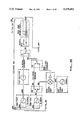
FIG. 1 shows one embodiment of a lightwave component analyzer, generally indicated by the numeral 10. As shown in FIGS. 1 and 2, the lightwave component analyzer 10 comprises an optical, or lightwave, test set 12 having an internal optical, or lightwave, receiver 16 and preferably having an internal optical, or lightwave, source 14. (See FIG. 2I.) The lightwave test set 12 also preferably comprises optical, or lightwave, test ports 121 and 122. All of the elements of the lightwave component analyzer 10, including the lightwave source 14 and the lightwave receiver 16, are extensively characterized so that high levels of precision in lightwave measurements are achieved when the lightwave component analyzer is calibrated. Preferably, the lightwave component analyzer 10 also comprises an electrical test set 18 for electrical measurements. The electrical test set 18 also preferably comprises electrical test ports 181 and 182.
The lightwave component analyzer 10 preferably comprises essentially a 20 GHz vector network analyzer, for example, an HP 8720A vector network analyzer available from Hewlett-Packard Company, Network Measurements Division, Santa Rosa, Calif., specifically tailored for lightwave measurements. An optical source (the lightwave source 14) and receiver (the lightwave receiver 16) are incorporated into the vector network analyzer by expanding an extant electrical test set (the electrical test set 18) to incorporate an optical test set (the lightwave test set 12) having optical test ports (the lightwave test ports 121 and 122) and preferably housing the optical source and receiver. Accordingly, the lightwave component analyzer 10 preferably includes both the electrical test set 18 and the lightwave test set 12 so that electrical, E/O, O/E, and optical calibrations and test measurements can be performed.
The electro-optical characteristics of the lightwave source 14 and the opto-electrical characteristics of the lightwave receiver 16 in a test setup have to be sensitive, stable, and repeatable. Also, their modulation bandwidths need to be wider than that of a device under test (DUT) connected to the lightwave test port(s) 121 and 122 and/or the electrical test port(s) 181 and 182. Most of the HP 8720A vector network analyzer is leveraged and reused for the analyzer and information processing portion, as well as the microwave electrical test set portion, of the lightwave component analyzer 10. Conversely, the lightwave test set 12 is added to the lightwave component analyzer 10. The lightwave source 14 and the lightwave receiver 16 incorporated into the lightwave test set 12 preferably have the following performance characteristics.
The lightwave component analyzer 10 provides an optical modulation signal source which preferably generates a high-stability, 1 Hz-resolution synthesized signal that can be swept from 130 MHz to 20 GHz. (See FIG. 2E) As shown in FIG. 2I, the lightwave source 14 preferably comprises a laser operating at 1300 nm followed by an optical isolator, a polarization controller, and a Mach-Zehnder interferometer optical modulator. The optical modulator is driven by a high power microwave signal. A modulation source in the HP 8720A vector network analyzer provides 130 MHz to 20 GHz signals to the RF port of the optical modulator to modulate the lightwave source 14.
The lightwave source 14 is preferably calibrated at the factory and in the field using an approach known as the two-tone technique. This technique is described in a poster paper by Roger Jungerman shown at OFC in New Orleans, La., during January, 1988. The two-tone technique takes advantage of the inherent nonlinearity in the transfer characteristic of the optical modulator. Two closely-spaced RF frequencies are applied to the RF port of the optical modulator. The optical beam carries a modulation component at the difference frequency. As the pair of frequencies is swept over the range of the optical modulator, the beat frequency amplitude traces out the frequency response of the modulator.
Modulation bandwidth of the lightwave source 14 is greater than 20 GHz, with better than +/-3 dB flatness. The intensity-modulated light signal from the lightwave source 14 is applied to either the lightwave test ports 121 and 122 of the lightwave test set 12 for calibration of the lightwave component analyzer 10 or to the lightwave test port 121 for a test measurement on a DUT.
The lightwave receiver 16 is a high-stability, high-resolution precision receiver with 50 dB dynamic range which allows measurements over a wide dynamic range and enables the lightwave component analyzer 10 to operate with an optical sensitivity of -50 dBm. The lightwave receiver 16 operates with single-mode optical fiber cable. Its optical detector is preferably a PIN photodiode. The lightwave receiver 16 has a modulation bandwidth that preferably extends to 20 GHz, with +/-3 dB flatness to 10 GHz, rolling off to -12 dB at 20 GHz. Minimum detectable optical signal (for modulations up to 20 GHz) is -50 dBm, and the typical optical dynamic range exceeds 40 dB. The 20 GHz modulation bandwidths of the lightwave source 14 and the lightwave receiver 16 provide ample margin for typical test measurements on a DUT.
The lightwave receiver 16 demodulates the modulated optical signal for processing in the lightwave component analyzer 10. The transmission and reflection characteristics of a DUT are then displayed, preferably on a cathode ray tube (CRT) 20 included in the lightwave component analyzer 10. The transmission and reflection data can be displayed either as a function of the RF modulation frequency or as a function of time or distance.
Considered in more detail, calibration and error-corrected test measurements for E/O and O/E devices in accordance with the invention involve switchably connecting the lightwave source 14 and the lightwave receiver 16 and the other portions of the lightwave component analyzer 10, as preferably shown in the schematic diagram of FIG. 2. As shown in FIG. 2I, the lightwave component analyzer 10 preferably incorporates the lightwave source 14 and the lightwave receiver 16 together with a switch matrix in the lightwave component analyzer. As shown in FIG. 2E, the lightwave component analyzer 10 includes a modulation source 22 which generates a 130 MHz. to 20 GHz electrical signal. As shown in FIG. 2H1, the electrical signal is preferably input to a power splitter 24 which initially feeds a selected portion of the electrical signal generated by the modulation source 22 to an electro-optical (E/O) transducer in the form of the lightwave source 14. Another portion of the electrical signal generated by the modulation source 22 is fed as a reference signal to one input port of a sampler 26 included in a tuned vector receiver 28 incorporated into the lightwave component analyzer 10, as shown in FIG. 2K.
There are several features of the hardware which distinguish the lightwave component analyzer 10 from both the HP 8720A vector network analyzer and the HP 8702A lightwave component measurement system. These features are the addition of a switch matrix comprising five additional RF switches in the electrical test set 18 and the lightwave test set 12 and the complete integration of the lightwave hardware into the lightwave component analyzer 10, preferably into the lightwave test set. The RF switches are preferably controlled through the normal user interface of the leveraged HP 8720A vector network analyzer and its resident microprocessor-based internal instrument controller in response to user selection of various calibration and test measurements.
Considered in more detail, the differences that exist between the electrical test set 18 and the microwave test set in the HP 8720A vector network analyzer are as follows. As shown in FIGS. 2H1 and 2K, RF switches S5, S6, and S7 are added. Also, a higher power microwave modulator and amplifier combination comprises the modulation source 22 to increase the RF power at the electrical test port 181 to +10 dBm (from -10 dBm in the HP 8720A vector network analyzer). Furthermore, a new ALC circuit is added to interface with the new microwave modulator in the new modulator-amplifier combination. (See FIG. 2A.) Additionally, the RF attenuator before the R channel input is increased to 40 dB to optimize the RF power into the R channel, as shown in FIGS. 2H1.
As shown in FIG. 2I, the optical source chain of the lightwave source 14 preferably comprises a CW semiconductor Fabry-Perot laser followed by an optical isolator, a polarization controller, and a Mach-Zehnder optical modulator. The polarization controller is needed to apply linearly polarized light at the appropriate angle to the input of the optical modulator.
The optical modulator is the device in the optical chain which superimposes the amplitude modulation envelope onto the CW laser light. The most important advantage of implementing the lightwave source 14 by means of an optical modulator instead of directly modulating the laser diode is that minimal fm chirp is generated with the optical modulator, which would otherwise occur when directly modulating a laser diode.
The optical isolator is present to stabilize the lightwave source 14 from back-reflected light which can be caused by any reflection interface in the measurement configuration, i.e., the optical modulator, optical connector interfaces, and test devices including optical launches into photodiodes, laser chip launches into fiber, etc.
An RF leveling loop is connected from the optical modulator to the microwave modulator-amplifier of the lightwave test set 12. The primary function of the RF leveling loop is to control the RF power drive into the optical modulator so that the modulated optical power is maximized and the modulation frequency response of the lightwave source 14 is optimally smooth.
As shown in FIGS. 1 and 2, the lightwave test set 12 preferably further comprises an additional optical, or lightwave, test port 123. Furthermore, the lightwave test set 12 further comprises an optical switch 32. If the optical switch 32 is positioned as shown in FIG. 2I, the internal Fabry-Perot laser provides light to be modulated. If a user desires light of a different optical frequency to be modulated, however, the user merely actuates the optical switch 32 to the other position shown in FIG. 2I and connects the output of an external laser (not shown) to the lightwave test port 123.
As shown in FIGS. 2H1, 2I, and 2K, the utilization of the six RF switches (S4 through S9) allows the routing of the RF input and output signals appropriately so that measurements of electrical, electro-optical, opto-electrical, and optical devices can be performed by a user more repeatably and easily. The RF switches S4, S5, S6, and S7 preferably reside in the electrical test set 18 and multiplex the HP 8720A vector network analyzer functions between RF and lightwave measurements. The RF switches S8 and S9 preferably reside in the lightwave test set 12. The RF switch S9 provides a way to monitor the RF power throughput of the optical modulator and indirectly a way to predict the modulated optical power as a function of frequency. The use of the RF output port of the optical modulator to obtain this signal avoids the need for a power tap preceding the modulator, allowing full power to be applied to the modulator. As shown in FIGS. 2E, 2H1, and 2I, the modulated RF signal is derived from the synthesized RF modulation source 22 through the RF switch S5 in series with an attenuation pad and a modulator-amplifier in the lightwave test set 12 and through the RF switch S8 to the RF drive port of the optical modulator.
FIG. 3 shows a table of RF switch settings for the lightwave component analyzer 10 configured to perform test measurements. The legend shown in FIG. 2Q facilitates an understanding of the connections which configure the switch matrix for performing these measurements.
FIG. 3 shows the RF switch configurations when measuring each device type, i.e., electrical (E/E), electro-optical (E/O), opto-electrical (O/E), and optical (O/O). With the switch matrix, measurements (E/E, E/O, O/E, and O/O) can be performed more accurately, repeatably, and easily. If different samplers are available, either the input and/or the output can be sampled. Accordingly, two test measurements can be performed simultaneously. A significant advantage which is a consequence of the internal RF switches is better measurement repeatability than if the RF connections were preformed manually. The repeatability of manual RF connections and disconnections is on the order of a few tenths of a decibel, as opposed to a few hundredths of a decibel repeatability for RF switches. Measurements require less time, as the number of steps in the measurement process is decreased by 40%.
Since the lightwave source 14 and the lightwave receiver 16 are integrated into the lightwave component analyzer 10, a unique calibration can be stored in the internal instrument memory. Accordingly, a user is allowed faster, more convenient, and easier calibrations and test measurements.
Calibration in connection with strictly electrical measurements is performed as in the HP 8720A vector network analyzer. Calibration in connection with electro-optical (E/O), opto-electrical (O/E), and optical measurements initially involves the lightwave component analyzer 10, lightwave source 14, and lightwave receiver 16. When the lightwave component analyzer 10 is used to characterize an E/O, O/E, or optical device, an initial calibration reference is established based on the known characteristics of the lightwave source 14 and the lightwave receiver 16.
Both the lightwave source 14 and the lightwave receiver 16 are earlier characterized in terms of their modulation (and demodulation) transfer characteristics (both absolute magnitude and phase) at the factory. The calibration data for accurate characterization of the lightwave source 14 and the lightwave receiver 16 are preferably measured at the time of construction or later maintenance and stored in EEPROMS in internal instrument memory. The lightwave component analyzer 10 incorporates firmware which can combine the calibration data arrays for use in subsequent measurements of fiber optic systems, subsystems, and associated component test measurements.
A user calibration measurement is then performed on the lightwave component analyzer 10 including the lightwave source 14 and/or the lightwave receiver 16, as well as the associated electrical and/or optical connections provided by the RF switch matrix, and error correction data are produced in the internal instrument controller by combining the factory and user calibration data, and the error correction data are then stored in the lightwave component analyzer internal instrument memory. The modulation (or demodulation) transfer characteristics are preferably given in terms of the responsivity magnitude and phase versus modulation frequency.
The internal instrument controller firmware of the lightwave component analyzer 10 incorporates coded instructions to perform the needed RF switch connections for the calibration process and while measuring the response characteristics of a DUT during desired test measurements. A calibration or measurement can be performed easily and quickly by user selection of the desired calibration or test measurement by actuation of a hard or soft key on the normal user interface of the leveraged HP 8720A vector network analyzer. The lightwave source 14 converts the electrical signal generated by the modulation source 22 to an optical signal. The optical signal produced by the lightwave source 14 is initially input to at least one opto-electrical electrical (O/E) transducer in the form of the lightwave receiver 16 during calibration. After calibration, a DUT in the form of an opto-electrical fiber optic system, subsystem, or associated component can have its input(s) connected to the lightwave test port(s) 121 and 122 of the lightwave test set 12 at the output(s) of the lightwave source 14 and its output(s) connected to the electrical test port(s) 181 and 182 of the electrical test set 18 so that the DUT can be tested, as shown in FIGS. 6B and 9.
The lightwave receiver 16 reconverts the received optical signal to an electrical signal. As shown in FIG. 2K, the electrical signal produced by the lightwave receiver 16 is fed to another sampler 30 of the tuned vector receiver 28 during calibration. After calibration, a DUT in the form of an electro-optical fiber optic system, subsystem, or associated component can have its input(s) connected to the electrical test ports 181 and 182 of the electrical test set 18 and its output(s) connected to the lightwave test port(s) 121 and 122 of the lightwave test set 12 at the input(s) of the lightwave receiver 16 so that the DUT can be tested, as shown in FIGS. 6A and 7.
Optical calibrations ad test measurements are performed by connections across the lightwave test ports 121 and 122 of the lightwave test set 12, as shown in FIGS. 6C and 11. Optical reflection (one port optical) calibrations and test measurements are also performed by connections to the lightwave test ports 121 and 122 of the lightwave test set 12, as shown in FIG. 13.
By including features of a conventional S-parameter calibration, the user can reduce uncertainty caused by imperfect electrical test port impedance match as will now be described. This improves the accuracy of E/O and O/E test measurements.
As shown in FIG. 4, a laser diode is an E/O device which can have an electrical input impedance of approximately 5 ohms, for example, which is significantly lower than the measurement system output impedance of 50 ohms at electrical test port 181. This poor impedance match results in standing waves between the RF source and the input port of the laser under test. A large systematic error is seen as a periodic ripple in the test measurement. The actual transmission frequency response does not contain this ripple. Electrical-source-to-E/O-device impedance mismatch calibration and error correction in accordance with the invention provide a more accurate test measurement by removing source match error.
The electrical-source-to-E/O-device calibration steps are as follows. Five steps are needed.
The first step is to measure a short on electrical test port 181. The second step is to measure an open on electrical test port 181. The third step is to measure a load on electrical test port 181. The data measured during these steps are used to calculate forward source match (Esf), forward reflection tracking (Erf), and forward directivity (Edf). The fourth step is to measure isolation, which is used as Exf. Finally, the fifth step is to measure electrical and optical through connections, which are used to calculate transmission tracking (Etf). The above five steps can be performed in any order.
After the five steps of this calibration are performed, the appropriate error correction data can be stored. Thereafter, the equation to error-correct E/O devices is: ##EQU3## where S21 meas is the measured transmission parameter containing systematic errors;
S21 actual is the corrected transmission parameter with source, match, cross-talk, and transmission tracking errors removed;
S11 meas is the measured, uncorrected electrical reflection parameter;
Edf is forward directivity;
Erf is forward reflection tracking;
Esf is forward source match;
Exf is isolation; and
Etf is transmission tracking.
Also, as shown in FIG. 5, a photodiode is an O/E device which can have an electrical output impedance of approximately 500 ohms, which is an impedance larger than the measurement system input impedance. This also results in a large systematic error which manifests itself as a ripple in the test measurement. O/E-device-to-electrical-receiver impedance mismatch calibration and error correction in accordance with the invention processes the measured data to remove load match errors to provide a more accurate test measurement.
The O/E-device-to-electrical receiver calibration steps are as follows. Nine steps are needed.
The first step is to measure a short on electrical test port 181. The second step is to measure an open on electrical test port 181. The third step is to measure a load on electrical test port 181. The data measured during these first three steps are used to calculate load match (Elf). The fourth step is to measure a short on electrical test port 182. The fifth step is to measure an open on electrical test port 182. The sixth step is to measure a load on electrical test port 182. The data measured during the fourth through sixth steps are used to calculate reverse source match (Esr), reverse reflection tracking (Err), and reverse directivity (Edr). The seventh step is to measure isolation, which is used as Exf. The eighth step is to measure an electrical through, which is used to calculate Elf. Finally, the ninth step is to measure electrical and optical through connections, which are used to calculate Etf. The above nine steps can be performed in any order.
After the nine steps of this calibration are performed, the appropriate error correction data can be stored. Thereafter, the equation to error-correct O/E devices is: ##EQU4## where S21 meas is the measured transmission parameter containing systematic errors;
S21 actual is the corrected transmission parameter with load match, cross-talk, and transmission tracking errors removed;
S22 meas is the measured, uncorrected electrical reflection parameter;
Edr is reverse directivity;
Err is reverse reflection tracking;
Esr is reverse source match;
Exf is isolation;
Elf is load match; and
Etf is transmission tracking.
These two forms of calibration and error correction can be thought of as subsets of full two-port, twelve-term error correction. Due to the nature of E/O devices, the reverse transmission is assumed to be zero. No correction is made for the impedance match at the optical port, and so the optical port match is assumed to be ideal. The full two-port error correction equations reduce to require only two measured parameters instead of four. Error correction of E/O devices requires five correction coefficients, while error correction of O/E devices requires six coefficients.
Edf, Edr, Erf, Err, Esf, Esr, Exf, Elf, and Etf can be calculated based on the preceding calibration measurements, as is well known. See, for example, Vector Measurements of High Frequency Networks. Hewlett-Packard Company Part No. 5958-0387 (Apr. 1, 1989), pages 3-5 to 3-16. The reflection coefficients may also be used for one-port error correction of S11 for E/O devices and S22 for O/E devices.
Accordingly, transmission measurements of E/O devices are corrected for source match errors, and transmission measurements of O/E devices are corrected for load match errors, in addition to frequency response and cross-talk error correction. Electrical-source-to-E/O-device impedance mismatch and O/E-device-to-electrical-receiver impedance mismatch calibration and error correction in accordance with the invention provide improved measurements of test devices with an electrical port having an impedance different from the impedance of the lightwave component analyzer 10.
The measurement of calibration standards and test device parameters is controlled by the lightwave component analyzer 10 as specified in the firmware. The calculation of error correction coefficients and the computation of the error correction algorithms using these coefficients is also contained in the analyzer firmware. The following is a copy of the firmware for the HP 8720A vector network analyzer internal instrument controller, which is executed to perform calibration and test measurements in accordance with the invention.
This module contains instructions to control measurement of calibration standards. This module also calculates error correction coefficients after the calibration standards are measured. ##SPC1##
Ease of use is achieved by implementing in RF switching many of the interconnections that would otherwise typically be manually performed by a user in a non-integrated test system, such as the HP 8702A lightwave component measurement system. With the integrated approach implemented in the lightwave component analyzer 10, a user is able to measure an electrical (E/E), electro-optical (E/O), opto-electrical (O/E), or optical (O/O) device easily. The measurement procedure is simpler than when performing the measurement with a non-integrated test system.
In addition to fewer steps to perform a measurement, the calibration process is more intuitive and logical. Calibration requires the connection of an RF cable and lightwave cable. To perform the measurement of an E/O or O/E device, a user simply disconnects the appropriate end of the RF and lightwave cable and connects the DUT.
The lightwave component analyzer 10 allows the measurement of the analog portion of the lightwave source 14 (transmitter) separately from the lightwave receiver 16, or visa versa. The measurements are fast and accurate, and the measurement process is convenient and easy to use. This provides the modulation/demodulation transfer measurement capability for assuring precise test measurements.
A DUT can then be measured when it is connected to the test ports of the electrical test set 18 and/or the lightwave test set 12 in a given measurement setup. The lightwave component analyzer 10 uses the error correction data when the electrical, E/O, O/E, or optical characteristics of the DUT are measured.
The test measurements on a DUT initially require the user to select a measurement. Then, the characteristics of the DUT are measured. Finally, the lightwave component analyzer 10 compensates the test measurements on the DUT using the error correction data. The lightwave component analyzer 10 facilitates user calibration and test measurements for E/O, O/E, and 0 Reflection (one port optical). Additionally, the firmware of the lightwave component analyzer 10 will set up the RF switches for E/E, O/O, and E Reflection (one port electrical).
The lightwave component analyzer 10 measures modulation (demodulation) bandwidth, modulation (demodulation) transfer functions, loss, delay, dispersion, and reflections of fiber optic system components, such as modulators, demodulators, optical fiber cables, and fiber components, based on frequency domain measurements. For optical components (such as optical fiber cable, couplers, and connectors), the lightwave component analyzer 10 can measure such parameters as modulation bandwidth, optical insertion loss, pulse dispersion, optical reflections, and length. Additionally, single and multiple reflections can be resolved in time and distance with very high resolution. This enables precise location of one or more discontinuities and measurement of optical fiber cable length.
Insofar as optical measurements are concerned, typical optical components are optical fiber cable, modulators, and passive devices, such as switches, splitters, combiners, and attenuators. The input and output signals for testing these devices are light, and the key parameters measured are attenuation versus modulation frequency, modulation bandwidth, delay, modal pulse dispersion, location of discontinuities, and length.
The dynamic range of optical measurements is typically greater than 40 dB. The two-event resolution of discontinuities measured in distance is less than 1 cm.
Additionally, the modulation transfer characteristics of electro-optical (E/O) transmitters and opto-electrical (O/E) receivers can also be precisely measured. For example, the responsivity of a PIN diode or laser diode can be measured, not only at one modulation frequency, but also as a function of modulation frequency from 130 MHz to 20 GHz.
Representative E/O devices are optical modulators and sources (such as laser diodes and LEDs). Examples of O/E devices are PIN or avalanche photodiode detectors in optical receivers. The key parameters for these devices are the same for both types, except that the independent and dependent variables are reversed; i.e., for E/O devices, optical power out is measured as a function of electrical (RF) drive, whereas RF power out as a function of optical drive is measured for O/E devices. Typical measurements for these devices are sensitivity (including the noise threshold/floor), as well as responsivity versus modulating frequency. Also, the lightwave component analyzer 10 can test reflection performance of electrical and optical device ports.
The RF (or electrical) elements of the fiber optic system under test can also be characterized utilizing the lightwave component analyzer 10. Examples of RF devices are amplifiers, filters, and cables used in a fiber optic system. The RF measurements include bandwidth, insertion loss/gain, phase, group delay, and complex impedance.
Electrical measurements can be performed on such RF components as amplifiers, filters, and cables, or a complete fiber optic repeater (comprising an optical transmitter, optical fiber cable, and optical receiver). Typical measurements include loss/gain versus modulation frequency, modulation bandwidth, modulation phase shift or phase delay, distortion (e.g., group delay or deviation from linear phase), complex impedance (magnitude and phase), and electrical length (including discontinuity location).
For example, one set of calibrated measurements is opto-electrical device sensitivity (responsivity) versus modulation frequency and modulation bandwidth measurements. The RF switch matrix is configured for an O/E user calibration, as indicated in FIGS. 2 and 3. The RF power into the lightwave source 14 is held at a constant power level [f(t)], and the modulation frequency is varied over some frequency range, f1 to f2.
The total modulation frequency response of the lightwave component analyzer 10 is measured. The measurement is operated upon by factory calibration data.
The resultant error correction data are then stored for later use. The calibration is now complete, and the next step is to measure an unknown device, i.e., the DUT.
To perform the measurement on the DUT, the DUT is connected diagonally to one electrical test port 181 or 182 of the electrical test set 18 and to one lightwave test port 121 or 122 of the lightwave test set 12. A display of receiver responsivity versus modulation frequency is then obtained. The information obtained from the display provided by the CRT 20 is the absolute receiver responsivity in amperes per watt (in a 50-ohm impedance system), the modulation bandwidth of the DUT, and the responsivity variation from a constant level over the modulation frequency range (or responsivity variation over modulation frequency).
The corresponding measurements can be performed for sources or electro-optical devices. For the source case, the responsivity is in terms of watts per ampere; other comments made for the receiver measurements also apply for these measurements.
Considered in more detail, one parameter set is the demodulation bandwidth measurement for a demodulator (or receiver). The lightwave (or carrier) frequency is fixed, for example, at 1300 nm, and the modulation frequency is varied over some frequency range, such as 130 MHz to 20 GHz, by the modulation source 22. The lightwave source 14 outputs an amplitude modulated lightwave, where the lightwave is a constant frequency, but the modulation frequency varies over some frequency range.
The demodulator (or receiver), typically a photodiode and pre-amp, strips away the carrier frequency and recovers the modulated signal, g(w). The lightwave component analyzer 10 forms the ratio of g/f for each modulation frequency and operates on that ratio (g/f) and displays the transfer characteristic versus modulation frequency.
The foregoing description is offered primarily for purposes of illustration. Various modifications can be made. For example, an HP Series 217 instrument controller and an HP 3488 switch controller can be provided to configure the RF switch matrix. The HP Series 217 instrument controller software incorporates coded instructions to perform the needed switch connections for the calibration process and while measuring the response characteristics of a DUT during desired test measurements. A calibration or test measurement can be performed easily and quickly by user selection of the desired calibration or measurement by actuation of a key on the keyboard of the HP Series 217 instrument controller. It will be readily apparent to those skilled in the art that numerous other modifications and variations not mentioned above can still be made without departing from the spirit and scope of the invention as claimed below.