US5170154A - Bus structure and method for compiling pixel data with priorities - Google Patents
Bus structure and method for compiling pixel data with priorities Download PDFInfo
- Publication number
- US5170154A US5170154A US07/547,024 US54702490A US5170154A US 5170154 A US5170154 A US 5170154A US 54702490 A US54702490 A US 54702490A US 5170154 A US5170154 A US 5170154A
- Authority
- US
- United States
- Prior art keywords
- pixel data
- pair
- inputs
- priority
- data
- Prior art date
- Legal status (The legal status is an assumption and is not a legal conclusion. Google has not performed a legal analysis and makes no representation as to the accuracy of the status listed.)
- Expired - Lifetime
Links
Images


Classifications
-
- G—PHYSICS
- G09—EDUCATION; CRYPTOGRAPHY; DISPLAY; ADVERTISING; SEALS
- G09G—ARRANGEMENTS OR CIRCUITS FOR CONTROL OF INDICATING DEVICES USING STATIC MEANS TO PRESENT VARIABLE INFORMATION
- G09G5/00—Control arrangements or circuits for visual indicators common to cathode-ray tube indicators and other visual indicators
- G09G5/36—Control arrangements or circuits for visual indicators common to cathode-ray tube indicators and other visual indicators characterised by the display of a graphic pattern, e.g. using an all-points-addressable [APA] memory
- G09G5/39—Control of the bit-mapped memory
- G09G5/395—Arrangements specially adapted for transferring the contents of the bit-mapped memory to the screen
- G09G5/397—Arrangements specially adapted for transferring the contents of two or more bit-mapped memories to the screen simultaneously, e.g. for mixing or overlay
-
- G—PHYSICS
- G09—EDUCATION; CRYPTOGRAPHY; DISPLAY; ADVERTISING; SEALS
- G09G—ARRANGEMENTS OR CIRCUITS FOR CONTROL OF INDICATING DEVICES USING STATIC MEANS TO PRESENT VARIABLE INFORMATION
- G09G2340/00—Aspects of display data processing
- G09G2340/10—Mixing of images, i.e. displayed pixel being the result of an operation, e.g. adding, on the corresponding input pixels
-
- G—PHYSICS
- G09—EDUCATION; CRYPTOGRAPHY; DISPLAY; ADVERTISING; SEALS
- G09G—ARRANGEMENTS OR CIRCUITS FOR CONTROL OF INDICATING DEVICES USING STATIC MEANS TO PRESENT VARIABLE INFORMATION
- G09G5/00—Control arrangements or circuits for visual indicators common to cathode-ray tube indicators and other visual indicators
- G09G5/02—Control arrangements or circuits for visual indicators common to cathode-ray tube indicators and other visual indicators characterised by the way in which colour is displayed
- G09G5/022—Control arrangements or circuits for visual indicators common to cathode-ray tube indicators and other visual indicators characterised by the way in which colour is displayed using memory planes
Definitions
- This invention relates to bus structures for computers and more particularly to the structure by which blocks of pixel data for a raster-type display can be compiled in real time from multiple memory planes with associated priorities for the blocks of pixel data from selected memory planes.
- images which are to be displayed in a raster-type display are controlled by pixel data that is retrieved in real time from bit-mapped locations in a plurality of memory planes (or, in a plurality of sections of a memory plane).
- the blocks of pixel data associated with separate bit-mapped images may be accorded selected priorities in order to compile overlapping images on the display in accordance with selected near-far orientation priorities.
- an image of a house may be displayed in overlapping priority relative to the image of a tree which in turn may be displayed in overlapping priority relative to the displayed image of a mountain, and so on, where the image of each displayed object may be compiled from pixel data that is conveniently bit-mapped into individual memory planes.
- priorities for each object can be altered to modify the overlapping near-far orientations of the objects in a composite display.
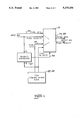
- FIG. 1 is a schematic diagram of a conventional structure for combining multiple sources of pixel data
- FIG. 2 is a pictorial and schematic diagram of the illustrated embodiment of the present invention.
- FIG. 3 is a graph illustrating the timing of events in the operation of the embodiment of FIG. 2;
- FIGS. 4 (a)-(h) are pictorial illustrations of displayable images that are bit-mapped in memory planes or equivalently available in real time;
- FIG. 5 is a block diagram of one embodiment of bus operators for compiling pixel data along the bus structure of the present invention
- FIGS. 6 and 7 are pictorial representations of pixel data from different memory planes in different data formats.
- FIG. 8 is a pictorial representation of pixel data with associated priority value.
- FIG. 1 there is shown a simplified block schematic diagram of conventional circuitry commonly used to compile real time pixel data from multiple memory planes 9-12, each associated with a displayable image, into a horizontal scan line of data for application to and control of a raster type display screen 13.
- Selective accessing of pixel data from a memory plane 9-12 for a particular displayable image is under control of data requests 15 (typically, address information per plane) provided by synchronizing generator 17.
- the accessed pixel data is compiled in real time in a display processor 19 which may include a multiplexer or an OR gate and a digital to analog converter for producing display-controlling signals 21 that provide the desired display of the images in memories 9-12 on display screen 13.
- the pixel data associated with displayable images stored in bit-mapped memory planes 23-26 are accumulated or cascaded along a pixel data bus 22 in a synchronous daisy-chain configuration for compiling pixel data in real time per displayable line of data applied to raster-type display 27.
- Each memory plane 23-26 may have an image or images bit-mapped therein at selected addresses for retrieval and application to the bus structure in successive clock intervals under the control of synchronous generator 29.
- the pixel data that is retrieved from each memory plane 23-26 is combined on the bus 22 via display processor or operator 31-34, as described in detail later herein.
- each memory plane 23-26 and associated operator or data processor 31-34 required one clock interval for access and transfer of stored pixel data from memory to the bus structure 22, then with reference to the time when signals 35 are required to be supplied to the display screen 27, each memory plane 23-26 and associated operator 31-34 preceding the output 35 of the bus structure 22 requires address and data requests from the synchronous generator 29 at progressively earlier or advanced intervals.
- memory plane 26 requires data request control signals 37 one interval earlier than the output 35 is required
- memory plane 25 requires data request control signals 39 two intervals earlier
- memory plane 24 requires data request control signals 41 three intervals earlier, and so on for all N number of memory planes 23-26 and associated operators 31-34 with bus structure 22.
- Such uniform data transfer interval may be encountered in memory planes 23-26, which may be actually only different segments of a single, larger memory plane.
- several different types of memory planes having different access and retrieval delay intervals can be cascaded along the bus structure 22 without limitation beyond the requirement for sufficiently advanced data request control signals 37-43 being supplied in advance to facilitate all data transfers onto the bus in real time for complete compilation when required at output 35 for application to display screen 27 as a complete horizontal scan line of pixel data.
- a particular block of pixel data 35 may only be needed at a particular pixel count along the display positions of a horizontal scan line on the display screen 27.
- the pixel data retrieved from the memory planes 23-26 may be "pipelined" in real time along the bus structure 22 to arrive at the output 35 at a particular pixel count interval of the display screen 27.
- FIG. 3 there is shown an accumulation of advanced data requests to each memory plane that are determined by the summation of different data transfer delays of all succeeding memory planes along the bus structure 22 to the output 35.
- data retrievals and transfers from the memory planes 23-26 to and along the bus structure 22 proceed at the pixel clock rate (typically 15-30 MHz) determined by the raster-type display screen 27.
- a register in each processor 31-34 may store the requisite delay for access and transfer to the bus structure 22 of pixel data stored in the associated memory plane 23-26, and generator 29 need only respond to the data in such registers to determine the cumulative lead intervals by which to initiate the data requests 37-43.
- the pictorial equivalent of blocks of pixel data as bit-mapped into each memory plane 23-26.
- the pixel data for each stored image has associated therewith per pixel one or more priority bits to indicate different priority zones, to associate priority with pixel position, to associate priority with color, and to associate priority with region.
- the pixel data for each pixel associated with the image of, say, a house 51 includes at least one bit of data that designates the separation between priority regions (house 51 v. background 53) and that designates the level of priority assigned to each region (higher numbers designate nearer field or closer positional orientation when displayed), in addition to RGB data, and the like.
- This pixel data may be stored in any of the memory planes 23-26 along the bus structure without loss of control of assigned priorities for reasons as later described herein.
- the pixel data associated with the FIG. 55 in FIG. 4(b) may include bits designating priority zones 55 and 57 and priority level (e.g., 5), in addition to RGB data, and such data may be stored in any other memory 23-26 connected in the bus structure 22.
- the pixel data associated with other displayable images, as illustrated in FIGS. 4(c) and (d) include bits of data to designate priority zones and priority levels, in addition to RGB data, and the like.
- the priority data 36, 38, 40, 42 associated with each pixel of a stored image is accessed and transferred 44, 46, 48, 50 along the bus structure 22 from each memory plane 23-26 in order to determine at each operator 31-34 whether a block of pixel data of lower priority will be exchanged for a block of
- FIGS. 4(e)-(h) pictorially illustrate the equivalent displays of all compiled pixel data (over all pixel counts for all horizontal scan lines for one frame of display) available at the outputs of each of the display processors or operators 31-34, delayed successively in time per position of the associated memory plane along the bus structure 22.
- pixel data associated with the house is assigned higher priority level than the background pixel data, so the equivalent display based on pixel data available at the output of operator 31 is as illustrated in FIG. 4(e).
- the combined pixel data with associated priority zones and levels that are compiled from the pixel data transferred along the bus structure 22 from memory plane 23, and accessed from memory plane 24 yields the equivalent display illustrated in FIG. 4(f) (for all pixel data for all horizontal scan lines for one frame of display).
- the pixels for the FIG. 55 overlay or replace the pixels for the house which, in turn, overlay or replace the background pixels 53 and 57.
- the compiled pixel data available at the output of operator 33 yields the equivalent display (under the conditions referred to above), as illustrated in FIG. 4(g).
- the pixels for the FIG. 55 overlay the pixels for the tree and the house and backgrounds, and the pixels for the tree overlay the pixels for the house and backgrounds, and the pixels for the house overlay the backgrounds and the lower background 61 overlays the upper background 53, 57.
- FIG. 4(d) are compiled with pixel data and priority values transferred along the bus structure 22 from preceding memory planes 23-25 to yield the equivalent the display (under the conditions referred to above) as illustrated in FIG. 4(h).
- Such compiled pixel data constitutes the pixel data at the output 35 of the bus structure 22 that drives the display 27 at all pixel counts along all horizontal scan lines to yield the display frame illustrated in FIG. 4(h) including all of the stored images displayed in overlapping (and obliterating) orientations.
- pixel data for all pixels along a given horizontal scan line are compiled as a string of blocks of pixel data, wherein in the pixel data for a given pixel count from two or more memory planes (i.e., overlapping relationship of displayable objects) is evaluated for priority values, and the pixel data for a given pixel count having a certain lower priority value is exchanged for the pixel data for the same pixel count having a corresponding higher priority value.
- Conflicts in priority values e.g., equality in zone or level
- pixel data associated wi backgrounds at conflicting priority levels for different displayable objects may be resolved exchanging pixel data including light blue information (e.g., sky) for pixel data including dark blue information (e.g., water).
- light blue information e.g., sky
- dark blue information e.g., water
- Each such operator includes a multiplexer 71 having pixel data inputs 73, 75 for receiving pixel data on the bus structure 22 and from the associated memory plane for connecting one of the set of inputs to the output 77 in response to a priority control input 79.
- a comparator 81 is coupled to receive the priority data A associated with pixel data on the bus structure 22, and the priority data B associated with the pixel data from a memory plane to supply a control signal 79 to the multiplexer 71.
- the multiplexer 71 conducts to the output thereof the pixel data (and associated priority data) on the bus or from the memory plane that has the highest priority.
- Such pixel data with associated priority data thus propagates along the bus structure in real time until exchanged for pixel data having higher priority values, with the result that the pixel data with the associated highest priority data is presented at the output 35 to drive the display screen 27.
- FIG. 6 there is shown a pictorial representation of pixel data in three different formats from three different memory planes 23-26.
- different types of memory planes having different data access and transfer delays and also having different formats for storing pixel data can be connected in cascade or daisy-chain bus configuration, as illustrated in FIG. 2.
- the bus structure 22 is capable of handling 8-bit (maximum) pixel data
- memory planes 23-26 storing pixel data in format containing fewer bits can also operate compatibly on the bus in accordance with another aspect of the present invention. It should be noted that it is not sufficient to add non-significant zeros to pixel data of fewer bits in order to fill 8-bit data format.
- the subset block of pixel data 81 (say, in 3-bit format) is replicated as a block of data within the next less significant bit positions 81, with the remainder of the 8-bit format replicated from the most significant data bits 83 to yield substantially the same fraction of range represented by the different N-bit data formats.
- 5-bit data format 85 may be converted to 8-bit data format 87, and to 3-bit data format 89, as described above, in accordance with the following algorithm:
- substantially the entire range of values in a reference data format can be covered with substantial linearity over the range of data in the format from which the pixel data is converted.
- the present bus structure facilitates the compilation in real time of the pixel data required to display multiple overlapping objects on a raster-type display.
- the present bus structure resolves priorities for pixel data of overlapping objects independent of orientation of a memory plane containing the pixel data for a displayable object along the cascaded bus structure.
Abstract
Description
R.sub.x =N.sub.(x)mood in (Eq. 1)
Claims (2)
Priority Applications (1)
| Application Number | Priority Date | Filing Date | Title |
|---|---|---|---|
| US07/547,024 US5170154A (en) | 1990-06-29 | 1990-06-29 | Bus structure and method for compiling pixel data with priorities |
Applications Claiming Priority (1)
| Application Number | Priority Date | Filing Date | Title |
|---|---|---|---|
| US07/547,024 US5170154A (en) | 1990-06-29 | 1990-06-29 | Bus structure and method for compiling pixel data with priorities |
Publications (1)
| Publication Number | Publication Date |
|---|---|
| US5170154A true US5170154A (en) | 1992-12-08 |
Family
ID=24183033
Family Applications (1)
| Application Number | Title | Priority Date | Filing Date |
|---|---|---|---|
| US07/547,024 Expired - Lifetime US5170154A (en) | 1990-06-29 | 1990-06-29 | Bus structure and method for compiling pixel data with priorities |
Country Status (1)
| Country | Link |
|---|---|
| US (1) | US5170154A (en) |
Cited By (9)
| Publication number | Priority date | Publication date | Assignee | Title |
|---|---|---|---|---|
| EP0539822A2 (en) * | 1991-10-31 | 1993-05-05 | International Business Machines Corporation | Video insertion processing system |
| EP0590785A2 (en) * | 1992-09-30 | 1994-04-06 | Hudson Soft Co., Ltd. | Processing apparatus for sound and image data |
| EP0690430A3 (en) * | 1994-06-02 | 1996-07-03 | Accelerix Ltd | Single chip frame buffer and graphics accelerator |
| US5542041A (en) * | 1992-12-07 | 1996-07-30 | Brooktree Corporation | Apparatus for, and methods of, providing a universal format of pixels and for scaling fields in the pixels |
| FR2747809A1 (en) * | 1996-04-19 | 1997-10-24 | Mitsubishi Elec Semiconductor | IMAGE VIEWING CONTROL DEVICE |
| US5752010A (en) * | 1993-09-10 | 1998-05-12 | At&T Global Information Solutions Company | Dual-mode graphics controller with preemptive video access |
| US6041010A (en) * | 1994-06-20 | 2000-03-21 | Neomagic Corporation | Graphics controller integrated circuit without memory interface pins and associated power dissipation |
| US6449009B1 (en) * | 1994-05-19 | 2002-09-10 | Pandora International Limited | Image transfer method for telecine |
| US20060227145A1 (en) * | 2005-04-06 | 2006-10-12 | Raymond Chow | Graphics controller having a single display interface for two or more displays |
Citations (4)
| Publication number | Priority date | Publication date | Assignee | Title |
|---|---|---|---|---|
| US4233601A (en) * | 1977-04-04 | 1980-11-11 | International Computers Limited | Display system |
| US4864289A (en) * | 1984-04-13 | 1989-09-05 | Ascii Corporation | Video display control system for animation pattern image |
| US4951229A (en) * | 1988-07-22 | 1990-08-21 | International Business Machines Corporation | Apparatus and method for managing multiple images in a graphic display system |
| US4992781A (en) * | 1987-07-17 | 1991-02-12 | Sharp Kabushiki Kaisha | Image synthesizer |
-
1990
- 1990-06-29 US US07/547,024 patent/US5170154A/en not_active Expired - Lifetime
Patent Citations (4)
| Publication number | Priority date | Publication date | Assignee | Title |
|---|---|---|---|---|
| US4233601A (en) * | 1977-04-04 | 1980-11-11 | International Computers Limited | Display system |
| US4864289A (en) * | 1984-04-13 | 1989-09-05 | Ascii Corporation | Video display control system for animation pattern image |
| US4992781A (en) * | 1987-07-17 | 1991-02-12 | Sharp Kabushiki Kaisha | Image synthesizer |
| US4951229A (en) * | 1988-07-22 | 1990-08-21 | International Business Machines Corporation | Apparatus and method for managing multiple images in a graphic display system |
Non-Patent Citations (8)
| Title |
|---|
| "DVA-4000/ISA" data sheet, Video Logic 1989. |
| DVA 4000/ISA data sheet, Video Logic 1989. * |
| Guglielmo, Connie and Battle, John, "RasterOps Cut Multimedia Costs," MacWeek, pp. 1 and 9, Feb. 6, 1990. |
| Guglielmo, Connie and Battle, John, RasterOps Cut Multimedia Costs, MacWeek, pp. 1 and 9, Feb. 6, 1990. * |
| Markoff, John, "Personal Computers May Soon Add TV's Beauty," New York Times, pp. C1 and C5, Sep. 12, 1989. |
| Markoff, John, Personal Computers May Soon Add TV s Beauty, New York Times, pp. C1 and C5, Sep. 12, 1989. * |
| Visual Communications, Inc., "D.FACTO," May 1989 pp. 1-20. |
| Visual Communications, Inc., D.FACTO, May 1989 pp. 1 20. * |
Cited By (24)
| Publication number | Priority date | Publication date | Assignee | Title |
|---|---|---|---|---|
| EP0539822A2 (en) * | 1991-10-31 | 1993-05-05 | International Business Machines Corporation | Video insertion processing system |
| EP0539822A3 (en) * | 1991-10-31 | 1993-10-13 | International Business Machines Corporation | Video insertion processing system |
| US5630105A (en) * | 1992-09-30 | 1997-05-13 | Hudson Soft Co., Ltd. | Multimedia system for processing a variety of images together with sound |
| EP0590785A3 (en) * | 1992-09-30 | 1995-08-09 | Hudson Soft Co Ltd | Processing apparatus for sound and image data. |
| EP0590785A2 (en) * | 1992-09-30 | 1994-04-06 | Hudson Soft Co., Ltd. | Processing apparatus for sound and image data |
| US5542041A (en) * | 1992-12-07 | 1996-07-30 | Brooktree Corporation | Apparatus for, and methods of, providing a universal format of pixels and for scaling fields in the pixels |
| US5752010A (en) * | 1993-09-10 | 1998-05-12 | At&T Global Information Solutions Company | Dual-mode graphics controller with preemptive video access |
| US6449009B1 (en) * | 1994-05-19 | 2002-09-10 | Pandora International Limited | Image transfer method for telecine |
| EP0690430A3 (en) * | 1994-06-02 | 1996-07-03 | Accelerix Ltd | Single chip frame buffer and graphics accelerator |
| USRE37944E1 (en) | 1994-06-02 | 2002-12-31 | 3612821 Canada Inc. | Single chip frame buffer and graphics accelerator |
| USRE44589E1 (en) | 1994-06-02 | 2013-11-12 | Mosaid Technologies Incorporated | Single chip frame buffer and graphics accelerator |
| US5694143A (en) * | 1994-06-02 | 1997-12-02 | Accelerix Limited | Single chip frame buffer and graphics accelerator |
| USRE41565E1 (en) | 1994-06-02 | 2010-08-24 | Mosaid Technologies Incorporated | Single chip frame buffer and graphics accelerator |
| USRE40326E1 (en) | 1994-06-02 | 2008-05-20 | Mosaid Technologies Incorporated | Single chip frame buffer and graphics accelerator |
| US6356497B1 (en) | 1994-06-20 | 2002-03-12 | Neomagic Corporation | Graphics controller integrated circuit without memory interface |
| US6771532B2 (en) | 1994-06-20 | 2004-08-03 | Neomagic Corporation | Graphics controller integrated circuit without memory interface |
| US20040179015A1 (en) * | 1994-06-20 | 2004-09-16 | Neomagic Corporation | Graphics controller integrated circuit without memory interface |
| US6920077B2 (en) | 1994-06-20 | 2005-07-19 | Neomagic Corporation | Graphics controller integrated circuit without memory interface |
| US7106619B2 (en) | 1994-06-20 | 2006-09-12 | Neomagic Corporation | Graphics controller integrated circuit without memory interface |
| US20060208764A1 (en) * | 1994-06-20 | 2006-09-21 | Puar Deepraj S | Graphics Controller Integrated Circuit without Memory Interface |
| US6041010A (en) * | 1994-06-20 | 2000-03-21 | Neomagic Corporation | Graphics controller integrated circuit without memory interface pins and associated power dissipation |
| US5953019A (en) * | 1996-04-19 | 1999-09-14 | Mitsubishi Electric Semiconductor Software Co., Ltd. | Image display controlling apparatus |
| FR2747809A1 (en) * | 1996-04-19 | 1997-10-24 | Mitsubishi Elec Semiconductor | IMAGE VIEWING CONTROL DEVICE |
| US20060227145A1 (en) * | 2005-04-06 | 2006-10-12 | Raymond Chow | Graphics controller having a single display interface for two or more displays |
Similar Documents
| Publication | Publication Date | Title |
|---|---|---|
| US5293540A (en) | Method and apparatus for merging independently generated internal video with external video | |
| US4121283A (en) | Interface device for encoding a digital image for a CRT display | |
| US5315692A (en) | Multiple object pipeline display system | |
| EP0166966B1 (en) | Video display controller | |
| US4823120A (en) | Enhanced video graphics controller | |
| EP0128051B1 (en) | Video display system | |
| EP0197413B1 (en) | Frame buffer memory | |
| US5539464A (en) | Apparatus, systems and methods for generating displays from dual source composite data streams | |
| US5481319A (en) | Motion detection method and apparatus | |
| JP3385135B2 (en) | On-screen display device | |
| US5714974A (en) | Dithering method and circuit using dithering matrix rotation | |
| US4586036A (en) | Graphics display systems | |
| KR950014980B1 (en) | Video processing and data inserting system | |
| US6466224B1 (en) | Image data composition and display apparatus | |
| EP0201210B1 (en) | Video display system | |
| US4791580A (en) | Display processor updating its color map memories from the serial output port of a video random-access memory | |
| US5170154A (en) | Bus structure and method for compiling pixel data with priorities | |
| US4866524A (en) | Television picture overlay management device | |
| GB2145308A (en) | Display selection in a raster scan display system | |
| AU650139B2 (en) | Method and apparatus for generating video signals | |
| US5943097A (en) | Image processing means for processing image signals of different signal formats | |
| US5541665A (en) | Image processing apparatus with change over of clock signals | |
| US4614941A (en) | Raster-scan/calligraphic combined display system for high speed processing of flight simulation data | |
| US5608466A (en) | Color picture synthesizer producing an accurate chroma-key despite variations in the intensity level of a designated color signal | |
| JPH03206492A (en) | Window priority encoder |
Legal Events
| Date | Code | Title | Description |
|---|---|---|---|
| AS | Assignment |
Owner name: RADIUS INC. A CORP OF CA, CALIFORNIA Free format text: ASSIGNMENT OF ASSIGNORS INTEREST.;ASSIGNORS:MANTOPOULOS, THIERRY G.;QUINARD, FABRICE M.;REEL/FRAME:005367/0305 Effective date: 19900629 |
|
| STCF | Information on status: patent grant |
Free format text: PATENTED CASE |
|
| CC | Certificate of correction | ||
| AS | Assignment |
Owner name: IBM CREDIT CORPORATION, CONNECTICUT Free format text: SECURITY AGREEMENT;ASSIGNOR:RADIUS, INC.;REEL/FRAME:007803/0339 Effective date: 19960125 |
|
| REMI | Maintenance fee reminder mailed | ||
| FPAY | Fee payment |
Year of fee payment: 4 |
|
| SULP | Surcharge for late payment | ||
| FEPP | Fee payment procedure |
Free format text: PAYOR NUMBER ASSIGNED (ORIGINAL EVENT CODE: ASPN); ENTITY STATUS OF PATENT OWNER: LARGE ENTITY |
|
| FEPP | Fee payment procedure |
Free format text: PAT HLDR NO LONGER CLAIMS SMALL ENT STAT AS SMALL BUSINESS (ORIGINAL EVENT CODE: LSM2); ENTITY STATUS OF PATENT OWNER: LARGE ENTITY |
|
| FPAY | Fee payment |
Year of fee payment: 8 |
|
| AS | Assignment |
Owner name: DIGITAL ORIGIN, INC., CALIFORNIA Free format text: CHANGE OF NAME;ASSIGNOR:RADIUS, INC.;REEL/FRAME:014515/0062 Effective date: 19990226 |
|
| FPAY | Fee payment |
Year of fee payment: 12 |
|
| AS | Assignment |
Owner name: AUTODESK, INC., CALIFORNIA Free format text: ASSIGNMENT OF ASSIGNORS INTEREST;ASSIGNOR:DIGITAL ORIGIN, INC.;REEL/FRAME:014718/0388 Effective date: 20040607 |