US5157627A - Method and apparatus for setting desired signal level on storage element - Google Patents
Method and apparatus for setting desired signal level on storage element Download PDFInfo
- Publication number
- US5157627A US5157627A US07/554,313 US55431390A US5157627A US 5157627 A US5157627 A US 5157627A US 55431390 A US55431390 A US 55431390A US 5157627 A US5157627 A US 5157627A
- Authority
- US
- United States
- Prior art keywords
- state
- storage element
- signal
- select storage
- defining
- Prior art date
- Legal status (The legal status is an assumption and is not a legal conclusion. Google has not performed a legal analysis and makes no representation as to the accuracy of the status listed.)
- Expired - Fee Related
Links
- 238000000034 method Methods 0.000 title claims description 38
- 238000012360 testing method Methods 0.000 claims abstract description 80
- 239000011159 matrix material Substances 0.000 claims abstract description 15
- 239000000523 sample Substances 0.000 claims description 40
- 238000012544 monitoring process Methods 0.000 claims description 4
- 230000008878 coupling Effects 0.000 claims 10
- 238000010168 coupling process Methods 0.000 claims 10
- 238000005859 coupling reaction Methods 0.000 claims 10
- 230000003247 decreasing effect Effects 0.000 claims 1
- 238000010586 diagram Methods 0.000 description 12
- 238000013459 approach Methods 0.000 description 7
- 238000013461 design Methods 0.000 description 5
- 230000005540 biological transmission Effects 0.000 description 3
- 230000008901 benefit Effects 0.000 description 2
- 238000005516 engineering process Methods 0.000 description 2
- 230000005284 excitation Effects 0.000 description 2
- 230000003213 activating effect Effects 0.000 description 1
- 230000004075 alteration Effects 0.000 description 1
- 210000004027 cell Anatomy 0.000 description 1
- 230000000694 effects Effects 0.000 description 1
- 230000005669 field effect Effects 0.000 description 1
- 239000004065 semiconductor Substances 0.000 description 1
- 210000000352 storage cell Anatomy 0.000 description 1
- 238000006467 substitution reaction Methods 0.000 description 1
Images


Classifications
-
- G—PHYSICS
- G11—INFORMATION STORAGE
- G11C—STATIC STORES
- G11C11/00—Digital stores characterised by the use of particular electric or magnetic storage elements; Storage elements therefor
- G11C11/21—Digital stores characterised by the use of particular electric or magnetic storage elements; Storage elements therefor using electric elements
- G11C11/34—Digital stores characterised by the use of particular electric or magnetic storage elements; Storage elements therefor using electric elements using semiconductor devices
- G11C11/40—Digital stores characterised by the use of particular electric or magnetic storage elements; Storage elements therefor using electric elements using semiconductor devices using transistors
- G11C11/401—Digital stores characterised by the use of particular electric or magnetic storage elements; Storage elements therefor using electric elements using semiconductor devices using transistors forming cells needing refreshing or charge regeneration, i.e. dynamic cells
- G11C11/4063—Auxiliary circuits, e.g. for addressing, decoding, driving, writing, sensing or timing
- G11C11/407—Auxiliary circuits, e.g. for addressing, decoding, driving, writing, sensing or timing for memory cells of the field-effect type
-
- G—PHYSICS
- G01—MEASURING; TESTING
- G01R—MEASURING ELECTRIC VARIABLES; MEASURING MAGNETIC VARIABLES
- G01R31/00—Arrangements for testing electric properties; Arrangements for locating electric faults; Arrangements for electrical testing characterised by what is being tested not provided for elsewhere
- G01R31/28—Testing of electronic circuits, e.g. by signal tracer
- G01R31/317—Testing of digital circuits
- G01R31/3181—Functional testing
- G01R31/3185—Reconfiguring for testing, e.g. LSSD, partitioning
-
- G—PHYSICS
- G11—INFORMATION STORAGE
- G11C—STATIC STORES
- G11C29/00—Checking stores for correct operation ; Subsequent repair; Testing stores during standby or offline operation
- G11C29/04—Detection or location of defective memory elements, e.g. cell constructio details, timing of test signals
- G11C29/08—Functional testing, e.g. testing during refresh, power-on self testing [POST] or distributed testing
-
- G—PHYSICS
- G11—INFORMATION STORAGE
- G11C—STATIC STORES
- G11C7/00—Arrangements for writing information into, or reading information out from, a digital store
- G11C7/20—Memory cell initialisation circuits, e.g. when powering up or down, memory clear, latent image memory
Definitions
- This invention relates to an apparatus and method for setting desired signal levels at select storage elements of an integrated circuit. More particularly, this invention relates to an apparatus and method for setting the desired signal levels at select storage elements by overpowering the logic state that would otherwise occur. Further, this invention relates to an apparatus and method for setting the desired signal levels without supplying the desired levels through primary input pins of the integrated circuit, but rather through a matrix of predefined test points.
- the integrated circuit is designed to tie the select storage elements to one or more shift register chains.
- the shift registers can thereafter be loaded through test contacts or through the primary input pins during a test, enabling the desired logic states to be loaded to the select storage elements.
- the conventional SCAN approaches multiplex the input to the storage element so that during testing, the test circuitry generates the input signal, whereas during normal operation the normal integrated circuit logic generates the input signal.
- a functionally independent, internal grid-based structure for an integrated circuit is disclosed enabling testing of complex integrated circuits.
- a grid-structure 10 on an integrated circuit 11 is formed of individually accessible probe lines 12 and sense/control lines 14 with electronic switches 16 at the crossings.
- a probe line 12 is coupled to a switch 16 for defining the switch "ON” or "OFF” state.
- One end of the switch 16 is coupled to a test point 18 of the integrated circuit 11, while the other end is coupled to a sense/control line 14 for monitoring a signal from the test point 18.
- Activating a select switch 16 through a corresponding probe line 12 enables monitoring or exciting a test point.
- the integrated circuit includes primary input pins 19, probe line contacts 20 and sense line contacts 21.
- the test points 18 are coupled to the input line or output line of a corresponding gate G.
- the grid structure described above is used for observing signals at the test points 18.
- the switches 16 coupled to the test points 18 have a high impedance so as to provide less current drive than the logic gates G. As a result, the switch lines do not alter or disturb the internal signals of the integrated circuit 11 during observation.
- Difficulties to be overcome in using such a grid structure to impose a desired signal level on an output line of an internal circuit include the relatively low current drive of the switches 16 relative to the gates G.
- the benefit given by the lower drive current for observing the test signals is a detriment in writing to gate output lines.
- the drive current may be increased by using switches having lower impedances, but such lower impedance switches impose larger capacitances, which would slow down the switching speed and disturb the signal outputs during test signal observation. Accordingly, a method of employing the high impedance switches of such a grid-like structure to set desired signal levels at select internal circuits is needed.
- test signals While testing an integrated circuit, it is typical to apply test signals to the primary input pins of the IC to form a test pattern which defines specific data input signals to select internal elements of the IC (e.g., SCAN techniques). In addition, it is also known to define such data input signals through test points coupled directly (e.g., cross-check matrix) or indirectly (e.g., SCAN techniques) to the select internal elements.
- a method of setting desired signal levels for storage elements of an IC by forcing logic states on the select storage elements is needed. Setting the desired signal levels by forcing (e.g., overpowering) logic states otherwise occurring at the select storage elements is needed.
- a desired signal level is set at select storage elements of an integrated circuit at power up, or thereafter, without relying on a sequence of signals applied to the primary input pins of the integrated circuit.
- a signal instead, is applied through a matrix of test point access lines to the select storage elements.
- the desired signal level is imposed on the storage element by overpowering the output state that would otherwise occur.
- separate power supply voltage signals are used for driving the applied signal and the storage elements of the integrated circuit.
- the power supply for the applied signal is driven harder and with a higher voltage than the power supply for the storage elements.
- the increased power supply signal drive enables the applied signal to overpower the signal at the storage element otherwise generated.
- Such overpowering applied signal may be applied at the output line, input line or internal line of the storage element.
- the test circuitry does not alter or disturb the storage element signals other than when invoking a desired signal level.
- Drive as used herein is meant to include the current drive and voltage drive of a signal (i.e, power supply signal, applied signal) or device (i.e., switch).
- desired signal levels are forced on the storage elements at power up or thereafter.
- the storage element signals can be defined to the desired level at power up.
- the storage element signals can be set to the desired levels even while power is being applied to the storage elements.
- desired signal levels are forced on the output lines of select storage elements through respective control lines coupled to the select output lines.
- the control lines are part of a test line matrix structure designed into an integrated circuit.
- Such an integrated circuit has a plurality of probe lines oriented in a first direction and a plurality of control lines oriented in a second generally orthogonal direction creating row/column intersections.
- the integrated circuit includes a switch at each respective row/column intersection.
- the logic state of the probe line received at a switch defines the "ON" or "OFF” state of the switch.
- a desired signal level is applied at a control line coupled to one terminal of the switch. During an "ON" state of the switch, the desired signal is applied from the control line through the switch to the output line of the select storage element.
- the power for driving the test line matrix is increased to be greater than that for the integrated circuit storage elements while the storage element is exposed to the desired signal level.
- the desired signal is forced on the output line of the storage element by increasing the power signal for the test matrix circuits, turning on a select switch with an external applied signal supplied along a select probe line, applying the desired signal level to the select control line, then restoring the test matrix power level.
- a step of powering up the integrated circuit may be included prior to restoring the test matrix power level.
- An advantage of this invention is that testing of complex integrated circuits is enhanced by being able to define the state of many storage elements without introducing circuitry having excessive capacitance and without altering or disturbing the integrated circuit storage element signals during observation.
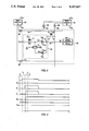
- FIG. 1 is a schematic diagram of a test structure on an integrated circuit showing intersecting probe lines and sense lines coupled to electronic switches;
- FIG. 2 is a schematic of a storage element having an output coupled to an electronic switch according to a matrix test line structure in which separate power signals are applied to the test electronics and the integrated circuit storage elements;
- FIG. 3 is a timing diagram illustrating a desired signal level forced upon the output of the storage element of FIG. 2 while power is already being applied to the integrated circuit;
- FIG. 4 is a timing diagram illustrating a desired signal level forced upon the output of the storage element of FIG. 2 at power up;
- FIG. 5 is a schematic diagram of an integrated circuit having a plurality of storage elements and a matrix of test lines
- FIG. 6 is a timing diagram illustrating the forcing of desired signal levels upon select storage elements of FIG. 5 while power is applied to the integrated circuit
- FIG. 7 is a timing diagram illustrating the forcing of desired signal levels upon select storage elements of FIG. 5 at power up.
- the integrated circuit 30 includes a storage element 40, a switch 42, a probe line 44 and a control line 46.
- the storage element 40 is a conventional storage device and is shown by way of example as a CMOS latch structure including two logic gates G1 and G2 and two transmission gates T1 and T2.
- Transmission gate T1 is for receiving a data input signal D in for defining the logic state at the storage element output line 48 during normal operation.
- the transmission gates T1 and T2 are for receiving clock and inverted clock signals which define the timing for the storage element 40.
- the signal line 48 of the storage element 40 is coupled to the switch 42 and, according to its normal operation, other logic circuitry 50.
- the switch 42 is formed of an FET transistor with the probe line 44 coupled to the gate G, the control line 46 coupled to the source S and the output line 48 coupled to the drain D.
- the logic state of the probe line 44 defines the logic state of the switch 42 (i.e., "ON"/"OFF"; "conductive/non-conductive”).
- Test contact 36 is for receiving a signal from the test electronics 32 via contact (i.e., probing) or non-contact (i.e., electro-optic) techniques to define the signal level of the probe line 44. Such signal defines the state of the switch 42.
- the control line 46 is coupled to test contact 38.
- Test contact 38 is also for receiving a signal from the test electronics 34 via contact or non-contact techniques to define the signal level of the control line 46. Such signal is applied through the switch 42 to the output line 48 of the storage element 40 while the switch 42 is in the conductive state.
- the probe line and control line signals thus are defined by the test circuits 32, 34.
- the test circuits 32, 34 include power supply lines which are independently defined relative to the power supply lines that drive the storage elements 40 and the other non-test circuitry on the integrated circuit 11. Accordingly, the power supply signal V dt for the test circuits 32, 34 may be of greater or lesser drive than that of the power supply signal V dd , or equal to the drive and voltage of that of the power supply signal V dd . Further, the test circuits 32, 34 can drive the probe lines 44, control lines 46 and switches 42 to apply a signal to the storage element even when the storage elements 40 are not receiving a power signal V dd .
- a signal is applied to the output line 48 while the drive and voltage of the power signal V dt is greater than that of the power signal V dd .
- the signal applied at the output line 48 is forced upon the storage element 40 by overpowering the signal that would otherwise occur.
- a desired signal level corresponds to a voltage level of sufficient magnitude to establish a binary logic state unambiguously, i.e., either TRUE (ON) or FALSE (OFF).
- the applied signal is provided from test electronics 34 to the test contact 38.
- Control line 46 receives the signal and carries the signal to the switch 42. With the switch 42 set to a conductive state by applying an appropriate signal along probe line 44, the desired signal is passed from the control line 46 to the output line 48.
- the greater V dt signal enables the desired signal to overpower the signal level of the output line 48.
- the desired signal overpowers the indeterminant signal level at which the output line 48 otherwise would appear at power up.
- any state-definable signal path of the element 40 may be coupled to the switch 42, instead. Accordingly, the signal output 48 of the element 40 alternatively may be invoked by applying an appropriate signal level at an input line or internal line of the element 40.
- a timing diagram is shown for setting the output line 48 to the desired signal level.
- the power signal V dt is increased to a greater drive than that of V dd , as shown by the increase in voltage (increase in current not shown).
- the probe line 44 is excited between times t 2 and t 3 turning the switch 42 on.
- a signal from the control line 46 at the desired signal level then is applied between times t 2 and t 3 to the storage element 40 (i.e., to the output line 48 at point X).
- the relative timing between the increase in drive of signal V dt , the excitation of the probe line 44 to turn on switch 42 and the application of the desired signal level to the control line 46 is not critical. Any order may be used.
- the desired signal level then can be locked in by switching the probe line signal P 1 so as to turn the switch 42 off and/or reducing the drive of the power signal V dt to be less than or equal to that of the power signal V dd .
- the power signal V dt is altered to have a drive less than or equal to that of the power signal V dd prior to normal operation or observation of the storage elements 40.
- the currents of each of the power supply signals V dt and V dd may be monitored to compare the relative drives of the two signals.
- the storage element signal 48 is not altered or disturbed by the test circuits 32, 34 during the normal operation, including the test point observation times. (Although, the timing diagram shows the desired signal level as a logic high, the desired signal level alternatively may be a logic low.)
- a timing diagram is shown for setting the output line 48 to the desired signal level at power up.
- the power to the test electronics 32 and 34 is applied at t 1 as shown by the rise in signal V dt .
- the probe line 44 is excited between times t 2 and t 3 , turning the switch 42 on.
- a signal from the control line 46 at the desired signal level then is applied between times t 2 and t 3 to the storage element 40 output line 48 at point X.
- the relative timing between the excitation of the probe line 44 to turn on switch 42 and the application of the desired signal level to the control line 46 is not critical. Either may occur first.
- corresponding probe lines 44 and control lines 46 may be accessed as described above to achieve desired signal levels at select storage elements 40a-40f.
- the integrated circuit 30 may be formed in a dense matrix structure for ease of testing as previously described in a commonly-assigned U.S. Pat. No. 4,749,947 of the same inventor issued Jun. 7, 1988 for GRID-BASED, "CROSS-CHECK” TEST STRUCTURE FOR TESTING INTEGRATED CIRCUITS, and incorporated herein by reference.
- Select storage elements 40a, 40b, 40c, 40d, 40e, 40f may be addressed by turning on a switch 42 coupled to the select storage elements as described above.
- FIG. 6 a timing diagram is shown for achieving the above desired signal level examples for the case in which the power signal V dd is already high.
- the test control circuits 32, 34 (FIG. 2) are driven harder at time t 1 relative to the drive of signal V dd , as shown by the voltage increase in line V dt .
- probe line p 1 is set high at time t 2 , while probe line p 3 is kept low.
- the first switches 42 for the storage elements 40a, 40b and 40c (FIG. 5) are activated, while the second switches 42 for storage elements 40d, 40e and 40f are inactive.
- the control lines C 1 , C 2 and C 3 are set high. This defines the outputs for Q a , Q b and Q c as desired.
- Probe line p 1 then goes low at time t 4
- probe line p 3 goes high at time t 5 to activate the second switches for storage elements 40d, 40e and 40f, while deactivating the first switches 42 for storage elements 40a, 40b and 40c.
- the control line C 1 is set high and the control line C 3 is set low.
- Q 2 is a "don't care”
- C 2 could be either low or high.
- the power signal V dt drive is restored to the previous lower level enabling the storage elements 40 to be observed without alteration or disturbance.
- FIG. 7 a timing diagram is shown for achieving the above desired signal level examples at power up.
- the output lines 48 for Q a , Q b and Q d are high and for Q c and Q f are low as desired.
- Q e which is a "don't care,” is a logic low.
- the test control circuits 32, 34 are powered up at time t 1 as shown by the rise in line V dt .
- probe line p 1 is set high at time t 2
- probe line p 3 is kept low. Accordingly, the first switches 42 for the storage elements 40a, 40b and 40c (FIG.
- the power line V dd rises at time t 6 before the charge at the respective output lines 48 dissipate. This time is defined by the interval between times t 4 and t 6 of FIG. 6.
- the use of high impedance CMOS technology for the storage elements enables the signal to be removed for a period without losing the desired signal level.
- the interval t 6 -t 4 is to be less than the discharge time for the output capacitance of each select storage element 40, typically a few milliseconds. Accordingly, the output level for a plurality of storage elements may be set to desired signal levels.
- V dd may be at a small non-zero voltage (i.e., i volt) while setting the desired signal level.
- the invention may include alternative embodiments and changes.
- a crosscheck matrix structure is described for the integrated circuit, the invention is applicable to other types of matrices and other technologies with the appropriate substitutions.
- a conventional latch has been described as the storage element structure, the invention applies to other types of storage elements and storage cells.
- test circuits 32, 34 and the probe line and sense/control line contacts 36, 38 of FIG. 2 are shown off chip, such circuits and contacts also may be included in the integrated circuit itself.
- control line signal is shown and described as imposing a logic high or logic low at a select storage element, separate control line signals may be applied through separate switches to define the respective logic high or logic low for the select storage element.
- the forcing of the storage element state is described as being accomplished by increasing the drive of the power supply signal to the test circuits 32, 34 relative to the drive of the storage element power supply signal
- the forcing can be achieved by varying the impedance of the switch so that the drive of the signal applied to the storage element has a greater drive relative to the drive of a signal appearing at the storage element output line, internal line or input line, as appropriate. Accordingly, it is the relative drives of the applied signal and the signal being overpowered which are of significance.
- the relative power signals altered are described as V dt and V dd , the relative power signals may be the corresponding ground signals, V st and V ss .
Abstract
Description
Claims (24)
Priority Applications (2)
| Application Number | Priority Date | Filing Date | Title |
|---|---|---|---|
| US07/554,313 US5157627A (en) | 1990-07-17 | 1990-07-17 | Method and apparatus for setting desired signal level on storage element |
| KR1019910000008A KR920003307A (en) | 1990-07-17 | 1991-01-03 | Apparatus and method for setting desired signal level on storage element |
Applications Claiming Priority (1)
| Application Number | Priority Date | Filing Date | Title |
|---|---|---|---|
| US07/554,313 US5157627A (en) | 1990-07-17 | 1990-07-17 | Method and apparatus for setting desired signal level on storage element |
Publications (1)
| Publication Number | Publication Date |
|---|---|
| US5157627A true US5157627A (en) | 1992-10-20 |
Family
ID=24212887
Family Applications (1)
| Application Number | Title | Priority Date | Filing Date |
|---|---|---|---|
| US07/554,313 Expired - Fee Related US5157627A (en) | 1990-07-17 | 1990-07-17 | Method and apparatus for setting desired signal level on storage element |
Country Status (2)
| Country | Link |
|---|---|
| US (1) | US5157627A (en) |
| KR (1) | KR920003307A (en) |
Cited By (11)
| Publication number | Priority date | Publication date | Assignee | Title |
|---|---|---|---|---|
| US5291448A (en) * | 1990-06-21 | 1994-03-01 | Sgs-Thomson Microelectronics, S.A. | Zone-segregated circuit for the testing of electrically programmable memory cells |
| US5619157A (en) * | 1993-12-14 | 1997-04-08 | Sony Corporation | Synchronizing circuit with dynamic and static latch circuitry |
| US5657328A (en) * | 1993-11-19 | 1997-08-12 | Texas Instruments Incorporated | Scan design with expanded access capability |
| EP0805459A1 (en) * | 1996-04-30 | 1997-11-05 | Texas Instruments Incorporated | Method and apparatus for testing DRAM memory units |
| US5936876A (en) * | 1997-12-03 | 1999-08-10 | Lsi Logic Corporation | Semiconductor integrated circuit core probing for failure analysis |
| US6331790B1 (en) | 2000-03-10 | 2001-12-18 | Easic Corporation | Customizable and programmable cell array |
| US6584592B2 (en) * | 1998-06-16 | 2003-06-24 | Mitsubishi Denki Kabushiki Kaisha | Semiconductor testing apparatus for testing semiconductor device including built in self test circuit |
| US6756811B2 (en) | 2000-03-10 | 2004-06-29 | Easic Corporation | Customizable and programmable cell array |
| US6933747B1 (en) * | 2003-10-10 | 2005-08-23 | Xilinx, Inc. | Structures and methods of testing interconnect structures in programmable logic devices |
| US20060023540A1 (en) * | 2004-07-28 | 2006-02-02 | Kabushiki Kaisha Toshiba | Semiconductor storage device |
| US7023233B1 (en) * | 2004-10-12 | 2006-04-04 | Advantest Corporation | Test apparatus and test method |
Citations (9)
| Publication number | Priority date | Publication date | Assignee | Title |
|---|---|---|---|---|
| US3761675A (en) * | 1972-01-19 | 1973-09-25 | Hughes Aircraft Co | Material cutting and printing system |
| US3795859A (en) * | 1972-07-03 | 1974-03-05 | Ibm | Method and apparatus for determining the electrical characteristics of a memory cell having field effect transistors |
| US3806891A (en) * | 1972-12-26 | 1974-04-23 | Ibm | Logic circuit for scan-in/scan-out |
| US4293919A (en) * | 1979-08-13 | 1981-10-06 | International Business Machines Corporation | Level sensitive scan design (LSSD) system |
| US4513418A (en) * | 1982-11-08 | 1985-04-23 | International Business Machines Corporation | Simultaneous self-testing system |
| US4517672A (en) * | 1981-09-07 | 1985-05-14 | Siemens Aktiengesellschaft | Method and arrangement for an operational check of a programmable logic array |
| US4613970A (en) * | 1983-02-04 | 1986-09-23 | Hitachi, Ltd. | Integrated circuit device and method of diagnosing the same |
| EP0223714A2 (en) * | 1985-11-20 | 1987-05-27 | Fujitsu Limited | Semiconductor integrated circuit device with test circuit |
| US4749947A (en) * | 1986-03-10 | 1988-06-07 | Cross-Check Systems, Inc. | Grid-based, "cross-check" test structure for testing integrated circuits |
-
1990
- 1990-07-17 US US07/554,313 patent/US5157627A/en not_active Expired - Fee Related
-
1991
- 1991-01-03 KR KR1019910000008A patent/KR920003307A/en not_active Application Discontinuation
Patent Citations (9)
| Publication number | Priority date | Publication date | Assignee | Title |
|---|---|---|---|---|
| US3761675A (en) * | 1972-01-19 | 1973-09-25 | Hughes Aircraft Co | Material cutting and printing system |
| US3795859A (en) * | 1972-07-03 | 1974-03-05 | Ibm | Method and apparatus for determining the electrical characteristics of a memory cell having field effect transistors |
| US3806891A (en) * | 1972-12-26 | 1974-04-23 | Ibm | Logic circuit for scan-in/scan-out |
| US4293919A (en) * | 1979-08-13 | 1981-10-06 | International Business Machines Corporation | Level sensitive scan design (LSSD) system |
| US4517672A (en) * | 1981-09-07 | 1985-05-14 | Siemens Aktiengesellschaft | Method and arrangement for an operational check of a programmable logic array |
| US4513418A (en) * | 1982-11-08 | 1985-04-23 | International Business Machines Corporation | Simultaneous self-testing system |
| US4613970A (en) * | 1983-02-04 | 1986-09-23 | Hitachi, Ltd. | Integrated circuit device and method of diagnosing the same |
| EP0223714A2 (en) * | 1985-11-20 | 1987-05-27 | Fujitsu Limited | Semiconductor integrated circuit device with test circuit |
| US4749947A (en) * | 1986-03-10 | 1988-06-07 | Cross-Check Systems, Inc. | Grid-based, "cross-check" test structure for testing integrated circuits |
Non-Patent Citations (10)
| Title |
|---|
| "A Logic Design Structure for LSI Testability", Eichelberger, et al., Proceedings -th Design Automation Conf., Jun., 1977. |
| "Built-in Self-Test Structures" by E. J. McClusky, IEEE Design and Test, vol. 2, No. 2, pp. 29-36. |
| "Built-in Self-Test Techniques" by E. J. McClusky, IEEE Design and Test, vol. 2, No. 2, pp. 21-28. |
| "Design for Testability -A Survey", by T. W. Williams, et al., Proceedings IEEE, vol. 71, pp. 359-416, Jan. 1983. |
| "Voltage Checking Device" by G. Canard and A. Potocki, IBM Technical Disclosure Bulletin, vol. 8, No. 5, Oct. 1965. |
| A Logic Design Structure for LSI Testability , Eichelberger, et al., Proceedings th Design Automation Conf., Jun., 1977. * |
| Built in Self Test Structures by E. J. McClusky, IEEE Design and Test, vol. 2, No. 2, pp. 29 36. * |
| Built in Self Test Techniques by E. J. McClusky, IEEE Design and Test, vol. 2, No. 2, pp. 21 28. * |
| Design for Testability A Survey , by T. W. Williams, et al., Proceedings IEEE, vol. 71, pp. 359 416, Jan. 1983. * |
| Voltage Checking Device by G. Canard and A. Potocki, IBM Technical Disclosure Bulletin, vol. 8, No. 5, Oct. 1965. * |
Cited By (26)
| Publication number | Priority date | Publication date | Assignee | Title |
|---|---|---|---|---|
| US5291448A (en) * | 1990-06-21 | 1994-03-01 | Sgs-Thomson Microelectronics, S.A. | Zone-segregated circuit for the testing of electrically programmable memory cells |
| US5657328A (en) * | 1993-11-19 | 1997-08-12 | Texas Instruments Incorporated | Scan design with expanded access capability |
| US5619157A (en) * | 1993-12-14 | 1997-04-08 | Sony Corporation | Synchronizing circuit with dynamic and static latch circuitry |
| CN1049539C (en) * | 1993-12-14 | 2000-02-16 | 索尼公司 | Synchronizing circuit |
| EP0805459A1 (en) * | 1996-04-30 | 1997-11-05 | Texas Instruments Incorporated | Method and apparatus for testing DRAM memory units |
| US5936876A (en) * | 1997-12-03 | 1999-08-10 | Lsi Logic Corporation | Semiconductor integrated circuit core probing for failure analysis |
| US6584592B2 (en) * | 1998-06-16 | 2003-06-24 | Mitsubishi Denki Kabushiki Kaisha | Semiconductor testing apparatus for testing semiconductor device including built in self test circuit |
| US20050024086A1 (en) * | 2000-03-10 | 2005-02-03 | Easic Corporation | Customizable and programmable cell array |
| US6989687B2 (en) | 2000-03-10 | 2006-01-24 | Easic Corporation | Customizable and programmable cell array |
| US6756811B2 (en) | 2000-03-10 | 2004-06-29 | Easic Corporation | Customizable and programmable cell array |
| US6819136B2 (en) | 2000-03-10 | 2004-11-16 | Easic Corporation | Customizable and programmable cell array |
| US20050015699A1 (en) * | 2000-03-10 | 2005-01-20 | Easic Corporation | Customizable and programmable cell array |
| US6331790B1 (en) | 2000-03-10 | 2001-12-18 | Easic Corporation | Customizable and programmable cell array |
| US6930511B2 (en) | 2000-03-10 | 2005-08-16 | Easic Corporation | Array of programmable cells with customized interconnections |
| US20060176075A1 (en) * | 2000-03-10 | 2006-08-10 | Easic Corporation | Customizable and Programmable Cell Array |
| US6985012B2 (en) | 2000-03-10 | 2006-01-10 | Easic Corporation | Customizable and programmable cell array |
| US6642744B2 (en) | 2000-03-10 | 2003-11-04 | Easic Corporation | Customizable and programmable cell array |
| US7068070B2 (en) | 2000-03-10 | 2006-06-27 | Easic Corporation | Customizable and programmable cell array |
| US20060028242A1 (en) * | 2000-03-10 | 2006-02-09 | Easic Corporation | Customizable and programmable cell array |
| US6933747B1 (en) * | 2003-10-10 | 2005-08-23 | Xilinx, Inc. | Structures and methods of testing interconnect structures in programmable logic devices |
| US20060023540A1 (en) * | 2004-07-28 | 2006-02-02 | Kabushiki Kaisha Toshiba | Semiconductor storage device |
| US7095652B2 (en) * | 2004-07-28 | 2006-08-22 | Kabushiki Kaisha Toshiba | Semiconductor storage device |
| US7023233B1 (en) * | 2004-10-12 | 2006-04-04 | Advantest Corporation | Test apparatus and test method |
| US20060076973A1 (en) * | 2004-10-12 | 2006-04-13 | Advantest Corporation | Test apparatus and test method |
| US20060114015A1 (en) * | 2004-10-12 | 2006-06-01 | Advantest Corporation | Test apparatus and test method |
| US7298162B2 (en) * | 2004-10-12 | 2007-11-20 | Advantest Corporation | Test apparatus and test method |
Also Published As
| Publication number | Publication date |
|---|---|
| KR920003307A (en) | 1992-02-29 |
Similar Documents
| Publication | Publication Date | Title |
|---|---|---|
| US9829538B2 (en) | IC expected data and mask data on I/O data pads | |
| US4821238A (en) | Semiconductor memory device having test pattern generating circuit | |
| US20170146597A1 (en) | Reduced signaling interface method & apparatus | |
| US5157627A (en) | Method and apparatus for setting desired signal level on storage element | |
| EP0954866B1 (en) | Sdram clocking test mode | |
| EP0336444B1 (en) | Semiconductor integrated circuit device having improved input/output interface circuit | |
| JPH1139898A (en) | Semiconductor device | |
| US6865705B2 (en) | Semiconductor integrated circuit device capable of switching mode for trimming internal circuitry through JTAG boundary scan method | |
| US5202624A (en) | Interface between ic operational circuitry for coupling test signal from internal test matrix | |
| US6133053A (en) | Circuit and a method for configuring pad connections in an integrated device | |
| US5179534A (en) | Method and apparatus for setting desired logic state at internal point of a select storage element | |
| US5230001A (en) | Method for testing a sequential circuit by splicing test vectors into sequential test pattern | |
| EP0213453B1 (en) | Noise reduction during testing of integrated circuit chips | |
| US5206862A (en) | Method and apparatus for locally deriving test signals from previous response signals | |
| US4868413A (en) | Testable passgate logic circuits | |
| US4894800A (en) | Reconfigurable register bit-slice for self-test | |
| US20020078400A1 (en) | Self-test with split, asymmetric controlled driver output stage | |
| KR20020087103A (en) | Method and apparatus for an easy identification of a state of a dram generator controller | |
| KR100465541B1 (en) | Semiconductor test device with mulit probing pad | |
| KR0147453B1 (en) | Semiconductor integrated circuit | |
| KR19990039586A (en) | How to test memory devices with reduced number of test pads | |
| JPS59200456A (en) | Semiconductor integrated circuit device | |
| KR100487497B1 (en) | Device and method for controling internal signal of semiconductor memory device | |
| KR19990039587A (en) | Memory device test method with reduced number of test pins | |
| JPH03127846A (en) | Integrated circuit device |
Legal Events
| Date | Code | Title | Description |
|---|---|---|---|
| AS | Assignment |
Owner name: CROSS-CHECK SYSTEMS, INC., A CORP OF DE, CALIFORNI Free format text: ASSIGNMENT OF ASSIGNORS INTEREST.;ASSIGNOR:GHEEWALA, TUSHAR;REEL/FRAME:005380/0692 Effective date: 19900717 |
|
| AS | Assignment |
Owner name: CROSSCHECK TECHNOLOGY, INC., CALIFORNIA Free format text: ASSIGNMENT OF ASSIGNORS INTEREST.;ASSIGNOR:CROSS-CHECK SYSTEMS, INC., A DE CORP.;REEL/FRAME:006196/0250 Effective date: 19920714 |
|
| FEPP | Fee payment procedure |
Free format text: PAT HLDR NO LONGER CLAIMS SMALL ENT STAT AS INDIV INVENTOR (ORIGINAL EVENT CODE: LSM1); ENTITY STATUS OF PATENT OWNER: LARGE ENTITY |
|
| FEPP | Fee payment procedure |
Free format text: PAYOR NUMBER ASSIGNED (ORIGINAL EVENT CODE: ASPN); ENTITY STATUS OF PATENT OWNER: LARGE ENTITY |
|
| FPAY | Fee payment |
Year of fee payment: 4 |
|
| AS | Assignment |
Owner name: DUET TECHNOLOGIES, INC., CALIFORNIA Free format text: ASSIGNMENT OF ASSIGNORS INTEREST;ASSIGNOR:CROSSCHECK TECHNOLOGY, INC.;REEL/FRAME:008568/0375 Effective date: 19970116 |
|
| REMI | Maintenance fee reminder mailed | ||
| LAPS | Lapse for failure to pay maintenance fees | ||
| FP | Lapsed due to failure to pay maintenance fee |
Effective date: 20001020 |
|
| STCH | Information on status: patent discontinuation |
Free format text: PATENT EXPIRED DUE TO NONPAYMENT OF MAINTENANCE FEES UNDER 37 CFR 1.362 |