US5155820A - Instruction format with designations for operand lengths of byte, half word, word, or double word encoded in address bits - Google Patents
Instruction format with designations for operand lengths of byte, half word, word, or double word encoded in address bits Download PDFInfo
- Publication number
- US5155820A US5155820A US07/313,704 US31370489A US5155820A US 5155820 A US5155820 A US 5155820A US 31370489 A US31370489 A US 31370489A US 5155820 A US5155820 A US 5155820A
- Authority
- US
- United States
- Prior art keywords
- instruction
- operand
- data
- processor
- word
- Prior art date
- Legal status (The legal status is an assumption and is not a legal conclusion. Google has not performed a legal analysis and makes no representation as to the accuracy of the status listed.)
- Expired - Fee Related
Links
- 238000012545 processing Methods 0.000 claims description 50
- 238000012360 testing method Methods 0.000 claims description 4
- 230000015654 memory Effects 0.000 abstract description 175
- 238000000034 method Methods 0.000 abstract description 47
- 230000008569 process Effects 0.000 abstract description 47
- 239000000872 buffer Substances 0.000 abstract description 37
- 238000005192 partition Methods 0.000 abstract description 34
- 238000012546 transfer Methods 0.000 abstract description 18
- 230000000694 effects Effects 0.000 abstract description 5
- 238000007667 floating Methods 0.000 description 36
- 230000006870 function Effects 0.000 description 17
- 238000007792 addition Methods 0.000 description 13
- 230000000295 complement effect Effects 0.000 description 13
- 239000013598 vector Substances 0.000 description 12
- 238000013461 design Methods 0.000 description 11
- 230000005540 biological transmission Effects 0.000 description 5
- 238000004891 communication Methods 0.000 description 5
- 238000011156 evaluation Methods 0.000 description 4
- 208000018634 fetal akinesia deformation sequence Diseases 0.000 description 4
- 208000012165 fetal akinesia deformation sequence syndrome Diseases 0.000 description 4
- 238000002421 fluorescence-activated droplet sorting Methods 0.000 description 4
- 238000005516 engineering process Methods 0.000 description 3
- 238000011112 process operation Methods 0.000 description 3
- 102100032489 Heat shock 70 kDa protein 13 Human genes 0.000 description 2
- 101001016638 Homo sapiens Heat shock 70 kDa protein 13 Proteins 0.000 description 2
- 208000026940 Microvillus inclusion disease Diseases 0.000 description 2
- 101000720079 Stichodactyla helianthus DELTA-stichotoxin-She4a Proteins 0.000 description 2
- FFBHFFJDDLITSX-UHFFFAOYSA-N benzyl N-[2-hydroxy-4-(3-oxomorpholin-4-yl)phenyl]carbamate Chemical compound OC1=C(NC(=O)OCC2=CC=CC=C2)C=CC(=C1)N1CCOCC1=O FFBHFFJDDLITSX-UHFFFAOYSA-N 0.000 description 2
- 238000004364 calculation method Methods 0.000 description 2
- 238000006243 chemical reaction Methods 0.000 description 2
- 230000007246 mechanism Effects 0.000 description 2
- 230000001360 synchronised effect Effects 0.000 description 2
- 230000007704 transition Effects 0.000 description 2
- UYBGHBAVRNATET-VQTJNVASSA-N 1,3-dimethoxy-2-[(1r,6r)-3-methyl-6-prop-1-en-2-ylcyclohex-2-en-1-yl]-5-pentylbenzene Chemical compound COC1=CC(CCCCC)=CC(OC)=C1[C@H]1[C@H](C(C)=C)CCC(C)=C1 UYBGHBAVRNATET-VQTJNVASSA-N 0.000 description 1
- JBRZTFJDHDCESZ-UHFFFAOYSA-N AsGa Chemical compound [As]#[Ga] JBRZTFJDHDCESZ-UHFFFAOYSA-N 0.000 description 1
- NOQGZXFMHARMLW-UHFFFAOYSA-N Daminozide Chemical compound CN(C)NC(=O)CCC(O)=O NOQGZXFMHARMLW-UHFFFAOYSA-N 0.000 description 1
- 102100032170 GTP-binding protein SAR1b Human genes 0.000 description 1
- 229910001218 Gallium arsenide Inorganic materials 0.000 description 1
- 101001130192 Homo sapiens Lipid droplet-associated hydrolase Proteins 0.000 description 1
- 101100041709 Homo sapiens SAR1B gene Proteins 0.000 description 1
- 102100031360 Lipid droplet-associated hydrolase Human genes 0.000 description 1
- 101100496108 Mus musculus Clec2h gene Proteins 0.000 description 1
- 208000003019 Neurofibromatosis 1 Diseases 0.000 description 1
- 101710111444 Nitric oxide synthase, brain Proteins 0.000 description 1
- 101710123927 Probable succinate-semialdehyde dehydrogenase [NADP(+)] Proteins 0.000 description 1
- 101710143049 Succinate-semialdehyde dehydrogenase [NADP(+)] Proteins 0.000 description 1
- 102100023673 Succinate-semialdehyde dehydrogenase, mitochondrial Human genes 0.000 description 1
- 108010039203 Tripeptidyl-Peptidase 1 Proteins 0.000 description 1
- 102100034197 Tripeptidyl-peptidase 1 Human genes 0.000 description 1
- 230000009471 action Effects 0.000 description 1
- 230000017488 activation-induced cell death of T cell Effects 0.000 description 1
- 238000003491 array Methods 0.000 description 1
- 230000003139 buffering effect Effects 0.000 description 1
- 230000008859 change Effects 0.000 description 1
- 238000012885 constant function Methods 0.000 description 1
- 238000013500 data storage Methods 0.000 description 1
- 238000010586 diagram Methods 0.000 description 1
- 238000006073 displacement reaction Methods 0.000 description 1
- 230000009977 dual effect Effects 0.000 description 1
- 208000014402 familial multiple discoid fibromas Diseases 0.000 description 1
- 230000014759 maintenance of location Effects 0.000 description 1
- 230000008520 organization Effects 0.000 description 1
- 230000011664 signaling Effects 0.000 description 1
- 239000000725 suspension Substances 0.000 description 1
- 238000010200 validation analysis Methods 0.000 description 1
Images


Classifications
-
- G—PHYSICS
- G06—COMPUTING; CALCULATING OR COUNTING
- G06F—ELECTRIC DIGITAL DATA PROCESSING
- G06F9/00—Arrangements for program control, e.g. control units
- G06F9/06—Arrangements for program control, e.g. control units using stored programs, i.e. using an internal store of processing equipment to receive or retain programs
- G06F9/30—Arrangements for executing machine instructions, e.g. instruction decode
- G06F9/30003—Arrangements for executing specific machine instructions
- G06F9/30007—Arrangements for executing specific machine instructions to perform operations on data operands
- G06F9/3001—Arithmetic instructions
- G06F9/30014—Arithmetic instructions with variable precision
-
- G—PHYSICS
- G06—COMPUTING; CALCULATING OR COUNTING
- G06F—ELECTRIC DIGITAL DATA PROCESSING
- G06F9/00—Arrangements for program control, e.g. control units
- G06F9/06—Arrangements for program control, e.g. control units using stored programs, i.e. using an internal store of processing equipment to receive or retain programs
- G06F9/30—Arrangements for executing machine instructions, e.g. instruction decode
- G06F9/30003—Arrangements for executing specific machine instructions
- G06F9/30007—Arrangements for executing specific machine instructions to perform operations on data operands
- G06F9/30021—Compare instructions, e.g. Greater-Than, Equal-To, MINMAX
-
- G—PHYSICS
- G06—COMPUTING; CALCULATING OR COUNTING
- G06F—ELECTRIC DIGITAL DATA PROCESSING
- G06F9/00—Arrangements for program control, e.g. control units
- G06F9/06—Arrangements for program control, e.g. control units using stored programs, i.e. using an internal store of processing equipment to receive or retain programs
- G06F9/30—Arrangements for executing machine instructions, e.g. instruction decode
- G06F9/30145—Instruction analysis, e.g. decoding, instruction word fields
- G06F9/3016—Decoding the operand specifier, e.g. specifier format
- G06F9/30167—Decoding the operand specifier, e.g. specifier format of immediate specifier, e.g. constants
-
- G—PHYSICS
- G06—COMPUTING; CALCULATING OR COUNTING
- G06F—ELECTRIC DIGITAL DATA PROCESSING
- G06F9/00—Arrangements for program control, e.g. control units
- G06F9/06—Arrangements for program control, e.g. control units using stored programs, i.e. using an internal store of processing equipment to receive or retain programs
- G06F9/30—Arrangements for executing machine instructions, e.g. instruction decode
- G06F9/38—Concurrent instruction execution, e.g. pipeline, look ahead
- G06F9/3824—Operand accessing
-
- G—PHYSICS
- G06—COMPUTING; CALCULATING OR COUNTING
- G06F—ELECTRIC DIGITAL DATA PROCESSING
- G06F9/00—Arrangements for program control, e.g. control units
- G06F9/06—Arrangements for program control, e.g. control units using stored programs, i.e. using an internal store of processing equipment to receive or retain programs
- G06F9/30—Arrangements for executing machine instructions, e.g. instruction decode
- G06F9/38—Concurrent instruction execution, e.g. pipeline, look ahead
- G06F9/3836—Instruction issuing, e.g. dynamic instruction scheduling or out of order instruction execution
- G06F9/3838—Dependency mechanisms, e.g. register scoreboarding
-
- G—PHYSICS
- G06—COMPUTING; CALCULATING OR COUNTING
- G06F—ELECTRIC DIGITAL DATA PROCESSING
- G06F9/00—Arrangements for program control, e.g. control units
- G06F9/06—Arrangements for program control, e.g. control units using stored programs, i.e. using an internal store of processing equipment to receive or retain programs
- G06F9/30—Arrangements for executing machine instructions, e.g. instruction decode
- G06F9/38—Concurrent instruction execution, e.g. pipeline, look ahead
- G06F9/3885—Concurrent instruction execution, e.g. pipeline, look ahead using a plurality of independent parallel functional units
Definitions
- the invention disclosed broadly relates to data processing systems and more particularly relates to processing elements within a data processing system. Even more particularly, the invention relates to the instruction execution mechanisms of such processors and the data handling associated with these mechanisms.
- Present day computers are machines that accept instructions and data and produce results from the data according to their instructions. They are made up of elements that communicate with the external world, store data, change the forms of the data, and convert their instructions (which are moved around within the computer as data) into the signals that control the computer's activity.
- This invention is concerned with those components of the computer, called processing units or elements, that actually carry out the computations.
- a processing element is typically constructed of one or more circuits that convert the instructions into control signals and perform certain computations, one or more memory circuits for temporarily storing the data to be operated on and the results, and the communications links, or buses, capable of communicating data, instructions, and results between the processing and memory circuits.
- the present invention consists of an arrangement for connecting the various processing and memory circuits together and a set of instructions for the resulting processor.
- the most important attributes to be considered are its processing speed, its versatility, and its overall cost.
- the present invention is designed so that it is partitioned in such a way that very fast technologies can be used to implement its critical parts and the overall processing element can be customized according to the application.
- speed was the primary design criterion used in formulating this invention, it achieves a good speed to cost ratio by using relatively simple circuits and connections between these circuits. It is the simplicity of the circuits that allows them to be implemented using low-density, but very fast technologies such as those based on gallium arsenide.
- the architecture contains only two primary internal buses so that, even though the processing element may include several integrated circuits, the power dissipation is kept at a reasonable level. Each integrated circuit would be required to drive only one of these buses and the width and speed of these buses could be set according to the design requirements.
- the invention is comprised of a control unit and a very high speed register set/data RAM combination which constitutes its central memory.
- the control unit receives its instructions from a code stream and uses the instructions to transfer data from the central memory to a parallel set of processing circuits over an output bus.
- the processing circuits also receive from the control unit that portion of the instructions that indicates which processing circuit is to perform the computation and the precise form of the computation.
- the selected processing circuit acts as a simple transponder that inputs the data, performs its computation and returns its result(s) to the central memory via an input bus.
- the instruction execution is coordinated with the arrival of results using a destination validation scheme similar to the scheme often referred to as scoreboarding (see Richard Y. Kain, Computer Architecture: Hardware and Software, Vol.
- Scoreboarding attaches a valid bit to each data location in the local store of the processor.
- the present invention retains the destination addresses of data in the local store of the control unit until the corresponding results are returned by the processing circuits.
- the present invention does use valid bits on the destination addresses to denote when the destination address is being used by a processing circuit, but it does not have a valid bit associated with each local store address.
- the present invention allows for the automatic inputting and outputting of sequential data to and from its central memory. This is done by using partitions and, perhaps, first-in/first-out (FIFO) buffers within the central memory.
- FIFO first-in/first-out
- the overall architecture of the present invention is similar to that of the invention described in Trubisky et al, U.S. Pat. No. 4,521,851, issued Jun. 4, 1985 (the '851 patent), but it also differs from the '851 patent in several respects.
- the '851 patent also uses separate code and data streams, a central memory, multiple processors, and an output bus for sending source operands to the processors and an input bus for returning results.
- the '851 patent uses a conventional data cache for its central memory, includes separate first-in/first-out buffers for temporarily storing the results until they can be returned to the data cache, coordinates the return of the results with the instruction's execution by including a second instruction execution queue that is associated with the result storage circuitry, and does not provide for automatic prefetching and storing of array data.
- the processors in the '851 patent serve specific purposes, some of which are related to address calculations. Address calculations are not applicable to the present architecture because it uses only the immediate, direct, and register indirect addressing modes. The equivalent of base, index, and virtual addressing is left to external circuitry such as that described in the invention given in patent application (B) of the foregoing list of copending patent applications.
- the processors indicated in the present invention may serve extremely varied purposes and may be designed to fit a specific application. Communication with the external data memory hierarchy is handled by one of the processors, the I/O processor, instead of a data cache as in the '851 patent. A final observation is that the architecture of the '851 patent must be synchronous. For the invention herein disclosed, because of the simplicity of the control unit/central memory design and the subdivision separating this circuitry from the processors, it is possible to use either a synchronous or an asynchronous design for of the components--the control unit, the central memory, or any or all of the processors. The use of asynchronous circuitry is highly desirable when designing very high speed circuitry.
- Another object of this invention is to allow the use of the low order address bits of the operands in the instructions to define the length of the operands.
- a further object of the present invention is to allow the use of bits within each instruction of a particular type to select one of a plurality of sub processing elements which is capable of executing the instruction.
- Still another object is to provide instruction processors capable of performing sum of squares operations, sum of products operations, product of sums operations, and a series of consecutive products operations without returning a result to the central memory.
- the present invention defines an architecture that consists of a control unit, a central memory, a set of parallel processing circuits, called processors, and an output bus and an input bus for providing the necessary communication.
- the control unit receives the instructions and partially decodes them so that it can direct the outputting of the source operands from and inputting of the results to the central memory.
- a portion of each instruction is passed on to the processors and is used to select the processor to be used and specify precisely what computation is to be performed.
- a processor Upon receiving an instruction, a processor inputs the data that is sent to it over the output bus from the central memory and outputs its result(s) to the input bus which conveys the result(s) to the central memory.
- One of the processors, the I/O processor is charged with handling all communications with the external data memory hierarchy.
- the control unit includes the circuitry for arbitrating the usage of the input bus and retaining the central memory destination addresses until the corresponding results are returned from the processors. Instruction execution can continue and can be overlapped until:
- a source operand address is encountered that is the same as that of a pending result or input datum.
- the execution of the present instruction is suspended until the state causing the suspension is cleared (i.e., the needed processor becomes ready to accept operands, the needed result or input datum is put in its destination, or the required previous instructions have been completed).
- the first case is enforced by ready signals from the processors to the control unit, the second case by comparing source operand addresses to the destination addresses of the instructions currently being executed, and the third case by forcing instructions involving conditional branches to wait until the condition flags have been set by the previous instructions.
- the length of the operands of each instruction is determined partially by the low order address bits of the operand address. If the operand does not address a byte operand, the low order bit is not needed to address any datum larger than a byte, so this bit is used to determine if the operand addresses a half-word. If the operand does not address a half-word, the next low order address bit determines if it addresses a word or doubleword.
- Some of the instruction processors have multiple sub instruction processors within them, and bits in the instruction select which of the multiple sub instruction processors will be used to execute each particular instruction.
- FIG. 1 shows the overall architecture of the processing element described in the present invention.
- FIG. 2 gives an example of using circular partitions to add long vectors.
- FIG. 3 shows the detailed control unit/central memory connections and the output bus, input bus, and instruction/status bus definitions.
- FIG. 4 shows the overall architecture with the specific set of processors defined by the present invention.
- FIG. 5 shows the format of a destination address register.
- FIG. 6 shows the major components of the compare processor.
- FIG. 7 shows the major components of the logical processor.
- FIG. 8 shows the major components of the floating point processor.
- FIG. 9 shows the major components of the shift/rotate processor.
- FIG. 10 shows the major components of the add/subtract processor.
- FIG. 11 shows the major components of the multiply/divide processor.
- FIG. 12 shows the major components of the negate/complement/move processor.
- FIG. 13 shows the major components of the I/O processor.
- FIG. 14 shows the format of the I/O processor's status register.
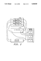
- FIG. 1 the overall architecture related to the present invention, the Processing Element 19, is illustrated.
- This architecture is such that the instructions are input to and the status is output from the Processing Element 19 over the Instruction/status Bus 27, and the data is input to and output from the Processing Element 19 over the Processor Bus (PB) 14.
- PB Processor Bus
- the major components o the Processing Element 19 are the Control Unit 30 that controls the activity within the Processing Element 19, the Central Memory 70 that provides for temporary data storage, the Input/output (I/O) Processor 200 that handles all I/O between the Processing Element 19 and the external data memory hierarchy, a set of other processors that perform the computations, an Output Bus 120 that transfers source operands from the Central Memory 70 to the I/O Processor 200 and other processors, and the Input Bus 130 that transfers input from the I/O Processor 200 and results from the other processors to the Central Memory 70.
- I/O Input/output
- the Central Memory 70 is primarily a buffer that is used by the Control Unit 30 as it directs the flow of data from and to the I/O Processor 200 and other processors according to the instructions it receives from the code stream. Data is brought into the Processing Element 19 by the I/O Processor 200 via the PB 14 and transferred to the Central Memory 70 via the Input Bus 130. Once the data is in the Central Memory 70 the instructions arriving at the Control Unit 30 via the Instruction/status Bus 27 may cause the data to be directed to the various other processors over the Output Bus 10 and be used as source operands by the other processors. The results may then be directed, according to the instructions, to be returned to the Central Memory 70 over the Input Bus 130. These results may be used by succeeding instructions as source operands in further computations.
- the contents of the Central Memory 70 may be cycled through the other processors and back into the Central Memory 70 as many times as required to complete a needed computation.
- an instruction may direct data in the Central Memory 70 to be transferred to the I/O Processor 200 which would then output the data to external memory via PB 14.
- the inputting, circulating, and outputting are under direction of the Control Unit 30 and the Central Memory 70 provides the buffering.
- the instructions entering the Control Unit 30 may be inline or may come from subprogram instruction sequences. However, if subprograms are used there must be some means of storing and retrieving return addresses. This could be done by using either a last-in/first-out (LIFO) stack that is internal to the Processing Element 19 or a LIFO stack that is maintained in the external data memory.
- LIFO last-in/first-out
- the preferred embodiment assumes that the instruction sequence is inline when it arrives at the Control Unit 30, but other designs that include the concepts of this invention may be derived that have the Control Unit 30 execute subprogram calls and returns.
- the preferred embodiment also assumes that the code and data streams are separate. However, the Instruction/status Bus 27 and the PB 14 could be combined into a single bus which is used to transfer both code and data.
- Instruction execution may proceed until a needed processor cannot accept its source operands, needed source operands are to be taken from Central Memory 70 locations that are awaiting results, or, for conditional branch instructions, the flags needed to make the decision have not yet been set according to previous instructions. If a location in the Central Memory 70 is the destination of a result or input datum but the result or input datum has not yet been put into the location, then the location is said to be invalid. Otherwise, the location is said to be valid.
- the indication (directly or indirectly) of the address of a destination operand by an instruction causes the corresponding location to become invalid and the arrival of a result or input datum at an invalid location causes it to become valid. Also, a location that is to be output from next by the automated input/output facility (discussed below) becomes invalid when output from the automated facility becomes blocked and becomes valid when this output becomes unblocked.
- the execution of an instruction may proceed by having the Control Unit 30:
- step (1) Indicate to the processors that an instruction has been output and note whether or not there is a first source operand. If there is, execution proceeds with step (2); otherwise execution proceeds with step (9).
- step (3) Note whether or not the first source operand is not immediate (i.e., not contained in the instruction). If it is not immediate, execution proceeds with step (3); otherwise execution proceeds with step (4).
- step (6) Note whether or not there is a second source operand. If there is, execution proceeds with step (6); otherwise execution proceeds with step (9).
- step (6) Note whether or not the second operand is not immediate. If it is not immediate, execution proceeds with step (7); otherwise execution proceeds with step (8).
- FIG. 1 also includes a subset of locations in the Central Memory 70 that is referred to as a Circular partition (CP) 75 and is used to provide automated input to and output from the Central Memory 70.
- CP Circular partition
- the concept of circular partitions is detailed in patent application (D) of the foregoing list of copending patent applications.
- the locations in the CP 75 have consecutive addresses and are treated as a circular memory with the location having the lowest address being considered to be adjacent to and following the location with the highest address.
- the circular partition has associated with it a pair of address pointer locations, called its rotating pair, which contain addresses of locations within the circular partition.
- the rotating pair may be implemented as locations in the Central Memory 70 or may be separate registers.
- the logic surrounding the rotating pair that is used to control the inputting to and outputting from the CP 75 is called the rotating pair logic (RPL).
- RPL rotating pair logic
- the contents of the location in the rotating pair used to input the next datum into the CP 75 is called the input pointer and the contents of the other location in the rotating pair is used to output the next datum from the CP 75 and is called the output pointer.
- Each of the pointers in the rotating pair is such that it autoincrements after each time it is used to supply an address in the CP 75.
- This autoincrementing is done such that if the addresses in the CP 75 are N through N+p-1, N+i is the address currently contained in the pointer, and n>0 is the increment amount, then the next value of the pointer is N+(i+n) modulo p.
- a pointer in the rotating pair is said to be unblocked if it can be used to address a location in the CP 75; otherwise it is blocked. Because a pointer only increments after it is used for addressing, it must be unblocked before it can be incremented. Conversely, if a pointer is unblocked it can be incremented because it can be used for addressing.
- the input and output pointers in the rotating pair must obey the following rules:
- the input pointer must initially be in its unblocked state and the output pointer must initially be in its blocked state if it is equal to the input pointer.
- the CP 75 is initialized by setting its base (lowest) address and length (although these values may be permanently set by the design) and by setting the initial addresses and increment amounts of the pointers in the rotating pair. Normally the pointers are both initially set to the base address and their increment amounts are set to be the same.
- the Central Memory 70 may include several such partitions and their associated rotating pairs and other logic.
- the purpose of a circular partition is to provide for a continual flow of data into and out of the Central Memory 70.
- the data may be input from the input portion of the I/O Processor 200 or the result portion of one of the other processors.
- the data may be output to the output portion of the I/O Processor 200 or as source operands to the other processors.
- the design described here assumes the addresses in the rotating pairs are autoincremented, a similar design would allow autodecrementing of these addresses instead of or in addition to autoincrementing.
- a circular partition may be used to input from or output to any of the processors. However, when the circular partition is used for inputting from external data memory via the I/O Processor 200, the I/O Processor 200 must be able to monitor the rotating pair and determine whether or not the input pointer is blocked.
- the Rotating Pair Control Lines (RPCL) 76 serve this purpose.
- the RPCL 76 are also used by the I/O Processor 200 to indicate to the circular partition logic that it is ready to accept an output.
- FIG. 2 An example of the use of circular partitions is shown in FIG. 2. It involves adding two vectors A and B (which may be very long) and putting the result in C.
- the vectors A and B are assumed to be stored in external memory and vector C is to be put into external memory.
- One circular partition could be used to input vector A and a second could be used to input vector B.
- a third could be used to output to vector C.
- the I/O Processor 200 is properly initialized to work with the circular partitions it would input A and B into their respective circular partitions. Instructions input to the Control Unit 30 would cause the elements of A and B to be output from their respective circular partitions as source operands and sent to a processor to be added. The results would then be input from the addition processor and put into the third circular partition, from which they would be output by the I/O Processor 200 to the external memory.
- the inputting of vector A would be done by the I/O Processor 200 to the locations addressed by the input pointer in the first rotating pair and the inputting of vector B would similarly be to the locations addressed by the input pointer in the second rotating pair.
- the Control Unit 30 instructions would use the output pointers of these rotating pairs to supply the source operands to the addition processor and the input pointer of the third rotating pair to deposit the results in the third circular partition.
- the I/O Processor 200 would use the output pointer in the third rotating pair to output the results to external memory.
- FIFO buffers such as the FIFO Buffer 78 shown in FIG. 1 (and defined in Morris Mano, Computer Organization, Prentice-Hall, 2nd ed., 1982, p. 427) could be used for automated input to and output from the Central Memory 70.
- Both FIFO buffers and circular partitions have the same first-in/first-out effect on the data flow, but with circular partitions the length of the partition and the width of the operand are programmable. For FIFO buffers these quantities are part of the design and are fixed, but the connections to a FIFO buffer are somewhat simpler. The input to a FIFO buffer becomes blocked when the buffer becomes full and becomes unblocked when the buffer becomes not full.
- the output from a FIFO buffer becomes blocked when the buffer becomes empty and becomes unblocked when a datum is placed in the buffer.
- the I/O Processor 200 communicates with the FIFO buffers and their control logic. This is done by using the FIFO Buffer Control Lines (FBCL) 79.
- FBCL FIFO Buffer Control Lines
- the automated input/output facility may include only circular partitions, only FIFO buffers, or a combination of both.
- FIG. 3 provides a specific implementation of the Control Unit 30 and Central Memory 70 of the Processing Element 19.
- the major components of the Control Unit 30 are the:
- Output Bus Control Logic (OBCL) 31 which partially controls the activity on the Output Bus 120.
- FCL Flag Control Logic
- Address Selection Logic (ASL) 34 which supplies the addresses of the locations being accessed in the Central Memory 70.
- ASL Address Selection Logic
- IBACL Input Bus Arbitration and Control Logic
- Execution/destination Interlock Logic (EDIL) 36 which stores destination addresses and enforces the coordination of the execution of instructions with the arrival of processor results and input data.
- Each processor in the Processing Element 19 may produce one or more results and there is a Destination Address Register (DAR) 37 corresponding to each possible source of these results.
- DAR Destination Address Register
- the I/O Processor 200 is designed to control two input data streams, so it includes two sources of results, each of which is associated with a DAR.
- an instruction supplies a result that is to be stored in the Central Memory 70 and the instruction does not use an automated input/output facility (e.g., a FIFO)
- the address of the result is put into the DAR corresponding to the processor that will process the instruction and the source of the result (if the processor includes more than one such source). At this time it also marks the DAR as invalid, and therefore the locations pointed to by the DAR are invalid.
- All source operand addresses except those provided by an automated input/output facility are compared to all of the DARs and, if there is a match resulting from any one of the compares, the access to the source operand is suspended until a result is put into the location pointed to by the matching DAR. After receiving the result, the DAR is then marked valid, and the location pointed to by the DAR can be used as a source operand.
- the rotating pairs of the circular partitions are used to coordinate the inputting and outputting of data to and from the Central Memory 70. If a FIFO buffer is to be used to supply the source operand, then access will be suspended only if the FIFO buffer is blocked (i.e., the FIFO buffer is empty).
- the major components of the Central Memory 70 are:
- Memory Circuitry 77 which is the actual storage circuitry.
- Output Logic 71 which includes a buffer register and accepts the data output by the Memory Circuitry 77 or the immediate data output by the Control Unit 30 and outputs to the Output Bus 120 in the proper form and sequence.
- Input Logic 72 which includes a buffer register and receives data from the Input Bus 130, puts them in the proper format, and stores them into the Memory Circuitry 77.
- Rotating Pair Logic (RPL) 774 which includes all of the logic for implementing the circular partition (other than the actual locations which are part of the Memory Circuitry 77). It also communicates with the I/O Processor 200 using signals on the RPCL 76.
- FIFO Buffer Logic 66 which includes and controls the FIFO buffers. It also communicates with the I/O Processor 200 using signals on the FBCL 79.
- Increment/decrement Logic (IDL) 73 which provides for autoincrementing/autodecrementing those locations in the Central Memory 70 that are used for indirect addressing (such as the rotating pairs) or for counting.
- the locations in the Memory Circuitry 77 may be used for storing data, for the indirect addressing of other locations in the Memory Circuitry 77, or for counting. Autoincrementing/autodecrementing combined with indirect addressing can be used to increment/decrement through arrays of data that are stored in the Memory Circuitry 77 with the autoincrementing/autodecrementing being done by the IDL 73. Indirect addressing is accomplished by having the ASL 34 supply the address of the location containing the needed address to the Memory Circuitry 77. The Central Memory 70 returns the needed address to the ASL 34 which then uses the address to access the location in the Memory Circuitry 77. Use of a circular partition is accomplished by using the pointers in the corresponding rotating pair as the addresses of the operands.
- Some locations in the Memory Circuitry 77 may be used for counting. Each time one of these locations is accessed it would autoincrement/autodecrement until a limit is reached, at which time a signal would be sent to the Control Unit 30. When the limit is reached a signal which could be used by certain instructions that include conditional branches, such as loop instructions, would be sent to the Control Unit 30.
- variable length operands When variable length operands are being used, the length must be sent to the Input Logic 72 or Output Logic 71 when operands are being transferred. Also, the length must be sent to the processor involved in the transfer. The length of a result or input may also need to be stored in the DAR along with the destination address. This could be avoided by having the EDIL 36 always assume the maximum length, however this may cause several addressable locations (e.g., bytes) in the memory circuitry 77 to be marked invalid even though a lesser number of locations will actually receive the result.
- addressable locations e.g., bytes
- the Output Logic 71 is responsible for receiving the data output by the Memory Circuitry 77, selecting the data that is needed by the processor from the data that is output by the Memory Circuitry 77 and transmitting the data (but not necessarily all at once) to the processors over the Output Bus 120.
- the Input Logic 72 is responsible for receiving results and inputs from a processor via the Input Bus 130, selecting the data that is to be put into the Memory Circuitry 77, and then writing only that data into the Memory Circuitry 77.
- the addressable locations in the Memory Circuitry 77 could be one 8-bit byte wide, and the operands could be 1, 2, 4, or 8 bytes long.
- the Memory Circuitry 77 and Output Logic 71 could be designed so that 8 bytes beginning at an address that is divisible by 8 are transferred out of the Memory Circuitry 77 and into a buffer register in the Output Logic 71 each time the Memory Circuitry 77 is read, regardless of the operand length.
- the Output Logic 71 would select the data that is to be sent to the processor from the 8-byte set of data by using the operand length and the three low-order address bits that are used to address the source operand. If the Output Bus 120 is less than 8 bytes wide it would sometimes be necessary for an operand to be output using more than one bus transfer, in which case the Output Logic 71 would be charged with making the proper number of transfers. Inputs could be handled similarly, except that the Input Logic 72 would use the length and three low-order address bits to restrict the write into the Memory Circuitry 77 to include only the bytes in the result or input datum.
- Control/memory Interconnection 60 The major components of the Control/memory Interconnection 60 are the:
- LLB Length and Control Bus 61 which supplies the operand lengths to the various parts of the Central Memory 70 and includes the control signals needed between the Control Unit 30 and the Central Memory 70.
- Count Bus (CB) 62 which contains one line for each location in the Central Memory 70 that is used for counting, is used for signaling the Control Unit 30 when a count has reached its limit.
- IAB Indirect Address Bus
- Address Bus (AB) 64 which provides the address to the Memory Circuitry 77, Output Logic 71, and Input Logic 72 when the Central Memory 70 is being accessed.
- Immediate Operand Bus (IOB) 65 which is used for transferring immediate operands from the Control Unit 30 to the Output Logic 71, from which they can be output to the Output Bus 120.
- the major components of the Output Bus 120 are the:
- Flag Lines (FL) 121 which transmit the flag values from the processors to the FCL 32 where they are put into the FW 33.
- Flags Ready (FR) 122 signal from the processors that indicates that the flags are to be updated, i.e., the signals on the FL 121 are to be latched into the FW 33.
- Operation Code Bus (OCB) 123 which transfers the operation code bits from the Control Unit 30 to the processors. Some of these bits identify which processor will accept the source operands and perform the operation.
- DOB Data Output Bus
- DA Data Available (DA) 124 signal which is output by the Output Logic 71 and indicates that the Control Unit 30 has put an instruction on the OCB 123 and/or the Output Logic 71 has placed data on the DOB 126.
- DT Data Taken (DT) 125 signal which is output by the processor selected by the OCB 123 to receive the instruction and/or data and indicates that the processor has latched the instruction and/or data from the DOB 126.
- the FR 122 signal is such that any processor that sets one or more flags can deactivate it and hold it inactive until the processor has placed its flag signal(s) on the FL 121.
- the FR 122 signal is activated when all processors currently holding the FR 122 signal inactive have put their flags signals on the FL 121 and have ceased holding the FR 122 signal inactive.
- An instruction that involves a conditional branch that depends on the flags would not be allowed to proceed to make the branch decision until the FR 122 signal is active.
- An alternative would be to have a flag ready line corresponding to each of the flag lines in FL 121.
- the major components of the Input Bus 130 are the:
- DIB Data Input Bus
- Request/grant Lines (RGL) 133 which are used by the processors to request usage of the DIB 131 and are used by the IBACL 35 to return grants (i.e., permissions to use the DIB 131) to the processors.
- Strobe Input Data (SID) 132 signal which is output by the IBACL 35 and causes the data on the DIB 130 to be latched into the Input Logic 72. It also causes the processor supplying the data to drop its output to the DIB 131.
- Instruction/status Bus 27 The major components of the Instruction/status Bus 27 are the:
- Instruction Decode Bus (IDB) 28 which is for inputting the instructions into the Control Unit 30.
- Flags Output Bus (FOB) 29 which is for outputting the contents of the FW 33 and, perhaps, other status information from the Control Unit 30.
- Decode Instruction Request (DIR) 110 signal which indicates an instruction has been placed on the IDB 28.
- PIC Present Instruction Complete
- External Reset (XR) 118 which causes the entire Processing Element 19 to be reset.
- a reset would cause all locations in the Central Memory 70 to become valid, all flags to be cleared, the PIC 111 to become active, and all processors to go to their reset states.
- Branch True (BT) 113 which is active when the current instruction is an inside branch and the branch condition is true.
- Outside Branch True (OBT) 112 signal which is active when the current instruction is an outside branch and the branch condition is true.
- the BT 113 and OBT 112 lines permit two types of branches, referred to as inside and outside branches. Other lines could be added if more than two types of branches are needed for a design.
- the Instruction/status Bus 27 matches the definition of the code buffer given in Patent (A) of the foregoing list of copending patent applications.
- This instruction set requires the set of processors depicted in FIG. 4. All instructions contain 32 bits that are numbered from 31, which is the high-order bit, through 0, which is the low-order bit. The four high-order bits, 31 through 28, are called the processor identification field (PIF) and indicate the processor to be used to execute the instruction.
- PIF processor identification field
- the instruction-related properties of the processors shown in FIG. 4 are given in TABLE 1. For the C processor the bit combination in bits 30-24 must be non-zero. In addition, there are some instructions that do not use any of the processors and the PIF for these instructions is 0000.
- bits 31 through 24 are all 0.
- bits 31 through 28 are 0000 and bits 27 through 24 are not 0110, 1000, or 1100.
- the operands are one, two, four, or eight 8-bit bytes long and are respectively referred to as byte, halfword, word, and doubleword operands.
- Floating point operands are either word operands (single precision) or doubleword operands (double precision). If an operand is in the Central Memory 70 and is 2, 4, or 8 bytes long, its address in the Central Memory 70 must be divisible by its length Otherwise an alignment error occurs and the alignment error flag in the FW 33 is set to 1. Except for the load and store instructions, which use the I/O Processor 200 to input data from and output data to an external memory, the operands must be located in the Central Memory 70 or be immediate (i.e., contained in the instruction).
- the Central Memory 70 contains 224 1-byte individually addressable locations and its addresses are one byte in length. In addition, it includes four FIFO buffers each of which is eight bytes wide and has an 8-bit address. When accessing a Central Memory 70 location indirect addressing is accomplished by using one of the locations with address 01 through IF to provide the address of the operand. The addresses for accessing external memory are two bytes in length. The only addressing modes that are available are the immediate, direct, and indirect modes.
- locations 01 through IF are used for indirect addressing
- a special instruction, the move/repeat instruction is needed to put data into these locations.
- the move/repeat instruction is also used to put data into location 00 even though it is not used for indirect addressing. Except when 01 through IF appears as a destination address in a move/repeat instruction, the occurrence of 01 through 1F in an operand field causes the address of the operand to be obtained from the specified location.
- Location 00 is used only for counting and is used only for single instruction repetition (described later).
- Locations 00 through 07 are autodecremented after each time they are accessed and locations 01 through 07 may be used for either counting (i.e., for looping--described later) or indirect addressing.
- the decrement amount is always 1.
- the decrement amount is the operand length.
- Locations 08 through 0F are used for indirect addressing, but neither autoincrement nor autodecrement when they are accessed.
- Locations 10 through 17 are used as four rotating paris with each autoincrement by the length of the operand when they are accessed.
- Locations 18 through 1F are used as four rotating pairs with each pair occupying locations with consecutive even and odd addresses.
- the high-order three bits of each location in the pair are set when the rotating pair is initialized, but are then held fixed during the use of the rotating pair. This implies that all circular partitions are 32 bytes long and begin at locations that are divisible by 32.
- the increment amount for a rotating pair is the operand length.
- the addresses 20, 28, 30, and 38 are associated with the four FIFO buffers which may be used to buffer byte, halfword, word, or doubleword operands.
- An instruction may contain 0, 1, 2, or 3 data operand fields.
- the field When the operand is immediate the field may be 8 or 16 bits wide and occupy bits 15 through 8 or bits 23 through 8.
- the data operand field is eight bits wide with the source operands being indicated by bits 23 through 16 and/or bits 15 through 8 and destination operands being indicated by bits 7 through 0.
- Bit 31 0 (C Processor): Bits 1 and 0 of the location supplying the address and bit 27 of the instruction determine the length if indirect addressing is being used; otherwise bits 17, 16, and 27 of the instruction are used.
- Bit 31 1 (Any other processor): Bits 1 and 0 of the location supplying the address and bit 27 of the instruction determine the length if indirect addressing is used; otherwise bits 1, 0, and 27 of the instruction are used.
- --0 indicates a byte operand (where "-" indicates a "don't care” or a low-order bit of an address), -01 indicates a halfword,
- a DAR has been included in the EDIL 36 for each possible source of results (or inputs--inputs are considered to be results).
- the numbers of DARs for the various processors for the present specific instruction set are given in TABLE 1.
- the format for a DAR is given in FIG. 5.
- the high-order bit (bit 9) is the Valid bit and is cleared to 0 when a destination address is put into the DAR, thereby reserving a destination location by indicating that the location pointed to by the DAR is invalid; this bit is set to 1 when the DAR is used to store a result.
- bits 9 is the Valid bit and is cleared to 0 when a destination address is put into the DAR, thereby reserving a destination location by indicating that the location pointed to by the DAR is invalid; this bit is set to 1 when the DAR is used to store a result.
- the low-order three bits of the DAR indicate the length of the destination operand and/or the low-order two bits of the address of the destination.
- the low-order bit is set to 0 if the destination operand is a byte and is otherwise a 1.
- Bits 1 and 0 are 01 if the destination operand is a halfword. Because a halfword must be aligned so that it begins at an address that is divisible by 2, only 7 bits, bits 8 through 2, are needed to specify its address.
- bits 2, 1, and 0 are 011 then the destination operand is a word and only bits 8 through 3 are used to specify the destination address, and if bits 3, 2, 1, and 0 are 0111 then the destination operand is a doubleword and only bits 8 through 4 are used to specify the destination address.
- the destination operand length is n and the destination address is N, then N is divisible by n and the locations N through N+n-1 are all invalid when N is stored in a DAR. Therefore, instruction execution is suspended if a source operand address is encountered that is in the range N through N+n-1. If the destination operand is addressed indirectly, then the address in the instruction is of the location whose contents are used to fill bits 8 through 1 of the DAR. Whether the addressing is direct or indirect, bit 27 of the instruction is used to fill bit 0 of the DAR.
- the present specific instruction set includes loop instructions and each loop instruction designates a location with an address in the range 01 through 07.
- the location is initially filled using a move/repeat instruction and each time the loop instruction is executed the contents of the location are tested. If they are 0 an active signal is sent from the Central Memory 70 to the Control Unit 30 over the CB 62 line that corresponds to the location. This signal being active causes the backward branch to not be taken; otherwise the backward branch is taken. After the contents of the location are tested they are decremented by 1.
- the instruction set and Control Unit 30 also allow instructions to be repeated a specified number of times. This is done by putting a count into location 00 using a move/repeat instruction. When a move/repeat instruction has a destination address of 00 a flag, called the repeat flag, is set in the Control Unit 30. When the contents of location 00 are 0, an active signal is sent from the Central Memory 70 to the Control Unit 30 over the CB 62 line corresponding to location 00.
- the instruction that immediately follows the move/repeat instruction that set the repeat flag tests this CB 62 line and if it is not active the instruction is executed and the next instruction in sequence is not brought in (i.e., the PIC 111 line is not made active); otherwise the instruction is not executed, the repeat flag is cleared to 0, and the next instruction in sequence is brought in. After the contents of location 00 are tested they are decremented by 1. Therefore, the instruction following the move/repeat instruction that sets the repeat flag is repeated by the count that is initially put into location 00.
- Source operands are taken from the instructions (if they are immediate) or from the Central Memory 70 and put onto the Output Bus 120 by the output logic 71. If the Output Logic 71 disassembles the operands for transfer over the Output Bus 120, the processors must reassemble the operands in the corresponding order. Similarly, any disassembly of the result (i.e., destination) operands for transfer over the Input Bus 130 must be correspondingly reassembled by the Input Logic 72. Also, the flags in the FW 33 must be updated by some of the processors as they execute their instructions.
- TABLE 2 defines the instructions that either are executed by hardware external to the Processing Element 19 or are entirely executed by the Control Unit 30.
- the instructions executed external to the Processing Element 19 are the subprogram call and return instructions which allow the code stream presented to the Processing Element 19 to be inline, an externally executed unconditional branch called a memory branch, and an instruction for terminating tasks.
- the instructions executed by the Control Unit 30 are for programmed setting and clearing of the flags in the FW 33, performing no operation, and performing branches. There are two types of branches:
- the instruction includes an 8-bit displacement.
- the loop instructions designate a count location (location 01 through 07 of the Central Memory 70) and branch if the contents of that location are non-zero and do not branch if they are 0. There are both inside and outside loop instructions.
- the definitions of the instructions executed by the processors are divided into groups, one group per processor, with the assignment of an instruction to a group being determined by the processor used to execute the instruction.
- the discussion that follows is broken into sections, one section per group and, therefore, one section per processor.
- Each section refers to one or, in the case of the floating point processor, two tables for defining the instructions and a figure which gives a block diagram of the processor.
- Each section includes the definitions of the registers and flop-flops that are in the figure and are referred to in the table(s).
- the tables and figures are designed to simplify the corresponding discussions and may include more registers than are actually needed to implement the operations performed by the processors.
- register configurations are not important to the present embodiment, but the operations that the processors are capable of performing are important to the embodiment.
- Implementation of each processor could be based on any one of several well known designs for constructing arithmetic, logical, or I/O processors. What is important is that these processors input operands and output results according to the rules and instructions outlined in this preferred embodiment.
- the Compare (C) Processor 300 serves two purposes:
- the first is satisfied by instructions whose bits 31-28 are 0rrr, where rrr is non-zero, and the second by instructions whose operation codes are 00001000, 00000110, or 00001110.
- the instructions for the C Processor are defined in TABLE 3 and its principal registers are shown in FIG. 6. The definition of these registers are as follows:
- compare instruction beginses with the C Processor latching bits 30-25, 17-16, and 8 into its Operation Register (OPR) 303.
- OCR Operation Register
- the operands can be byte, halfword, word, or doubleword integers or single or double precision floating point numbers, except immediate operands must be bytes and, when finding a minimum or maximum value, the operands must be halfwords, words, or doublewords. Both operands in a comparison must be the same length and type. The length for the comparison operands is dictated by bits 27 and 17-16.
- 4- and 8-byte operands bit 8 is 0 if they are to be treated as integers and 1 if floating point numbers ar to be assumed.
- the first source operand is assembled into the Compare Input Register (CPIR) 301 and then transferred to the AR 304. Then the second source operand is assembled into CPIR 301 and compared with the first. If the branch condition specified by bits 30-28 and 26 is satisfied, then the branch true flip-flop (BTFF) is set; otherwise the BTFF is cleared. The BTFF's output is sent to the Control Unit 30 where it is used to set the BT flag in the FW 33. Also, the larger of the two operands is put in the Maximum Register (MAXR) 308 and the smaller is put in the Minimum Register (MINR) 307. If they are the same, the common value is put in both MAXR 308 and MINR 307.
- MAXR Maximum Register
- MINR Minimum Register
- the minimum instruction simply transfers the contents of MINR 307 to the Compare Output Register (CPOR) 302 where it is disassembled and transmitted to location c in the Central Memory 70.
- the maximum instruction is similar except that the transfer is from the MAXR 308.
- the compare-update instruction compares a single input operand with MINR 307 and MAXR 308. If this operand is smaller than the contents of MINR 307 then it is put in MINR 307, and if it is larger than the contents of MAXR then it is put in MAXR 308.
- An assembler language sequence for finding the minimum and maximum of a linear array of N single precision floating point numbers beginning at W and putting the minimum and maximum values into X and Y, respectively, is:
- a reset clears all registers and the BTFF.
- the identifying bits for the Logical (L) Processor 400 are 1001.
- the L Processor's instruction set is defined in TABLE 4 and its principal registers are shown in FIG. 7 and are defined as follows:
- the logical processor is capable of ANDing, ORing, or exclusive ORing bytes, halfwords, words, or doublewords.
- One of the operands can be immediate but, if it is, the operands can only be bytes or halfwords. Both source operands and the result must be of the same length.
- bits 27-25 and 1-0 are latched into the OPR 403.
- the first source operand is assembled into the Logical Input Register (LIR) 401 and then transferred to the AR 404.
- the second source operand is assembled into the LIR 401, the logical operation is performed, and the result is put in the Logical Output Register (LOR) 402, disassembled, and sent to the Central Memory 70. If the result is zero the Zero Flip-flop (ZFF) 408 is set; otherwise the ZFF 408 is cleared.
- the output of the ZFF 408 is sent to the Control Unit 30 where it determines the state of the zero flag in the FW 33.
- Bits 27 and 1-0 determine the length of the operands. Bits 26-25 are 00 for AND, 01 for OR, and 10 for XOR. The logical operations are performed by the AND logic 405, the OR logic 406, and the XOR logic 407. Bit 25 is 0 if the second operand is not immediate and 1 if it is immediate.
- a reset clears all registers and the ZFF 408.
- the identifying bits for the Floating Point (F) Processor 500 are 1010 and its instructions are defined in TABLE 5 and TABLE 6.
- the F Processor 500 can operate on either single precision (32-bit) or double precision (64-bit) operands. The precision is determined by bit 1; it is 0 for single precision and 1 for double precision.
- the overall architecture of the F Processor 500 is shown in FIG. 8 and the definitions of its principal registers are as follows:
- the F Processor 500 is such that it can handle four processes simultaneously. Each process may consist of a single addition, subtraction, multiplication, division, or function evaluation or a sequence of instructions. What takes place during a process is determined by the floating point instructions and the process type codes (t) which are included in them.
- Each process has associated with it a set of process hardware, consisting of a Process Operation Register (POPR) which holds those instruction bits needed to complete the current instruction, a Floating Function Code Register (FFCR), an Extra Operand Register (XR), two source operand registers (AR and BR), and two result registers (SR for sum/difference results and PR for product/quotient/function results).
- POPR Process Operation Register
- FFCR Floating Function Code Register
- XR Extra Operand Register
- AR and BR two source operand registers
- SR result registers
- the arithmetic operations carried out during a process are performed by the pools of adder/subtracter 507, multiplier 508, and divider units 509.
- the selection of an available unit of the appropriate kind and the direction of the operands and results is done by the hardware surrounding these pools.
- the purpose of having processes is to reduce the number of instructions and Central Memory 70 accesses needed to carry out a patterned computation.
- a typical assembler language sequence for taking the single precision inner product of two vectors X and Y of length N using process 1 and putting the result in W is:
- a sequence for using process 0 to evaluate a double precision polynomial of degree N whose variable is in location T and coefficients are the consecutive locations pointed to by location A (high order coefficient first) is:
- An arbitrary single precision sum of products/quotients expression could be evaluated by using FMNS and FDNS instructions with assembler indicators of AP to form a term, and then using FANS instructions and an FADS instruction with assembler indicators of SE to sum the terms.
- a single precision sum of squares could be found by successive FANS instructions and an FADS instruction, all having an assembler indicator of A2.
- the F Processor 500 latches the instruction bits which are needed to complete the instruction into the Operation Register (OPR) 503.
- the operands are received and assembled into the Floating Point Input Register (FIR) 501 and then passed on to the FFCR, AR, BR, or XR according to bit 24 and the process type code (t bits) in the instruction.
- Results that are to be output are taken from the process's SR or PR, according to the type of the instruction, and put in the Floating Point Output Register (FOR) 502. From there they are disassembled and transmitted to the Central Memory 70.
- any exponent underflow, exponent overflow, or divide by zero by any process will cause the Underflow Flip-flop (UFF) 504, Overflow Flip-flop (VFF) 505, or Divide by Zero Flip-flop (DZFF) 506, respectively, to be set. It will remain set until the next operation in the same process, at which time it will be cleared and then set or cleared according to that operation.
- the outputs of these flip-flops are passed to the control unit where they determine the settings of the exponent underflow, exponent overflow, and divide by zero flags in the FW 33. When an underflow occurs the result is set to 0 and when an overflow occurs the result is set to the largest possible value. If a divisor is zero, the division is not done.
- a reset causes all registers except the PRs to be cleared, and the PRs to be set to floating point 1.
- the UFF 504, VFF 505, and DZFF 506 are also cleared.
- the identifying bits for the Shift/rotate (S) Processor 600 are 1011.
- the instruction set for the S Processor 600 is given in TABLE 7 and the principal registers are shown in FIG. 9 and defined as follows:
- the S Processor can shift or rotate the bits in bytes, halfwords, words or doublewords. There are two source operands; the first is the operand to be shifted or rotated and the second is an immediate operand that indicates whether the shift or rotate is to the left or right and by how many bits.
- the first source and the destination operands are the same length.
- a shift may be logical or arithmetic and to the left or to the right.
- a logical right shift inserts 0s on the left while an arithmetic right shift extends the sign (i.e., the most significant bit) as the shifting proceeds.
- For left shifts there is no difference between logical and arithmetic shifts.
- the last bit shifted out is put in the Carry Flip-flop (CFF) 606.
- a rotate may or may not be through the CFF 606. If it is not through the CFF 606 then, after the rotate, the CFF 606 will be equal to the least significant bit for a left rotate and the most significant bit for a right rotate. After the shift or rotate, the output of the CFF 606 is sent to the Control Unit 30 where it determines the setting of the carry flag in the FW 33.
- bits 27 and 1-0 indicate the length of the operands.
- Bit 26 is 0 for shifts and 1 for rotates.
- bit 25 indicates a logical shift if it is 0 and an arithmetic shift if it is 1.
- bit 25 indicates whether the rotate is not through carry (0) or through carry (1).
- Bit 24 is always 1 since the second operand is always immediate.
- Bit 15 is 0 for left shifts and 1 for right shifts and bits 13 through 8 specify the amount of the shift.
- Bits 27-25 and 1-0 are latched into the Operation Register (OPR) 603 and the operand to be shifted is assembled into the Shift/rotate Input Register (SIR) 601 and then transferred to the AR 604. Then the second (immediate) operand is put into the SIR 601. After the shift or rotate by the Shift/rotate Logic 605, the result is put in the Shift/rotate Output Register (SOR) 602 where it is disassembled and sent to the Central Memory 70. Also CFF is sent to the carry flag in the FW 33 in the Control Unit 30.
- OCR Operation Register
- SIR Shift/rotate Input Register
- SOR Shift/rotate Output Register
- a reset causes all registers and the CFF 606 to be cleared.
- the identifying bits for the Add/subtract (A) Processor 700 are 1100 and its instructions are defined in TABLE 8.
- the A Processor can perform addition or subtraction of two operands or do sum-add or sum-subtract operations.
- a series of sum-adds successively adds single operands as they are input and sum-subtracts successively subtract single operands from the first operand in a series.
- the principal registers for the A Processor 700 are shown in FIG. 10 and are defined as follows:
- the A Processor has three principal registers; the Add/subtract Input Register (AIR) 701 for assembling operands as they are received and holding the received operand, if there is only one, or the second of two operands; the SR 704 register for holding the first operand during an addition or subtraction or the result during sum-add or sum-subtract operations; and the Add/subtract Output Register (AOR) 702 for holding results as they are disassembled for output to the Central Memory 70. All operations that return their results to the Central Memory 70 clear the SR 704.
- AIR Add/subtract Input Register
- AOR Add/subtract Output Register
- the A Processor contains a Carry/borrow Flip-flop (CBFF) 706, which retains the carry after any addition or borrow after any subtraction, and a Signed Overflow Flip-flop (SVFF) 707, which is set by any signed overflow and is cleared when an operation does not result in such an overflow.
- CBFF Carry/borrow Flip-flop
- SVFF Signed Overflow Flip-flop
- the SVFF 707 output is sent to the FW 33 in the Control Unit 30 and determines the setting of the signed overflow flag.
- Additions and subtractions can be performed on bytes, halfwords, words, or doublewords and the second operand may be immediate. They may be performed with or without carry/borrow and always return their results to the Central Memory 70. All operands must be of the same length. The additions and subtractions are performed by the adder/subtracter 705.
- Sum-adds and sum-subtracts can only be done without carry/borrow and only on halfwords, words, and doublewords. As with additions and subtractions, all operands in sum-add or sum-subtract computations must be of the same length.
- the sum-add is for summing a set of numbers. This is accomplished by adding all but the last number using sum-add instructions that put the result in SR, but not the Central Memory 70, and then adding the last number using a sum-add instruction that puts the result in the Central Memory 70. To subtract N-1 numbers from a first number, a sum-add would be executed first.
- N-2 sum-subtracts that do not send the result to the Central Memory 70 and then a subtract that puts the result in the Central Memory 70 would be executed.
- An assembler language sequence for performing a sum-subtract operation on N words beginning at X and putting the result in W is:
- the total number of Central Memory 70 accesses involved in executing the last four instructions is N+1.
- bit 27 indicates whether or not the operation is on bytes and bit 24 indicates whether or not the second operand is immediate.
- Bit 26 is 0 if the carry/borrow is not included in the operation and is 1 if it is included.
- Bit 25 is 0 for an addition or sum-add and 1 for a subtraction or sum-subtract.
- Bit 8 is 0 for additions and subtractions on halfwords, words, and doublewords and is 1 for sum-adds and sum-subtracts. For sum-adds and sum-subtracts, bit 16 is 0 if the result is not to be sent to the Central Memory 70 and is 1 if it is to be sent.
- a reset clears all registers and the CBFF 706 and SVFF 707.
- the identifying bits for the Multiply/divide (M) Processor 800 are 1101 and its instructions are defined in TABLE 9.
- the overall architecture of the M Processor 800 is shown in FIG. 11 and the definitions of its principal registers are as follows:
- the M Processor 800 is such that it can handle two processes simultaneously. Each process may consist of a single multiply or divide or, for halfword, word, or doubleword operations not involving immediate operands, a sequence of instructions for computing an inner product. Dividing and computing an inner product cannot be done using bytes, but can be done using halfwords, words, or doublewords. Multiplication can be performed using all four lengths of operands. All operations are such that the source operands and the result must all be the same length. As usual, this common length is determined by bits 27 and 1-0.
- All multiply and divide operations may be signed or unsigned as determined by bit 26, which is 0 for unsigned operations and 1 for signed operations.
- POPR Process Operation Register
- the multiplication of bytes is always done by process 0 and for all other operations the process number is indicated by bit 16.
- the source operands are put in the AR and BR of the appropriate process. After the operation is complete the result is put in the PR.
- the divisor is the second operand. The result is divided into halves with the lower half being the quotient and the upper half being the remainder.
- This instruction causes the inner product flip-flop (IPFF) to be set.
- IPFF inner product flip-flop
- the result of the addition is put in the PR, but is not sent to the Central Memory 70.
- a sequence of such instructions accumulates the inner product in the PR.
- An assembler language sequence that uses process 1 to take the inner product of two halfword vectors X and Y of length N and puts the result into W is:
- Bits 27-25, 16, 8, and 1-0 of the instruction are latched into the Operation Register (OPR) 803 when bits 31-28 of the instruction are 1101.
- the Multiply/divide Input Register (MIR) 801 receives and assembles the operands and the Multiply/divide Output Register (MOR) 802 holds the results while they are disassembled and sent to the Central Memory 70.
- the operations are carried out by the adder/subtracters 806, multipliers 807, and dividers 808.
- the Signed Overflow Flip-flop (SVFF) 805 is set by signed overflows anytime they occur.
- the SVFF is reset and then set according to the next operation in the same process when this next operation is executed. If a divisor is 0, then the Divide by Zero Flip-flop (DZFF) 804 is set and the division is not done. Like the SVFF 805, the DZFF 804 is cleared, and perhaps set again, when the next operation in the same process is executed.
- the SVFF 805 and DZFF 804 outputs are sent to the FW 33 in the Control Unit 30 where they determine the settings of the signed overflow and divide by zero flags, respectively.
- a reset causes all registers and flip-flops to be cleared.
- the identifying bits for the Negate/complement/move (N) Processor 900 are 1110.
- the instruction set for the N Processor is defined in TABLE 10 and its principal registers are shown in FIG. 12 and are defined as follows:
- All N Processor instructions involve one source operand and one destination operand. Both operands must be of the same length. Move/repeat instructions can have only byte operands, and moves with sign extension can have only halfword, word, and doubleword operands and can not be immediate. All other instructions can operate on operands of all four of the possible lengths.
- the first operand of a move/repeat or move instruction may be immediate.
- Negate instructions may operate on single or double precision floating point numbers.
- a negate causes the 2's complement of an integer to be taken and the sign bit of a floating point number to be changed.
- a complement causes a 1's complement to be taken. If the negation of an integer causes a signed overflow, then the Signed Overflow Flip-flop (SVFF) 904 is set. The SVFF remains set until the next negate instruction is executed. Its output is sent to the FW 33 in the Control Unit 30 where it determines the setting of the signed overflow flag.
- SVFF Signed Overflow Flip-flop
- a move/repeat instruction is the same as a move byte instruction, except that it also sets the repeat flip-flop in the Control Unit 30 and the destination must be Central Memory 70 location 00.
- the instruction following the move/repeat instruction will be executed until location 00 decrements to 0. Moves with sign extensions cause the most significant bit in the lower half of the source operand to be extended through the upper half.
- bits 27 and 1-0 determine the length of the operands and bit 24 determines whether or not the source operand is immediate.
- Bits 26-25 are 10 for negates, 00 for complements, and 01 or 11 for moves and 11 for move/repeats.
- a reset causes all registers and flip-flops to be cleared.
- the identifying bits for the Input/output (I/O) Processor 200 are 1111.
- the purpose of the I/O Processor is to load data into the Central Memory 70 from the external data memory or to store data from the Central Memory 70 into the external data memory.
- the capacity of the external data memory is 64K bytes and it is connected to the I/O Processor by the 64-bit bus PB 14.
- the instructions for the I/O Processor 200 are given in TABLE 11. Its registers are shown in FIG. 13 are and defined as follows:
- a store proceeds with the I/O Processor 200 receiving and assembling the data into its I/O Input Register (IOIR) 201. From there, the data is transferred to the Data-out C Register (DCR) 212 and then to the Data I/O Register (DIOR) 204 where it is put on the PB 14 along with the contents of the Data-out Address Register C (CR) 206.
- IOIR I/O Input Register
- DCR Data-out C Register
- DIOR Data I/O Register
- a load proceeds by applying the contents of the Data-in Address Register A (208) or B 210 to the PB 14 and waiting for the external data memory to return the data via the PB 14.
- DAR Data-in A Register
- DBR Data-in B Register
- IOOR I/O output register
- I/O There are four basic categories of I/O. They are:
- Single datum, direct--the address register A 208, B 210, or C 206 is filled from an immediate operand and then the transfer is made to the destination.
- Single datum, automatic--the source or destination Central Memory 70 address is a location that auto-increments or autodecrements after each access and the A 208, B 210, or C 206 address register in the I/O Processor automatically increments or decrements according to the contents of the status register ST 211.
- the format of the ST 211 is given in FIG. 14. The ST 211 must be set to indicate the operand length.
- the A 208, B 210, C 206, CA 207, CB 209, CC 205, or ST 211 register can be individually set using the STSH instruction and the CA 207, CB 209, CC 205, and ST 211 registers can be simultaneously set using the STSD instruction.
- the A 208, B 210, C 206, CA 207, CB 209, CC 205, or ST 211 register can be loaded into the Central Memory 70 with the LDRH instruction.
- Locations 18 through lF of the Central Memory 70 are used as rotating pairs with the even addressed locations being the input pointers and the odd addressed locations being the output pointers.
- Locations 18 and 19 are associated with input channel A, IA and 1B with input channel B, and IC and ID with output channel C and, perhaps, input channel B. If bit 15 of the ST 211 register is 0 then locations IC and ID are used only for output through channel C; otherwise, they are used for both input through channel B and output through channel C.
- the remaining bits 14-0 of the ST 211 register are divided into three groups of five bits each.
- Bits 14-10 are associated with output channel C with bits 12-10 being the length minus 1 of the data being output and bits 14-13 indicating whether or not autoincrementing or autodecrementing of the A address register 208 is being used. These bits are 00 if neither autoincrementing nor autodecrementing is being used, 10 if autodecrementing is being used, and 01 or 11 if autoincrementing is being used. If these bits are 01 then output channel C is being used with its corresponding rotating pair. Similarly, bits 9-5 are associated with input channel B and bits 4-0 are associated with input channel A. Bits 7-5 and 2-0 indicate lengths and bits 9-8 and 4-3 indicate incrementing or decrementing and whether or not the rotating pair for the channel is being used.
- Bits 27-24, 17-16, 9-8, and 1-0 are latched into the Operation Register (OPR) 203 whenever bits 31-28 are 1111.
- bits and 1-0 are for indicating operand lengths and bit 24 is for indicating an immediate operand.
- the source operand in a load instruction or the first source operand in a store instruction always supplies an external data memory address and is, therefore, a halfword.
- the second operand is associated with the datum which may be any of the four lengths.
- Bit 26 specifies load (0) or store (1), except when bits 27-24 are 1111 the instruction is for loading an address or status register.
- Bit 25 indicates address register A (0) or B (1) for load instructions and address register C (0) or an address or status register (1) for store instructions.
- a reset causes all registers to be cleared.
Abstract
A set of processors and instruction set for a pipelined multiprocessing architecture with separate code and data streams is disclosed. The overall architecture considered interlocks instruction execution with the destination transfer of results and includes automated input and output of array data. The data is dispensed from a central memory that is associated with the control unit and all results and inputs are automatically returned to this central memory over a second bus. Once the processors receive their data they operate independently and several instructions may be in the process of being executed at the same time with destination validity checking being used to coordinate the activity. The central memory may contain partitions, called circular partitions, or first-in/first-out buffers which make it possible for it to automatically prefetch or output array data. The instructions include overlapping address and operand length bits.
Description
The following copending applications relate to the present application and are incorporated herein by reference:
(A) "Rules and Apparatus for a Code RAM that Buffers Prefetched Instruction Sequences", invented by Glenn A. Gibson (filed Jan. 19, 1988, as application Ser. No. 07/144,948) now U.S. Pat. No. 4,876,642 issued Oct. 24, 1989.
(B) "Rules and Apparatus for a Windowed Programmable Data Buffer that Buffers Prefetched Data", by Glenn A. Gibson (filed Sept. 1, 1988, as application Ser. No. 07/239,510, now abandoned in favor of continuation-in-part application Ser. No. 07/277,415, filed Nov. 29, 1988) now U.S. Pat. No. 5,003,471 issued Mar. 26, 1991.
(C) "Rules and Apparatus for an Intermediate Code Memory that Buffers Code Segments", invented by Glenn A. Gibson (filed Oct. 17, 1989 as application Ser. No. 07/258,843, now U.S. Pat. No. 4,914,584 issued Apr. 3, 1990.
(D) "Automated Multiflow Data Buffer", invented by Glenn A. Gibson, filed concurrently with this application.
The invention disclosed broadly relates to data processing systems and more particularly relates to processing elements within a data processing system. Even more particularly, the invention relates to the instruction execution mechanisms of such processors and the data handling associated with these mechanisms.
Present day computers are machines that accept instructions and data and produce results from the data according to their instructions. They are made up of elements that communicate with the external world, store data, change the forms of the data, and convert their instructions (which are moved around within the computer as data) into the signals that control the computer's activity. This invention is concerned with those components of the computer, called processing units or elements, that actually carry out the computations. A processing element is typically constructed of one or more circuits that convert the instructions into control signals and perform certain computations, one or more memory circuits for temporarily storing the data to be operated on and the results, and the communications links, or buses, capable of communicating data, instructions, and results between the processing and memory circuits. The present invention consists of an arrangement for connecting the various processing and memory circuits together and a set of instructions for the resulting processor.
When configuring a processing element, the most important attributes to be considered are its processing speed, its versatility, and its overall cost. The present invention is designed so that it is partitioned in such a way that very fast technologies can be used to implement its critical parts and the overall processing element can be customized according to the application. Although speed was the primary design criterion used in formulating this invention, it achieves a good speed to cost ratio by using relatively simple circuits and connections between these circuits. It is the simplicity of the circuits that allows them to be implemented using low-density, but very fast technologies such as those based on gallium arsenide. The architecture contains only two primary internal buses so that, even though the processing element may include several integrated circuits, the power dissipation is kept at a reasonable level. Each integrated circuit would be required to drive only one of these buses and the width and speed of these buses could be set according to the design requirements.
The invention is comprised of a control unit and a very high speed register set/data RAM combination which constitutes its central memory. The control unit receives its instructions from a code stream and uses the instructions to transfer data from the central memory to a parallel set of processing circuits over an output bus. The processing circuits also receive from the control unit that portion of the instructions that indicates which processing circuit is to perform the computation and the precise form of the computation. The selected processing circuit acts as a simple transponder that inputs the data, performs its computation and returns its result(s) to the central memory via an input bus. The instruction execution is coordinated with the arrival of results using a destination validation scheme similar to the scheme often referred to as scoreboarding (see Richard Y. Kain, Computer Architecture: Hardware and Software, Vol. 2, Addison-Wesley, 1989, pp. 236-237). Scoreboarding attaches a valid bit to each data location in the local store of the processor. The present invention, however, retains the destination addresses of data in the local store of the control unit until the corresponding results are returned by the processing circuits. The present invention does use valid bits on the destination addresses to denote when the destination address is being used by a processing circuit, but it does not have a valid bit associated with each local store address.
In addition, most processing elements are such that they must use an explicit instruction to load a datum into or store a datum from their internal memories. The present invention allows for the automatic inputting and outputting of sequential data to and from its central memory. This is done by using partitions and, perhaps, first-in/first-out (FIFO) buffers within the central memory.
The overall architecture of the present invention is similar to that of the invention described in Trubisky et al, U.S. Pat. No. 4,521,851, issued Jun. 4, 1985 (the '851 patent), but it also differs from the '851 patent in several respects. The '851 patent also uses separate code and data streams, a central memory, multiple processors, and an output bus for sending source operands to the processors and an input bus for returning results. However, the '851 patent uses a conventional data cache for its central memory, includes separate first-in/first-out buffers for temporarily storing the results until they can be returned to the data cache, coordinates the return of the results with the instruction's execution by including a second instruction execution queue that is associated with the result storage circuitry, and does not provide for automatic prefetching and storing of array data. Also, the processors in the '851 patent serve specific purposes, some of which are related to address calculations. Address calculations are not applicable to the present architecture because it uses only the immediate, direct, and register indirect addressing modes. The equivalent of base, index, and virtual addressing is left to external circuitry such as that described in the invention given in patent application (B) of the foregoing list of copending patent applications. The processors indicated in the present invention may serve extremely varied purposes and may be designed to fit a specific application. Communication with the external data memory hierarchy is handled by one of the processors, the I/O processor, instead of a data cache as in the '851 patent. A final observation is that the architecture of the '851 patent must be synchronous. For the invention herein disclosed, because of the simplicity of the control unit/central memory design and the subdivision separating this circuitry from the processors, it is possible to use either a synchronous or an asynchronous design for of the components--the control unit, the central memory, or any or all of the processors. The use of asynchronous circuitry is highly desirable when designing very high speed circuitry.
It is the object of this invention to provide a simple processing unit or processing element architecture that can be partitioned so that it can be implemented at a relatively low cost using very fast technologies and in such a way that it can be customized according to an application.
It is another object of this invention to use parallel processing, through the use of both pipelining to overlap instruction execution and multiprocessing to permit simultaneous and independent instruction execution, to attain high computational speeds.
It is another object of this invention to simplify the communication between it and the processing circuits it utilizes by designing the processing circuits as transponders and retaining the destination addresses in the control unit.
It is another object of this invention to coordinate the instruction execution with the return of results by performing destination validity checks using destination addresses as opposed to valid bits that are associated with the central memory locations. This allows the retention of the destination addresses to be combined with the validity checking.
It is yet another object of this invention to provide for automatically inputting sequential data into and outputting sequential data from the processing element's central memory. This allows array data to be prefetched or stored without the use of an explicit instruction for each datum.
Another object of this invention is to allow the use of the low order address bits of the operands in the instructions to define the length of the operands.
A further object of the present invention is to allow the use of bits within each instruction of a particular type to select one of a plurality of sub processing elements which is capable of executing the instruction.
Still another object is to provide instruction processors capable of performing sum of squares operations, sum of products operations, product of sums operations, and a series of consecutive products operations without returning a result to the central memory.
It is still another object of this invention to specify an instruction set for the aforementioned architecture.
The present invention defines an architecture that consists of a control unit, a central memory, a set of parallel processing circuits, called processors, and an output bus and an input bus for providing the necessary communication. The control unit receives the instructions and partially decodes them so that it can direct the outputting of the source operands from and inputting of the results to the central memory. A portion of each instruction is passed on to the processors and is used to select the processor to be used and specify precisely what computation is to be performed. Upon receiving an instruction, a processor inputs the data that is sent to it over the output bus from the central memory and outputs its result(s) to the input bus which conveys the result(s) to the central memory. One of the processors, the I/O processor, is charged with handling all communications with the external data memory hierarchy.
The control unit includes the circuitry for arbitrating the usage of the input bus and retaining the central memory destination addresses until the corresponding results are returned from the processors. Instruction execution can continue and can be overlapped until:
(1) The processor needed to execute the computation or output the data, temporarily cannot accept the source operands.
(2) A source operand address is encountered that is the same as that of a pending result or input datum.
(3) A branch instruction whose branch decision depends on the outcome of previous instructions must wait for those previous instructions to be completed.
In any of these cases, the execution of the present instruction is suspended until the state causing the suspension is cleared (i.e., the needed processor becomes ready to accept operands, the needed result or input datum is put in its destination, or the required previous instructions have been completed). The first case is enforced by ready signals from the processors to the control unit, the second case by comparing source operand addresses to the destination addresses of the instructions currently being executed, and the third case by forcing instructions involving conditional branches to wait until the condition flags have been set by the previous instructions.
The length of the operands of each instruction is determined partially by the low order address bits of the operand address. If the operand does not address a byte operand, the low order bit is not needed to address any datum larger than a byte, so this bit is used to determine if the operand addresses a half-word. If the operand does not address a half-word, the next low order address bit determines if it addresses a word or doubleword.
Some of the instruction processors have multiple sub instruction processors within them, and bits in the instruction select which of the multiple sub instruction processors will be used to execute each particular instruction.
A better understanding of the present invention may be had from the following description of the preferred embodiment when read in the light of the accompanying drawings whose descriptions are:
FIG. 1 shows the overall architecture of the processing element described in the present invention.
FIG. 2 gives an example of using circular partitions to add long vectors.
FIG. 3 shows the detailed control unit/central memory connections and the output bus, input bus, and instruction/status bus definitions.
FIG. 4 shows the overall architecture with the specific set of processors defined by the present invention.
FIG. 5 shows the format of a destination address register.
FIG. 6 shows the major components of the compare processor.
FIG. 7 shows the major components of the logical processor.
FIG. 8 shows the major components of the floating point processor.
FIG. 9 shows the major components of the shift/rotate processor.
FIG. 10 shows the major components of the add/subtract processor.
FIG. 11 shows the major components of the multiply/divide processor.
FIG. 12 shows the major components of the negate/complement/move processor.
FIG. 13 shows the major components of the I/O processor.
FIG. 14 shows the format of the I/O processor's status register.
The following description is of the best presently contemplated mode of implementing the present invention. This description is not to be taken in a limiting sense, but is made for the purpose of describing the general principles of the invention. The scope of the invention should be determined with reference to the appended claims.
In FIG. 1 the overall architecture related to the present invention, the Processing Element 19, is illustrated. This architecture is such that the instructions are input to and the status is output from the Processing Element 19 over the Instruction/status Bus 27, and the data is input to and output from the Processing Element 19 over the Processor Bus (PB) 14. The major components o the Processing Element 19 are the Control Unit 30 that controls the activity within the Processing Element 19, the Central Memory 70 that provides for temporary data storage, the Input/output (I/O) Processor 200 that handles all I/O between the Processing Element 19 and the external data memory hierarchy, a set of other processors that perform the computations, an Output Bus 120 that transfers source operands from the Central Memory 70 to the I/O Processor 200 and other processors, and the Input Bus 130 that transfers input from the I/O Processor 200 and results from the other processors to the Central Memory 70.
The Central Memory 70 is primarily a buffer that is used by the Control Unit 30 as it directs the flow of data from and to the I/O Processor 200 and other processors according to the instructions it receives from the code stream. Data is brought into the Processing Element 19 by the I/O Processor 200 via the PB 14 and transferred to the Central Memory 70 via the Input Bus 130. Once the data is in the Central Memory 70 the instructions arriving at the Control Unit 30 via the Instruction/status Bus 27 may cause the data to be directed to the various other processors over the Output Bus 10 and be used as source operands by the other processors. The results may then be directed, according to the instructions, to be returned to the Central Memory 70 over the Input Bus 130. These results may be used by succeeding instructions as source operands in further computations. Thus the contents of the Central Memory 70 may be cycled through the other processors and back into the Central Memory 70 as many times as required to complete a needed computation. At any time an instruction may direct data in the Central Memory 70 to be transferred to the I/O Processor 200 which would then output the data to external memory via PB 14. This implies a circular flow of data in which the data enters through the I/O Processor 200, circulates around within the Processing Element 19 while it is transformed by various computations, and then exits through the I/O Processor 200. The inputting, circulating, and outputting are under direction of the Control Unit 30 and the Central Memory 70 provides the buffering.
The instructions entering the Control Unit 30 may be inline or may come from subprogram instruction sequences. However, if subprograms are used there must be some means of storing and retrieving return addresses. This could be done by using either a last-in/first-out (LIFO) stack that is internal to the Processing Element 19 or a LIFO stack that is maintained in the external data memory. The preferred embodiment assumes that the instruction sequence is inline when it arrives at the Control Unit 30, but other designs that include the concepts of this invention may be derived that have the Control Unit 30 execute subprogram calls and returns.
The preferred embodiment also assumes that the code and data streams are separate. However, the Instruction/status Bus 27 and the PB 14 could be combined into a single bus which is used to transfer both code and data.
Instruction execution may proceed until a needed processor cannot accept its source operands, needed source operands are to be taken from Central Memory 70 locations that are awaiting results, or, for conditional branch instructions, the flags needed to make the decision have not yet been set according to previous instructions. If a location in the Central Memory 70 is the destination of a result or input datum but the result or input datum has not yet been put into the location, then the location is said to be invalid. Otherwise, the location is said to be valid. The indication (directly or indirectly) of the address of a destination operand by an instruction causes the corresponding location to become invalid and the arrival of a result or input datum at an invalid location causes it to become valid. Also, a location that is to be output from next by the automated input/output facility (discussed below) becomes invalid when output from the automated facility becomes blocked and becomes valid when this output becomes unblocked. The execution of an instruction may proceed by having the Control Unit 30:
(1) Indicate to the processors that an instruction has been output and note whether or not there is a first source operand. If there is, execution proceeds with step (2); otherwise execution proceeds with step (9).
(2) Note whether or not the first source operand is not immediate (i.e., not contained in the instruction). If it is not immediate, execution proceeds with step (3); otherwise execution proceeds with step (4).
(3) Determine whether or not the first source operand refers to an invalid location. If it does, execution must wait until the location becomes valid.
(4) Output the first source operand and wait for it to be accepted by the processor designated in the instruction's operation code.
(5) Note whether or not there is a second source operand. If there is, execution proceeds with step (6); otherwise execution proceeds with step (9).
(6) Note whether or not the second operand is not immediate. If it is not immediate, execution proceeds with step (7); otherwise execution proceeds with step (8).
(7) Determine whether or not the second source operand refers to an invalid location. If it does, execution must wait until the location becomes valid.
(8) Output the second source operand and wait for it to be accepted by the processor designated by the instruction's operation code.
(9) Note whether or not there is a destination operand (i.e., result or input operand). If there is, its address is to be stored in the Control Unit 30 and the corresponding location becomes invalid.
(10) Note whether or not the instruction includes a conditional branch. If it does, execution waits until all flags involved in the branch decision have been properly set according to the previous instructions.
(11) Set the necessary Instruction/status Bus 27 control signals and output a present instruction complete signal over the Instruction/status Bus 27.
Some of the above steps may be overlapped. For example, by including a buffer register in the output of Central Memory 70, accessing a second source operand could be done while the first operand is being output over the Output Bus 120.
FIG. 1 also includes a subset of locations in the Central Memory 70 that is referred to as a Circular partition (CP) 75 and is used to provide automated input to and output from the Central Memory 70. The concept of circular partitions is detailed in patent application (D) of the foregoing list of copending patent applications. The locations in the CP 75 have consecutive addresses and are treated as a circular memory with the location having the lowest address being considered to be adjacent to and following the location with the highest address. The circular partition has associated with it a pair of address pointer locations, called its rotating pair, which contain addresses of locations within the circular partition. The rotating pair may be implemented as locations in the Central Memory 70 or may be separate registers. The logic surrounding the rotating pair that is used to control the inputting to and outputting from the CP 75 is called the rotating pair logic (RPL). The contents of the location in the rotating pair used to input the next datum into the CP 75 is called the input pointer and the contents of the other location in the rotating pair is used to output the next datum from the CP 75 and is called the output pointer.
Each of the pointers in the rotating pair is such that it autoincrements after each time it is used to supply an address in the CP 75. This autoincrementing is done such that if the addresses in the CP 75 are N through N+p-1, N+i is the address currently contained in the pointer, and n>0 is the increment amount, then the next value of the pointer is N+(i+n) modulo p. Also, an address that is incremented from N+i to N+(i+n) modulo p is said to increment past an address N+j if j=(i+k) modulo p for any k such that 0≦k<n.
A pointer in the rotating pair is said to be unblocked if it can be used to address a location in the CP 75; otherwise it is blocked. Because a pointer only increments after it is used for addressing, it must be unblocked before it can be incremented. Conversely, if a pointer is unblocked it can be incremented because it can be used for addressing. The input and output pointers in the rotating pair must obey the following rules:
(1) The input pointer must initially be in its unblocked state and the output pointer must initially be in its blocked state if it is equal to the input pointer.
(2) If a pointer (say pointer A, which may be either the input pointer or the output pointer) increments to become equal or increments past the other pointer (say pointer B), pointer A becomes blocked, but pointer A becomes unblocked again when pointer B increments past it.
This implies that, except during initialization, a transition from the unblocked state to the blocked state occurs only when a pointer becomes equal to or increments past the other pointer, and a transition back to the unblocked state occurs only when the other pointer increments past it. Because the output pointer cannot be used for addressing when it becomes equal to or increments past the input pointer (i.e., it becomes blocked), outputting from the CP 75 cannot overtake the inputting to the CP 75. Also, because the input pointer cannot be used for addressing when it becomes equal to or increments past the output pointer (i.e., it becomes blocked), inputting cannot be to a location that has not yet been used for output.
The CP 75 is initialized by setting its base (lowest) address and length (although these values may be permanently set by the design) and by setting the initial addresses and increment amounts of the pointers in the rotating pair. Normally the pointers are both initially set to the base address and their increment amounts are set to be the same.
Although only one circular partition is shown in FIG. I, the Central Memory 70 may include several such partitions and their associated rotating pairs and other logic. The purpose of a circular partition is to provide for a continual flow of data into and out of the Central Memory 70. The data may be input from the input portion of the I/O Processor 200 or the result portion of one of the other processors. The data may be output to the output portion of the I/O Processor 200 or as source operands to the other processors. Although the design described here assumes the addresses in the rotating pairs are autoincremented, a similar design would allow autodecrementing of these addresses instead of or in addition to autoincrementing.
A circular partition may be used to input from or output to any of the processors. However, when the circular partition is used for inputting from external data memory via the I/O Processor 200, the I/O Processor 200 must be able to monitor the rotating pair and determine whether or not the input pointer is blocked. The Rotating Pair Control Lines (RPCL) 76 serve this purpose. The RPCL 76 are also used by the I/O Processor 200 to indicate to the circular partition logic that it is ready to accept an output.
An example of the use of circular partitions is shown in FIG. 2. It involves adding two vectors A and B (which may be very long) and putting the result in C. The vectors A and B are assumed to be stored in external memory and vector C is to be put into external memory. One circular partition could be used to input vector A and a second could be used to input vector B. A third could be used to output to vector C. If the I/O Processor 200 is properly initialized to work with the circular partitions it would input A and B into their respective circular partitions. Instructions input to the Control Unit 30 would cause the elements of A and B to be output from their respective circular partitions as source operands and sent to a processor to be added. The results would then be input from the addition processor and put into the third circular partition, from which they would be output by the I/O Processor 200 to the external memory.
The inputting of vector A would be done by the I/O Processor 200 to the locations addressed by the input pointer in the first rotating pair and the inputting of vector B would similarly be to the locations addressed by the input pointer in the second rotating pair. The Control Unit 30 instructions would use the output pointers of these rotating pairs to supply the source operands to the addition processor and the input pointer of the third rotating pair to deposit the results in the third circular partition. The I/O Processor 200 would use the output pointer in the third rotating pair to output the results to external memory. The above stated rules governing the pointers in the rotating pairs would force the elements of A and B to be input before they can be used as source operands and force the results (i.e., the elements of C) to be deposited in the Central Memory 70 before they are considered for output to the external memory. The circular partitions and the I/O Processor 200 would be initialized using suitable Control Unit 30 instructions before the process of adding the vectors A and B begins.
In addition to using circular partitions, FIFO buffers, such as the FIFO Buffer 78 shown in FIG. 1 (and defined in Morris Mano, Computer Organization, Prentice-Hall, 2nd ed., 1982, p. 427) could be used for automated input to and output from the Central Memory 70. Both FIFO buffers and circular partitions have the same first-in/first-out effect on the data flow, but with circular partitions the length of the partition and the width of the operand are programmable. For FIFO buffers these quantities are part of the design and are fixed, but the connections to a FIFO buffer are somewhat simpler. The input to a FIFO buffer becomes blocked when the buffer becomes full and becomes unblocked when the buffer becomes not full. The output from a FIFO buffer becomes blocked when the buffer becomes empty and becomes unblocked when a datum is placed in the buffer. As with circular partitions, the I/O Processor 200 communicates with the FIFO buffers and their control logic. This is done by using the FIFO Buffer Control Lines (FBCL) 79. The automated input/output facility may include only circular partitions, only FIFO buffers, or a combination of both.
FIG. 3 provides a specific implementation of the Control Unit 30 and Central Memory 70 of the Processing Element 19. The major components of the Control Unit 30 are the:
Output Bus Control Logic (OBCL) 31 which partially controls the activity on the Output Bus 120.
Flag Control Logic (FCL) 32 which updates the condition flags that collectively constitute the Flag Word (FW) 33.
Address Selection Logic (ASL) 34 which supplies the addresses of the locations being accessed in the Central Memory 70. In the case of indirect addressing it may first receive the address from a location in the Central Memory 70.
Input Bus Arbitration and Control Logic (IBACL) 35 which arbitrates the use of the Input Bus 130 by the I/O Processor 200 and the other processors and controls the transfers over the Input Bus 130.
Execution/destination Interlock Logic (EDIL) 36 which stores destination addresses and enforces the coordination of the execution of instructions with the arrival of processor results and input data.
Each processor in the Processing Element 19 may produce one or more results and there is a Destination Address Register (DAR) 37 corresponding to each possible source of these results. (For example, the I/O Processor 200 is designed to control two input data streams, so it includes two sources of results, each of which is associated with a DAR.) When an instruction supplies a result that is to be stored in the Central Memory 70 and the instruction does not use an automated input/output facility (e.g., a FIFO), the address of the result is put into the DAR corresponding to the processor that will process the instruction and the source of the result (if the processor includes more than one such source). At this time it also marks the DAR as invalid, and therefore the locations pointed to by the DAR are invalid. All source operand addresses except those provided by an automated input/output facility are compared to all of the DARs and, if there is a match resulting from any one of the compares, the access to the source operand is suspended until a result is put into the location pointed to by the matching DAR. After receiving the result, the DAR is then marked valid, and the location pointed to by the DAR can be used as a source operand. For data transfers involving circular partitions, the rotating pairs of the circular partitions are used to coordinate the inputting and outputting of data to and from the Central Memory 70. If a FIFO buffer is to be used to supply the source operand, then access will be suspended only if the FIFO buffer is blocked (i.e., the FIFO buffer is empty).
The major components of the Central Memory 70 are:
Memory Circuitry 77 which is the actual storage circuitry.
It, along with the OBCL 31, controls the Output Bus 120.
Input Logic 72 which includes a buffer register and receives data from the Input Bus 130, puts them in the proper format, and stores them into the Memory Circuitry 77.
Rotating Pair Logic (RPL) 774 which includes all of the logic for implementing the circular partition (other than the actual locations which are part of the Memory Circuitry 77). It also communicates with the I/O Processor 200 using signals on the RPCL 76.
Increment/decrement Logic (IDL) 73 which provides for autoincrementing/autodecrementing those locations in the Central Memory 70 that are used for indirect addressing (such as the rotating pairs) or for counting.
The locations in the Memory Circuitry 77 may be used for storing data, for the indirect addressing of other locations in the Memory Circuitry 77, or for counting. Autoincrementing/autodecrementing combined with indirect addressing can be used to increment/decrement through arrays of data that are stored in the Memory Circuitry 77 with the autoincrementing/autodecrementing being done by the IDL 73. Indirect addressing is accomplished by having the ASL 34 supply the address of the location containing the needed address to the Memory Circuitry 77. The Central Memory 70 returns the needed address to the ASL 34 which then uses the address to access the location in the Memory Circuitry 77. Use of a circular partition is accomplished by using the pointers in the corresponding rotating pair as the addresses of the operands.
Some locations in the Memory Circuitry 77 may be used for counting. Each time one of these locations is accessed it would autoincrement/autodecrement until a limit is reached, at which time a signal would be sent to the Control Unit 30. When the limit is reached a signal which could be used by certain instructions that include conditional branches, such as loop instructions, would be sent to the Control Unit 30.
When variable length operands are being used, the length must be sent to the Input Logic 72 or Output Logic 71 when operands are being transferred. Also, the length must be sent to the processor involved in the transfer. The length of a result or input may also need to be stored in the DAR along with the destination address. This could be avoided by having the EDIL 36 always assume the maximum length, however this may cause several addressable locations (e.g., bytes) in the memory circuitry 77 to be marked invalid even though a lesser number of locations will actually receive the result.
Some of the low-order address bits also need to be sent to the Output Logic 71 or Input Logic 72 depending on the widths of the Output Bus 120 and the Input Bus 130. The Output Logic 71 is responsible for receiving the data output by the Memory Circuitry 77, selecting the data that is needed by the processor from the data that is output by the Memory Circuitry 77 and transmitting the data (but not necessarily all at once) to the processors over the Output Bus 120. The Input Logic 72 is responsible for receiving results and inputs from a processor via the Input Bus 130, selecting the data that is to be put into the Memory Circuitry 77, and then writing only that data into the Memory Circuitry 77.
For example, the addressable locations in the Memory Circuitry 77 could be one 8-bit byte wide, and the operands could be 1, 2, 4, or 8 bytes long. The Memory Circuitry 77 and Output Logic 71 could be designed so that 8 bytes beginning at an address that is divisible by 8 are transferred out of the Memory Circuitry 77 and into a buffer register in the Output Logic 71 each time the Memory Circuitry 77 is read, regardless of the operand length. The operands could be restricted so that a 1-byte operand could be from any location, but a n-byte operand (n=2,4,8) could only be from a location whose address is divisible by n. This would cause each read access to contain an entire operand. The Output Logic 71 would select the data that is to be sent to the processor from the 8-byte set of data by using the operand length and the three low-order address bits that are used to address the source operand. If the Output Bus 120 is less than 8 bytes wide it would sometimes be necessary for an operand to be output using more than one bus transfer, in which case the Output Logic 71 would be charged with making the proper number of transfers. Inputs could be handled similarly, except that the Input Logic 72 would use the length and three low-order address bits to restrict the write into the Memory Circuitry 77 to include only the bytes in the result or input datum.
The major components of the Control/memory Interconnection 60 are the:
Length and Control Bus (LCB) 61 which supplies the operand lengths to the various parts of the Central Memory 70 and includes the control signals needed between the Control Unit 30 and the Central Memory 70.
Count Bus (CB) 62, which contains one line for each location in the Central Memory 70 that is used for counting, is used for signaling the Control Unit 30 when a count has reached its limit.
Indirect Address Bus (IAB) 63 which is used for transferring indirect addresses from the Central Memory 70 to the ASL 34.
Address Bus (AB) 64 which provides the address to the Memory Circuitry 77, Output Logic 71, and Input Logic 72 when the Central Memory 70 is being accessed.
Immediate Operand Bus (IOB) 65 which is used for transferring immediate operands from the Control Unit 30 to the Output Logic 71, from which they can be output to the Output Bus 120.
The major components of the Output Bus 120 are the:
Flag Lines (FL) 121 which transmit the flag values from the processors to the FCL 32 where they are put into the FW 33.
Flags Ready (FR) 122 signal from the processors that indicates that the flags are to be updated, i.e., the signals on the FL 121 are to be latched into the FW 33.
Operation Code Bus (OCB) 123 which transfers the operation code bits from the Control Unit 30 to the processors. Some of these bits identify which processor will accept the source operands and perform the operation.
Data Output Bus (DOB) 126 which is used to output data from the Output Logic 71 to the processor selected by the signals on the OCB 123.
Data Available (DA) 124 signal which is output by the Output Logic 71 and indicates that the Control Unit 30 has put an instruction on the OCB 123 and/or the Output Logic 71 has placed data on the DOB 126.
Data Taken (DT) 125 signal which is output by the processor selected by the OCB 123 to receive the instruction and/or data and indicates that the processor has latched the instruction and/or data from the DOB 126.
The FR 122 signal is such that any processor that sets one or more flags can deactivate it and hold it inactive until the processor has placed its flag signal(s) on the FL 121. The FR 122 signal is activated when all processors currently holding the FR 122 signal inactive have put their flags signals on the FL 121 and have ceased holding the FR 122 signal inactive. An instruction that involves a conditional branch that depends on the flags would not be allowed to proceed to make the branch decision until the FR 122 signal is active. An alternative would be to have a flag ready line corresponding to each of the flag lines in FL 121.
The major components of the Input Bus 130 are the:
Data Input Bus (DIB) 131 which is for transferring data from the processors to the Input Logic 72.
Request/grant Lines (RGL) 133 which are used by the processors to request usage of the DIB 131 and are used by the IBACL 35 to return grants (i.e., permissions to use the DIB 131) to the processors.
Strobe Input Data (SID) 132 signal which is output by the IBACL 35 and causes the data on the DIB 130 to be latched into the Input Logic 72. It also causes the processor supplying the data to drop its output to the DIB 131.
The major components of the Instruction/status Bus 27 are the:
Instruction Decode Bus (IDB) 28 which is for inputting the instructions into the Control Unit 30.
Flags Output Bus (FOB) 29 which is for outputting the contents of the FW 33 and, perhaps, other status information from the Control Unit 30.
Decode Instruction Request (DIR) 110 signal which indicates an instruction has been placed on the IDB 28.
Present Instruction Complete (PIC) 111 signal which indicates that the Control Unit 30 is ready to accept another instruction.
External Reset (XR) 118 which causes the entire Processing Element 19 to be reset. A reset would cause all locations in the Central Memory 70 to become valid, all flags to be cleared, the PIC 111 to become active, and all processors to go to their reset states.
Branch True (BT) 113 signal which is active when the current instruction is an inside branch and the branch condition is true.
Outside Branch True (OBT) 112 signal which is active when the current instruction is an outside branch and the branch condition is true.
The BT 113 and OBT 112 lines permit two types of branches, referred to as inside and outside branches. Other lines could be added if more than two types of branches are needed for a design. The Instruction/status Bus 27 matches the definition of the code buffer given in Patent (A) of the foregoing list of copending patent applications.
The following description is of a specific instruction set for the processing element architecture described above. This instruction set requires the set of processors depicted in FIG. 4. All instructions contain 32 bits that are numbered from 31, which is the high-order bit, through 0, which is the low-order bit. The four high-order bits, 31 through 28, are called the processor identification field (PIF) and indicate the processor to be used to execute the instruction. The instruction-related properties of the processors shown in FIG. 4 are given in TABLE 1. For the C processor the bit combination in bits 30-24 must be non-zero. In addition, there are some instructions that do not use any of the processors and the PIF for these instructions is 0000. The code arriving at the Processing Element 19 is inline and, therefore, the subprogram call and return instructions are not executed by the Processing Element 19, but they, and perhaps other instructions, are executed by other elements external to the Processing Element 19. For all such instructions the bits 31 through 24 are all 0. In addition, there are some instructions that are executed by the Control Unit 30 and are not executed by any of the processors. For these instructions bits 31 through 28 are 0000 and bits 27 through 24 are not 0110, 1000, or 1100.
The operands are one, two, four, or eight 8-bit bytes long and are respectively referred to as byte, halfword, word, and doubleword operands. Floating point operands are either word operands (single precision) or doubleword operands (double precision). If an operand is in the Central Memory 70 and is 2, 4, or 8 bytes long, its address in the Central Memory 70 must be divisible by its length Otherwise an alignment error occurs and the alignment error flag in the FW 33 is set to 1. Except for the load and store instructions, which use the I/O Processor 200 to input data from and output data to an external memory, the operands must be located in the Central Memory 70 or be immediate (i.e., contained in the instruction). Immediate operands are either byte or halfword operands The Central Memory 70 contains 224 1-byte individually addressable locations and its addresses are one byte in length. In addition, it includes four FIFO buffers each of which is eight bytes wide and has an 8-bit address. When accessing a Central Memory 70 location indirect addressing is accomplished by using one of the locations with address 01 through IF to provide the address of the operand. The addresses for accessing external memory are two bytes in length. The only addressing modes that are available are the immediate, direct, and indirect modes.
Because locations 01 through IF are used for indirect addressing, a special instruction, the move/repeat instruction, is needed to put data into these locations. The move/repeat instruction is also used to put data into location 00 even though it is not used for indirect addressing. Except when 01 through IF appears as a destination address in a move/repeat instruction, the occurrence of 01 through 1F in an operand field causes the address of the operand to be obtained from the specified location.
An instruction may contain 0, 1, 2, or 3 data operand fields. When the operand is immediate the field may be 8 or 16 bits wide and occupy bits 15 through 8 or bits 23 through 8. For direct and indirect addressing the data operand field is eight bits wide with the source operands being indicated by bits 23 through 16 and/or bits 15 through 8 and destination operands being indicated by bits 7 through 0. There are two types of branch instructions. There are inside branch instructions which have 8-bit branch addresses occupying bits 7 through 0 and outside branch instructions which have 16-bit branch addresses occupying bits 15 through 0.
All of the operands in an instruction have the same length and, if the instruction has operands, the length is determined by the following two cases:
In either case, if the bit ordering 1-0-27 or 17-16-27 is assumed then --0 indicates a byte operand (where "-" indicates a "don't care" or a low-order bit of an address), -01 indicates a halfword,
To enforce the rule that a source operand cannot be taken from a location that is marked invalid and the instruction's execution must be suspended until the location becomes valid, a DAR has been included in the EDIL 36 for each possible source of results (or inputs--inputs are considered to be results). The numbers of DARs for the various processors for the present specific instruction set are given in TABLE 1. The format for a DAR is given in FIG. 5. The high-order bit (bit 9) is the Valid bit and is cleared to 0 when a destination address is put into the DAR, thereby reserving a destination location by indicating that the location pointed to by the DAR is invalid; this bit is set to 1 when the DAR is used to store a result. As indicated by the foregoing rules governing the coordination of instruction execution and the arrival of destination operands, a location must be marked valid before it can be used as a source operand and marked invalid before a result can be stored in it.
The low-order three bits of the DAR indicate the length of the destination operand and/or the low-order two bits of the address of the destination. The low-order bit is set to 0 if the destination operand is a byte and is otherwise a 1. Bits 1 and 0 are 01 if the destination operand is a halfword. Because a halfword must be aligned so that it begins at an address that is divisible by 2, only 7 bits, bits 8 through 2, are needed to specify its address. Similarly, if bits 2, 1, and 0 are 011 then the destination operand is a word and only bits 8 through 3 are used to specify the destination address, and if bits 3, 2, 1, and 0 are 0111 then the destination operand is a doubleword and only bits 8 through 4 are used to specify the destination address. If the destination operand length is n and the destination address is N, then N is divisible by n and the locations N through N+n-1 are all invalid when N is stored in a DAR. Therefore, instruction execution is suspended if a source operand address is encountered that is in the range N through N+n-1. If the destination operand is addressed indirectly, then the address in the instruction is of the location whose contents are used to fill bits 8 through 1 of the DAR. Whether the addressing is direct or indirect, bit 27 of the instruction is used to fill bit 0 of the DAR.
The present specific instruction set includes loop instructions and each loop instruction designates a location with an address in the range 01 through 07. The location is initially filled using a move/repeat instruction and each time the loop instruction is executed the contents of the location are tested. If they are 0 an active signal is sent from the Central Memory 70 to the Control Unit 30 over the CB 62 line that corresponds to the location. This signal being active causes the backward branch to not be taken; otherwise the backward branch is taken. After the contents of the location are tested they are decremented by 1.
The instruction set and Control Unit 30 also allow instructions to be repeated a specified number of times. This is done by putting a count into location 00 using a move/repeat instruction. When a move/repeat instruction has a destination address of 00 a flag, called the repeat flag, is set in the Control Unit 30. When the contents of location 00 are 0, an active signal is sent from the Central Memory 70 to the Control Unit 30 over the CB 62 line corresponding to location 00. While the repeat flag is set, the instruction that immediately follows the move/repeat instruction that set the repeat flag tests this CB 62 line and if it is not active the instruction is executed and the next instruction in sequence is not brought in (i.e., the PIC 111 line is not made active); otherwise the instruction is not executed, the repeat flag is cleared to 0, and the next instruction in sequence is brought in. After the contents of location 00 are tested they are decremented by 1. Therefore, the instruction following the move/repeat instruction that sets the repeat flag is repeated by the count that is initially put into location 00.
Source operands are taken from the instructions (if they are immediate) or from the Central Memory 70 and put onto the Output Bus 120 by the output logic 71. If the Output Logic 71 disassembles the operands for transfer over the Output Bus 120, the processors must reassemble the operands in the corresponding order. Similarly, any disassembly of the result (i.e., destination) operands for transfer over the Input Bus 130 must be correspondingly reassembled by the Input Logic 72. Also, the flags in the FW 33 must be updated by some of the processors as they execute their instructions.
The instruction set is defined in TABLE 2 through TABLE 11 using the following legend of abbreviations, symbol definitions, and bit combination assignments:
______________________________________
Do not care = --
Data memory addresses = a (first source), b (second source),
  c (destination)
Branch address = d
Immediate operand = i
When a source operand may be immediate bit 24 = 0 indicates
it is not immediate and bit 24 = 1 indicates it is immediate.
Shift/rotate count = s
Branch condition = rrr
rrr     Direct    Complement
010     GE (≧)
                  LT (<)       Unsigned
011     GE (≧)
                  LT (<)       Signed
100     GT (>)    LE (≦)
                               Unsigned
101     GT (>)    LE (≦)
                               Signed
110     NE (≠)
                  EQ (=)       Unsigned/signed
Branch direction = y
0 - forward
1 - backward
Flags branch condition = xxxxxxxx
00000000 - unconditional branch
00000001 - divide by zero
00000010 - exponent underflow
00000100 - exponent overflow
00001000 - signed integer overflow
00010000 - zero
00100000 - carry
01000000 - illegal operation
10000000 - alignment error
Floating point function code = f
Process number = p
Process type =  t
Assembler indicator = ai
I/O address or status register = n
______________________________________
TABLE 2 defines the instructions that either are executed by hardware external to the Processing Element 19 or are entirely executed by the Control Unit 30. The instructions executed external to the Processing Element 19 are the subprogram call and return instructions which allow the code stream presented to the Processing Element 19 to be inline, an externally executed unconditional branch called a memory branch, and an instruction for terminating tasks. The instructions executed by the Control Unit 30 are for programmed setting and clearing of the flags in the FW 33, performing no operation, and performing branches. There are two types of branches:
1. Inside branches for which the branch address is relative to the location of the present instruction in the code stream. The instruction includes an 8-bit displacement.
2. Outside branches for which the branch address is included in the instruction as a 16-bit absolute address.
One form of branching is looping. The loop instructions designate a count location (location 01 through 07 of the Central Memory 70) and branch if the contents of that location are non-zero and do not branch if they are 0. There are both inside and outside loop instructions.
The definitions of the instructions executed by the processors are divided into groups, one group per processor, with the assignment of an instruction to a group being determined by the processor used to execute the instruction. The discussion that follows is broken into sections, one section per group and, therefore, one section per processor. Each section refers to one or, in the case of the floating point processor, two tables for defining the instructions and a figure which gives a block diagram of the processor. Each section includes the definitions of the registers and flop-flops that are in the figure and are referred to in the table(s). The tables and figures are designed to simplify the corresponding discussions and may include more registers than are actually needed to implement the operations performed by the processors. The exact register configurations are not important to the present embodiment, but the operations that the processors are capable of performing are important to the embodiment. Implementation of each processor could be based on any one of several well known designs for constructing arithmetic, logical, or I/O processors. What is important is that these processors input operands and output results according to the rules and instructions outlined in this preferred embodiment.
The Compare (C) Processor 300 serves two purposes:
1. It can determine whether or not a branch is to be made by comparing two numbers.
2. It can be used to find the maximum and minimum of a set of numbers.
The first is satisfied by instructions whose bits 31-28 are 0rrr, where rrr is non-zero, and the second by instructions whose operation codes are 00001000, 00000110, or 00001110. The instructions for the C Processor are defined in TABLE 3 and its principal registers are shown in FIG. 6. The definition of these registers are as follows:
______________________________________
Name (number)
          Abbr.   Definition
______________________________________
Compare input
          CPIR    Where input operands are received
(301)             and assembled and single input
                  operands or the second of two
                  input operands is held.
Operation OPR     Latches bits 30-25, 17-16, and 8 of the
(303)             instruction when bit 31 = 0 and bits
                  30-28 are not all 0 or they are all 0
                  and bits 27-25 are 100, 011, or 111.
Branch true
          BTFF    Is set when the comparison according to
flip-flop         bits 30-28 and 26 is true; otherwise it
(309)             is cleared. Its output is sent to the
                  BT flag in the control unit.
Source operand
          AR      Holds the first operand when there are
A (304)           two input operands.
Minimum   MINR    Retains the smaller value determined by
(307)             a compare.
Maximum   MAXR    Retains the larger value determined by
(308)             a compare.
Compare output
          CPOR    Where maximum and minimum values
(302)             are disassembled for transmission to the
                  Central Memory 70.
______________________________________
The execution of a compare instruction begines with the C Processor latching bits 30-25, 17-16, and 8 into its Operation Register (OPR) 303. For compare instructions the operands can be byte, halfword, word, or doubleword integers or single or double precision floating point numbers, except immediate operands must be bytes and, when finding a minimum or maximum value, the operands must be halfwords, words, or doublewords. Both operands in a comparison must be the same length and type. The length for the comparison operands is dictated by bits 27 and 17-16. For 4- and 8-byte operands bit 8 is 0 if they are to be treated as integers and 1 if floating point numbers ar to be assumed.
When a compare/branch instruction is executed, the first source operand is assembled into the Compare Input Register (CPIR) 301 and then transferred to the AR 304. Then the second source operand is assembled into CPIR 301 and compared with the first. If the branch condition specified by bits 30-28 and 26 is satisfied, then the branch true flip-flop (BTFF) is set; otherwise the BTFF is cleared. The BTFF's output is sent to the Control Unit 30 where it is used to set the BT flag in the FW 33. Also, the larger of the two operands is put in the Maximum Register (MAXR) 308 and the smaller is put in the Minimum Register (MINR) 307. If they are the same, the common value is put in both MAXR 308 and MINR 307.
The minimum instruction simply transfers the contents of MINR 307 to the Compare Output Register (CPOR) 302 where it is disassembled and transmitted to location c in the Central Memory 70. The maximum instruction is similar except that the transfer is from the MAXR 308.
The compare-update instruction compares a single input operand with MINR 307 and MAXR 308. If this operand is smaller than the contents of MINR 307 then it is put in MINR 307, and if it is larger than the contents of MAXR then it is put in MAXR 308. An assembler language sequence for finding the minimum and maximum of a linear array of N single precision floating point numbers beginning at W and putting the minimum and maximum values into X and Y, respectively, is:
______________________________________
           MVIB     W + 8, 10H
           CBCS     EQ, W, W + 4, CONTINUE
CONTINUE   MRTI     N - 2
           CUPS     10H
           MINS     X
           MAXS     Y
______________________________________
Location 10H (hexadecimal) which autoincrements after each access is used for addressing the array. The last five instructions, which determine the minimum and maximum values, require only N+2 Central Memory 70 accesses.
A reset clears all registers and the BTFF.
The identifying bits for the Logical (L) Processor 400 are 1001. The L Processor's instruction set is defined in TABLE 4 and its principal registers are shown in FIG. 7 and are defined as follows:
______________________________________
Name (number)
          Abbr.   Definition
______________________________________
Logical input
          LIR     Where the operands are received and
(401)             assembled and for holding the second
                  source operand.
Operation OPR     Latches bits 27-25 and 1-0 when bits
(403)             31-28 are 1001.
Zero flip-flop
          ZFF     Is set when a zero result occurs;
(408)             otherwise, it is cleared. It is sent
                  to the zero flag in the control unit.
Source operand
          AR      Holds the first source operand.
A (404)
Logical output
          LOR     Where the result is put while it is
(402)             disassembled and transmitted to the
                  Central Memory 70.
______________________________________
The logical processor is capable of ANDing, ORing, or exclusive ORing bytes, halfwords, words, or doublewords. One of the operands can be immediate but, if it is, the operands can only be bytes or halfwords. Both source operands and the result must be of the same length. When a logical instruction is executed, bits 27-25 and 1-0 are latched into the OPR 403. The first source operand is assembled into the Logical Input Register (LIR) 401 and then transferred to the AR 404. Then the second source operand is assembled into the LIR 401, the logical operation is performed, and the result is put in the Logical Output Register (LOR) 402, disassembled, and sent to the Central Memory 70. If the result is zero the Zero Flip-flop (ZFF) 408 is set; otherwise the ZFF 408 is cleared. The output of the ZFF 408 is sent to the Control Unit 30 where it determines the state of the zero flag in the FW 33.
A reset clears all registers and the ZFF 408.
The identifying bits for the Floating Point (F) Processor 500 are 1010 and its instructions are defined in TABLE 5 and TABLE 6. The F Processor 500 can operate on either single precision (32-bit) or double precision (64-bit) operands. The precision is determined by bit 1; it is 0 for single precision and 1 for double precision. The overall architecture of the F Processor 500 is shown in FIG. 8 and the definitions of its principal registers are as follows:
______________________________________
Name
(Number)  Abbr.   Definition
______________________________________
Floating point
          FIR     Where source operands are assembled
input (501)       after reception.
Operation OPR     Latches bits 27-24, 17-16, 9-8,
(503)             and 1-0 of the instruction when
                  bits 31-28 are 1010.
Exp. underflow
          UFF     Set when an underflow occurs and is
flip-flop         reset is by the next operation in the
(504)             same process the that set it. It is sent
                  to the exponent underflow flag in the
                  Control Unit 30.
Exp. overflow
          VFF     Set when an overflow occurs and is
flip-flop         reset by the next operation in the same
(505)             process that set it. It is sent to the
                  exponent overflow flag in the Control
                  Unit 30.
Divide by 0
          DZFF    Set when a zero divisor is detected and
flip-flop         is reset by the next operation in the
(506)             same process that set it. It is sent to the
                  divide by zero flag in the Control Unit
                  30.
Process opera-
          POPR    Holds bits 27-24, 9-8, and 1- 0 of the
tion (511, 521,   instruction while it is executed.
531, 541)
Floating point
          FFCR    Holds the function code while a
function code     function is being evaluated.
(510, 520,
530, 540)
Extra operand
          XR      Holds an operand that is held constant
(514, 524,        or is used as a temporary register.
534, 544)
Source operand
          AR      Holds the operand or first of two
A (512, 523,      operands.
533, 543)
Source operand
          BR      Holds the second operand.
B (513, 523,
533, 543)
Add/subtract
          SR      Receives the result of an add/subtract
result            operation.
(515, 525,
535, 545)
Multiply/divide
          PR      Receives the result of a
result            multiply/divide/function operation.
(516, 526,
536, 546)
Floating point
          FOR     Where output results are disassembled
output (502)      before they are transmitted to the
                  Central Memory 70.
______________________________________
The F Processor 500 is such that it can handle four processes simultaneously. Each process may consist of a single addition, subtraction, multiplication, division, or function evaluation or a sequence of instructions. What takes place during a process is determined by the floating point instructions and the process type codes (t) which are included in them.
Each process has associated with it a set of process hardware, consisting of a Process Operation Register (POPR) which holds those instruction bits needed to complete the current instruction, a Floating Function Code Register (FFCR), an Extra Operand Register (XR), two source operand registers (AR and BR), and two result registers (SR for sum/difference results and PR for product/quotient/function results).
The arithmetic operations carried out during a process are performed by the pools of adder/subtracter 507, multiplier 508, and divider units 509. The selection of an available unit of the appropriate kind and the direction of the operands and results is done by the hardware surrounding these pools.
The function codes and process type codes are defined along with the instruction set in TABLE 6. A constant function has no source operand, its result is simply the value of the constant. All other functions have one source operand.
If a process is not in progress, it will begin with the first floating point instruction that is directed to it by its process number (bits 17-16 of the instruction). It will end with the first instruction that sends its result to a destination address in the Central Memory 70 (an instruction with bit 27=1). At the end of a process, SR is cleared to zero and PR is set to one. Each instruction in a process contains a process type code ( bits 9, 8, and 0 of the instruction) which indicates to the F Processor 500:
(1) The number of operands it is to receive.
(2) Which registers (AR, BR, and XR) are to provide the source operands.
(3) What operation(s) are to be performed.
The purpose of having processes is to reduce the number of instructions and Central Memory 70 accesses needed to carry out a patterned computation.
For example, it is seen from the symbolic definition in TABLE 6 that an add instruction with bit 27=0, the process number 01, and the process type code 001 would cause two operands to be received from the Central Memory 70 and put in AR 522 and BR 523. They would then be multiplied and the result would be added to SR 525, with this result being left in SR 525 (i.e., not being transmitted to the Central Memory 70). A sequence of these instructions would cause an inner product to be accumulated in the SR 525. A final add instruction withbit 27=1 and a type code of 001 would cause the last product to be computed and added to SR 525, the inner product to be transmitted to a destination in the Central Memory 70, the SR 525 to be cleared, the PR 526 to be set to one, and the process to end. A typical assembler language sequence for taking the single precision inner product of two vectors X and Y of length N using process 1 and putting the result in W is:
______________________________________ MVIB X, 10H MVIB Y, 11H MRTI N - 1, 0FANS 10H, 11H, 1, IP FADS 10H, 11H, W, 1, IP ______________________________________
Note that the actual computation of the inner product requires only three instructions and, more importantly, 2N+1 Central Memory 70 accesses.
Taking an inner product is computing a sum of products where each term contains two factors. The dual of this operation is computing a product of sums where each factor contains two terms. Such a computation could be made the same way as an inner product, except that the PS assembler indicator would be used instead of IP.
A sequence for using process 0 to evaluate a double precision polynomial of degree N whose variable is in location T and coefficients are the consecutive locations pointed to by location A (high order coefficient first) is:
______________________________________
       FFNF        T, 80H, 0
       MVIB        A, 10H
       MRTI        N, 0
       FANF        10H, 0, PE
       FADF        10H, Y, 0, PE
______________________________________
where Y is the location of the result. The polynomial evaluation part of this sequence requires only N+2 Central Memory 70 accesses.
An arbitrary single precision sum of products/quotients expression could be evaluated by using FMNS and FDNS instructions with assembler indicators of AP to form a term, and then using FANS instructions and an FADS instruction with assembler indicators of SE to sum the terms. A single precision sum of squares could be found by successive FANS instructions and an FADS instruction, all having an assembler indicator of A2.
The F Processor 500 latches the instruction bits which are needed to complete the instruction into the Operation Register (OPR) 503. The operands are received and assembled into the Floating Point Input Register (FIR) 501 and then passed on to the FFCR, AR, BR, or XR according to bit 24 and the process type code (t bits) in the instruction. Results that are to be output are taken from the process's SR or PR, according to the type of the instruction, and put in the Floating Point Output Register (FOR) 502. From there they are disassembled and transmitted to the Central Memory 70.
Any exponent underflow, exponent overflow, or divide by zero by any process will cause the Underflow Flip-flop (UFF) 504, Overflow Flip-flop (VFF) 505, or Divide by Zero Flip-flop (DZFF) 506, respectively, to be set. It will remain set until the next operation in the same process, at which time it will be cleared and then set or cleared according to that operation. The outputs of these flip-flops are passed to the control unit where they determine the settings of the exponent underflow, exponent overflow, and divide by zero flags in the FW 33. When an underflow occurs the result is set to 0 and when an overflow occurs the result is set to the largest possible value. If a divisor is zero, the division is not done.
A reset causes all registers except the PRs to be cleared, and the PRs to be set to floating point 1. The UFF 504, VFF 505, and DZFF 506 are also cleared.
The identifying bits for the Shift/rotate (S) Processor 600 are 1011. The instruction set for the S Processor 600 is given in TABLE 7 and the principal registers are shown in FIG. 9 and defined as follows:
______________________________________
Name (number)
           Abbr.   Definition
______________________________________
Shift/rotate
           SIR     Where input operands are assembled
input (601)        and holds the second operand.
Operation  OPR     Latches bits 27-25 and 1-0 when bits
(603)              31-28 are 1011.
Carry flip-flop
           CFF     For shifts, it is set to the last bit
(606)              shifted out. For left rotates not
                   through carry it equals the least
                   significant bit and for right rotates not
                   through carry it equals the most
                   significant bit.
Source operand
           AR      Holds the first operand.
A (604)
Shift/rotate
           SOR     Where the result is disassembled for
output (602)       transmission to the Central
                   Memory 70.
______________________________________
The S Processor can shift or rotate the bits in bytes, halfwords, words or doublewords. There are two source operands; the first is the operand to be shifted or rotated and the second is an immediate operand that indicates whether the shift or rotate is to the left or right and by how many bits. The first source and the destination operands are the same length.
A shift may be logical or arithmetic and to the left or to the right. A logical right shift inserts 0s on the left while an arithmetic right shift extends the sign (i.e., the most significant bit) as the shifting proceeds. For left shifts, there is no difference between logical and arithmetic shifts. For all shifts, the last bit shifted out is put in the Carry Flip-flop (CFF) 606. A rotate may or may not be through the CFF 606. If it is not through the CFF 606 then, after the rotate, the CFF 606 will be equal to the least significant bit for a left rotate and the most significant bit for a right rotate. After the shift or rotate, the output of the CFF 606 is sent to the Control Unit 30 where it determines the setting of the carry flag in the FW 33.
As usual, bits 27 and 1-0 indicate the length of the operands. Bit 26 is 0 for shifts and 1 for rotates. For shifts, bit 25 indicates a logical shift if it is 0 and an arithmetic shift if it is 1. For rotates, bit 25 indicates whether the rotate is not through carry (0) or through carry (1). Bit 24 is always 1 since the second operand is always immediate. Bit 15 is 0 for left shifts and 1 for right shifts and bits 13 through 8 specify the amount of the shift.
Bits 27-25 and 1-0 are latched into the Operation Register (OPR) 603 and the operand to be shifted is assembled into the Shift/rotate Input Register (SIR) 601 and then transferred to the AR 604. Then the second (immediate) operand is put into the SIR 601. After the shift or rotate by the Shift/rotate Logic 605, the result is put in the Shift/rotate Output Register (SOR) 602 where it is disassembled and sent to the Central Memory 70. Also CFF is sent to the carry flag in the FW 33 in the Control Unit 30.
A reset causes all registers and the CFF 606 to be cleared.
The identifying bits for the Add/subtract (A) Processor 700 are 1100 and its instructions are defined in TABLE 8. The A Processor can perform addition or subtraction of two operands or do sum-add or sum-subtract operations. A series of sum-adds successively adds single operands as they are input and sum-subtracts successively subtract single operands from the first operand in a series. The principal registers for the A Processor 700 are shown in FIG. 10 and are defined as follows:
______________________________________
Name (number)
           Abbr.   Definition
______________________________________
Add/subtract
           AIR     Where input operands are assembled
input (701)        and one of the operands is held
                   during the computation.
Operation  OPR     Latches bits 27-25, 16, 8, and 1-0 of
(703)              the instruction when bits 31-28 are
                   1100.
Source operand A
           SR      Holds one of the operands, which
or result          may be the first operand or the result
(704)              of the previous operation.
Carry/borrow
           CBFF    Holds the carry/borrow after an
flip-flop (706)    add/subtract is performed.
Signed overflow
           SVFF    Cleared or set depending on whether
flip-flop          or not a signed overflow has
(707)              occurred. It is sent to the signed
                   overflow flag in the Control Unit 30.
Add/subtract
           AOR     Where the result is put to be
output (702)       disassembled and transmitted to the
                   Central Memory 70.
______________________________________
The A Processor has three principal registers; the Add/subtract Input Register (AIR) 701 for assembling operands as they are received and holding the received operand, if there is only one, or the second of two operands; the SR 704 register for holding the first operand during an addition or subtraction or the result during sum-add or sum-subtract operations; and the Add/subtract Output Register (AOR) 702 for holding results as they are disassembled for output to the Central Memory 70. All operations that return their results to the Central Memory 70 clear the SR 704. In addition, the A Processor contains a Carry/borrow Flip-flop (CBFF) 706, which retains the carry after any addition or borrow after any subtraction, and a Signed Overflow Flip-flop (SVFF) 707, which is set by any signed overflow and is cleared when an operation does not result in such an overflow. The SVFF 707 output is sent to the FW 33 in the Control Unit 30 and determines the setting of the signed overflow flag.
Additions and subtractions can be performed on bytes, halfwords, words, or doublewords and the second operand may be immediate. They may be performed with or without carry/borrow and always return their results to the Central Memory 70. All operands must be of the same length. The additions and subtractions are performed by the adder/subtracter 705.
Sum-adds and sum-subtracts can only be done without carry/borrow and only on halfwords, words, and doublewords. As with additions and subtractions, all operands in sum-add or sum-subtract computations must be of the same length. The sum-add is for summing a set of numbers. This is accomplished by adding all but the last number using sum-add instructions that put the result in SR, but not the Central Memory 70, and then adding the last number using a sum-add instruction that puts the result in the Central Memory 70. To subtract N-1 numbers from a first number, a sum-add would be executed first. This would be followed by N-2 sum-subtracts that do not send the result to the Central Memory 70 and then a subtract that puts the result in the Central Memory 70 would be executed. An assembler language sequence for performing a sum-subtract operation on N words beginning at X and putting the result in W is:
______________________________________
       MVIB          X, 10H
       SANW          10H
       MRTI          N - 2, 0
       SSNW          10H
       SSDW          10H, W
______________________________________
The total number of Central Memory 70 accesses involved in executing the last four instructions is N+1.
As usual bit 27 indicates whether or not the operation is on bytes and bit 24 indicates whether or not the second operand is immediate. Bit 26 is 0 if the carry/borrow is not included in the operation and is 1 if it is included. Bit 25 is 0 for an addition or sum-add and 1 for a subtraction or sum-subtract. Bit 8 is 0 for additions and subtractions on halfwords, words, and doublewords and is 1 for sum-adds and sum-subtracts. For sum-adds and sum-subtracts, bit 16 is 0 if the result is not to be sent to the Central Memory 70 and is 1 if it is to be sent.
A reset clears all registers and the CBFF 706 and SVFF 707.
The identifying bits for the Multiply/divide (M) Processor 800 are 1101 and its instructions are defined in TABLE 9. The overall architecture of the M Processor 800 is shown in FIG. 11 and the definitions of its principal registers are as follows:
______________________________________
Name (number)
           Abbr.   Definition
______________________________________
Multiply/divide
           MIR     Where source operands are
input (801)        assembled after reception.
Operation  OPR     Latches bits 27-25, 16, 8, and 1-0
(803)              when bits 31-28 are 1101.
Divide by 0
           DZFF    Set when a zero divisor is detected
flip-flop          and is reset by the next operation in
(804)              the process that set it. It is sent to
                   the divide by zero flag in the
                   Control Unit 30.
Signed overflow
           SVFF    Set when a signed overflow occurs
flip-flop          and is reset by the next operation in
(805)              the process that set it. It is sent to the
                   signed overflow flag in
                   the Control Unit 30.
Process operation
           POPR    Holds bits 27-25, 8, and 1-0 of the
(812, 822)         instruction while it is executed.
Source operand A
           AR      Holds the operand or first of two
(810, 820)         operands.
Source operand B
           BR      Holds the second operand.
(811, 821)
Multiply/divide
           PR      Receives the result.
result (814, 824)
Inner product
           IPFF    Set by a multiply instruction when
flip-flop          the operands are halfwords, words, or
(813, 823)         doublewords; there is not an
                   immediate operand; and bit 8 = 0.
                   It is cleared by a not immediate
                   multiply instruction with bit 8 = 1.
Multiply/divide
           MOR     Where output results are
output (802)       disassembled before they are
                   transmitted to the Central
                   Memory 70.
______________________________________
The M Processor 800 is such that it can handle two processes simultaneously. Each process may consist of a single multiply or divide or, for halfword, word, or doubleword operations not involving immediate operands, a sequence of instructions for computing an inner product. Dividing and computing an inner product cannot be done using bytes, but can be done using halfwords, words, or doublewords. Multiplication can be performed using all four lengths of operands. All operations are such that the source operands and the result must all be the same length. As usual, this common length is determined by bits 27 and 1-0.
All multiply and divide operations may be signed or unsigned as determined by bit 26, which is 0 for unsigned operations and 1 for signed operations. Bit 25 distinguishes between multiply (0) and divide (1). As usual, bit 24=1 means the second operand is immediate. Immediate operands can only be bytes or halfwords. Bits 27-25, 8, and 1-0 of the instruction are held in the Process Operation Register (POPR) (812,822) while the instruction is executed.
The multiplication of bytes is always done by process 0 and for all other operations the process number is indicated by bit 16. For multiplication or division, the source operands are put in the AR and BR of the appropriate process. After the operation is complete the result is put in the PR. For division, the divisor is the second operand. The result is divided into halves with the lower half being the quotient and the upper half being the remainder.
An inner product computation begins when a multiply instruction is performed on halfwords, words, or doublewords, there is not an immediate operand, and bit 8=0. This instruction causes the inner product flip-flop (IPFF) to be set. This and all succeeding such not immediate multiply instructions with bit 8=0 cause the source operands to be multiplied and then added to the previous contents of the PR. The result of the addition is put in the PR, but is not sent to the Central Memory 70. Thus, a sequence of such instructions accumulates the inner product in the PR. The first not immediate multiply in the process with bit 8=1 causes the same action, except that it sends the final result to the Central Memory 70 and clears the PR and IPFF, thereby ending the inner product computation. An assembler language sequence that uses process 1 to take the inner product of two halfword vectors X and Y of length N and puts the result into W is:
______________________________________ MVIB X, 10H MVIB Y, 11H MRTI N - 1, 0IPNH 10H, 11H, 1 IPDH 10H ,11H, W, 1 ______________________________________
Note that the instructions for actually evaluating and storing the inner product require only 2N+1 Central Memory 70 accesses.
Bits 27-25, 16, 8, and 1-0 of the instruction are latched into the Operation Register (OPR) 803 when bits 31-28 of the instruction are 1101. The Multiply/divide Input Register (MIR) 801 receives and assembles the operands and the Multiply/divide Output Register (MOR) 802 holds the results while they are disassembled and sent to the Central Memory 70. The operations are carried out by the adder/subtracters 806, multipliers 807, and dividers 808.
The Signed Overflow Flip-flop (SVFF) 805 is set by signed overflows anytime they occur. The SVFF is reset and then set according to the next operation in the same process when this next operation is executed. If a divisor is 0, then the Divide by Zero Flip-flop (DZFF) 804 is set and the division is not done. Like the SVFF 805, the DZFF 804 is cleared, and perhaps set again, when the next operation in the same process is executed. The SVFF 805 and DZFF 804 outputs are sent to the FW 33 in the Control Unit 30 where they determine the settings of the signed overflow and divide by zero flags, respectively. PG,61
A reset causes all registers and flip-flops to be cleared.
The identifying bits for the Negate/complement/move (N) Processor 900 are 1110. The instruction set for the N Processor is defined in TABLE 10 and its principal registers are shown in FIG. 12 and are defined as follows:
______________________________________
Name (number)
           Abbr.   Definition
______________________________________
Negate/comp./
           NIR     Where input operands are assembled
move input         after reception.
(901)
Operation  OPR     Latches bits 27-25, 16, and 1-0 when
(903)              bits 31-28 are 1110.
Signed overflow
           SVFF    Set when a negate causes a signed
flip-flop          overflow and reset by next negate. It
(904)              is sent to the signed overflow flag in
                   the Control Unit 30.
Negate/compare/
           NOR     Where results are disassembled for
move output        transmission to the Central Memory
(902)              70.
______________________________________
All N Processor instructions involve one source operand and one destination operand. Both operands must be of the same length. Move/repeat instructions can have only byte operands, and moves with sign extension can have only halfword, word, and doubleword operands and can not be immediate. All other instructions can operate on operands of all four of the possible lengths. The first operand of a move/repeat or move instruction may be immediate. Negate instructions may operate on single or double precision floating point numbers.
Bits 27-24, 16, and 1-0 of the instruction are latched into the OPR 903. The input operands are assembled into the Negate/complement/move Input Register (NIR) 901, and the result is put in the Negate/complement/move Output Register (NOR) 902 where it is disassembled for transmission to the Central Memory 70. The operations are performed by the negate logic 905, complement logic 906, and sign extension logic 907.
A negate causes the 2's complement of an integer to be taken and the sign bit of a floating point number to be changed. A complement causes a 1's complement to be taken. If the negation of an integer causes a signed overflow, then the Signed Overflow Flip-flop (SVFF) 904 is set. The SVFF remains set until the next negate instruction is executed. Its output is sent to the FW 33 in the Control Unit 30 where it determines the setting of the signed overflow flag.
A move/repeat instruction is the same as a move byte instruction, except that it also sets the repeat flip-flop in the Control Unit 30 and the destination must be Central Memory 70 location 00. The instruction following the move/repeat instruction will be executed until location 00 decrements to 0. Moves with sign extensions cause the most significant bit in the lower half of the source operand to be extended through the upper half.
As usual, bits 27 and 1-0 determine the length of the operands and bit 24 determines whether or not the source operand is immediate. Bits 26-25 are 10 for negates, 00 for complements, and 01 or 11 for moves and 11 for move/repeats.
A reset causes all registers and flip-flops to be cleared.
The identifying bits for the Input/output (I/O) Processor 200 are 1111. The purpose of the I/O Processor is to load data into the Central Memory 70 from the external data memory or to store data from the Central Memory 70 into the external data memory. The capacity of the external data memory is 64K bytes and it is connected to the I/O Processor by the 64-bit bus PB 14. The instructions for the I/O Processor 200 are given in TABLE 11. Its registers are shown in FIG. 13 are and defined as follows:
______________________________________
Name (number)
           Abbr.   Definition
______________________________________
I/O input  IOIR    Where source operands are assembled
(201)              after reception.
Operation  OPR     Latches bits 27-25, 17-16, 9-8, and 1-0
(203)              when bits 31-28 are 1111.
I/O output IOOR    Where operands are disassembled for
(202)              transmission to the Central Memory
                   70.
Status     ST      Holds the current status that controls
(211)              the type of I/O being performed.
Count A    CA      Count associated with data-in channel
(207)              A.
Count B    CB      Count associated with data-in channel
(209)              B.
Count C    CC      Count associated with data-out
(205)              channel C.
Data-in A  DAR     Holds data being input through
register           channel A.
(213)
Data-in B  DBR     Holds data being input through
register           channel B.
(214)
Data-out C DCR     Holds data being output through
register           channel C.
(212)
Data-in address
           A       Holds the external data memory
A (208)            address for loading data through input
                   channel A.
Data-in address
           B       Holds the external data memory
B (210)            address for loading data through input
                   channel B.
Data-out address
           C       Holds the external data memory
C (206)            address for data being stored through
                   output channel C.
Data I/O   DIOR    Holds data that is to be output to the
(204)              external data memory or has just
                   been received from the external data
                   memory.
______________________________________
A store proceeds with the I/O Processor 200 receiving and assembling the data into its I/O Input Register (IOIR) 201. From there, the data is transferred to the Data-out C Register (DCR) 212 and then to the Data I/O Register (DIOR) 204 where it is put on the PB 14 along with the contents of the Data-out Address Register C (CR) 206.
There are two channels (A and B) for loading data. A load proceeds by applying the contents of the Data-in Address Register A (208) or B 210 to the PB 14 and waiting for the external data memory to return the data via the PB 14. When the data arrives it is latched into the DIOR 204 from which it is transferred to the Data-in A Register (DAR) 213 or Data-in B Register (DBR) 214 and then to the I/O output register (IOOR) 202 where it is disassembled and sent to the Central Memory 70.
There are four basic categories of I/O. They are:
Single datum, direct--the address register A 208, B 210, or C 206 is filled from an immediate operand and then the transfer is made to the destination.
Single datum, register indirect--same as the single datum direct case except that the A 208, B 210, or C 206 register is filled from a Central Memory 70 location.
Single datum, automatic--the source or destination Central Memory 70 address is a location that auto-increments or autodecrements after each access and the A 208, B 210, or C 206 address register in the I/O Processor automatically increments or decrements according to the contents of the status register ST 211. The format of the ST 211 is given in FIG. 14. The ST 211 must be set to indicate the operand length.
Block, autoincrement using a rotating pair--the source or destination address is provided by one of the Central Memory 70 locations in a rotating pair. This address autoincrements as does the contents of the A 208, B 210, or C 206 address register that provides the external data memory address. The increment amount is the operand length which is indicated by the contents of ST 211. Transfers are automatically made into the circular partition until the count register CA 207, CB 209, or CC 205, which decrements by 1 with each transfer, has reached 0.
The A 208, B 210, C 206, CA 207, CB 209, CC 205, or ST 211 register can be individually set using the STSH instruction and the CA 207, CB 209, CC 205, and ST 211 registers can be simultaneously set using the STSD instruction. The A 208, B 210, C 206, CA 207, CB 209, CC 205, or ST 211 register can be loaded into the Central Memory 70 with the LDRH instruction.
Locations 18 through lF of the Central Memory 70 are used as rotating pairs with the even addressed locations being the input pointers and the odd addressed locations being the output pointers. Locations 18 and 19 are associated with input channel A, IA and 1B with input channel B, and IC and ID with output channel C and, perhaps, input channel B. If bit 15 of the ST 211 register is 0 then locations IC and ID are used only for output through channel C; otherwise, they are used for both input through channel B and output through channel C. The remaining bits 14-0 of the ST 211 register are divided into three groups of five bits each. Bits 14-10 are associated with output channel C with bits 12-10 being the length minus 1 of the data being output and bits 14-13 indicating whether or not autoincrementing or autodecrementing of the A address register 208 is being used. These bits are 00 if neither autoincrementing nor autodecrementing is being used, 10 if autodecrementing is being used, and 01 or 11 if autoincrementing is being used. If these bits are 01 then output channel C is being used with its corresponding rotating pair. Similarly, bits 9-5 are associated with input channel B and bits 4-0 are associated with input channel A. Bits 7-5 and 2-0 indicate lengths and bits 9-8 and 4-3 indicate incrementing or decrementing and whether or not the rotating pair for the channel is being used.
Bits 27-24, 17-16, 9-8, and 1-0 are latched into the Operation Register (OPR) 203 whenever bits 31-28 are 1111. As usual, bits and 1-0 are for indicating operand lengths and bit 24 is for indicating an immediate operand. However, the source operand in a load instruction or the first source operand in a store instruction always supplies an external data memory address and is, therefore, a halfword. For store data instructions, the second operand is associated with the datum which may be any of the four lengths. Bit 26 specifies load (0) or store (1), except when bits 27-24 are 1111 the instruction is for loading an address or status register. Bit 25 indicates address register A (0) or B (1) for load instructions and address register C (0) or an address or status register (1) for store instructions.
A reset causes all registers to be cleared.
                                  TABLE 1
__________________________________________________________________________
Summary of processor characteristics.
                 Possible operand
                 lengths in bytes
                           No. of request/
                                   No. of
Processor
        Symbol
             PIF in Input Bus 130
                           grant circuits
                                   DARs
__________________________________________________________________________
 ompare C     0
                 1, 2, 4, 8
                           1       1
                                   1000 Reserved for future
                                    instructions
                 Logical   L       1001 1, 2, 4, 8 1 1
                 Floating point
                           F       1010 4, 8 4 4
                 Shift/rotate
                           S       1011 1, 2, 4, 8 1 1
                 Add/subtract
                           A       1100 1, 2, 4, 8 1 1
                 Multiply/divide
                           M       1101 1, 2, 4, 8 2 2
                 Negate/comp./
                           N       1110 1, 2, 4, 8 1 1
                 move
                 Input/output
                           I/O     1111 1, 2, 4, 8 2 2
__________________________________________________________________________
                                  TABLE 2
__________________________________________________________________________
Instructions that require no processor.
NO PROCESSOR USED (0)
Name       Assembler code
                   Machine code       Definition
__________________________________________________________________________
Instructions not executed by the Processing Element 19:
Call       CALL d  00000000010-----dddddddddddddddd
                                      Call to d
Memory branch
           ICMB d  000000000-----dddddddddddddddd
                                      Branch to d
Return     RTRN    00000000100---------------------
                                      Return
Task complete
           TSKC    00000000001---------------------
                                      Task complete
Instructions executed by the Control Unit 30:
No op*     NOOP    00000000000----------------------
                                      No operation
Set flags+ SETF x  00000001xxxxxxxx----------------
                                      Sets flags
Clear flags+
           CLRF x  00000010xxxxxxxx----------------
                                      Clears flags
Branch, conditional*:
Outside, clear
           BNOC x,d
                   00000100xxxxxxxxddddddddddddddddd
                                      To d, x clear
Outside, set
           BNOS    1100               To d, x set
Inside, clear
           BCIC    01y1xxxxxxxx--------dddddddd
                                      To d, x clear
Inside, set
           BCIS    11y1               To d, x set
Branch, unconditional:
Inside     BRIN d  000010y1----------------dddddddd
                                      Branch to d
Branch, loop**:
Outside    LPOC a,d
                   00001010-----aaadddddddddddddddd
                                      Loop to d,
                                      (a)=1
Inside     LPIC    00000011-----aaa--------dddddddd
__________________________________________________________________________
*All prior instructions must complete execution before this instruction
can complete its execution.
+For the set flags instruction a flag is set if a 1 appears in the flag's
x bit and is otherwise
unchanged. For the clear flags instruction a flag is cleared if a 0
appears in the flag's x
bit and is otherwise unchanged.
**Register a must have an address 01 through 07. These registers
autodecrement after outputting
their contents. Looping continues until (a)=0.
Bit meanings for branch instructions:
Bit
  Meaning
27
  Clear/set for conditonal branches
26
  Unconditional, loop/conditional
25
  Forward/backward for inside branches
24
  Outside/inside
TABLE 3 __________________________________________________________________________Processor C 300 instructions. PROCESSOR C (0) Name Assembler code Machine code Definition* __________________________________________________________________________ Minimum, maximum, and update instructions: Min, half MINH c 00000110-------0-------0ccccccc- minr → c Min, word MINW 0-010c-- Min, double MIND 00110--- Min, single MINS 0-011c-- Min, double MINF 00111--- Max,half MAXH 1--00cc- maxr → c Max, word MAXW 1-010c-- Max, double MAXD 10110--- Max, single MAXS 1-011c-- Max, double MAXF 10111--- Update, half CUPH a 00001000aaaaaaa0-------0-------- max of maxr Update, word CUPW a 010 and a → maxr Update, double CUPD a 0110 min of minr Update, single CUPS a 011 and a → minr Update, double CUPF a 0111 Compare/branch**, immediate: Bute, direct CBDI r,a,i,d 0rrr00y1aaaaaaaaiiiiiiiidddddddd a r i, to d Byte, comp. CBCI 01y on condition Compare/branch**, not immediate: Byte, direct CBDB r,a,b,d 0rrr00y0aaaaaaaabbbbbbbbdddddddd a r b, Byte, comp. CBCB 01y to d on Half, direct CBDH 10yaa0bb0 condition Half, comp. CBCH 11y Word, direct CBDW 10ya01b-0 Word, comp. CBCW 11y Double, direct CBDD 10y011--0 Double, comp. CBCD 11y Single, direct CBDS 10ya01b-1 Single, comp. CBCS 11y Double, direct CBDF 10y011--1 Double, comp. CBCF 11y __________________________________________________________________________ *In all definitions, a, b, or c refers to the contents of the location indicated by a, b, or c. **If the condition specified by bits 30-28 and 26 is true then the BT flag in theControl Unit 30 is set. This flag is reset at the beginning of the execution of the next instruction. Bit meanings for compare/branch instructions: Bit Meaning 27 Byte/halfword, word, doubleword for compare/branch instructions and minimum/maximum for minimum and maximum instructions 26 Direct/complement for compare/branch instructions 25 Forward/backward for compare/branch instructions 24 Not immediate/immediate 8 Integer/floating point, except for immediate or byte compares
TABLE 4 __________________________________________________________________________Processor L 400 instructions. PROCESSOR L (1001) Name Assembler code Machine code Definition __________________________________________________________________________ AND, immediate: Byte ANIB a,i,c 10010001aaaaaaaaiiiiiiiicccccccc a i → c Half ANIH i,c 1iiiiiiiiiiiiiiiiccccccc0 c i → c AND, not immediate: Byte ANDB a,b,c 10010000aaaaaaaabbbbbbbbcccccccc a b → c Half ANDH 1aa-bb-cc0 Word ANDW 1a--b--c01 Double ANDD 1------011 OR, immediate: Byte ORIB a,i,c 10010011aaaaaaaaiiiiiiiicccccccc a V i → c Half ORIH i,c 1iiiiiiiiiiiiiiiiccccccc0 c V i → c OR, not immediate: Byte ORNB a,b,c 10010010aaaaaaaabbbbbbbbcccccccc a V b → c Half ORNH 1aa-bb-cc0 Word ORNW 1a--b--c01 Double ORND 1------011 XOR, immediate: Byte XORB a,i,c 10010101aaaaaaaaiiiiiiiicccccccc a i → c Half XORH i,c 1iiiiiiiiiiiiiiiiccccccc0 c 1 → c XOR, not immediate: Byte XORB a,b,c 10010100aaaaaaaabbbbbbbbcccccccc a b → c Half XORH 1aa- bb-cc0 Word XORW 1a--b--c01 Double XORD 1------011 __________________________________________________________________________ Bit meanings: Bit(s) Meaning 27 Byte/halfword, word, doubleword 26-25 AND (00)/OR (01)/XOR (10) 24 Not immediate/immediate
TABLE 5 __________________________________________________________________________Processor F 500 instructions. PROCESSOR F (1010) Name Assembler Code Machine Code __________________________________________________________________________ Floating add: No dest., single FANS a,b*,p,ai 10100000aaaaaappbbbbbbtt------0t No dest., double FANF 0-------01t Dest., single FADS a,b*,c,p,ai 1abcccccc0t Dest., double FADF 1--ccccc01t Floating subtract: No dest., single FSNS a,b*,p,ai 10100010aaaaaappbbbbbbtt------0t No dest., double FSNF 0-------01t Dest., single FSDS a,b*,c,p,ai 1abcccccc0t Dest., double FSDF 1--ccccc01t Floating multiply: No dest., single FMNS a,b*,p,ai 10100100aaaaaappbbbbbbtt------0t No dest., double FMNF 0-------01t Dest., single FMDS a,b*,c,p,ai 1abcccccc0t Dest., double FMDF 1--ccccc01t Floating divide: No dest., single FDNS a,b*,p,ai 10100110aaaaaappbbbbbbtt------0t No dest., double FDNF 0-------01t Dest., single FDDS a,b*,c,p,ai 1abcccccc0t Dest., double FDDF 1--ccccc01t Floating function: No dest., single FFNS a**,f,p 10100001aaaaaappffffffff------01 No dest., double FFNF 0------011 Dest., single FFDS a**,f,c,p 1acccccc01 Dest., double FFDF 1-ccccc011 __________________________________________________________________________ *b is present only when ai is AB, IP, or PS **When retrieving a constant, a is a don't care. Bit meanings Bit(s) Meaning 27No Central Memory 70 destination/Central Memory 70 destination 26-24 Instruction type - addition (000)/subtraction (010)/multiplication (100)/division (110)/function (001) 17,169,8,0 Process number Process type code 1 Single/double precision
                                  TABLE 6
__________________________________________________________________________
Floating point function and process type codes.
__________________________________________________________________________
Function code (indicated by the immediate operand - bits 15 through 8):
Conversions:     Constants (no input operand):
Integer to floating point
                    Zero         00001000
Halfword      00000000
                    One          1001
Word          001   Pi           1010
Doubleword    010   e            1011
                    In 10 base e 1101
Floating point to integer:
Halfword      00000100
                    Transcendental and other functions:
Word          101   Fill XR register
                                 10000000
Doubleword    110   Raise to power in XR
                                 00010000
Floating point to floating point*:
                    Ln base e    010
Single to double
              00000011
                    Exponential  011
Double to single
              111   Tangent      100
                    Tangent      100
                    Arctangent   101
                    Sine         110
                    Cosine       111
*For floating point to floating point conversions, the precision of the
source
operand is determined by the function code. In all other cases, the
precision of
the floating point operands is determined by bit 1 of the instruction and
the length
of integer operands is determined by the function code.
Process type code:
Legend:
a - (AR)              ai - assembler indicator
b - (BR)
s - (SR)
p - (PR)
x - (XR)
c - (Central Memory 70 Location)
Instructions operating on two numbers (bit 0=0):
Assembler
       Definition according to instruction type
                                  Code -
indicator
       Add/subtract
                 Multiply
                         Divide   bits 9 8
AB     a±b → s or c
                 ab → p or c
                         a/b → p or c
                                  0 0
SA or PA
       s±a → s or c
                 pa → p or c
                         p/a → p or c
                                  0 1
AS or AP
       a±s → s or c
                 ap → p or c
                         a/p → p or c
                                  1 0
A2 or AX
       s+a.sup.2 → s or c
                 ax → p or c
                         a/x → p or c
                                  1 1
Instructions operating on three numbers (bit 0=1):
Assembler
      Instruction      Code -
indicator
      type    Definition
                       bits 9 8
                            Primary purpose
IP    add/subtract
              s±ab → s or c
                       0 0  Inner product
PS    add/subtract
              (a±b)p → p or c
                       0 1  Product of sums
PE    add/subtract
              sx±a → s or c
                       1 0  Polynomial evaluation
SE    add/subtract
              s±ap → s or c
                       1 1  Series evaluation
__________________________________________________________________________
TABLE 7 __________________________________________________________________________Processor S 600 instructions. PROCESSOR S (1011) Name Assembler code Machine code Definition __________________________________________________________________________ Shift logical: Byte, left SLLB a,s,c 10110001aaaaaaaa0-sssssscccccccc a → c, Byte,right SLRB 0 aaa1 ccc shift with Half, left SLLH 1 aa-0 cc0 Os inserted Half, right SLRH 1 aa-1 cc0 Word, left SLLW 1 a--0 c01 Word, right SLRW 1 a--1 c01 Double, left --0 011 SLLD 1 Double, right --1 011SLRD 1 Shift arithmetic: Byte, left SALB a,s,c 10110011aaaaaaaa0-sssssscccccccc a → c, Byte,right SARB 0 aaa1 ccc shift with Half, left SALH 1 aa-0 cc0 sign ext. Half, right SARH 1 aa-1 cc0 Word, left SALW 1 a--0 c01 Word, right SARW 1 a--1 c01 Double, left --0 011 SALD 1 Double, right --1 011SARD 1 Rotate not though carry: Byte, left RNLB a,s,c 10110101aaaaaaaa0-sssssscccccccc a → c, Byte,right RNRB 0 aaa1 ccc rotate not Half, left RNLH 1 aa-0 cc0 through Half, right RNRH 1 aa-1 cc0 carry Word, left RNLW 1 a--0 c01 Word, right RNRW 1 a--1 c01 Double, left --0 011 RNLD 1 Double, right --1 011RNRD 1 Rotate through carry: Byte, left RCLB a,s,c 10110111aaaaaaaa0-sssssscccccccc a → c, Byte,right RCRB 0 aaa1 ccc rotate Half, left RCLH 1 aa-0 cc0 through Half, right RCRH 1 aa-1 cc0 carry Word, left RCLW 1 a--0 c01 Word, right RCRW 1 a--1 c01 Double, left --0 011 RCLD 1 Double, right --1 011RCRD 1 __________________________________________________________________________ Bit meanings: Bit Meaning 27 Byte/halfword, word, doubleword 26 Shift/rotate 25 Logical/arithmetic for shifts and Not through carry/through carry for rotates 15 Left/right
TABLE 8 __________________________________________________________________________Processor A 700 instructions. PROCESSOR A (1100) Name Assembler code Machine code Definition* __________________________________________________________________________ Add, immediate: No carry, byte AINB a,i,c 11000001aaaaaaaaiiiiiiiicccccccc a + i → c Carry, byte AICB 01 No carry, half AINH i,c 10 iiiiiiiiiiiiiiii cc0 c + i → c Carry, half AICH 11 cc0 No carry, word AINW 10 c01 Carry, word AICW 11 c01 No carry, double AIND 10 011 Carry, double AICD 11 011 Add, not immediate: No carry, byte ADNB a,b,c 11000000aaaaaaaabbbbbbbbcccccccc a + b → c Carry, byte ADCB 01 aaa bbb ccc No carry, half ADNH 10 aa0 bb- cc0 Carry, half ADCH 11 aa0 bb- cc0 No carry, word ADNW 10 a-0 b-- c01 Carry, word ADCW 11 a-0 b-- c01 No carry, double -- 011 ADND 10 Carry, double -- 011 ADCD 11 Subtract, immediate: No borrow, byte SINB a,i,c 11000011aaaaaaaaiiiiiiiicccccccc a - i → c Borrow, byte SICB 01 No borrow, half SINH i,c 10 iiiiiiiiiiiiiiiiccccccc0 c - i → c Borrow, half SICH 11 cc0 No borrow, word SINW 10 cc0 Borrow, word SICW 11 c01 No borrow, dble SIND 10 011 Borrow, double SICD 11 011 Subtract, not immediate: No borrow, byte SBNB a,b,c 11000010aaaaaaaabbbbbbbbcccccccc a - b → c Borrow, byte SBCB 01 aaa bbb ccc No borrow, half SBNH 10 aa0 bb- cc0 Borrow, half SBCH 11 aa0 bb- cc0 No borrow, word SBNW 10 a-0 b-- c01 Borrow, word SBCW 11 a-0 b-- c01 No borrow, dble -- 011 SBND 10 Borrow, double -- 011 SBCD 11 Sum-add: No dest., half SANH a 11001000aaaaaaa1-------0-------0 s + a → s Dest., half SADH a,c aa1 1ccccccc0 s + a → c No dest., word SANW a a-1 0------01 s + a → s Dest., word SADW a,c a-1 1cccccc01 s + a → c No dest., double -1 0-----011AND a s + a → s Dest., double SACD a,c -1 1ccccc011 s + a → c Sum-subtract: No dest., half SSNH a 11001010aaaaaaa1-------0-------0 s - a → s Dest., half SSDH a,c aa1 1ccccccc0 s - a → c No dest., word SSNW a a-1 0------01 s - a → s Dest., word SSDW a,c a-1 1ccccc01 s - a → c No dest., double -1 0-----011SND a s - a → s Dest., double SSDD a,c -1 1-----011 s - a → c __________________________________________________________________________ *The carry flag is added to the sum for add with carry instructions and i subtracted from the difference for subtract with borrow instructions. s representsSR 704. It is cleared by all operations that put the result in the Central Memory 70 (i.e., that has a destination of c). Bit Meanings: Bit Meaning 27 Byte/halfword, word, doubleword 26 No carry/carry or No borrow/borrow 25 Add/subtract or Sum-add/sum-subtract 24 Not immediate/immediate 16 Not sum-add-subtract/sum-add-subtract (only for halfword, word, or doubleword operands) 8No Central Memory 70 destination/Central Memory 70 destination (only for sum-add and sum-subtract instructions)
TABLE 9 __________________________________________________________________________Processor M 800 instructions. PROCESSOR M (1101) Name Assembler code Machine code Definition __________________________________________________________________________ Multiply, immediate: Unsigned, byte MIUB a,i,c,0 11010001aaaaaaaaiiiiiiiicccccccc a*i → c Signed, byte MISB 01 Unsigned, half MIUH i,c,p 10 iiiiiiiiiiiiiiiiccccccc0 c*i → c Signed, half MISH 11 cc0 Unsigned, word MIUW 10 c01 Signed, word MISW 11 c01 Unsigned, double MIUD 10 011 Signed, double MISD 11 011 Multiply, not immediate: Unsigned, byte MUUB a,b,c,0 11010000aaaaaaaabbbbbbbbcccccccc a*b → c Signed, byte MUSB 01 Unsigned, half MUUH a,b,c,p 11011000aaaaaaapbbbbbbb1ccccccc0 Signed, half MUSH 11 aap bb1 cc0 Unsigned, word MUUW 10 a-p b-1 c01 Signed, word MUSW 11 a-p b-1 c01 Unsigned, double -1 011 MUUD 10 Signed, double -1 011 MUSD 11 Divide, immediate: Unsigned, half DIUH i,c,p 11011011iiiiiiiiiiiiiiiiccccccc0 quo c/i → c Signed, half DISH 11 cc0 rem c/i → c+L Unsigned, word DIUW 10 c01 (L=half Signed, word DISW 11 c01 length of Unsigned, double DIUD 10 011 operands) Signed, double DISD 11 011 Divide, not immediate: Unsigned, half DVUH a,b,c,p 11011010aaaaaaapbbbbbbb1ccccccc0 quo a/b → c Signed, half -0 DVSH 11 aap bb1 rem a/b → c+L Unsigned, word 01 DVUW 10 a-p b-1 (L=half Signed, word 01 DVSW 11 a-p b-1 length of Unsigned, double -1 011 DVUD 10 operands) Signed, double -1 011 DVSD 11 Inner product*: No dest., half IPNH a,b,p 11011100aaaaaaapbbbbbbb0-------0 p + ab → p Dest., half IPDH a,b,c,p aap bb1ccccccc0 p + ab → c No dest., word IPNW a,b,p a-p b-0------01 p + ab → p Dest., word IPDW a,b,c,p a-p b-1cccccc01 p + ab → c No dest., double IPND a,b,p -0-----011 p + ab → p Dest., double IPDD a,b,c,p -1ccccc011 p + ab → c __________________________________________________________________________ *Multiplication with a Central Memory 70 destination is distinguished fro an inner product with a Central Memory 70 destination by whether or not the IPFF is 0 (multiplication) or 1 (inner product). This flipflop is set by nondestination inner products and cleared by destination inner products, which thereby end the inner product. p represents the PR, a register in the process. The PR register is cleared by all operations tha put the result in theCentral Memory 70. Bit Meanings: Bit Meaning 27 Byte/halfword, word, doubleword 26 Unsigned/signed 25 Multiply/divide 24 Not immediate/immediate 16Process number 8No Central Memory 70 destination/Central Memory 70 destination (only for not immediate halfword, word, and doubleword operands)
TABLE 10 __________________________________________________________________________Processor N 900 instructions. PROCESSOR N (1110) Name Assembler code Machine code Definition __________________________________________________________________________ Negate: Byte NEGB a,c 11100100aaaaaaaa--------cccccccc a → c Half NEGH 1 aa- cc0 Word NEGW 1 a-0 c01 -0 011 NEGD 1 Single NEGS 1 a-1 c01 -1 011 NEGF 1 Complement: Byte CPLB a,c 11100000aaaaaaaa--------cccccccc a → c Half CPLH 1 aa- cc0 Word CPLW 1 a-- c01 -- 011 CPLD 1 Move, immediate: Repeat* MRTI i,c 11100111--------iiiiiiii000ccccc i → 0, set RFF Byte MVIB 00 cccccccc i → c Half MVIH 10 iiiiiiiiiiiiiiiiccccccc0 Word MVIW 10 c01 Double MVID 10 011 Move, not immediate: Repeat* MRPT a,c 11100110aaaaaaaa--------000ccccc a → 0, set RFF No extend, byte MVNB 00 aaa cccccccc a → c No extend, half MVNH 10 aa- cc0 Extend**, half MVXH 11 aa- cc0 No extend, word MVNW 10 a-- c01 Extend**, word MVXW 11 a-- c01 No extend, dble -- 011 MVND 10 Extend**, double -- 011 MVXD 11 __________________________________________________________________________ *Move/repeat instructions are the same as move byte instructions except that they do not cause destination indirect addressing, and if the destination is 0 then they also set the repeat flag in the Control Unit 3 so that the next instruction is repeated the number of times determined b the contents of location 00.Location 00 is tested before the execution o the repeated instruction and if it is 00 the RFF is cleared and the next instruction is executed; otherwise the repeated instruction is executed again. **Extend means the most significant bit of the lower half of the operand is extended through the upper half. For MVID the extension is from the immediate halfword to a doubleword. Bit meanings: Bit(s) Meaning 27 Byte/halfword, word, doubleword 26-25 Negate (10)/complement (00)/move (01 or 11)/repeat (11) 24 Not immediate/immediate 16 Integer/floating point - for negate only
                                  TABLE 11
__________________________________________________________________________
I/O Processor 200 instructions.
PROCESSOR I/O (1111)
Name       Assembler code
                   Machine code     Definition
__________________________________________________________________________
Load, immediate:
A, byte    LIAB i,c
                   11110001iiiiiiiiiiiiiiiicccccccc
                                    i → A; DI → c
B, byte    LIBB      001            i → B; DI → c
A, half    LIAH      100  iiiiiiiiiiiiiiiiccccccc0
                                    i → A; DI → c
B, half    LIBH      101  cc0       i → B; DI → c
A, word    LIAW      100  c01       i → A; DI → c
B, word    LIBW      101  c01       i → B; DI → c
A, double  LIAD      100  011       i → A; DI → c
B, double  LIBD      101  011       i → B; DI → c
Load, not immediate:
A, byte    LDAB a,c
                   11110000aaaaaaaa-------0cccccccc
                                    a → A; DI → c
B, byte    LDBB a,c
                     001  aaaaaaaa  0
                                    a → B; DI → c
Auto, A, byte
-------  1 LAAB c    000
           Autoload*
Auto, B, byte
           LABB c    001  1
A, half    LDAH a,c
                     100  aaaaaaa-  0ccccccc0
                                    a → A; DI → c
B, half    LDBH a,c
                     101  aaaaaaa-  0
                                    a → B; DI → c
Auto, A, half
-------  1 LAAH c    100
           Autoload*
Auto, B, half
           LABH c    101  1
A, word    LDAW a,c
                     100  aaaaaa--  0cccccc01
                                    a → A; DI → c
B, word    LDBW a,c
                     101  aaaaaa--  0
                                    a → B; DI → c
Auto, A, word
-------  1 LAAW c    100
           Autoload*
Auto, B, word
           LABW c    101  1
A, double  LDAD a,c
                     100  aaaaa---  0ccccc011
                                    a → A; DI → c
B, double  LDBD a,c
                     101  aaaaa---  0
                                    a → B; DI → c
Auto, A, dble
-------  1 LAAD c    100
           Autoload*
Auto, B, dble
           LABD c    101  1
Store, immediate:
C, byte    STCB i,c
                   11110101iiiiiiiiiiiiiiiicccccccc
                                    i → c; c → DO
C, half    STCH      110  cc0
C, word    STCW      110  c01
C, double  STCD      110  011
Load register:
Register, half
           LDRH n,c
                   11111111  nn  n0ccccccc0
                                    A,B,C,CA,CB,
                                    CC, or ST → c
                                    according to n
Store, not immediate:
C, byte    STCB a,c
                   11110100aaaaaaaa-------0cccccccc
                                    a → C; c → DO
Auto, C, byte
-------  1 SACB c    010
           Autostore*
C, half    STCH a,c
                     110  aaaaaaa--------0ccccccc0
                                    a → C; c → DO
Auto, C, half
-------  1 SACH c    110
           Autostore*
C, word    STCW a,c
                     110  aaaaaa--  0cccccc01
                                    a → C; c → DO
Auto, C, word
-------  1 SACW c    110
           Autostore*
C, double  STCD a,c
                     110  aaaaa---  0ccccc011
                                    a → C; c → DO
Auto, C, dble
-------  1 SACD c    110
           Autostore*
Register, half
           STSH n,c
-----nn------n0ccccccc01
           c → A,B,C,CA
                                    CB, CC, or ST
                                    according to n
Status, dble
-------  0ccccc011   111
           c → CA:CB:CC:ST
__________________________________________________________________________
 *Autoload and autostore mean that c and/or A, B, or C are, after the load
 or store is executed, autoincremented or autodecremented depending on c
 and the contents of the status register ST. Autoloading/autostoring
 continues until the count in the CA, CB, or CC becomes 0.
 Legend:
 A = Datain address register A
 B = Datain address register B
 C = Dataout address register C
 DIOR = Datain/out buffer register
 CA = Count register for channel A
 CB = Count register for channel B
 CC = Count register for channel C
 ST = Status register
Bit meanings:
Bit(s)
    Meaning
27  Byte/halfword, word doubleword
26  Load/store except 11111111 is for load register
25  Register A/register B for loads and Register C/address-status
    register(s) for stores
24  Not immediate/immediate
17-16,9
    Register address: A (000)/B (001)/C (010)/CA (100)/CB (101)/CC
    (110)/ST (111) -
    for load and store register instructions only
 8  Not automatic/automatic - for not immediate instructions only
Claims (1)
1. A processing element for a general purpose digital data processing system comprising:
a control unit adapted to receive instructions and direct data flow within said processing element;
first means for testing a selected bit within an instruction to determined if an operand of said instruction addresses a byte datum;
second means responsive to said first means for testing a low order address bit or said operand to determine if said operand addresses a half-word datum whenever said first means determines that said operand does not address a byte datum; and
third means responsive to said second means for testing a next low order address bit of said operand to determine if said operand addresses a word or double-word datum whenever said second means determines that said operand does not address a half-word datum.
Priority Applications (1)
| Application Number | Priority Date | Filing Date | Title |
|---|---|---|---|
| US07/313,704 US5155820A (en) | 1989-02-21 | 1989-02-21 | Instruction format with designations for operand lengths of byte, half word, word, or double word encoded in address bits |
Applications Claiming Priority (1)
| Application Number | Priority Date | Filing Date | Title |
|---|---|---|---|
| US07/313,704 US5155820A (en) | 1989-02-21 | 1989-02-21 | Instruction format with designations for operand lengths of byte, half word, word, or double word encoded in address bits |
Publications (1)
| Publication Number | Publication Date |
|---|---|
| US5155820A true US5155820A (en) | 1992-10-13 |
Family
ID=23216786
Family Applications (1)
| Application Number | Title | Priority Date | Filing Date |
|---|---|---|---|
| US07/313,704 Expired - Fee Related US5155820A (en) | 1989-02-21 | 1989-02-21 | Instruction format with designations for operand lengths of byte, half word, word, or double word encoded in address bits |
Country Status (1)
| Country | Link |
|---|---|
| US (1) | US5155820A (en) |
Cited By (47)
| Publication number | Priority date | Publication date | Assignee | Title |
|---|---|---|---|---|
| US5257392A (en) * | 1988-01-29 | 1993-10-26 | Sharp Kabushiki Kaisha | System for loading and dumping data in a data flow processor based on paired program data and data to be processed |
| US5442769A (en) * | 1990-03-13 | 1995-08-15 | At&T Corp. | Processor having general registers with subdivisions addressable in instructions by register number and subdivision type |
| US5499380A (en) * | 1993-05-21 | 1996-03-12 | Mitsubishi Denki Kabushiki Kaisha | Data processor and read control circuit, write control circuit therefor |
| US5499348A (en) * | 1990-02-27 | 1996-03-12 | Matsushita Electric Industrial Co., Ltd. | Digital processor capable of concurrently executing external memory access and internal instructions |
| US5524264A (en) * | 1993-03-11 | 1996-06-04 | Sony Corporation | Parallel arithmetic-logic processing device |
| US5559975A (en) * | 1994-06-01 | 1996-09-24 | Advanced Micro Devices, Inc. | Program counter update mechanism |
| US5574928A (en) * | 1993-10-29 | 1996-11-12 | Advanced Micro Devices, Inc. | Mixed integer/floating point processor core for a superscalar microprocessor with a plurality of operand buses for transferring operand segments |
| WO1996037819A1 (en) * | 1995-05-26 | 1996-11-28 | National Semiconductor Corporation | Method for performing a 'rotate through carry' operation |
| US5590352A (en) * | 1994-04-26 | 1996-12-31 | Advanced Micro Devices, Inc. | Dependency checking and forwarding of variable width operands |
| US5623619A (en) * | 1993-10-29 | 1997-04-22 | Advanced Micro Devices, Inc. | Linearly addressable microprocessor cache |
| US5630082A (en) * | 1993-10-29 | 1997-05-13 | Advanced Micro Devices, Inc. | Apparatus and method for instruction queue scanning |
| US5649225A (en) * | 1994-06-01 | 1997-07-15 | Advanced Micro Devices, Inc. | Resynchronization of a superscalar processor |
| US5651125A (en) * | 1993-10-29 | 1997-07-22 | Advanced Micro Devices, Inc. | High performance superscalar microprocessor including a common reorder buffer and common register file for both integer and floating point operations |
| US5666510A (en) * | 1991-05-08 | 1997-09-09 | Hitachi, Ltd. | Data processing device having an expandable address space |
| US5687344A (en) * | 1991-05-08 | 1997-11-11 | Hitachi, Ltd. | Single-chip microcomputer having an expandable address area |
| US5689672A (en) * | 1993-10-29 | 1997-11-18 | Advanced Micro Devices, Inc. | Pre-decoded instruction cache and method therefor particularly suitable for variable byte-length instructions |
| US5689693A (en) * | 1994-04-26 | 1997-11-18 | Advanced Micro Devices, Inc. | Range finding circuit for selecting a consecutive sequence of reorder buffer entries using circular carry lookahead |
| US5696955A (en) * | 1994-06-01 | 1997-12-09 | Advanced Micro Devices, Inc. | Floating point stack and exchange instruction |
| US5748516A (en) * | 1995-09-26 | 1998-05-05 | Advanced Micro Devices, Inc. | Floating point processing unit with forced arithmetic results |
| US5752271A (en) * | 1996-04-29 | 1998-05-12 | Sun Microsystems, Inc. | Method and apparatus for using double precision addressable registers for single precision data |
| US5761469A (en) * | 1995-08-15 | 1998-06-02 | Sun Microsystems, Inc. | Method and apparatus for optimizing signed and unsigned load processing in a pipelined processor |
| US5761105A (en) * | 1995-09-26 | 1998-06-02 | Advanced Micro Devices, Inc. | Reservation station including addressable constant store for a floating point processing unit |
| US5796974A (en) * | 1995-11-07 | 1998-08-18 | Advanced Micro Devices, Inc. | Microcode patching apparatus and method |
| US5796973A (en) * | 1993-10-29 | 1998-08-18 | Advanced Micro Devices, Inc. | Method and apparatus for decoding one or more complex instructions into concurrently dispatched simple instructions |
| US5822558A (en) * | 1995-04-12 | 1998-10-13 | Advanced Micro Devices, Inc. | Method and apparatus for predecoding variable byte-length instructions within a superscalar microprocessor |
| US5826053A (en) * | 1993-10-29 | 1998-10-20 | Advanced Micro Devices, Inc. | Speculative instruction queue and method therefor particularly suitable for variable byte-length instructions |
| US5867734A (en) * | 1994-11-21 | 1999-02-02 | Intel Corporation | Multiple-reader multiple-writer queue for a computer system |
| US5878245A (en) * | 1993-10-29 | 1999-03-02 | Advanced Micro Devices, Inc. | High performance load/store functional unit and data cache |
| US5878266A (en) * | 1995-09-26 | 1999-03-02 | Advanced Micro Devices, Inc. | Reservation station for a floating point processing unit |
| US5881259A (en) * | 1996-09-23 | 1999-03-09 | Arm Limited | Input operand size and hi/low word selection control in data processing systems |
| US5909588A (en) * | 1995-06-29 | 1999-06-01 | Kabushiki Kaisha Toshiba | Processor architecture with divisional signal in instruction decode for parallel storing of variable bit-width results in separate memory locations |
| US6061786A (en) * | 1998-04-23 | 2000-05-09 | Advanced Micro Devices, Inc. | Processor configured to select a next fetch address by partially decoding a byte of a control transfer instruction |
| WO2000029938A1 (en) * | 1998-11-13 | 2000-05-25 | Tensilica, Inc. | High data density risc processor |
| US6076158A (en) * | 1990-06-29 | 2000-06-13 | Digital Equipment Corporation | Branch prediction in high-performance processor |
| US6134649A (en) * | 1997-11-17 | 2000-10-17 | Advanced Micro Devices, Inc. | Control transfer indication in predecode which identifies control transfer instruction and an alternate feature of an instruction |
| US6167506A (en) * | 1997-11-17 | 2000-12-26 | Advanced Micro Devices, Inc. | Replacing displacement in control transfer instruction with encoding indicative of target address, including offset and target cache line location |
| US6173307B1 (en) | 1998-08-20 | 2001-01-09 | Intel Corporation | Multiple-reader multiple-writer queue for a computer system |
| US6425070B1 (en) * | 1998-03-18 | 2002-07-23 | Qualcomm, Inc. | Variable length instruction decoder |
| US6442676B1 (en) * | 1999-06-30 | 2002-08-27 | Bull Hn Information Systems Inc. | Processor with different width functional units ignoring extra bits of bus wider than instruction width |
| US20030079065A1 (en) * | 1998-12-23 | 2003-04-24 | Barry Edwin Frank | Methods and apparatus for providing data transfer control |
| US6564238B1 (en) * | 1999-10-11 | 2003-05-13 | Samsung Electronics Co., Ltd. | Data processing apparatus and method for performing different word-length arithmetic operations |
| US20050021926A1 (en) * | 2000-04-07 | 2005-01-27 | Nintendo Co., Ltd. | Method and apparatus for efficient loading and storing of vectors |
| US7599489B1 (en) * | 2004-02-09 | 2009-10-06 | Sun Microsystems Inc. | Accelerating cryptographic hash computations |
| US7681105B1 (en) * | 2004-08-09 | 2010-03-16 | Bakbone Software, Inc. | Method for lock-free clustered erasure coding and recovery of data across a plurality of data stores in a network |
| US7681104B1 (en) | 2004-08-09 | 2010-03-16 | Bakbone Software, Inc. | Method for erasure coding data across a plurality of data stores in a network |
| CN107003851A (en) * | 2014-12-27 | 2017-08-01 | 英特尔公司 | Method and apparatus for compressing mask value |
| WO2018009919A1 (en) * | 2016-07-07 | 2018-01-11 | Texas Instruments Incorporated | Data processing apparatus having streaming engine with read and read/advance operand coding |
Citations (22)
| Publication number | Priority date | Publication date | Assignee | Title |
|---|---|---|---|---|
| US4037213A (en) * | 1976-04-23 | 1977-07-19 | International Business Machines Corporation | Data processor using a four section instruction format for control of multi-operation functions by a single instruction |
| US4109310A (en) * | 1973-08-06 | 1978-08-22 | Xerox Corporation | Variable field length addressing system having data byte interchange |
| US4135242A (en) * | 1977-11-07 | 1979-01-16 | Ncr Corporation | Method and processor having bit-addressable scratch pad memory |
| US4292667A (en) * | 1979-06-27 | 1981-09-29 | Burroughs Corporation | Microprocessor system facilitating repetition of instructions |
| US4395758A (en) * | 1979-12-10 | 1983-07-26 | Digital Equipment Corporation | Accelerator processor for a data processing system |
| US4631667A (en) * | 1982-07-06 | 1986-12-23 | Honeywell Information Systems Italia | Asynchronous bus multiprocessor system |
| US4633434A (en) * | 1984-04-02 | 1986-12-30 | Sperry Corporation | High performance storage unit |
| US4639886A (en) * | 1982-06-29 | 1987-01-27 | Hitachi, Ltd. | Arithmetic system having pipeline structure arithmetic means |
| US4654781A (en) * | 1981-10-02 | 1987-03-31 | Raytheon Company | Byte addressable memory for variable length instructions and data |
| US4713749A (en) * | 1985-02-12 | 1987-12-15 | Texas Instruments Incorporated | Microprocessor with repeat instruction |
| US4722052A (en) * | 1984-04-02 | 1988-01-26 | Sperry Corporation | Multiple unit adapter |
| US4760525A (en) * | 1986-06-10 | 1988-07-26 | The United States Of America As Represented By The Secretary Of The Air Force | Complex arithmetic vector processor for performing control function, scalar operation, and set-up of vector signal processing instruction |
| US4809171A (en) * | 1984-06-20 | 1989-02-28 | Convex Computer Corporation | Concurrent processing of data operands |
| US4809169A (en) * | 1986-04-23 | 1989-02-28 | Advanced Micro Devices, Inc. | Parallel, multiple coprocessor computer architecture having plural execution modes |
| US4811214A (en) * | 1986-11-14 | 1989-03-07 | Princeton University | Multinode reconfigurable pipeline computer |
| US4811208A (en) * | 1986-05-16 | 1989-03-07 | Intel Corporation | Stack frame cache on a microprocessor chip |
| US4821265A (en) * | 1987-04-06 | 1989-04-11 | Racal Data Communications Inc. | Node architecture for communication networks |
| US4873630A (en) * | 1985-07-31 | 1989-10-10 | Unisys Corporation | Scientific processor to support a host processor referencing common memory |
| US4945479A (en) * | 1985-07-31 | 1990-07-31 | Unisys Corporation | Tightly coupled scientific processing system |
| US4958275A (en) * | 1987-01-12 | 1990-09-18 | Oki Electric Industry Co., Ltd. | Instruction decoder for a variable byte processor |
| US4979096A (en) * | 1986-03-08 | 1990-12-18 | Hitachi Ltd. | Multiprocessor system |
| US4987529A (en) * | 1988-08-11 | 1991-01-22 | Ast Research, Inc. | Shared memory bus system for arbitrating access control among contending memory refresh circuits, peripheral controllers, and bus masters |
-
1989
- 1989-02-21 US US07/313,704 patent/US5155820A/en not_active Expired - Fee Related
Patent Citations (22)
| Publication number | Priority date | Publication date | Assignee | Title |
|---|---|---|---|---|
| US4109310A (en) * | 1973-08-06 | 1978-08-22 | Xerox Corporation | Variable field length addressing system having data byte interchange |
| US4037213A (en) * | 1976-04-23 | 1977-07-19 | International Business Machines Corporation | Data processor using a four section instruction format for control of multi-operation functions by a single instruction |
| US4135242A (en) * | 1977-11-07 | 1979-01-16 | Ncr Corporation | Method and processor having bit-addressable scratch pad memory |
| US4292667A (en) * | 1979-06-27 | 1981-09-29 | Burroughs Corporation | Microprocessor system facilitating repetition of instructions |
| US4395758A (en) * | 1979-12-10 | 1983-07-26 | Digital Equipment Corporation | Accelerator processor for a data processing system |
| US4654781A (en) * | 1981-10-02 | 1987-03-31 | Raytheon Company | Byte addressable memory for variable length instructions and data |
| US4639886A (en) * | 1982-06-29 | 1987-01-27 | Hitachi, Ltd. | Arithmetic system having pipeline structure arithmetic means |
| US4631667A (en) * | 1982-07-06 | 1986-12-23 | Honeywell Information Systems Italia | Asynchronous bus multiprocessor system |
| US4722052A (en) * | 1984-04-02 | 1988-01-26 | Sperry Corporation | Multiple unit adapter |
| US4633434A (en) * | 1984-04-02 | 1986-12-30 | Sperry Corporation | High performance storage unit |
| US4809171A (en) * | 1984-06-20 | 1989-02-28 | Convex Computer Corporation | Concurrent processing of data operands |
| US4713749A (en) * | 1985-02-12 | 1987-12-15 | Texas Instruments Incorporated | Microprocessor with repeat instruction |
| US4945479A (en) * | 1985-07-31 | 1990-07-31 | Unisys Corporation | Tightly coupled scientific processing system |
| US4873630A (en) * | 1985-07-31 | 1989-10-10 | Unisys Corporation | Scientific processor to support a host processor referencing common memory |
| US4979096A (en) * | 1986-03-08 | 1990-12-18 | Hitachi Ltd. | Multiprocessor system |
| US4809169A (en) * | 1986-04-23 | 1989-02-28 | Advanced Micro Devices, Inc. | Parallel, multiple coprocessor computer architecture having plural execution modes |
| US4811208A (en) * | 1986-05-16 | 1989-03-07 | Intel Corporation | Stack frame cache on a microprocessor chip |
| US4760525A (en) * | 1986-06-10 | 1988-07-26 | The United States Of America As Represented By The Secretary Of The Air Force | Complex arithmetic vector processor for performing control function, scalar operation, and set-up of vector signal processing instruction |
| US4811214A (en) * | 1986-11-14 | 1989-03-07 | Princeton University | Multinode reconfigurable pipeline computer |
| US4958275A (en) * | 1987-01-12 | 1990-09-18 | Oki Electric Industry Co., Ltd. | Instruction decoder for a variable byte processor |
| US4821265A (en) * | 1987-04-06 | 1989-04-11 | Racal Data Communications Inc. | Node architecture for communication networks |
| US4987529A (en) * | 1988-08-11 | 1991-01-22 | Ast Research, Inc. | Shared memory bus system for arbitrating access control among contending memory refresh circuits, peripheral controllers, and bus masters |
Cited By (72)
| Publication number | Priority date | Publication date | Assignee | Title |
|---|---|---|---|---|
| US5257392A (en) * | 1988-01-29 | 1993-10-26 | Sharp Kabushiki Kaisha | System for loading and dumping data in a data flow processor based on paired program data and data to be processed |
| US5499348A (en) * | 1990-02-27 | 1996-03-12 | Matsushita Electric Industrial Co., Ltd. | Digital processor capable of concurrently executing external memory access and internal instructions |
| US5442769A (en) * | 1990-03-13 | 1995-08-15 | At&T Corp. | Processor having general registers with subdivisions addressable in instructions by register number and subdivision type |
| US6076158A (en) * | 1990-06-29 | 2000-06-13 | Digital Equipment Corporation | Branch prediction in high-performance processor |
| US5771363A (en) * | 1991-05-08 | 1998-06-23 | Hitachi, Ltd | Single-chip microcomputer having an expandable address area |
| US5687344A (en) * | 1991-05-08 | 1997-11-11 | Hitachi, Ltd. | Single-chip microcomputer having an expandable address area |
| US5666510A (en) * | 1991-05-08 | 1997-09-09 | Hitachi, Ltd. | Data processing device having an expandable address space |
| US5524264A (en) * | 1993-03-11 | 1996-06-04 | Sony Corporation | Parallel arithmetic-logic processing device |
| US5499380A (en) * | 1993-05-21 | 1996-03-12 | Mitsubishi Denki Kabushiki Kaisha | Data processor and read control circuit, write control circuit therefor |
| US6298423B1 (en) | 1993-10-29 | 2001-10-02 | Advanced Micro Devices, Inc. | High performance load/store functional unit and data cache |
| US5630082A (en) * | 1993-10-29 | 1997-05-13 | Advanced Micro Devices, Inc. | Apparatus and method for instruction queue scanning |
| US5623619A (en) * | 1993-10-29 | 1997-04-22 | Advanced Micro Devices, Inc. | Linearly addressable microprocessor cache |
| US5651125A (en) * | 1993-10-29 | 1997-07-22 | Advanced Micro Devices, Inc. | High performance superscalar microprocessor including a common reorder buffer and common register file for both integer and floating point operations |
| US6189087B1 (en) | 1993-10-29 | 2001-02-13 | Advanced Micro Devices, Inc. | Superscalar instruction decoder including an instruction queue |
| US5970235A (en) * | 1993-10-29 | 1999-10-19 | Advanced Micro Devices, Inc. | Pre-decoded instruction cache and method therefor particularly suitable for variable byte-length instructions |
| US6240484B1 (en) | 1993-10-29 | 2001-05-29 | Advanced Micro Devices, Inc. | Linearly addressable microprocessor cache |
| US5689672A (en) * | 1993-10-29 | 1997-11-18 | Advanced Micro Devices, Inc. | Pre-decoded instruction cache and method therefor particularly suitable for variable byte-length instructions |
| US5896518A (en) * | 1993-10-29 | 1999-04-20 | Advanced Micro Devices, Inc. | Instruction queue scanning using opcode identification |
| US5878245A (en) * | 1993-10-29 | 1999-03-02 | Advanced Micro Devices, Inc. | High performance load/store functional unit and data cache |
| US5574928A (en) * | 1993-10-29 | 1996-11-12 | Advanced Micro Devices, Inc. | Mixed integer/floating point processor core for a superscalar microprocessor with a plurality of operand buses for transferring operand segments |
| US5826053A (en) * | 1993-10-29 | 1998-10-20 | Advanced Micro Devices, Inc. | Speculative instruction queue and method therefor particularly suitable for variable byte-length instructions |
| US5796973A (en) * | 1993-10-29 | 1998-08-18 | Advanced Micro Devices, Inc. | Method and apparatus for decoding one or more complex instructions into concurrently dispatched simple instructions |
| US5737629A (en) * | 1994-04-26 | 1998-04-07 | Advanced Micro Devices, Inc. | Dependency checking and forwarding of variable width operands |
| US5590352A (en) * | 1994-04-26 | 1996-12-31 | Advanced Micro Devices, Inc. | Dependency checking and forwarding of variable width operands |
| US5996067A (en) * | 1994-04-26 | 1999-11-30 | Advanced Micro Devices, Inc. | Range finding circuit for selecting a consecutive sequence of reorder buffer entries using circular carry lookahead |
| US5689693A (en) * | 1994-04-26 | 1997-11-18 | Advanced Micro Devices, Inc. | Range finding circuit for selecting a consecutive sequence of reorder buffer entries using circular carry lookahead |
| US6035386A (en) * | 1994-06-01 | 2000-03-07 | Advanced Micro Devices, Inc. | Program counter update mechanism |
| US5799162A (en) * | 1994-06-01 | 1998-08-25 | Advanced Micro Devices, Inc. | Program counter update mechanism |
| US6351801B1 (en) | 1994-06-01 | 2002-02-26 | Advanced Micro Devices, Inc. | Program counter update mechanism |
| US5857089A (en) * | 1994-06-01 | 1999-01-05 | Advanced Micro Devices, Inc. | Floating point stack and exchange instruction |
| US5696955A (en) * | 1994-06-01 | 1997-12-09 | Advanced Micro Devices, Inc. | Floating point stack and exchange instruction |
| US5559975A (en) * | 1994-06-01 | 1996-09-24 | Advanced Micro Devices, Inc. | Program counter update mechanism |
| US5649225A (en) * | 1994-06-01 | 1997-07-15 | Advanced Micro Devices, Inc. | Resynchronization of a superscalar processor |
| US5867734A (en) * | 1994-11-21 | 1999-02-02 | Intel Corporation | Multiple-reader multiple-writer queue for a computer system |
| US5822558A (en) * | 1995-04-12 | 1998-10-13 | Advanced Micro Devices, Inc. | Method and apparatus for predecoding variable byte-length instructions within a superscalar microprocessor |
| WO1996037819A1 (en) * | 1995-05-26 | 1996-11-28 | National Semiconductor Corporation | Method for performing a 'rotate through carry' operation |
| US5682339A (en) * | 1995-05-26 | 1997-10-28 | National Semiconductor Corporation | Method for performing rotate through carry using a 32 bit barrel shifter and counter |
| US5909588A (en) * | 1995-06-29 | 1999-06-01 | Kabushiki Kaisha Toshiba | Processor architecture with divisional signal in instruction decode for parallel storing of variable bit-width results in separate memory locations |
| US5761469A (en) * | 1995-08-15 | 1998-06-02 | Sun Microsystems, Inc. | Method and apparatus for optimizing signed and unsigned load processing in a pipelined processor |
| US5761105A (en) * | 1995-09-26 | 1998-06-02 | Advanced Micro Devices, Inc. | Reservation station including addressable constant store for a floating point processing unit |
| US5748516A (en) * | 1995-09-26 | 1998-05-05 | Advanced Micro Devices, Inc. | Floating point processing unit with forced arithmetic results |
| US6122721A (en) * | 1995-09-26 | 2000-09-19 | Advanced Micro Devices, Inc. | Reservation station for a floating point processing unit |
| US5878266A (en) * | 1995-09-26 | 1999-03-02 | Advanced Micro Devices, Inc. | Reservation station for a floating point processing unit |
| US5796974A (en) * | 1995-11-07 | 1998-08-18 | Advanced Micro Devices, Inc. | Microcode patching apparatus and method |
| US5752271A (en) * | 1996-04-29 | 1998-05-12 | Sun Microsystems, Inc. | Method and apparatus for using double precision addressable registers for single precision data |
| US5881259A (en) * | 1996-09-23 | 1999-03-09 | Arm Limited | Input operand size and hi/low word selection control in data processing systems |
| US6457117B1 (en) | 1997-11-17 | 2002-09-24 | Advanced Micro Devices, Inc. | Processor configured to predecode relative control transfer instructions and replace displacements therein with a target address |
| US6167506A (en) * | 1997-11-17 | 2000-12-26 | Advanced Micro Devices, Inc. | Replacing displacement in control transfer instruction with encoding indicative of target address, including offset and target cache line location |
| US6134649A (en) * | 1997-11-17 | 2000-10-17 | Advanced Micro Devices, Inc. | Control transfer indication in predecode which identifies control transfer instruction and an alternate feature of an instruction |
| US6425070B1 (en) * | 1998-03-18 | 2002-07-23 | Qualcomm, Inc. | Variable length instruction decoder |
| US6061786A (en) * | 1998-04-23 | 2000-05-09 | Advanced Micro Devices, Inc. | Processor configured to select a next fetch address by partially decoding a byte of a control transfer instruction |
| US6173307B1 (en) | 1998-08-20 | 2001-01-09 | Intel Corporation | Multiple-reader multiple-writer queue for a computer system |
| US6282633B1 (en) | 1998-11-13 | 2001-08-28 | Tensilica, Inc. | High data density RISC processor |
| WO2000029938A1 (en) * | 1998-11-13 | 2000-05-25 | Tensilica, Inc. | High data density risc processor |
| US20030079065A1 (en) * | 1998-12-23 | 2003-04-24 | Barry Edwin Frank | Methods and apparatus for providing data transfer control |
| US6721822B2 (en) * | 1998-12-23 | 2004-04-13 | Pts Corporation | Methods and apparatus for providing data transfer control |
| US6442676B1 (en) * | 1999-06-30 | 2002-08-27 | Bull Hn Information Systems Inc. | Processor with different width functional units ignoring extra bits of bus wider than instruction width |
| US6564238B1 (en) * | 1999-10-11 | 2003-05-13 | Samsung Electronics Co., Ltd. | Data processing apparatus and method for performing different word-length arithmetic operations |
| US7581084B2 (en) * | 2000-04-07 | 2009-08-25 | Nintendo Co., Ltd. | Method and apparatus for efficient loading and storing of vectors |
| US20050021926A1 (en) * | 2000-04-07 | 2005-01-27 | Nintendo Co., Ltd. | Method and apparatus for efficient loading and storing of vectors |
| US7599489B1 (en) * | 2004-02-09 | 2009-10-06 | Sun Microsystems Inc. | Accelerating cryptographic hash computations |
| US8086937B2 (en) | 2004-08-09 | 2011-12-27 | Quest Software, Inc. | Method for erasure coding data across a plurality of data stores in a network |
| US7681104B1 (en) | 2004-08-09 | 2010-03-16 | Bakbone Software, Inc. | Method for erasure coding data across a plurality of data stores in a network |
| US20100162076A1 (en) * | 2004-08-09 | 2010-06-24 | Siew Yong Sim-Tang | Method for lock-free clustered erasure coding and recovery of data across a plurality of data stores in a network |
| US8051361B2 (en) * | 2004-08-09 | 2011-11-01 | Quest Software, Inc. | Method for lock-free clustered erasure coding and recovery of data across a plurality of data stores in a network |
| US7681105B1 (en) * | 2004-08-09 | 2010-03-16 | Bakbone Software, Inc. | Method for lock-free clustered erasure coding and recovery of data across a plurality of data stores in a network |
| US8205139B1 (en) * | 2004-08-09 | 2012-06-19 | Quest Software, Inc. | Method for lock-free clustered erasure coding and recovery of data across a plurality of data stores in a network |
| US9122627B1 (en) * | 2004-08-09 | 2015-09-01 | Dell Software Inc. | Method for lock-free clustered erasure coding and recovery of data across a plurality of data stores in a network |
| CN107003851A (en) * | 2014-12-27 | 2017-08-01 | 英特尔公司 | Method and apparatus for compressing mask value |
| WO2018009919A1 (en) * | 2016-07-07 | 2018-01-11 | Texas Instruments Incorporated | Data processing apparatus having streaming engine with read and read/advance operand coding |
| US10678545B2 (en) | 2016-07-07 | 2020-06-09 | Texas Instruments Incorporated | Data processing apparatus having streaming engine with read and read/advance operand coding |
| US11693660B2 (en) | 2016-07-07 | 2023-07-04 | Texas Instruments Incorporated | Data processing apparatus having streaming engine with read and read/advance operand coding |
Similar Documents
| Publication | Publication Date | Title |
|---|---|---|
| US5155820A (en) | Instruction format with designations for operand lengths of byte, half word, word, or double word encoded in address bits | |
| US5631859A (en) | Floating point arithmetic unit having logic for quad precision arithmetic | |
| US3978452A (en) | System and method for concurrent and pipeline processing employing a data driven network | |
| US5272660A (en) | Method and apparatus for performing integer and floating point division using a single SRT divider in a data processor | |
| EP1692611B1 (en) | Method and apparatus for performing packed data operations with element size control | |
| USRE38679E1 (en) | Data processor and method of processing data | |
| US5187795A (en) | Pipelined signal processor having a plurality of bidirectional configurable parallel ports that are configurable as individual ports or as coupled pair of ports | |
| US5922066A (en) | Multifunction data aligner in wide data width processor | |
| US4488252A (en) | Floating point addition architecture | |
| US5638524A (en) | Digital signal processor and method for executing DSP and RISC class instructions defining identical data processing or data transfer operations | |
| US20070239967A1 (en) | High-performance RISC-DSP | |
| KR20010030593A (en) | Data processing unit with digital signal processing capabilities | |
| US6721773B2 (en) | Single precision array processor | |
| JP2002149400A (en) | Simd arithmetic system capable of designating plural registers | |
| US3699326A (en) | Rounding numbers expressed in 2{40 s complement notation | |
| US3919534A (en) | Data processing system | |
| KR20000048532A (en) | Register addressing in a data processing apparatus | |
| US7111155B1 (en) | Digital signal processor computation core with input operand selection from operand bus for dual operations | |
| EP2267596B1 (en) | Processor core for processing instructions of different formats | |
| KR100520807B1 (en) | Data processing condition code flags | |
| KR20000048531A (en) | Input operand control in data processing systems | |
| US7014122B2 (en) | Method and apparatus for performing bit-aligned permute | |
| US7107302B1 (en) | Finite impulse response filter algorithm for implementation on digital signal processor having dual execution units | |
| US6859872B1 (en) | Digital signal processor computation core with pipeline having memory access stages and multiply accumulate stages positioned for efficient operation | |
| KR20000048529A (en) | Data processing system register control |
Legal Events
| Date | Code | Title | Description |
|---|---|---|---|
| REMI | Maintenance fee reminder mailed | ||
| LAPS | Lapse for failure to pay maintenance fees | ||
| FP | Lapsed due to failure to pay maintenance fee |
Effective date: 19961016 |
|
| STCH | Information on status: patent discontinuation |
Free format text: PATENT EXPIRED DUE TO NONPAYMENT OF MAINTENANCE FEES UNDER 37 CFR 1.362 |