US5151056A - Electrical contact system with cantilever mating beams - Google Patents
Electrical contact system with cantilever mating beams Download PDFInfo
- Publication number
- US5151056A US5151056A US07/677,778 US67777891A US5151056A US 5151056 A US5151056 A US 5151056A US 67777891 A US67777891 A US 67777891A US 5151056 A US5151056 A US 5151056A
- Authority
- US
- United States
- Prior art keywords
- contact
- pin
- beams
- retention
- electrical
- Prior art date
- Legal status (The legal status is an assumption and is not a legal conclusion. Google has not performed a legal analysis and makes no representation as to the accuracy of the status listed.)
- Expired - Fee Related
Links
Images


Classifications
-
- H—ELECTRICITY
- H01—ELECTRIC ELEMENTS
- H01R—ELECTRICALLY-CONDUCTIVE CONNECTIONS; STRUCTURAL ASSOCIATIONS OF A PLURALITY OF MUTUALLY-INSULATED ELECTRICAL CONNECTING ELEMENTS; COUPLING DEVICES; CURRENT COLLECTORS
- H01R13/00—Details of coupling devices of the kinds covered by groups H01R12/70 or H01R24/00 - H01R33/00
- H01R13/02—Contact members
- H01R13/10—Sockets for co-operation with pins or blades
- H01R13/11—Resilient sockets
- H01R13/114—Resilient sockets co-operating with pins or blades having a square transverse section
-
- H—ELECTRICITY
- H01—ELECTRIC ELEMENTS
- H01R—ELECTRICALLY-CONDUCTIVE CONNECTIONS; STRUCTURAL ASSOCIATIONS OF A PLURALITY OF MUTUALLY-INSULATED ELECTRICAL CONNECTING ELEMENTS; COUPLING DEVICES; CURRENT COLLECTORS
- H01R13/00—Details of coupling devices of the kinds covered by groups H01R12/70 or H01R24/00 - H01R33/00
- H01R13/02—Contact members
- H01R13/10—Sockets for co-operation with pins or blades
- H01R13/11—Resilient sockets
- H01R13/111—Resilient sockets co-operating with pins having a circular transverse section
Definitions
- This invention relates to an electrical contact system particularly useful in printed circuit board applications. More particularly, this invention relates to a socket contact structure which allows for increased durability and reliability over many contact cycles, decreased centerline spacing to accommodate high density connectivity requirements, and improved socket-to-pin contact.
- a continuing objective of the electronics industry has been to make smaller, stronger, more reliable and more durable electrical connectors. Durability of a connector is measured in terms of contact cycles.
- the contact area of a socket must be capable of withstanding the forces produced by repeated insertions of a contact pin. Additionally, high density pin arrangements require narrow centerline spacing between adjacent pins. Socket contacts must accommodate high density pin arrays without loss in strength or durability.
- the prior art discloses a variety of socket contact structures as shown in FIG. 1. Socket contacts typically use elongated spring tines to receive and engage the outer periphery of cylindrical pin contacts.
- FIG. 1a is an example of a "tulip-shaped" socket contact.
- This socket contact is depicted in FIG. 1a.
- Cantilevered tines A are bent to form a tulip-shaped entry for receiving contact pins with the convex portion B of each tine engaging the pin contact.
- convex tines reduce wear on contact pins and assist in pin alignment, they are difficult to manufacture.
- U.S. Pat. No. 4,907,990 entitled “Elastically Supported Dual Cantilever Beam Pin-Receiving Electrical Contact”, issued Mar. 13, 1990 to Bertho et al., is an example of a U-shaped pin receptacle.
- This socket contact structure is depicted in FIG. 1c,
- the cantilever beams E are bent at their free ends in a convex shape to engage the pin contact.
- U.S. Pat. No. 4,750,889 also discloses a U-shaped receptacle having a cantilevered arms each having a contact point formed by a bend in the tip of the arms. The cantilevered arms are not initially angled inward.
- the prior art discloses various techniques for forming constant and distinct contact points between the socket and inserted contact pin. Typically this is accomplished by either using embossed contact domes or "dimples", or by bending cantilever arms at the pin receiving ends.
- French patent 960,968 discloses an electrical contact having three sides, all of which have spherical contact dimples at the pin-receiving ends.
- U.S. Pat. No. 4,383,724 similarly discloses an electrical contact utilizing contact dimples.
- the prior art does not disclose cantilevered tines embossed with contact dimples.
- the present invention teaches the use of a combination of dimpled cantilever opposed beams initially angled inward to provide a torsional and compressional normal force on an inserted contact pin.
- the present invention relates to a contact system for use in a disk drive unit or printed circuit board.
- the invention accomplishes a reduction in centerline spacing of pin contacts, while providing socket contacts with increased durability and reliability. More specifically, a reduction in centerline spacing is accomplished by decreasing the size of the socket contact cavity.
- the invention comprises a socket contact which is easily manufactured yet highly durable.
- the socket contact comprises two regions--a retention region and a mating region.
- the retention region has a generally U-shaped configuration with retention clips for engaging a receptacle, such as a multi-contact insulating connector shell.
- the mating region is formed of two independent opposed cantilever contact beams and a spacing contact beam.
- the opposed cantilever beams are initially angled inward in a "flask" shaped arrangement. When a contact pin is inserted into the mating region, the cantilever beams open from their original flask shape to a "U" shape so that the mating region can accommodate the incoming pin.
- Each contact beam is embossed with a spherical or cylindrical contact projection, or "dimple", which engages the outer periphery of an inserted pin.
- the dimples on the contact beams create a constant mating area with an inserted pin. This mating area ensures that constant force is maintained on the pin throughout an entire pin-to-socket insertion.
- the structure of the two cantilever contact beams and the spacing contact beam permits efficient contact between the pin and the contact dimples by virtue of the compression and torsional moment of the two opposed contact beams.
- Small, durable and reliable electrical contacts are taught by the present invention which uses a combination of dimpled cantilevered arms initially angled inward.
- FIG. 1a is a cross-sectional and perspective view of a "tulip-shaped" socket contact made according to the prior art.
- FIG. 1b is a cross-sectional and perspective view of a "box-shaped" socket contact made according to the prior art.
- FIG. 1c is a rear perspective view of a "U-shaped" socket contact made according to the prior art.
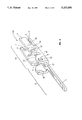
- FIG. 2 is a rear perspective view of a pin-receiving socket contact made in accordance with the preferred embodiment of the present invention.
- FIG. 3a is a top plan view of the mating region of the present invention shown prior to pin insertion.
- FIG. 3b is a top plan view of the mating region of the present invention shown after pin insertion.
- FIG. 4a is a top plan view of the preferred embodiment of the present invention shown after pin insertion.
- FIG. 4b is a side plan view of the preferred embodiment of the present invention shown after pin insertion.
- FIG. 5a is a cross-sectional view along line AA of FIG. 3a shown prior to pin insertion.
- FIG. 5b is a cross-sectional view along line AA of FIG. 4b shown after pin insertion.
- FIG. 6 is a top plan view of a socket contact blank illustrating the various methods of forming the preferred embodiment of the present invention.
- FIG. 7 is a top plan view of the preferred embodiment of the present invention shown on a carrier strip.
- FIG. 2 depicts an electrical socket contact utilizing the dimpled opposed cantilevered contact beams of the present invention.
- the socket contact consists of a mating region 10 and a retention region 9.
- the mating region 10 is formed of two opposed cantilevered contact beams 1, and 3 spaced apart by a spacing contact beam 2.
- the opposed contact beams 1, 3 are initially angled inward in a "flask” shaped arrangement and extend forward from the retention region 9 to a pin-receiving end 23.
- Both cantilevered contact beams 1, 3 and the spacing contact beam 3 are provided with an inwardly facing convex contact projection, or "dimple", 4, 6 and 5 (see FIG. 3a), respectively, adjacent the pin-receiving end 23.
- the maximum distance between the contact surfaces of the opposing dimples 4, 6 is less than the diameter or thickness of an electrical pin.
- Each mating beam 1, 2, 3 preferably has its dimple spaced a short distance from the pin-receiving end 23.
- Opposed contact beams 1 and 3 are initially biased inwardly towards each other along transition lines 21 and 22, respectively.
- a compliance slot 15 separates contact beams 2 and 3.
- a similar compliance slot 14 (not shown) separates contact beams 1 and 2.
- the compliance slots 14 and 15 define the contact beams 1, 2, and 3 and make the contact beams more compliant to pin insertions.
- the retention region 9 has a generally U-shaped configuration including a main section 17 integrally attached to a retention stake 7 extending outwardly from the retention region 9.
- a pair of spaced apart upstanding side legs 16, 18 extend approximately perpendicular to the main section 17 to an upper free end.
- Retention clips 20, 19 are attached to legs 16, 17, 18, respectively, and extend outwardly at angles acute to the planes defined by the main section 17 and legs 16, 18, ending at outer free ends.
- the retention region 9 retains the socket contact in a receptacle such as an insulating connector shell (not shown) for use in a printed wiring board or in a disk drive unit.
- the mating region 10 is separated from the retention region 9 by slots 11 and 12.
- the separation resulting from slots 11 and 12 isolates the function of the mating region 10 from the function of the retention region 9.
- the present invention facilitates pin insertions by providing a highly durable and reliable socket contact. More particularly, in the preferred embodiment shown in FIG. 3a, to insert a pin into the socket contact mating region 10, the insertion end of an electrical pin 13 is positioned adjacent the pin-receiving end 23.
- the contact beams 1, 2, and 3 have their dimples 4, 5, and 6, respectively, positioned such that when a pin 13 enters the pin-receiving end 23, the pin 13 first encounters the contact dimples. This configuration assists in prior pin alignment with the socket contact.
- the opposed contact beams 1, 3 are forced outwardly in a direction away from the inserted pin 13. Once the opposed contact beams 1, 3 are initially displaced, the pin 13 encounters only the contact dimples 4, 5, 6, embossed on each contact beam 1, 2, 3, respectively, and thus encounters only constant frictional forces from the contact dimples 4, 5, 6.
- This configuration reduces insertion forces and enhances the mechanical durability of the socket contact.
- FIG. 3b shows a top plan view of the socket contact mating region 10 with a pin 13 fully inserted.
- the opposed contact beams 1, 3 maintain constant contact with inserted pin 13 at contact dimples 4 and 6, respectively.
- Mechanical and electrical contact is maintained by virtue of the compression and torsional moments of opposed contact beams 1 and 3. More specifically, contact beam 1 produces a torsional moment about transition line 21 which exhibits a compressional force on dimple 4 normal to the sides of the pin 13. Similarly, contact beam 3 produces a torsional moment about transition line 22 which exhibits a compressional force on dimple 6 normal to the opposite side of the pin 13.
- the spacing contact beam 2 maintains electrical and mechanical contact with an inserted pin 13 via contact dimple 5. This configuration provides a redundant high normal force contact which is both mechanically and electrically reliable.
- FIG. 5a shows a cross-sectional view along line AA of FIG. 3a, prior to pin insertion.
- contact beams 1, 2, 3 form a flask shape, with opposing contact beams 1 and 3 initially angled inward towards each other.
- FIG. 5b shows a cross-sectional view along line AA after a pin 13 is inserted into the socket contact.
- the opposed contact beams 1 and 3 "roll" open from their original flask shape to a "U" shape so that the mating region 10 can accommodate the incoming pin.
- the resulting compression from the opposed contact beams 1 and 3 against the sides of the inserted pin 13 provides enhanced mechanical and electrical contact between the pin 13 and the socket contact.
- the socket contact blank is stamped from sheet metal stock.
- the main section 17 is stamped out of the stock at the same time that the retention stake 7 and contact beams 1, 2 and 3 are stamped and defined in the blank, and the contact dimples 4, 5, 6 are defined.
- the preferred embodiment is formed by folding the flat blank along fold lines 24 and 25 so that the retention legs 16 and 17 form a generally U-shaped configuration with the main section 17.
- the opposed contact beams 1, 3 are folded inwardly towards each other along transition lines 21 and 22, respectively, to form their initial flask shape.
- the preferred embodiment of the present invention is shown on a carrier strip as it would be used in a printed circuit board requiring 0.050 inch centerline spacing.
- the maximum distance between the outer periphery of the opposed contact beams 1 and 3 is 0.038 inches in order to fit within the confines a connector shell having 0.050 inch centerline space.
- the simple structure of the present invention permits a reduced cavity size of the socket contact, thereby enabling socket contacts to be spaced such that they can be used in printed circuit boards requiring tight centerline spacing.
- the independent opposed cantilevered, contact beams 1 and 3 of the inventive structure each with a contact dimple, provide efficient, reliable, and durable contact with an inserted pin 13 due to the torsional and bi-modal compressional moments of the opposed contact beams.
Abstract
Description
Claims (7)
Priority Applications (5)
| Application Number | Priority Date | Filing Date | Title |
|---|---|---|---|
| US07/677,778 US5151056A (en) | 1991-03-29 | 1991-03-29 | Electrical contact system with cantilever mating beams |
| EP19910312049 EP0505646A3 (en) | 1991-03-29 | 1991-12-27 | Electrical contact system with cantilever mating beams |
| KR1019920004484A KR920019015A (en) | 1991-03-29 | 1992-03-19 | Electrical socket contactor with cantilever matching beam |
| US07/854,208 US5237742A (en) | 1991-03-29 | 1992-03-20 | Method of producing electrical contact socket |
| JP4068965A JPH0582202A (en) | 1991-03-29 | 1992-03-27 | Electric contact system with cantilever insert beam and manufacture thereof |
Applications Claiming Priority (1)
| Application Number | Priority Date | Filing Date | Title |
|---|---|---|---|
| US07/677,778 US5151056A (en) | 1991-03-29 | 1991-03-29 | Electrical contact system with cantilever mating beams |
Related Child Applications (1)
| Application Number | Title | Priority Date | Filing Date |
|---|---|---|---|
| US07/854,208 Division US5237742A (en) | 1991-03-29 | 1992-03-20 | Method of producing electrical contact socket |
Publications (1)
| Publication Number | Publication Date |
|---|---|
| US5151056A true US5151056A (en) | 1992-09-29 |
Family
ID=24720084
Family Applications (1)
| Application Number | Title | Priority Date | Filing Date |
|---|---|---|---|
| US07/677,778 Expired - Fee Related US5151056A (en) | 1991-03-29 | 1991-03-29 | Electrical contact system with cantilever mating beams |
Country Status (4)
| Country | Link |
|---|---|
| US (1) | US5151056A (en) |
| EP (1) | EP0505646A3 (en) |
| JP (1) | JPH0582202A (en) |
| KR (1) | KR920019015A (en) |
Cited By (44)
| Publication number | Priority date | Publication date | Assignee | Title |
|---|---|---|---|---|
| US6024613A (en) * | 1997-10-31 | 2000-02-15 | Ddk, Ltd. | Socket contact and method for producing the same |
| US6190215B1 (en) | 1997-01-31 | 2001-02-20 | Berg Technology, Inc. | Stamped power contact |
| US20060148280A1 (en) * | 2005-01-05 | 2006-07-06 | Ashman John J | Angled compliant pin interconnector |
| US20080210015A1 (en) * | 2007-02-02 | 2008-09-04 | Shenzhen Futaihong Precision Industry Co., Ltd. | Failure analysis system and method using the same |
| WO2008147698A1 (en) * | 2007-05-21 | 2008-12-04 | Fci | Electrical connector with stress-distribution features |
| US7541135B2 (en) | 2005-04-05 | 2009-06-02 | Fci Americas Technology, Inc. | Power contact having conductive plates with curved portions contact beams and board tails |
| US7641500B2 (en) | 2007-04-04 | 2010-01-05 | Fci Americas Technology, Inc. | Power cable connector system |
| USD608293S1 (en) | 2009-01-16 | 2010-01-19 | Fci Americas Technology, Inc. | Vertical electrical connector |
| USD610548S1 (en) | 2009-01-16 | 2010-02-23 | Fci Americas Technology, Inc. | Right-angle electrical connector |
| US7690937B2 (en) | 2003-12-31 | 2010-04-06 | Fci Americas Technology, Inc. | Electrical power contacts and connectors comprising same |
| USRE41283E1 (en) | 2003-01-28 | 2010-04-27 | Fci Americas Technology, Inc. | Power connector with safety feature |
| US7726982B2 (en) | 2006-06-15 | 2010-06-01 | Fci Americas Technology, Inc. | Electrical connectors with air-circulation features |
| USD618181S1 (en) | 2009-04-03 | 2010-06-22 | Fci Americas Technology, Inc. | Asymmetrical electrical connector |
| USD618180S1 (en) | 2009-04-03 | 2010-06-22 | Fci Americas Technology, Inc. | Asymmetrical electrical connector |
| US7749009B2 (en) | 2005-01-31 | 2010-07-06 | Fci Americas Technology, Inc. | Surface-mount connector |
| USD619099S1 (en) | 2009-01-30 | 2010-07-06 | Fci Americas Technology, Inc. | Electrical connector |
| US7762857B2 (en) | 2007-10-01 | 2010-07-27 | Fci Americas Technology, Inc. | Power connectors with contact-retention features |
| US7775822B2 (en) | 2003-12-31 | 2010-08-17 | Fci Americas Technology, Inc. | Electrical connectors having power contacts with alignment/or restraining features |
| USD640637S1 (en) | 2009-01-16 | 2011-06-28 | Fci Americas Technology Llc | Vertical electrical connector |
| USD641709S1 (en) | 2009-01-16 | 2011-07-19 | Fci Americas Technology Llc | Vertical electrical connector |
| US20110248736A1 (en) * | 2010-04-09 | 2011-10-13 | Yamaichi Electronics Co., Ltd. | Probe pin and an ic socket with the same |
| US8062051B2 (en) | 2008-07-29 | 2011-11-22 | Fci Americas Technology Llc | Electrical communication system having latching and strain relief features |
| US20120077393A1 (en) * | 2009-05-19 | 2012-03-29 | Chul-Sub Lee | Connector For Low Profile Fuse |
| USD664096S1 (en) | 2009-01-16 | 2012-07-24 | Fci Americas Technology Llc | Vertical electrical connector |
| US8323049B2 (en) | 2009-01-30 | 2012-12-04 | Fci Americas Technology Llc | Electrical connector having power contacts |
| WO2013055557A1 (en) * | 2011-10-14 | 2013-04-18 | Delphi Technologies, Inc. | Tuning fork electrical contact with prongs having non-rectangular shape |
| JP2013196817A (en) * | 2012-03-16 | 2013-09-30 | Makita Corp | Terminal mechanism |
| USD718253S1 (en) | 2012-04-13 | 2014-11-25 | Fci Americas Technology Llc | Electrical cable connector |
| US8905651B2 (en) | 2012-01-31 | 2014-12-09 | Fci | Dismountable optical coupling device |
| USD720698S1 (en) | 2013-03-15 | 2015-01-06 | Fci Americas Technology Llc | Electrical cable connector |
| US8944831B2 (en) | 2012-04-13 | 2015-02-03 | Fci Americas Technology Llc | Electrical connector having ribbed ground plate with engagement members |
| USD727268S1 (en) | 2012-04-13 | 2015-04-21 | Fci Americas Technology Llc | Vertical electrical connector |
| USD727852S1 (en) | 2012-04-13 | 2015-04-28 | Fci Americas Technology Llc | Ground shield for a right angle electrical connector |
| US9048583B2 (en) | 2009-03-19 | 2015-06-02 | Fci Americas Technology Llc | Electrical connector having ribbed ground plate |
| USD733662S1 (en) | 2013-01-25 | 2015-07-07 | Fci Americas Technology Llc | Connector housing for electrical connector |
| US9112292B2 (en) | 2012-03-16 | 2015-08-18 | Makita Corporation | Terminal structure |
| USD746236S1 (en) | 2012-07-11 | 2015-12-29 | Fci Americas Technology Llc | Electrical connector housing |
| US9257778B2 (en) | 2012-04-13 | 2016-02-09 | Fci Americas Technology | High speed electrical connector |
| US9265150B2 (en) | 2014-02-14 | 2016-02-16 | Lear Corporation | Semi-compliant terminals |
| US9543703B2 (en) | 2012-07-11 | 2017-01-10 | Fci Americas Technology Llc | Electrical connector with reduced stack height |
| WO2017014751A1 (en) * | 2015-07-21 | 2017-01-26 | Hewlett-Packard Development Company, L.P. | Female electrical terminals |
| US10312621B2 (en) * | 2017-07-20 | 2019-06-04 | Yazaki Corporation | Terminal connection structure |
| US10411420B2 (en) | 2015-04-30 | 2019-09-10 | Schneider Electric Industries Sas | Universal electrical installation system |
| US11888251B2 (en) | 2021-03-31 | 2024-01-30 | Te Connectivity Germany Gmbh | Contact element for an electrical plug |
Families Citing this family (1)
| Publication number | Priority date | Publication date | Assignee | Title |
|---|---|---|---|---|
| JP2006066384A (en) * | 2004-07-27 | 2006-03-09 | Hosiden Corp | Coaxial connector for board-to-board connection |
Citations (3)
| Publication number | Priority date | Publication date | Assignee | Title |
|---|---|---|---|---|
| US4717361A (en) * | 1985-08-02 | 1988-01-05 | Daiichi Denshi Kogyo Kabushiki Kaisha | Contact for connector |
| US4877409A (en) * | 1988-01-22 | 1989-10-31 | Amp Incorporated | Hinged electrical connector |
| US5007865A (en) * | 1987-09-28 | 1991-04-16 | Amp Incorporated | Electrical receptacle terminal |
Family Cites Families (4)
| Publication number | Priority date | Publication date | Assignee | Title |
|---|---|---|---|---|
| FR960968A (en) * | 1950-04-28 | |||
| BE631920A (en) * | 1962-05-17 | |||
| US4007977A (en) * | 1974-05-09 | 1977-02-15 | Bunker Ramo Corporation | Electrical connector |
| EP0218325B1 (en) * | 1985-09-30 | 1992-11-11 | Molex Incorporated | Pin-receiving terminal |
-
1991
- 1991-03-29 US US07/677,778 patent/US5151056A/en not_active Expired - Fee Related
- 1991-12-27 EP EP19910312049 patent/EP0505646A3/en not_active Withdrawn
-
1992
- 1992-03-19 KR KR1019920004484A patent/KR920019015A/en not_active Application Discontinuation
- 1992-03-27 JP JP4068965A patent/JPH0582202A/en active Pending
Patent Citations (3)
| Publication number | Priority date | Publication date | Assignee | Title |
|---|---|---|---|---|
| US4717361A (en) * | 1985-08-02 | 1988-01-05 | Daiichi Denshi Kogyo Kabushiki Kaisha | Contact for connector |
| US5007865A (en) * | 1987-09-28 | 1991-04-16 | Amp Incorporated | Electrical receptacle terminal |
| US4877409A (en) * | 1988-01-22 | 1989-10-31 | Amp Incorporated | Hinged electrical connector |
Cited By (73)
| Publication number | Priority date | Publication date | Assignee | Title |
|---|---|---|---|---|
| US6190215B1 (en) | 1997-01-31 | 2001-02-20 | Berg Technology, Inc. | Stamped power contact |
| US6024613A (en) * | 1997-10-31 | 2000-02-15 | Ddk, Ltd. | Socket contact and method for producing the same |
| USRE41283E1 (en) | 2003-01-28 | 2010-04-27 | Fci Americas Technology, Inc. | Power connector with safety feature |
| US8187017B2 (en) | 2003-12-31 | 2012-05-29 | Fci Americas Technology Llc | Electrical power contacts and connectors comprising same |
| US7775822B2 (en) | 2003-12-31 | 2010-08-17 | Fci Americas Technology, Inc. | Electrical connectors having power contacts with alignment/or restraining features |
| US7862359B2 (en) | 2003-12-31 | 2011-01-04 | Fci Americas Technology Llc | Electrical power contacts and connectors comprising same |
| US7690937B2 (en) | 2003-12-31 | 2010-04-06 | Fci Americas Technology, Inc. | Electrical power contacts and connectors comprising same |
| US8062046B2 (en) | 2003-12-31 | 2011-11-22 | Fci Americas Technology Llc | Electrical power contacts and connectors comprising same |
| US7077658B1 (en) | 2005-01-05 | 2006-07-18 | Avx Corporation | Angled compliant pin interconnector |
| US20060148280A1 (en) * | 2005-01-05 | 2006-07-06 | Ashman John J | Angled compliant pin interconnector |
| US7749009B2 (en) | 2005-01-31 | 2010-07-06 | Fci Americas Technology, Inc. | Surface-mount connector |
| US7541135B2 (en) | 2005-04-05 | 2009-06-02 | Fci Americas Technology, Inc. | Power contact having conductive plates with curved portions contact beams and board tails |
| US7726982B2 (en) | 2006-06-15 | 2010-06-01 | Fci Americas Technology, Inc. | Electrical connectors with air-circulation features |
| US20080210015A1 (en) * | 2007-02-02 | 2008-09-04 | Shenzhen Futaihong Precision Industry Co., Ltd. | Failure analysis system and method using the same |
| US7641500B2 (en) | 2007-04-04 | 2010-01-05 | Fci Americas Technology, Inc. | Power cable connector system |
| US7905731B2 (en) | 2007-05-21 | 2011-03-15 | Fci Americas Technology, Inc. | Electrical connector with stress-distribution features |
| WO2008147698A1 (en) * | 2007-05-21 | 2008-12-04 | Fci | Electrical connector with stress-distribution features |
| US7762857B2 (en) | 2007-10-01 | 2010-07-27 | Fci Americas Technology, Inc. | Power connectors with contact-retention features |
| US8062051B2 (en) | 2008-07-29 | 2011-11-22 | Fci Americas Technology Llc | Electrical communication system having latching and strain relief features |
| USD696199S1 (en) | 2009-01-16 | 2013-12-24 | Fci Americas Technology Llc | Vertical electrical connector |
| USD640637S1 (en) | 2009-01-16 | 2011-06-28 | Fci Americas Technology Llc | Vertical electrical connector |
| USD641709S1 (en) | 2009-01-16 | 2011-07-19 | Fci Americas Technology Llc | Vertical electrical connector |
| USD647058S1 (en) | 2009-01-16 | 2011-10-18 | Fci Americas Technology Llc | Vertical electrical connector |
| USD660245S1 (en) | 2009-01-16 | 2012-05-22 | Fci Americas Technology Llc | Vertical electrical connector |
| USD610548S1 (en) | 2009-01-16 | 2010-02-23 | Fci Americas Technology, Inc. | Right-angle electrical connector |
| USD651981S1 (en) | 2009-01-16 | 2012-01-10 | Fci Americas Technology Llc | Vertical electrical connector |
| USD664096S1 (en) | 2009-01-16 | 2012-07-24 | Fci Americas Technology Llc | Vertical electrical connector |
| USD608293S1 (en) | 2009-01-16 | 2010-01-19 | Fci Americas Technology, Inc. | Vertical electrical connector |
| USD619099S1 (en) | 2009-01-30 | 2010-07-06 | Fci Americas Technology, Inc. | Electrical connector |
| US8323049B2 (en) | 2009-01-30 | 2012-12-04 | Fci Americas Technology Llc | Electrical connector having power contacts |
| US10720721B2 (en) | 2009-03-19 | 2020-07-21 | Fci Usa Llc | Electrical connector having ribbed ground plate |
| US9048583B2 (en) | 2009-03-19 | 2015-06-02 | Fci Americas Technology Llc | Electrical connector having ribbed ground plate |
| US10096921B2 (en) | 2009-03-19 | 2018-10-09 | Fci Usa Llc | Electrical connector having ribbed ground plate |
| US9461410B2 (en) | 2009-03-19 | 2016-10-04 | Fci Americas Technology Llc | Electrical connector having ribbed ground plate |
| USD653621S1 (en) | 2009-04-03 | 2012-02-07 | Fci Americas Technology Llc | Asymmetrical electrical connector |
| USD618181S1 (en) | 2009-04-03 | 2010-06-22 | Fci Americas Technology, Inc. | Asymmetrical electrical connector |
| USD618180S1 (en) | 2009-04-03 | 2010-06-22 | Fci Americas Technology, Inc. | Asymmetrical electrical connector |
| US20120077393A1 (en) * | 2009-05-19 | 2012-03-29 | Chul-Sub Lee | Connector For Low Profile Fuse |
| US8668532B2 (en) * | 2009-05-19 | 2014-03-11 | Tyco Electronics Amp Korea Ltd. | Connector for low profile fuse |
| US20110248736A1 (en) * | 2010-04-09 | 2011-10-13 | Yamaichi Electronics Co., Ltd. | Probe pin and an ic socket with the same |
| US8669774B2 (en) * | 2010-04-09 | 2014-03-11 | Yamaichi Electronics Co., Ltd. | Probe pin and an IC socket with the same |
| US8556666B2 (en) | 2011-10-14 | 2013-10-15 | Delphi Technologies, Inc. | Tuning fork electrical contact with prongs having non-rectangular shape |
| WO2013055557A1 (en) * | 2011-10-14 | 2013-04-18 | Delphi Technologies, Inc. | Tuning fork electrical contact with prongs having non-rectangular shape |
| CN103947048A (en) * | 2011-10-14 | 2014-07-23 | 德尔福技术有限公司 | Tuning fork electrical contact with prongs having non-rectangular shape |
| CN103947048B (en) * | 2011-10-14 | 2016-08-24 | 德尔福技术有限公司 | There is tuning-fork type electric contact piece and the manufacture method thereof of non-rectangle prong |
| US8905651B2 (en) | 2012-01-31 | 2014-12-09 | Fci | Dismountable optical coupling device |
| US9112292B2 (en) | 2012-03-16 | 2015-08-18 | Makita Corporation | Terminal structure |
| JP2013196817A (en) * | 2012-03-16 | 2013-09-30 | Makita Corp | Terminal mechanism |
| USD750025S1 (en) | 2012-04-13 | 2016-02-23 | Fci Americas Technology Llc | Vertical electrical connector |
| USD816044S1 (en) | 2012-04-13 | 2018-04-24 | Fci Americas Technology Llc | Electrical cable connector |
| US8944831B2 (en) | 2012-04-13 | 2015-02-03 | Fci Americas Technology Llc | Electrical connector having ribbed ground plate with engagement members |
| US9831605B2 (en) | 2012-04-13 | 2017-11-28 | Fci Americas Technology Llc | High speed electrical connector |
| USD748063S1 (en) | 2012-04-13 | 2016-01-26 | Fci Americas Technology Llc | Electrical ground shield |
| US9257778B2 (en) | 2012-04-13 | 2016-02-09 | Fci Americas Technology | High speed electrical connector |
| USD790471S1 (en) | 2012-04-13 | 2017-06-27 | Fci Americas Technology Llc | Vertical electrical connector |
| USD750030S1 (en) | 2012-04-13 | 2016-02-23 | Fci Americas Technology Llc | Electrical cable connector |
| USD718253S1 (en) | 2012-04-13 | 2014-11-25 | Fci Americas Technology Llc | Electrical cable connector |
| USD727268S1 (en) | 2012-04-13 | 2015-04-21 | Fci Americas Technology Llc | Vertical electrical connector |
| USD727852S1 (en) | 2012-04-13 | 2015-04-28 | Fci Americas Technology Llc | Ground shield for a right angle electrical connector |
| USD746236S1 (en) | 2012-07-11 | 2015-12-29 | Fci Americas Technology Llc | Electrical connector housing |
| USD751507S1 (en) | 2012-07-11 | 2016-03-15 | Fci Americas Technology Llc | Electrical connector |
| US9871323B2 (en) | 2012-07-11 | 2018-01-16 | Fci Americas Technology Llc | Electrical connector with reduced stack height |
| US9543703B2 (en) | 2012-07-11 | 2017-01-10 | Fci Americas Technology Llc | Electrical connector with reduced stack height |
| USD733662S1 (en) | 2013-01-25 | 2015-07-07 | Fci Americas Technology Llc | Connector housing for electrical connector |
| USD766832S1 (en) | 2013-01-25 | 2016-09-20 | Fci Americas Technology Llc | Electrical connector |
| USD745852S1 (en) | 2013-01-25 | 2015-12-22 | Fci Americas Technology Llc | Electrical connector |
| USD772168S1 (en) | 2013-01-25 | 2016-11-22 | Fci Americas Technology Llc | Connector housing for electrical connector |
| USD720698S1 (en) | 2013-03-15 | 2015-01-06 | Fci Americas Technology Llc | Electrical cable connector |
| US9265150B2 (en) | 2014-02-14 | 2016-02-16 | Lear Corporation | Semi-compliant terminals |
| US10411420B2 (en) | 2015-04-30 | 2019-09-10 | Schneider Electric Industries Sas | Universal electrical installation system |
| WO2017014751A1 (en) * | 2015-07-21 | 2017-01-26 | Hewlett-Packard Development Company, L.P. | Female electrical terminals |
| US10312621B2 (en) * | 2017-07-20 | 2019-06-04 | Yazaki Corporation | Terminal connection structure |
| US11888251B2 (en) | 2021-03-31 | 2024-01-30 | Te Connectivity Germany Gmbh | Contact element for an electrical plug |
Also Published As
| Publication number | Publication date |
|---|---|
| JPH0582202A (en) | 1993-04-02 |
| EP0505646A3 (en) | 1993-03-31 |
| KR920019015A (en) | 1992-10-22 |
| EP0505646A2 (en) | 1992-09-30 |
Similar Documents
| Publication | Publication Date | Title |
|---|---|---|
| US5151056A (en) | Electrical contact system with cantilever mating beams | |
| US6033245A (en) | Self-aligning electrical connector | |
| JP2609114B2 (en) | Contact socket | |
| US4416504A (en) | Contact with dual cantilevered arms with narrowed, complimentary tip portions | |
| US5588884A (en) | Stamped and formed contacts for a power connector | |
| US5653616A (en) | Electrical receptacle terminal | |
| US5188545A (en) | Electrical socket terminal | |
| US5145386A (en) | Low profile electrical connector | |
| JP4650918B2 (en) | Electrical connector | |
| EP1120861A2 (en) | Electrical connector having an improved female contact | |
| JPH06260248A (en) | Low insertion power electric connector | |
| JP3428756B2 (en) | Female electrical terminal | |
| US6056604A (en) | Electrical receptacle terminal with a contact spring biased against a side of the receptacle without spreading a seam in the side of the receptacle | |
| JP2631258B2 (en) | Male electrical terminal having excessive stress prevention means | |
| US5462459A (en) | Spring-type electrical receptacle | |
| JPH0415996B2 (en) | ||
| EP0542068B1 (en) | Female electrical contact | |
| US5237742A (en) | Method of producing electrical contact socket | |
| US5015200A (en) | Connector with double acting latch | |
| JP3143222U (en) | Connector with improved dual beam contact | |
| US20020173190A1 (en) | Self-aligning power connector system | |
| JP3067545B2 (en) | Female terminal fitting | |
| EP0261839B1 (en) | Spring contact electrical connector assembly | |
| US5556306A (en) | Stamped cantilever contact having closed-type engagement portion | |
| EP0268356B1 (en) | Electrical receptacle |
Legal Events
| Date | Code | Title | Description |
|---|---|---|---|
| AS | Assignment |
Owner name: ELCO CORPORATION, A CORPORATION OF PA, PENNSYLVANI Free format text: ASSIGNMENT OF ASSIGNORS INTEREST.;ASSIGNOR:MCCLUNE, DONALD W.;REEL/FRAME:005815/0585 Effective date: 19910429 |
|
| FPAY | Fee payment |
Year of fee payment: 4 |
|
| FEPP | Fee payment procedure |
Free format text: PAYOR NUMBER ASSIGNED (ORIGINAL EVENT CODE: ASPN); ENTITY STATUS OF PATENT OWNER: LARGE ENTITY |
|
| FEPP | Fee payment procedure |
Free format text: PAYOR NUMBER ASSIGNED (ORIGINAL EVENT CODE: ASPN); ENTITY STATUS OF PATENT OWNER: LARGE ENTITY |
|
| FEPP | Fee payment procedure |
Free format text: PAYER NUMBER DE-ASSIGNED (ORIGINAL EVENT CODE: RMPN); ENTITY STATUS OF PATENT OWNER: LARGE ENTITY |
|
| FPAY | Fee payment |
Year of fee payment: 8 |
|
| REMI | Maintenance fee reminder mailed | ||
| LAPS | Lapse for failure to pay maintenance fees | ||
| FP | Lapsed due to failure to pay maintenance fee |
Effective date: 20040929 |
|
| STCH | Information on status: patent discontinuation |
Free format text: PATENT EXPIRED DUE TO NONPAYMENT OF MAINTENANCE FEES UNDER 37 CFR 1.362 |