US5146357A - Data communications system that prevents undesired coupling between data stations - Google Patents
Data communications system that prevents undesired coupling between data stations Download PDFInfo
- Publication number
- US5146357A US5146357A US07/519,442 US51944290A US5146357A US 5146357 A US5146357 A US 5146357A US 51944290 A US51944290 A US 51944290A US 5146357 A US5146357 A US 5146357A
- Authority
- US
- United States
- Prior art keywords
- optical
- data
- data signal
- metallic line
- power source
- Prior art date
- Legal status (The legal status is an assumption and is not a legal conclusion. Google has not performed a legal analysis and makes no representation as to the accuracy of the status listed.)
- Expired - Fee Related
Links
Images


Classifications
-
- H—ELECTRICITY
- H04—ELECTRIC COMMUNICATION TECHNIQUE
- H04B—TRANSMISSION
- H04B10/00—Transmission systems employing electromagnetic waves other than radio-waves, e.g. infrared, visible or ultraviolet light, or employing corpuscular radiation, e.g. quantum communication
- H04B10/80—Optical aspects relating to the use of optical transmission for specific applications, not provided for in groups H04B10/03 - H04B10/70, e.g. optical power feeding or optical transmission through water
- H04B10/801—Optical aspects relating to the use of optical transmission for specific applications, not provided for in groups H04B10/03 - H04B10/70, e.g. optical power feeding or optical transmission through water using optical interconnects, e.g. light coupled isolators, circuit board interconnections
- H04B10/802—Optical aspects relating to the use of optical transmission for specific applications, not provided for in groups H04B10/03 - H04B10/70, e.g. optical power feeding or optical transmission through water using optical interconnects, e.g. light coupled isolators, circuit board interconnections for isolation, e.g. using optocouplers
Definitions
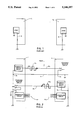
- the present invention relates to the general art of data communications, and to the particular field of accurate directly coupled long distance data communication.
- each such computer C 1 and C N was, and still is, wired to a local ground where it is plugged into a source of power.
- a ground level lead GL travels throughout all of the computer logic and is at ground potential of a local ground.
- Peripheral equipment such as terminals, printers, and the like, have their logic grounded in the same manner.
- RS232 A common means of connecting such units was, and still is, RS232 as indicated in FIG. 2.
- one metallic conductor M 1 takes data signals DS 1 from unit T to unit R
- a second metallic conductor M 2 takes data signals DS 2 from unit R back to unit T
- Still another metallic conductor G 1 ties the ground G T of the unit T to the ground G R of the unit R.
- units T and R shown in FIG. 2 include other control leads CL T and CL R for "handshaking".
- the handshaking terminal of one unit will "ask" a corresponding handshaking terminal of a second unit if that second unit is ready to receive data signals, indicate that the terminal is on, and then wait for a return signal to indicate readiness.
- the first terminal Upon receipt of a ready signal, the first terminal transmits data signals to the second terminal. Similar kissoff signals and sequences are used at the completion of a data signal transmission.
- RS232 While successful, RS232 still has several drawbacks.
- One such drawback is a limit of about fifty feet for an RS232 connection. If the connection exceeds fifty feet, there is a possibility of a degradation of speed and accuracy of data transfer. Furthermore, there may even be a possibility that hardware can be damaged. Still another problem which can arise if RS232 exceeds fifty feet is a possible increase in erratic operation. Often erratic operation problems manifest in errors that look like disc or CPU errors which are not associated with communications, so a user may waste time and money looking for an error in the wrong place.
- RS422 was developed. RS422 is shown in FIG. 3, and adds a mirror image signal DS 1M and DS 2M , in each direction. The transmitted data signal thus becomes a differential pair and can be received more accurately. In design concept, the receiving unit merely needs to look at the difference between the two lines M 1 and M 1M or M 2 and M 2M to determine if a "1" or a "0" has been transmitted.
- ground wire G used in RS232 and in RS422 has been a source of the errors commonly associated with these connections.
- the ground lead G ties the grounds G T and G R together.
- ground level potential associated with one unit, such as unit T may be different from that ground level potential associated with another unit, such as unit R. This is especially the case if lightning strikes in the vicinity of the connection or of either unit. Switching of adjacent electrical equipment may also disturb a local ground.
- ground level potential difference may even generate a voltage potential.
- any differences in ground potential are generally spread out evenly across the logic of a unit.
- this difference may be spread out across the logic of all of the units connected by the ground leads, such as ground lead G.
- ground leads such as ground lead G. The inventor has found that such ground coupling can lead to miscellaneous errors and even hardware damage.
- data signals are generally transmitted and received by two tiny, generally inexpensive, chips called line drivers and receivers.
- the line receiver "receives" both the minute data voltage and the ground voltage. If the ground voltage is large, it may be larger than the data signal, and can thus cause errors in data transmission. Since a metallic ground path violates the integrity of a CPU, memory or disc, even if the unit is turned off, errors can occur. Still further, even in the case of the RS422, the ground wire coupling of units can still create the above-mentioned problems. The problems are exacerbated if voltage spikes or the like are induced in the ground lead.
- the inventor has also found that even if elements such as modems, ground isolation elements and the like are used in each element, due to the existence of this ground coupling of the units, the problem still exists.
- any disturbance in such power may find its way to the equipment coupled to the connection lead.
- It is a main object of the present invention is to provide a data communications transceiver which prevents undesired coupling between data stations.
- a data communications transceiver which totally isolates the ground circuit of each unit to which a data communications line is connected from that data communications line.
- the isolation is achieved by using optical coupling to couple the line to the unit, and establishing a physical gap between the line and the unit.
- the optical coupler is powered by a power source which is totally separate from the power source of any unit to which the data communications line is connected, and can be further protected using special power filtering and surge suppressor elements.
- the gap is sized so that a lightning strike will not bridge that gap.
- the system further uses a truly balanced line receiver in which the only component connected to the receiving end of the connecting cable is an optical source which is optically connected to a photodetector.
- the source will simply turn on and off depending on the current flow in the line, and electrical common mode noise in the line will not influence the coupling.
- the optical coupler can be viewed as a perfect differential digital receiver.
- the advantage of fiber optic communications can be realized to prevent the ground path of one unit from being electrically coupled to the ground path of another unit via a ground line of a connecting line.
- optical coupler of the present invention is used in conjunction with a metallic line conductor so that expensive retrofitting of an existing system with fiber optic cables is avoided.
- optical coupler which has a power source that is totally isolated from the power sources associated with any units in the system results in advantages of fiber optic isolation along with an increase in data transmission speed and accuracy as well as an elimination of communication errors associated with a totally metallic path from one unit to another.
- FIG. 1 illustrates a prior art setup which includes two stand alone units.
- FIG. 2 illustrates a prior art setup in which two units are connected by an RS232 line conductor to facilitate the transfer of data from one unit to another.
- FIG. 3 illustrates a prior art setup in which two units are connected by an RS422 line conductor to facilitate the transfer of data from one unit to another.
- FIG. 4 illustrates the present invention in which an optical coupler is used to connect a metallic line conductor to an associated unit so that the ground path of each unit is separated from the conductor and from any other unit in the system.
- FIG. 5 illustrates the present invention in which mirror image differential signals are used to amplify a data signal, and in which a true balanced line receiver is established.
- FIG. 6 illustrates the present invention in which various signal conditioning elements are included.
- FIG. 7 illustrates the present invention in which signal integrity and polarity can be checked at various points along a long data communications line, and which includes power surge protectors on the data communications line.
- FIG. 8 shows a circuit diagram of the data communications transceiver of the present invention.
- FIG. 9 shows multiplexer logic that can be used in conjunction with the transceiver of the present invention.
- FIG. 10 shows the transceiver of the present invention being used as a repeater for a long data line.
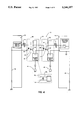
- FIG. 4 illustrates a data communications transceiver configuration 10 embodying the present invention.
- the configuration or transceiver 10 includes a plurality of separate units, such as computers, printers, displays and the like which send data signals back and forth to each other.
- the configuration 10 will be considered as including a transmitting station 12 which generates and transmits data signals, such as data signal 14 for use by a receiving station 16.
- Each of the units in the system has a power connection and a ground circuit which includes a ground lead, such as ground leads 18 and 20 in units 12 and 16 respectively which communicates with nearly all of the logic elements of the unit.
- the present invention couples these two units 12 and 16 in a manner such that the ground circuits of the two coupled units are not connected and are totally separate from each other, yet in a manner which permits accurate high speed data signal transmission over long distances, yet does not require major changes in the two units.
- the configuration 10 includes a metallic line conductor 22 over which data signal 14 travels from transmitting station 12 to receiving station 16 and which can be well over fifty feet in length.
- the configuration 10 further includes an optical coupling means which optically couples the metallic line conductor to the transmitter station and to the receiving station.
- the optical coupling means includes a first optical coupler 26 connecting one end of the metallic line conductor 22 to the transmitting station and a second optical coupler 28 connecting the other end of the metallic line conductor to the receiving station.
- the optical couplings 26 and 28 break any electrical path between the stations and the metallic line conductor.
- Each optical coupling includes an optical source and a photodetector and the appropriate signal conditioning equipment to translate the electrical signals generated by the stations into optical signals.
- the optical coupler 26 includes a transmitter optical source 30 connected to the transmitter station in a manner such that data signal 14 from the transmitter station is emitted by the optical source 30 as an optical signal 14' and a line conductor photodetector 32 which is connected to the metallic line conductor and which is located to receive the optical signal 14'.
- Appropriate equipment is associated with the photodetector 32 to translate the electrical signal 14' back into a signal that is appropriate to the metallic line conductor, and that signal is then transmitted along the line conductor to the other end thereof.
- the optical coupler 28 includes a line conductor optical source 36 which is connected to the line conductor via appropriate circuitry and which generates an optical signal 14" which corresponds to the data signals 14 and 14'.
- the optical coupler 28 further includes a receiver photodetector 38 which is connected to the receiver station 16 via appropriate circuitry to translate the optical signal 14" back into a data signal appropriate to the receiver station 16.
- Each photodetector of the optical coupling means is physically spaced apart from the adjacent optical source to define a gap, such as gaps 40 and 42 in optical couplings 26 and 28 respectively.
- gaps are sized so that a potential difference thereacross which is associated with a lightning strike will not cause a spark to jump the gap.
- the gaps can be sized so that a potential difference of approximately seven thousand volts thereacross will not cause a spark to jump the gap.
- the optical couplings 26 and 28 are the sole connection between the metallic line conductor 22 and the transmitting and receiving stations, and thus there is no electrical path between the ground circuits of these two stations.
- the optical couplings 26 and 28 are powered from a suitable power source means, with plug elements 44 and 46 being associated with the optical couplers 26 and 28 respectively.
- the power source means associated with the optical coupling means is totally separate from the power sources of the units, such as transmitting station 12 and receiving station 16, which are totally separate from each other. In this manner, there is no possibility that a ground path may be established between the ground circuit of any of these assemblies 12, 16, 22, 26 or 28.
- the plug element 44 can be associated with a capacitor CP that is connected to the power for unit 12 via a switch SP1 and is connected to the plug element via a switch SP2.
- the switch SP1 is closed to charge the capacitor, and when switch SP1 is closed, switch SP2 is open.
- the line can be powered from the capacitor by opening switch SP1 and closing switch SP2.
- FIG. 4 shows the capacitor associated with plug 44 and unit 12, a similar capacitor and switch combination can be associated with the plug 46 and the unit 16.
- optical sources and the photodetectors can be any of those elements known to those skilled in the art and are fully disclosed in standard textbooks such as “Fiber Optics Handbook for Engineers and Principles” by Frederick C. Allard and published by McGraw-Hill Publishing Company in 1990, the disclosure of which is incorporated herein by reference, or catalogs such as “Optoelectronics Data Book” published by TRW Company in 1986, especially product bulletin number 5246, dated January 1985 and appearing in Section E thereof, the disclosure of which is incorporated herein by reference.
- the optical source can be selected from any of a number of LED type elements, or any of a number of laser diodes or the like.
- the photodetectors can also be selected from any number of pn and PIN photodetectors, avalanche photodetectors, or the like as is also discussed in the referenced textbook and catalog. Again, circuit elements appropriate to such detectors is discussed in the referenced textbook, and attention is directed thereto.
- the configuration 10' is shown to include a balanced line concept in which common mode disturbances will not create errors in the transmitted data signals, and so the receiving end may always accurately mirror the polarity of the transmitted signal.
- the configuration 10' uses a mirror image type of transmission pattern in which an algebraic sum of two signals is used to form a final data signal.
- the configuration 10' includes two metallic line conductors 22' and 22" which have line photodetectors 32' and 32" and phototransmitters 30' and 30" thereon in position to receive optical signals from transmitter optical source 30. As is indicated in FIG.
- Such summing will be totally immune to common mode noise on the lines 22' and 22" as there is a simple addition of signals without reference to any ground signal so common mode noise or common mode disturbances will totally cancel out.
- the mirror image combinations will also increase the accuracy of the received signal, and represents a balance pair of a truly balanced line receiver. There is no ground connection and thus the above-discussed balanced pair occurs.
- data signals can be transmitted from the receiver station 16 back to the transmitting station 12 via a second setup 10' 2 that operates and functions in a manner similar to that just described in relation to the line conductors 22' and 22".
- a second setup 10' 2 that operates and functions in a manner similar to that just described in relation to the line conductors 22' and 22".
- multiple circuits may be added. These multiple circuits can be designed to use one common return path to reduce the total number of conductors and maintain the advantages defined herein.
- Both setups will include appropriate power means as indicated at 44 and 46 in FIG. 5.
- the transmitting station and the receiving station have multiple signal lines 50T and 50R which are also connected to the optical coupling means so that signals associated with these lines will also be transmitted via the optical coupling means.
- they may be jumped or provided with fixed polarities as required. They may also provide power to the device side circuitry.
- differential drivers and receivers also allows the receiving end to always be a mirror image of the transmitting end without possibility of ambiguity with regard to polarity and also allows higher speed performance. This is because the current on the communication circuit is always driven negative or positive to immediately correspond to the transmitted polarity.
- the configuration is shown to include suitable circuit means, such as inductor lights, multiplexers, driver stages, coders, "OR”ing diodes, and the like as indicated by blocks 52.
- signal conditioning means 54 can be associated with each station, and such signal conditioning means can include amplifiers and the like.
- the optical sources are also shown in FIG. 6 to include two LEDs 58 and 60 which are connected to emit an optical signal according to the direction of current in the signal line so that diode 58 emits an optical signal 14P when the signal 14 is positive and diode 60 emits an optical signal 14N when signal 14 is negative.
- the signals 14P and 14N are incident on photodetectors 32P and 32N respectively, and re-emitted as optical signals 14P' and 14N' by optical sources 36P and 36N respectively.
- the signals 36P and 36N are incident on the multiple receiver photodetector in element 38, one for negative and one for positive current.
- a data signal from the receiver station to the transmitter station is transmitted in a similar manner. Power is supplied to the optical coupling means by connectors 44 and 46 and similar connectors in the manner discussed above so that the line conductors and optical coupling means are all separate and independent of any ground circuit in the stations, such as transmitter station and receiver station.
- the circuit elements 52 and 54 can include circuit means for relaying digital data signals as well as driver circuits and the like associated with such data signals. Those skilled in the art will be able to determine exactly what elements are necessary to accomplish such results based on the teaching of textbooks such as the referenced Fiber Optics text, or the TRW catalog, as well as others.
- FIG. 7 Shown in FIG. 7 is are configurations 10" and 10"', both of which includes an integrity and polarity checking means on the line conductors and on the receiving station signal receiving lines, as well as surge protection means on the optical coupling means power source means.
- integrity and polarity checking means on the line conductors and on the receiving station signal receiving lines, as well as surge protection means on the optical coupling means power source means.
- surge protection means on the optical coupling means power source means.
- the integrity and polarity checking means includes a signal circuit 62 on the line conductor and a signal circuit 64 on the receiver station.
- Each signal circuit includes an optical source, such as an LED 66 connected to emit an optical signal R when current in the line conductor is in one direction and a second LED 68 connected to emit an optical signal G when current in the line conductor is in the opposite direction.
- the emitted optical signals can be conducted by a fiber optic cable 70 to a suitable viewing location.
- the associated signal circuit 64 includes an LED 72 which emits optical signal R' when the data signal is in one direction and optical signal G' when the data signal is in the opposite direction.
- the signals R' and G' correspond to the signals R and G so that a polarity and integrity check can be made.
- one circuit means 62 is located adjacent to the transmitting station and one circuit means 64 is located adjacent to the receiving station. However, there can be several circuit means 62 placed at various locations along the line conductor if necessary. Appropriate resistors can be included in the circuit means 62 and 64 to ensure that undue amounts of power are not tapped off by such circuit means.
- Each of the configurations 10" and 10"' also includes surge suppressors 76 on the power source means associated with the optical coupling means.
- surge suppressors can include an MOV (Metal Oxide Variator) element 76M, capacitors 76C and inductors, such as inductor 76L, as well as an inductor in the line as indicated at L in element 44S.
- MOV Metal Oxide Variator
- Other suppressor elements, such as capacitors or the like can be inserted in the line adjacent to the inductor L if suitable.
- An uninterruptible power supply U can also be included in the power source, one example of a suitable uninterruptible power supply is disclosed in U.S. Pat. No. 4,675,538, the disclosure of which is incorporated herein by reference.
- FIG. 10 The use of an uninterruptible power supply is indicated in FIG. 10.
- a first computer FC with an uninterruptible power supply U communicates with a second computer SC having its own uninterruptible power supply U2.
- the data line can be as much as two miles long, and the configuration network TR of the present invention including its own uninterruptible power supply can be inserted into the long data line and function as a repeater.
- the configuration network TR can also include an integral battery backup to continue critical communications in case of a blackout at the repeater location.
- FIG. 9 shows multiplexer logic that can be used in conjunction with the configuration of the present invention.
- multiplexers M and demultiplexers D can be included to allow multiple lower speed data circuits, such as data circuit D which includes a plurality of 1200 baud lines, to be merged into a higher speed data stream, such as 4800 baud line BL over the long distance data circuit and then separated at the receiving end to a multiplicity of stations.
- the configuration can also be used in party line voting or polling arrangements if desired.
- a modification of the optical coupling means includes circuit means 80 which develops a timing signal or strobe signal which could, for example, be based upon "dark” time when neither optical source 36 is turned on. Such "dark” time occurs when the data signal is switching states from positive to negative, and the circuit means 80 will be designed to operate until the voltage is large enough to exceed the forward breakdown voltage of the optical source.
- circuit means 82 which is "transparent" on start up or after a power failure so that the circuit does not lock up because the initialization of control leads on a computer side may not be in the sequence expected by a computer after such an occurrence.
- circuit elements can include, if suitable, means for defining a dead zone or threshold, and would be used in conjunction with the optical sources.
- This circuit would include a timing signal or a strobe signal that is based on dark time when none of the optical sources are emitting an optical signal. This circuit will be used when the data signals are switching states from positive to negative and vice versa, and unit the voltage is large enough to exceed the forward breakdown voltage of the optical source, especiallY if that source is an LED.
- FIG. 8 shows a circuit diagram of the data communications configuration of the present invention. Referring to FIG. 8, it is seen that the configuration includes a transmit portion TP. Positive and negative voltage, derived from a separate line source transformer, such as a source connected to plug 46 in FIG. 5, is shown at 87 and 88 with voltage return 93.
- a separate line source transformer such as a source connected to plug 46 in FIG. 5
- Input data is received from the transmitting station on leads 83 and 84.
- Optocoupler diodes 85 and 86 turn on respectively for positive or negative data current.
- Isolated data line 92 follows respectively with current based upon source voltage, and limit resistors 94R, 95R as switched by optocoupler output transistors 85' and 86'.
- the data output pair comprises element 92 and voltage return lead 93. Lights 91 follow the polarity of the transmitted data as described above.
- the received data circuit RP is similar with voltage sources 94, 95 derived from the transmitting station. Input data from the distant end is received on leads 96 and 97. Note that the typical source would be a similar circuit at the distant end with leads 92 and 93 connected respectively to 96 and 97. Diodes 98 and 99 follow respectively so the voltage in data output lead 100 follows the distance input data signal from a similar circuit at the other end connected to the equivalent of elements 83 and 84.
- Computer terminal side voltage may be by a separate source or derived from the terminal as positive, 94, negative, 95, and return 100.
- Resistors 101 and 102 limit output current and lights 103 "echo" lights 91 if all connections are correct.
- Such circuits may be used at both ends of data or telemetry circuits, one end or in tandem along long circuits.
- the configuration of the present invention can be expanded to multiple data lines, clock pulses for synchronous lines and general telemetry, current loop, or voltage loop applications from DC through the speed range of the described circuitry.
Landscapes
- Physics & Mathematics (AREA)
- Electromagnetism (AREA)
- Engineering & Computer Science (AREA)
- Computer Networks & Wireless Communication (AREA)
- Signal Processing (AREA)
- Dc Digital Transmission (AREA)
Abstract
Description
Claims (37)
Priority Applications (1)
| Application Number | Priority Date | Filing Date | Title |
|---|---|---|---|
| US07/519,442 US5146357A (en) | 1990-05-04 | 1990-05-04 | Data communications system that prevents undesired coupling between data stations |
Applications Claiming Priority (1)
| Application Number | Priority Date | Filing Date | Title |
|---|---|---|---|
| US07/519,442 US5146357A (en) | 1990-05-04 | 1990-05-04 | Data communications system that prevents undesired coupling between data stations |
Publications (1)
| Publication Number | Publication Date |
|---|---|
| US5146357A true US5146357A (en) | 1992-09-08 |
Family
ID=24068326
Family Applications (1)
| Application Number | Title | Priority Date | Filing Date |
|---|---|---|---|
| US07/519,442 Expired - Fee Related US5146357A (en) | 1990-05-04 | 1990-05-04 | Data communications system that prevents undesired coupling between data stations |
Country Status (1)
| Country | Link |
|---|---|
| US (1) | US5146357A (en) |
Cited By (7)
| Publication number | Priority date | Publication date | Assignee | Title |
|---|---|---|---|---|
| US5535035A (en) * | 1994-09-15 | 1996-07-09 | International Business Machines Corporation | Optical fiber ring communications system and communications method |
| US5991335A (en) * | 1997-10-14 | 1999-11-23 | 3Com Corporation | Method and system for line isolation |
| US6078877A (en) * | 1992-12-09 | 2000-06-20 | Sony Corporation | Method for optically transmitting signals in measurement units and measurement system employing the optical transmission method |
| US6583898B1 (en) * | 1997-03-27 | 2003-06-24 | Robert Bosch Gmbh | Optical transmission device and method for checking transmission in an optical transmission device |
| US6735718B2 (en) | 2001-12-21 | 2004-05-11 | Hubbell Incorporated | Protection switch to support redundant application of converter units |
| US20080251299A1 (en) * | 2007-04-13 | 2008-10-16 | Generalplus Technology Inc. | Capacitance touch sensor |
| CN105532075A (en) * | 2013-10-28 | 2016-04-27 | 赤多尼科两合股份有限公司 | Interface having an improved transmitting branch |
Citations (5)
| Publication number | Priority date | Publication date | Assignee | Title |
|---|---|---|---|---|
| US4225752A (en) * | 1978-03-03 | 1980-09-30 | Burroughs Corporation | High speed, low noise digital data communication system |
| JPS6043943A (en) * | 1983-08-20 | 1985-03-08 | Fujitsu Ltd | Data highway system |
| US4596048A (en) * | 1983-04-04 | 1986-06-17 | General Electric Company | Optically isolated contention bus |
| US4638167A (en) * | 1983-09-20 | 1987-01-20 | Jean-Yves Leseure | Insulator circuit with an optoelectronic coupler |
| US4691384A (en) * | 1985-10-02 | 1987-09-01 | Technical Oil Tools Corporation | Intrinsically safe multi-drop communications link |
-
1990
- 1990-05-04 US US07/519,442 patent/US5146357A/en not_active Expired - Fee Related
Patent Citations (5)
| Publication number | Priority date | Publication date | Assignee | Title |
|---|---|---|---|---|
| US4225752A (en) * | 1978-03-03 | 1980-09-30 | Burroughs Corporation | High speed, low noise digital data communication system |
| US4596048A (en) * | 1983-04-04 | 1986-06-17 | General Electric Company | Optically isolated contention bus |
| JPS6043943A (en) * | 1983-08-20 | 1985-03-08 | Fujitsu Ltd | Data highway system |
| US4638167A (en) * | 1983-09-20 | 1987-01-20 | Jean-Yves Leseure | Insulator circuit with an optoelectronic coupler |
| US4691384A (en) * | 1985-10-02 | 1987-09-01 | Technical Oil Tools Corporation | Intrinsically safe multi-drop communications link |
Cited By (12)
| Publication number | Priority date | Publication date | Assignee | Title |
|---|---|---|---|---|
| US6078877A (en) * | 1992-12-09 | 2000-06-20 | Sony Corporation | Method for optically transmitting signals in measurement units and measurement system employing the optical transmission method |
| US6108618A (en) * | 1992-12-09 | 2000-08-22 | Sony Corporation | Method for optically transmitting signals in measurement units and measurement system employing the optical transmission method |
| US5535035A (en) * | 1994-09-15 | 1996-07-09 | International Business Machines Corporation | Optical fiber ring communications system and communications method |
| US6583898B1 (en) * | 1997-03-27 | 2003-06-24 | Robert Bosch Gmbh | Optical transmission device and method for checking transmission in an optical transmission device |
| US5991335A (en) * | 1997-10-14 | 1999-11-23 | 3Com Corporation | Method and system for line isolation |
| US6735718B2 (en) | 2001-12-21 | 2004-05-11 | Hubbell Incorporated | Protection switch to support redundant application of converter units |
| US20080251299A1 (en) * | 2007-04-13 | 2008-10-16 | Generalplus Technology Inc. | Capacitance touch sensor |
| US8665224B2 (en) * | 2007-04-13 | 2014-03-04 | Generalplus Technology Inc. | Capacitance touch sensor |
| CN105532075A (en) * | 2013-10-28 | 2016-04-27 | 赤多尼科两合股份有限公司 | Interface having an improved transmitting branch |
| US20160234918A1 (en) * | 2013-10-28 | 2016-08-11 | Tridonic Gmbh & Co. Kg | Interface Having an Improved Transmitting Branch |
| US9585233B2 (en) * | 2013-10-28 | 2017-02-28 | Tridonic Gmbh & Co Kg | Interface having an improved transmitting branch |
| CN105532075B (en) * | 2013-10-28 | 2018-09-25 | 赤多尼科两合股份有限公司 | The interface of transmission branch with improvement |
Similar Documents
| Publication | Publication Date | Title |
|---|---|---|
| US4306313A (en) | High reliability optical fiber communication system | |
| US5317441A (en) | Transceiver for full duplex signalling on a fiber optic cable | |
| US8829479B2 (en) | Isolated high-speed digital interface for vehicles | |
| US4534038A (en) | Coupling an electrical signal to transmission lines | |
| GB2043882A (en) | Fibre optics transmit/receive circuit | |
| US20110058777A1 (en) | Form factor adapter module | |
| CN106059678A (en) | System for bidirectional free-space laser communication of gigabit Ethernet telemetry data | |
| SE462069B (en) | SIGNAL DEVICE FOR COMMON LOCATION IN A DIGITAL OPTICAL TRANSFER SYSTEM | |
| US4946244A (en) | Fiber optic distribution system and method of using same | |
| US9225423B1 (en) | Optical engines and optical cable assemblies capable of low-speed and high-speed optical communication | |
| US5146357A (en) | Data communications system that prevents undesired coupling between data stations | |
| US5719693A (en) | Power feeding system for an optical transmission system | |
| US4246475A (en) | Fail-safe optical repeater-amplifier assembly for fiber optic systems | |
| US6028684A (en) | Path to provide OTDR measurements of an optical transmission system that includes optical isolators | |
| EP0195045B1 (en) | Bidirectional repeater apparatus | |
| CA1180061A (en) | Electrical-optical interface network | |
| US4149030A (en) | Multi-drop communications device | |
| US5570263A (en) | Communications bus surge protector | |
| GB2123236A (en) | Arrangement for locating faults in an optical transmission system | |
| US5532478A (en) | Underwater branching device | |
| EP0032992B1 (en) | Circuit for interfacing a half-duplex digital data line with a simplex transmitting and a simplex receiving line, and vice-versa | |
| US5202940A (en) | Modular electro-optic bus coupler system | |
| US4556881A (en) | Active, bi-directional bus tap | |
| GB2073407A (en) | Data communication system | |
| US4680431A (en) | Data network interface module with circuitry for disconnecting a module that has lost supply voltage |
Legal Events
| Date | Code | Title | Description |
|---|---|---|---|
| AS | Assignment |
Owner name: BUFFTON CORPORATION, TEXAS Free format text: ASSIGNMENT OF ASSIGNORS INTEREST.;ASSIGNOR:EPSTEIN, BARRY M.;REEL/FRAME:005297/0988 Effective date: 19900301 |
|
| AS | Assignment |
Owner name: CONGRESS FINANCIAL CORPORATION (SOUTHWEST) Free format text: SECURITY INTEREST;ASSIGNOR:CURRENT TECHNOLOGY, INC., A DE CORP.;REEL/FRAME:006041/0624 Effective date: 19920303 |
|
| AS | Assignment |
Owner name: CURRENT TECHNOLOGY, INC., TEXAS Free format text: ASSIGNMENT OF ASSIGNORS INTEREST;ASSIGNOR:BUFFTON CORPORATION;REEL/FRAME:007235/0039 Effective date: 19941122 |
|
| FEPP | Fee payment procedure |
Free format text: PAT HOLDER CLAIMS SMALL ENTITY STATUS - SMALL BUSINESS (ORIGINAL EVENT CODE: SM02); ENTITY STATUS OF PATENT OWNER: LARGE ENTITY |
|
| REFU | Refund |
Free format text: REFUND OF EXCESS PAYMENTS PROCESSED (ORIGINAL EVENT CODE: R169); ENTITY STATUS OF PATENT OWNER: LARGE ENTITY |
|
| FPAY | Fee payment |
Year of fee payment: 4 |
|
| FEPP | Fee payment procedure |
Free format text: PAT HLDR NO LONGER CLAIMS SMALL ENT STAT AS SMALL BUSINESS (ORIGINAL EVENT CODE: LSM2); ENTITY STATUS OF PATENT OWNER: LARGE ENTITY |
|
| AS | Assignment |
Owner name: CURRENT TECHNOLOGY, INC., DISTRICT OF COLUMBIA Free format text: ASSIGNMENT OF ASSIGNORS INTEREST;ASSIGNOR:CURRENT TECHNOLOGY, INC., A DELAWARE CORPORATION AND A DIRECT SUBSIDIARY OF BUFFTON CORPORATION;REEL/FRAME:008604/0391 Effective date: 19970603 Owner name: CURRENT TECHNOLOGY, INC., DISTRICT OF COLUMBIA Free format text: RELEASE OF SECURITY INTEREST;ASSIGNOR:CURRENT TECHNOLOGY, INC., A DELAWARE CORPORATION AND AN INDIRECT SUBSIDIARY OF BUFFTON CORPORATION;REEL/FRAME:008604/0571 Effective date: 19970320 |
|
| REMI | Maintenance fee reminder mailed | ||
| FPAY | Fee payment |
Year of fee payment: 8 |
|
| SULP | Surcharge for late payment | ||
| REMI | Maintenance fee reminder mailed | ||
| LAPS | Lapse for failure to pay maintenance fees | ||
| FP | Lapsed due to failure to pay maintenance fee |
Effective date: 20040908 |
|
| STCH | Information on status: patent discontinuation |
Free format text: PATENT EXPIRED DUE TO NONPAYMENT OF MAINTENANCE FEES UNDER 37 CFR 1.362 |