US5144362A - Projection aligner - Google Patents
Projection aligner Download PDFInfo
- Publication number
- US5144362A US5144362A US07/790,446 US79044691A US5144362A US 5144362 A US5144362 A US 5144362A US 79044691 A US79044691 A US 79044691A US 5144362 A US5144362 A US 5144362A
- Authority
- US
- United States
- Prior art keywords
- pupillary
- light
- projection aligner
- transmitting
- phase shift
- Prior art date
- Legal status (The legal status is an assumption and is not a legal conclusion. Google has not performed a legal analysis and makes no representation as to the accuracy of the status listed.)
- Expired - Lifetime
Links
Images


Classifications
-
- G—PHYSICS
- G03—PHOTOGRAPHY; CINEMATOGRAPHY; ANALOGOUS TECHNIQUES USING WAVES OTHER THAN OPTICAL WAVES; ELECTROGRAPHY; HOLOGRAPHY
- G03F—PHOTOMECHANICAL PRODUCTION OF TEXTURED OR PATTERNED SURFACES, e.g. FOR PRINTING, FOR PROCESSING OF SEMICONDUCTOR DEVICES; MATERIALS THEREFOR; ORIGINALS THEREFOR; APPARATUS SPECIALLY ADAPTED THEREFOR
- G03F7/00—Photomechanical, e.g. photolithographic, production of textured or patterned surfaces, e.g. printing surfaces; Materials therefor, e.g. comprising photoresists; Apparatus specially adapted therefor
- G03F7/70—Microphotolithographic exposure; Apparatus therefor
- G03F7/70058—Mask illumination systems
- G03F7/70091—Illumination settings, i.e. intensity distribution in the pupil plane or angular distribution in the field plane; On-axis or off-axis settings, e.g. annular, dipole or quadrupole settings; Partial coherence control, i.e. sigma or numerical aperture [NA]
- G03F7/70108—Off-axis setting using a light-guiding element, e.g. diffractive optical elements [DOEs] or light guides
-
- G—PHYSICS
- G03—PHOTOGRAPHY; CINEMATOGRAPHY; ANALOGOUS TECHNIQUES USING WAVES OTHER THAN OPTICAL WAVES; ELECTROGRAPHY; HOLOGRAPHY
- G03F—PHOTOMECHANICAL PRODUCTION OF TEXTURED OR PATTERNED SURFACES, e.g. FOR PRINTING, FOR PROCESSING OF SEMICONDUCTOR DEVICES; MATERIALS THEREFOR; ORIGINALS THEREFOR; APPARATUS SPECIALLY ADAPTED THEREFOR
- G03F7/00—Photomechanical, e.g. photolithographic, production of textured or patterned surfaces, e.g. printing surfaces; Materials therefor, e.g. comprising photoresists; Apparatus specially adapted therefor
- G03F7/70—Microphotolithographic exposure; Apparatus therefor
- G03F7/70058—Mask illumination systems
- G03F7/70191—Optical correction elements, filters or phase plates for controlling intensity, wavelength, polarisation, phase or the like
-
- G—PHYSICS
- G03—PHOTOGRAPHY; CINEMATOGRAPHY; ANALOGOUS TECHNIQUES USING WAVES OTHER THAN OPTICAL WAVES; ELECTROGRAPHY; HOLOGRAPHY
- G03F—PHOTOMECHANICAL PRODUCTION OF TEXTURED OR PATTERNED SURFACES, e.g. FOR PRINTING, FOR PROCESSING OF SEMICONDUCTOR DEVICES; MATERIALS THEREFOR; ORIGINALS THEREFOR; APPARATUS SPECIALLY ADAPTED THEREFOR
- G03F7/00—Photomechanical, e.g. photolithographic, production of textured or patterned surfaces, e.g. printing surfaces; Materials therefor, e.g. comprising photoresists; Apparatus specially adapted therefor
- G03F7/70—Microphotolithographic exposure; Apparatus therefor
- G03F7/70216—Mask projection systems
- G03F7/70241—Optical aspects of refractive lens systems, i.e. comprising only refractive elements
-
- G—PHYSICS
- G03—PHOTOGRAPHY; CINEMATOGRAPHY; ANALOGOUS TECHNIQUES USING WAVES OTHER THAN OPTICAL WAVES; ELECTROGRAPHY; HOLOGRAPHY
- G03F—PHOTOMECHANICAL PRODUCTION OF TEXTURED OR PATTERNED SURFACES, e.g. FOR PRINTING, FOR PROCESSING OF SEMICONDUCTOR DEVICES; MATERIALS THEREFOR; ORIGINALS THEREFOR; APPARATUS SPECIALLY ADAPTED THEREFOR
- G03F7/00—Photomechanical, e.g. photolithographic, production of textured or patterned surfaces, e.g. printing surfaces; Materials therefor, e.g. comprising photoresists; Apparatus specially adapted therefor
- G03F7/70—Microphotolithographic exposure; Apparatus therefor
- G03F7/70216—Mask projection systems
- G03F7/70308—Optical correction elements, filters or phase plates for manipulating imaging light, e.g. intensity, wavelength, polarisation, phase or image shift
-
- G—PHYSICS
- G03—PHOTOGRAPHY; CINEMATOGRAPHY; ANALOGOUS TECHNIQUES USING WAVES OTHER THAN OPTICAL WAVES; ELECTROGRAPHY; HOLOGRAPHY
- G03F—PHOTOMECHANICAL PRODUCTION OF TEXTURED OR PATTERNED SURFACES, e.g. FOR PRINTING, FOR PROCESSING OF SEMICONDUCTOR DEVICES; MATERIALS THEREFOR; ORIGINALS THEREFOR; APPARATUS SPECIALLY ADAPTED THEREFOR
- G03F7/00—Photomechanical, e.g. photolithographic, production of textured or patterned surfaces, e.g. printing surfaces; Materials therefor, e.g. comprising photoresists; Apparatus specially adapted therefor
- G03F7/70—Microphotolithographic exposure; Apparatus therefor
- G03F7/70216—Mask projection systems
- G03F7/70325—Resolution enhancement techniques not otherwise provided for, e.g. darkfield imaging, interfering beams, spatial frequency multiplication, nearfield lenses or solid immersion lenses
- G03F7/70333—Focus drilling, i.e. increase in depth of focus for exposure by modulating focus during exposure [FLEX]
Definitions
- the present invention relates to a projection aligner for use in the process of manufacturing LSIs.
- FIG. 24 shows a conventional projection aligner.
- a fly-eye lens 3 is disposed diagonally to of a lamp house 1.
- a mirror 2 is disposed between the lens 3 and the house 1.
- An aperture member 4 is positioned in front of the fly-eye lens 3.
- Condenser lenses 5 and 6, a mirror 7, and an exposure mask 8 on which a desired circuit pattern is formed are arranged along an optical path.
- a wafer 10 is situated in front of the mask 8, and a projecting lens system 9 is disposed between the mask 8 and the wafer 10.
- the projecting lens system 9 has a pupillary member 9a disposed on a pupillary surface of the system 9.
- the pupillary member 9a has a disk-like configuration with a circular opening 9b at the center thereof.
- Light emanating from the lamp house 1 reaches the fly-eye lens 3 through the mirror 2, and is split into light beams which pass through lenses 3a of the fly-eye lens 3.
- the light beams transmitted through the respective lenses 3a pass through the opening 4a of the aperture member 4, the condenser lens 5, the mirror 7 and the condenser lens 6, and then irradiate an exposure zone of the mask 8.
- the light beams transmitted through the lenses 3a of the fly-eye lens 3 are superposed on each other on the surface of the mask 8, and thus the beams irradiate uniformly the surface of the mask 8. In this way, the light beams pass through the mask 8 and reach the wafer 10 through the projecting lens system 9 and the opening 9b of the pupillary member 9a, whereby the circuit pattern is imaged on the surface of the wafer 10.
- the minimum resolution R of such a projection aligner is proportional to ⁇ /NA, where ⁇ is the wavelength being used and NA is the numerical aperture of the optical system.
- the optical system has hitherto been designed so that the numerical aperture is increased to improve the resolution of the projection aligner.
- the improved resolution copes with a higher degree of integration of LSIs.
- the object of the invention is to provide a projection aligner increasing resolution and enlarging the depth of focus.
- a projection aligner comprising: a light source; a condenser lens system for directing light from the light source onto a mask on which a circuit pattern is formed; a projecting lens system for collecting on the surface of a wafer the light transmitted through the mask; and a pupillary member disposed on a pupillary surface of the condenser lens system wherein the pupillary member includes at least one transmitting zone for transmitting light transmitted through the mask and a phase shift member for producing a predetermined phase shift in part of the light transmitted through the transmitting zone.
- FIG. 1 is a view showing the optical system of a projection aligner in accordance with a first embodiment of the present invention
- FIG. 2 is a plan view showing a pupillary member used in the first embodiment
- FIG. 3 is a cross-sectional view of the pupillary member shown in FIG. 2;
- FIG. 4 is a view showing the distribution of the intensity of light on the surface of a wafer when the light is completely focused thereon;
- FIG. 5 is a view showing the distribution of the intensity of light on the surface of the wafer when the light is not focused thereon;
- FIG. 6 is an enlarged view showing the surface of the wafer when the lights are defocused thereon;
- FIG. 7 is a view showing the result in which an optical image on the surface of the wafer is simulated when the width of a phase shift member of the pupillary member is changed;
- FIG. 8 is a cross-sectional view showing a pupillary member used in a second embodiment
- FIG. 9 is a plan view showing a pupillary member used in a third embodiment.
- FIG. 10 is a cross-sectional view of the pupillary member shown in FIG. 9;
- FIG. 11 is a cross-sectional view showing a pupillary member used in a fourth embodiment
- FIGS. 12 and 13 are plan views each showing pupillary members used in fifth and sixth embodiments.
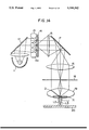
- FIG. 14 is a view showing the optical system of a projection aligner in accordance with a seventh embodiment
- FIG. 15 is a plan view showing a pupillary member used in the seventh embodiment.
- FIG. 16 is a cross-sectional view of the pupillary member shown in FIG. 15;
- FIG. 17 is a view showing the distribution of the intensity of light on the surface of the wafer when the lights is not focused thereon according to the seventh embodiment
- FIG. 18 is a cross-sectional view showing a pupillary member used in an eighth embodiment.
- FIG. 19 is a plan view showing a pupillary member used in a ninth embodiment.
- FIG. 20 is a cross-sectional view of the pupillary member shown in FIG. 19;
- FIG. 21 is a cross-sectional view showing a pupillary member used in tenth embodiment
- FIGS. 22 and 23 are plan views each showing pupillary members used in eleventh and twelfth embodiments.
- FIG. 24 is a view showing the optical system of the conventional projection aligner
- FIG. 25 is a plan view of a pupillary member used in the aligner shown in FIG. 24.
- FIG. 26 is a cross-sectional view of the pupillary member shown in FIG. 25.
- FIG. 1 is a view showing the optical system of a projection aligner in accordance with a first embodiment of the invention.
- a fly-eye lens 13 is disposed diagonally to a lamp house 11 from which a lamp emits light having a wavelength of ⁇ , and a mirror 12 is disposed between the lens 13 and the house 11.
- An aperture member 14 is positioned in front of the fly-eye lens 13.
- Condenser lenses 15 and 16, a mirror 17, and an exposure mask 18 on which a desired circuit pattern is formed are arranged along an optical path.
- a wafer 20 is situated in front of the mask 18, and a projecting lens system 19 is disposed between the mask 18 and the wafer 20.
- a pupillary member 21 is disposed on a pupillary surface of the projecting lens system 19.
- the pupillary member 21 has a disk-like outer frame 22 and an annular phase shift member 23 having a width W.
- a circular opening 22a having a radius A is formed at the center of the frame 22.
- the phase shift member 23 is formed around the periphery of the opening 22a.
- the outer frame 22 is formed of a light-intercepting, i.e., opaque member such as metal.
- the opening 22a forms a transmitting zone D through which light from the lamp house 11 is transmitted.
- the phase shift member 23 is formed of, for example, SiO 2 , and is also formed to such a thickness that there is a phase difference of a half-wavelength, ⁇ /2, between light transmitted through the center of the transmitting zone D, where there is no phase shift member 23 present, and light transmitted through the phase shift member 23.
- the phases of light beams L2 and L3 transmitted through the phase shift member 23 of the pupillary member 21 are reversed with respect to the phase of light beam L1 transmitted through the center of the transmitting zone D. Therefore, when these light beams L1-L3 collect on the surface of the wafer 20, the light beams L2 and L3 each in a reverse phase interfere with the light beam L1, thus offsetting each other.
- FIG. 4 is a view showing the distribution of the intensity of light on the surface of the wafer when the light beams are completely focused thereon. If the pupillary member 21 were not provided with the phase shift member 23, the distribution would be formed as indicated by a broken line 25. In this embodiment, however, because the pupillary member 21 is provided with the phase shift member 23, the light beam L1 is offset by a reverse component 26 of the light beams L2 and L3, and thus the distribution of the intensity of light is formed as indicated by a solid line 24. It is thus proved that when the lights are completely focused, because of the provision of the phase shift member 23, there is a decrease in the intensity of light, but there is substantially no deterioration in the shape of the distribution of the intensity of light.
- the light beams L1-L3 do not converge at one point on the surface of the wafer 20.
- the reverse components of light beams L2 and L3, transmitted through the phase shift member 23 are distributed only around the center of a portion where the light beam L1 is most intense. For this reason, only the intensity of light around a distribution line formed when the pupillary member 21 is not provided with the phase shift member 23 is offset by reverse components 29 and 30 of the light beams L2 and L3. In reality, the intensity of light is distributed as indicated by a solid line 27.
- the projection aligner shown in FIG. 1 permits enlargement of the DOF, as described above, while at the same time increasing the numerical aperture NA.
- FIG. 7 shows the results of the simulation.
- the abscissa of FIG. 7 indicates the degree of focus, the amount of defocus increasing toward the right.
- the ordinate indicates the width of a 25% distribution of the maximum intensity Ip, that is, one/fourth of the Ip of the optical image, as shown in FIG. 4.
- Symbol B O in FIG. 7 indicates an example of an allowable value of the width of the optical image when the circuit pattern is transcribed. An optical image having a width B not greater than the allowable value B O is required for accurate transcription.
- the phase difference between light transmitted through the center of the transmitting zone D and light transmitted through a portion around the transmitting zone D, due to the phase shift member 23, is not limited to a half-wavelength.
- the use of the half-wavelength is the most effective in enlarging the DOF.
- FIG. 8 shows a pupillary member 41 used in a second embodiment.
- the pupillary member 41 is constructed in such a way that an outer frame 42, and a phase shift member 43 are formed on the some crystalling substrate 44.
- the deposition of SiO 2 on the crystal substrate 44 permits easy formation of the phase shift member 43.
- FIGS. 9 and 10 both show a pupillary member 51 used in a third embodiment.
- the pupillary member 51 is constructed in such a manner that a circular phase shift member 53 is formed at the center of a circular opening 52a in an outer frame. 52.
- the phase shift member 53 is formed on a crystalling substrate 54.
- the phase of light transmitted through the center of a transmitting zone D is reversed with respect to the phase of light transmitted through a portion around the zone D.
- the same advantage as that described with the pupillary member 21 is obtainable.
- FIG. 11 shows a pupillary member 61 used in a fourth embodiment.
- the pupillary member 61 is constructed in the following way. First, an outer frame 62 and a phase shift member 63 are formed on a crystalling substrate 64. Then, antireflection films 65 and 66 made of, for example, MgF 2 , are formed on the phase shift member 63 and the crystalling substrate 64 exposed outside. The formation of the antireflection films 65 and 66 reduces the amount of stray light, thus resulting in improved resolution and contrast of an image.
- the antireflection film may be formed on either the obverse or the reverse surface of a transmitting zone D.
- the antireflection films are formed on the pupillary member with the structure shown in FIG. 8, they may be provided on any of the pupillary members with the structures described above. The same advantage as that described above is obtainable.
- FIGS. 12 and 13 each show pupillary members used in fifth and sixth embodiments. If the circuit pattern formed on the mask 18 is a minute pattern, first order diffraction of light by this pattern has a great effect. That is, if it is a rectangular pattern, pattern images made by the first order diffracted light are formed around a pattern image made by zero order diffracted light; and if it is a line-and-space pattern, pattern images made by the first order diffracted light are formed on both sides of the pattern image made by the zero order diffracted light.
- a pupillary member 111 may be employed. At the center of the member 111 a first transmitting zone D 1 for the zero order diffracted light is formed. Second transmitting zones D 2 for the first order diffraction of light are formed around the first transmitting zone D 1 .
- a pupillary member 112 may be employed, at the center of which member 112 a first transmitting zone D 1 for the zero order diffracted light is formed. Second transmitting zones D 2 for the first order diffracted light are formed on both sides of the first transmitting zone D 1 .
- the respective transmitting zones D 1 and D 2 of the pupillary members 111 and 112 have structures similar to those of the pupillary members shown in FIGS. 2 and 3, and 8 to 11.
- pupillary members 111 and 112 can reduce the intensity of light around the first order diffracted light of the circuit pattern, thus improving image contrast.
- FIG. 14 is a view showing the optical system of a projection aligner in accordance with a seventh embodiment of this invention.
- a pupillary member 71 is used in place of the pupillary member 21 of the optical system in the first embodiment shown in FIG. 1.
- the pupillary member 71 has a circular outer frame 72, an annular, phase shift member 73, and an annular light-intercepting i.e., opaque member 74.
- a circular opening 72a having a radius A is formed at the center of the outer frame 72.
- the phase shift member 73 having a width W 1 is formed around the periphery of the opening 72a.
- the light-intercepting member 74 having a width W 2 is formed around the inside periphery of the phase shift member 73. In other words, the center of a transmitting zone D is separated by the light-intercepting member 74 from a portion around the zone D.
- the outer frame 72 and the light-intercepting member 74 are made of a material, such as metal, which blocks light.
- the phase shift member 73 is made of, for instance, SiO 2 .
- the pupillary member 71 having a such a light-intercepting member 74 When the pupillary member 71 having a such a light-intercepting member 74 is used, as indicated by dot chain lines of FIG. 17 when the light beams are not focused, the centers of reverse components 36 and 37 of light beams L2 and L3, transmitted through the phase shift member 73, will deviate in an amount equal to a predetermined distance W 3 from components 38 of a light beam L1 which are positioned most outwardly. For this reason, only light in a portion around a distribution line formed when the pupillary member 71 is not provided with the phase shift member 73 is offset by the reverse components 36 and 37 of the light beams L2 and L3. In reality, the intensity of light is distributed as indicated by a solid line 34.
- the ratio W 2 /A of the width W 2 of the light-intercepting member 74 to the radius A of the transmitting zone D of the pupillary member 71 was changed and a circular contact hole pattern was exposed. It was found that when the ratio W 2 /A is about 3%, the circuit pattern can be most stably transcribed.
- a pupillary member 81 constructed in such a way that an outer frame 82, a phase shift member 83, and a light-intercepting member 84 are formed on the same crystalling substrate 85.
- the deposition of SiO 2 and metal on the crystalling substrate 85 permits easy formation of the phase shift member 83 and the light-intercepting member 84.
- a circular phase shift member 93 may be formed at the center of a circular opening 92a in an outer frame 92 and a light-intercepting member 94 may be formed around the phase shift member 93.
- the phase shift member 93 and the light-intercepting member 94 are formed on a crystalling substrate 95.
- the formation of antireflection films 106 and 107 made of, for example, MgF 2 reduces the amount of stray light, thus resulting in improved resolution and contrast of an image.
- an outer frame 102, a phase shift member 103, and a light-intercepting member 104 are formed on a crystalling substrate 105.
- the antireflection film 106 is formed on the phase shift member 103, the light-intercepting member 104 and the obverse side of the crystalling substrate 105, and the antireflection film 107 is formed on the reverse side of the crystalling substrate 105.
- the antireflection film may be formed on either the obverse or the reverse surface of a transmitting zone D.
- the antireflection films are formed on the pupillary member with the structure shown in FIG. 18, they may be provided on a pupillary member with a different structure. The same advantage as that described above is obtainable.
- the use of a pupillary member 113 effectively improves image contrast when the minute rectangular pattern is formed on the mask 18.
- the pupillary member 113 has a primary transmitting zone D 1 for the zero order diffracted light, and four secondary transmitting zones D 2 for the first order diffracted light.
- a light-intercepting member 113a for separating the center of each zone from a portion around this center is formed in each of the transmitting zones D 1 and D 2 .
- the use of a pupillary member 114 effectively improves image contrast when the minute line-and-space pattern is formed on the mask 18.
- the pupillary member 114 has a primary transmitting zone D 1 for the zero order diffracted light, and two secondary transmitting zones D 2 for the first order diffracted light.
- a light-intercepting member 114a for separating the center of each zone from a portion around this center is formed in each of the transmitting zones D 1 and D 2 .
- the respective transmitting zones D 1 and D.sub. 2 of the pupillary members 113 and 114 have structures similar to those of the pupillary members shown in FIGS. 15 and 16, and 18 to 21.
Abstract
Description
Claims (17)
Applications Claiming Priority (4)
| Application Number | Priority Date | Filing Date | Title |
|---|---|---|---|
| JP2306238A JP2587133B2 (en) | 1990-11-14 | 1990-11-14 | Projection exposure apparatus and semiconductor device exposed and manufactured by the apparatus |
| JP2-306238 | 1990-11-14 | ||
| JP3011541A JP2581846B2 (en) | 1991-01-08 | 1991-01-08 | Projection exposure equipment |
| JP3-11541 | 1991-01-08 |
Publications (1)
| Publication Number | Publication Date |
|---|---|
| US5144362A true US5144362A (en) | 1992-09-01 |
Family
ID=26346980
Family Applications (1)
| Application Number | Title | Priority Date | Filing Date |
|---|---|---|---|
| US07/790,446 Expired - Lifetime US5144362A (en) | 1990-11-14 | 1991-11-12 | Projection aligner |
Country Status (1)
| Country | Link |
|---|---|
| US (1) | US5144362A (en) |
Cited By (49)
| Publication number | Priority date | Publication date | Assignee | Title |
|---|---|---|---|---|
| US5208629A (en) * | 1991-04-05 | 1993-05-04 | Nippon Telegraph & Telephone Corporation | Optical projection exposure method and system using the same |
| US5264898A (en) * | 1991-08-29 | 1993-11-23 | Mitsubishi Denki Kabushiki Kaisha | Projection exposure apparatus |
| US5272501A (en) * | 1991-08-28 | 1993-12-21 | Nikon Corporation | Projection exposure apparatus |
| US5274420A (en) * | 1992-04-20 | 1993-12-28 | International Business Machines Corporation | Beamsplitter type lens elements with pupil-plane stops for lithographic systems |
| US5287142A (en) * | 1991-12-10 | 1994-02-15 | Mitsubishi Denki Kabushiki Kaisha | Projection exposure apparatus |
| US5296892A (en) * | 1992-02-01 | 1994-03-22 | Nikon Corporation | Illuminating apparatus and projection exposure apparatus provided with such an illuminating apparatus |
| US5300967A (en) * | 1992-07-31 | 1994-04-05 | Mitsubishi Denki Kabushiki Kaisha | Projection exposure apparatus |
| US5302999A (en) * | 1992-02-04 | 1994-04-12 | Hitachi, Ltd. | Illumination method, illumination apparatus and projection exposure apparatus |
| US5305054A (en) * | 1991-02-22 | 1994-04-19 | Canon Kabushiki Kaisha | Imaging method for manufacture of microdevices |
| US5311249A (en) * | 1992-02-13 | 1994-05-10 | Mitsubishi Denki Kabushiki Kaisha | Projection exposure apparatus |
| US5317450A (en) * | 1991-12-17 | 1994-05-31 | Mitsubishi Denki Kabushiki Kaisha | Projection exposure apparatus |
| US5323208A (en) * | 1992-03-09 | 1994-06-21 | Hitachi, Ltd. | Projection exposure apparatus |
| US5329335A (en) * | 1992-03-17 | 1994-07-12 | Nippon Steel Corporation | Method and apparatus for projection exposure |
| US5331369A (en) * | 1991-09-20 | 1994-07-19 | Hitachi, Ltd. | Method of forming patterns and apparatus for carrying out the same |
| US5335044A (en) * | 1992-02-26 | 1994-08-02 | Nikon Corporation | Projection type exposure apparatus and method of exposure |
| US5345292A (en) * | 1992-03-31 | 1994-09-06 | Canon Kabushiki Kaisha | Illumination device for projection exposure apparatus |
| US5357311A (en) * | 1991-02-25 | 1994-10-18 | Nikon Corporation | Projection type light exposure apparatus and light exposure method |
| US5367358A (en) * | 1992-10-09 | 1994-11-22 | Mitsubishi Denki Kabushiki Kaisha | Projection exposing apparatus and projection exposing method |
| EP0638847A1 (en) * | 1993-07-15 | 1995-02-15 | Nikon Corporation | Apparatus and method for projection exposure |
| US5396311A (en) * | 1992-09-18 | 1995-03-07 | Sharp Kabushiki Kaisha | Filter for projection photolithographic system |
| US5405721A (en) * | 1992-08-18 | 1995-04-11 | At&T Corp. | Phase-shifting lithographic masks having phase-shifting layers of differing compositions |
| US5424803A (en) * | 1991-08-09 | 1995-06-13 | Canon Kabushiki Kaisha | Projection exposure apparatus and semiconductor device manufacturing method |
| US5432588A (en) * | 1993-02-08 | 1995-07-11 | Mitsubishi Denk Kabushiki Kaisha | Semiconductor device and method of making the semiconductor device |
| US5434647A (en) * | 1993-05-14 | 1995-07-18 | Nec Corporation | Projector for exposing photosensitive substrate |
| US5436114A (en) * | 1989-12-06 | 1995-07-25 | Hitachi, Ltd. | Method of optical lithography with super resolution and projection printing apparatus |
| EP0720055A1 (en) * | 1994-12-28 | 1996-07-03 | International Business Machines Corporation | Focal plane phase-shifting lithography |
| US5552856A (en) * | 1993-06-14 | 1996-09-03 | Nikon Corporation | Projection exposure apparatus |
| US5574492A (en) * | 1992-03-27 | 1996-11-12 | Canon Kabushiki Kaisha | Imaging method and semiconductor device manufacturing method using the same |
| US5621500A (en) * | 1995-05-25 | 1997-04-15 | Nikon Corporation | Method and apparatus for projection exposure |
| US5631773A (en) * | 1991-08-02 | 1997-05-20 | Canon Kabushiki Kaisha | Image projection method and semiconductor device manufacturing method using the same |
| US5673102A (en) * | 1991-02-22 | 1997-09-30 | Canon Kabushiki Kaisha | Image farming and microdevice manufacturing method and exposure apparatus in which a light source includes four quadrants of predetermined intensity |
| US5684569A (en) * | 1993-12-22 | 1997-11-04 | Nikon Corporation | Position detecting apparatus and projection exposure apparatus |
| US5715040A (en) * | 1995-10-12 | 1998-02-03 | Kabushiki Kaisha Toshiba | Illumination aperture of low intensity loss |
| US5815247A (en) * | 1995-09-21 | 1998-09-29 | Siemens Aktiengesellschaft | Avoidance of pattern shortening by using off axis illumination with dipole and polarizing apertures |
| US6151103A (en) * | 1996-05-08 | 2000-11-21 | Texas Instruments Incorporated | Method and system for improved optical imaging in microlithography |
| US6212009B1 (en) * | 1997-09-29 | 2001-04-03 | Leica Microsystems Wetzlar Gmbh | Phase annulus to carry out a positive phase contrast |
| US6245470B1 (en) * | 1995-12-14 | 2001-06-12 | Mitsubishi Denki Kabushiki Kaisha | Projection aligner, aberration estimating mask pattern, aberration quantity estimating method, aberration eliminating filter and semiconductor manufacturing method |
| US6310679B1 (en) | 1992-10-01 | 2001-10-30 | Nikon Corporation | Projection exposure method and apparatus |
| US20030117605A1 (en) * | 2001-12-20 | 2003-06-26 | Nanya Technology Corporation | Apparatus and method for contact hole exposure |
| US20030215616A1 (en) * | 2002-05-15 | 2003-11-20 | Numerical Technologies, Inc. | Facilitating optical proximity effect correction through pupil filtering |
| US20040180294A1 (en) * | 2003-02-21 | 2004-09-16 | Asml Holding N.V. | Lithographic printing with polarized light |
| US20050146701A1 (en) * | 2002-04-29 | 2005-07-07 | Carl Zeiss Smt Ag | Projection method including pupillary filtering and a projection lens therefor |
| DE102004011733A1 (en) * | 2004-03-04 | 2005-09-22 | Carl Zeiss Smt Ag | Transmission filter apparatus |
| US20060092398A1 (en) * | 2004-11-02 | 2006-05-04 | Asml Holding N.V. | Method and apparatus for variable polarization control in a lithography system |
| US20060197933A1 (en) * | 2005-03-03 | 2006-09-07 | Canon Kabushiki Kaisha | Exposure apparatus |
| US20070121090A1 (en) * | 2005-11-30 | 2007-05-31 | Asml Netherlands B.V. | Lithographic apparatus and device manufacturing method |
| US20100123887A1 (en) * | 2008-11-17 | 2010-05-20 | Asml Netherlands B.V. | Method for a lithographic apparatus |
| US8027091B2 (en) | 2006-05-18 | 2011-09-27 | Carl Zeiss Smt Gmbh | Method for correcting optical proximity effects |
| US20120092637A1 (en) * | 2007-09-18 | 2012-04-19 | Carl Zeiss Smt Gmbh | Microlithographic projection exposure apparatus |
Citations (6)
| Publication number | Priority date | Publication date | Assignee | Title |
|---|---|---|---|---|
| US3157087A (en) * | 1961-12-26 | 1964-11-17 | Pako Corp | Optical light distribution system for a photographic projection printer |
| US3892482A (en) * | 1974-03-07 | 1975-07-01 | Berkey Photo Inc | Color correcting illumination system for color enlargers and the like |
| US4257086A (en) * | 1979-10-22 | 1981-03-17 | Koehler Manufacturing Company | Method and apparatus for controlling radiant energy |
| US4816876A (en) * | 1985-11-27 | 1989-03-28 | Pryor Paul L | Contrast control for lens |
| US4970546A (en) * | 1988-04-07 | 1990-11-13 | Nikon Corporation | Exposure control device |
| US4988188A (en) * | 1987-08-31 | 1991-01-29 | Canon Kabushiki Kaisha | Illumination device |
-
1991
- 1991-11-12 US US07/790,446 patent/US5144362A/en not_active Expired - Lifetime
Patent Citations (6)
| Publication number | Priority date | Publication date | Assignee | Title |
|---|---|---|---|---|
| US3157087A (en) * | 1961-12-26 | 1964-11-17 | Pako Corp | Optical light distribution system for a photographic projection printer |
| US3892482A (en) * | 1974-03-07 | 1975-07-01 | Berkey Photo Inc | Color correcting illumination system for color enlargers and the like |
| US4257086A (en) * | 1979-10-22 | 1981-03-17 | Koehler Manufacturing Company | Method and apparatus for controlling radiant energy |
| US4816876A (en) * | 1985-11-27 | 1989-03-28 | Pryor Paul L | Contrast control for lens |
| US4988188A (en) * | 1987-08-31 | 1991-01-29 | Canon Kabushiki Kaisha | Illumination device |
| US4970546A (en) * | 1988-04-07 | 1990-11-13 | Nikon Corporation | Exposure control device |
Cited By (78)
| Publication number | Priority date | Publication date | Assignee | Title |
|---|---|---|---|---|
| US5436114A (en) * | 1989-12-06 | 1995-07-25 | Hitachi, Ltd. | Method of optical lithography with super resolution and projection printing apparatus |
| US6271909B1 (en) | 1991-02-22 | 2001-08-07 | Canon Kabushiki Kaisha | Exposure apparatus and device manufacturing method including changing a photo-intensity distribution of a light source and adjusting an illuminance distribution on a substrate in accordance with the change |
| US6473160B2 (en) | 1991-02-22 | 2002-10-29 | Canon Kabushiki Kaisha | Projection exposure apparatus and device manufacturing method including an aperture member having a circular light transmitting portion and a light blocking member |
| US6128068A (en) * | 1991-02-22 | 2000-10-03 | Canon Kabushiki Kaisha | Projection exposure apparatus including an illumination optical system that forms a secondary light source with a particular intensity distribution |
| US20040080736A1 (en) * | 1991-02-22 | 2004-04-29 | Canon Kabushiki Kaisha | Imaging method for manufacture of microdevices |
| US6654101B2 (en) | 1991-02-22 | 2003-11-25 | Canon Kabushiki Kaisha | Exposure apparatus and device manufacturing method including changing a photo-intensity distribution of a light source and adjusting an illuminance distribution on a substrate in accordance with the change |
| US6084655A (en) * | 1991-02-22 | 2000-07-04 | Canon Kabushiki Kaisha | Imaging method for manufacture of microdevices |
| US5673102A (en) * | 1991-02-22 | 1997-09-30 | Canon Kabushiki Kaisha | Image farming and microdevice manufacturing method and exposure apparatus in which a light source includes four quadrants of predetermined intensity |
| US5305054A (en) * | 1991-02-22 | 1994-04-19 | Canon Kabushiki Kaisha | Imaging method for manufacture of microdevices |
| US5357311A (en) * | 1991-02-25 | 1994-10-18 | Nikon Corporation | Projection type light exposure apparatus and light exposure method |
| US5208629A (en) * | 1991-04-05 | 1993-05-04 | Nippon Telegraph & Telephone Corporation | Optical projection exposure method and system using the same |
| US5631773A (en) * | 1991-08-02 | 1997-05-20 | Canon Kabushiki Kaisha | Image projection method and semiconductor device manufacturing method using the same |
| US5424803A (en) * | 1991-08-09 | 1995-06-13 | Canon Kabushiki Kaisha | Projection exposure apparatus and semiconductor device manufacturing method |
| US5272501A (en) * | 1991-08-28 | 1993-12-21 | Nikon Corporation | Projection exposure apparatus |
| US5264898A (en) * | 1991-08-29 | 1993-11-23 | Mitsubishi Denki Kabushiki Kaisha | Projection exposure apparatus |
| US5331369A (en) * | 1991-09-20 | 1994-07-19 | Hitachi, Ltd. | Method of forming patterns and apparatus for carrying out the same |
| US5287142A (en) * | 1991-12-10 | 1994-02-15 | Mitsubishi Denki Kabushiki Kaisha | Projection exposure apparatus |
| US5317450A (en) * | 1991-12-17 | 1994-05-31 | Mitsubishi Denki Kabushiki Kaisha | Projection exposure apparatus |
| US5296892A (en) * | 1992-02-01 | 1994-03-22 | Nikon Corporation | Illuminating apparatus and projection exposure apparatus provided with such an illuminating apparatus |
| US5302999A (en) * | 1992-02-04 | 1994-04-12 | Hitachi, Ltd. | Illumination method, illumination apparatus and projection exposure apparatus |
| US5311249A (en) * | 1992-02-13 | 1994-05-10 | Mitsubishi Denki Kabushiki Kaisha | Projection exposure apparatus |
| US5335044A (en) * | 1992-02-26 | 1994-08-02 | Nikon Corporation | Projection type exposure apparatus and method of exposure |
| US5323208A (en) * | 1992-03-09 | 1994-06-21 | Hitachi, Ltd. | Projection exposure apparatus |
| US5329335A (en) * | 1992-03-17 | 1994-07-12 | Nippon Steel Corporation | Method and apparatus for projection exposure |
| US5574492A (en) * | 1992-03-27 | 1996-11-12 | Canon Kabushiki Kaisha | Imaging method and semiconductor device manufacturing method using the same |
| US5345292A (en) * | 1992-03-31 | 1994-09-06 | Canon Kabushiki Kaisha | Illumination device for projection exposure apparatus |
| US5726740A (en) * | 1992-03-31 | 1998-03-10 | Canon Kabushiki Kaisha | Projection exposure apparatus having illumination device with ring-like or spot-like light source |
| US5274420A (en) * | 1992-04-20 | 1993-12-28 | International Business Machines Corporation | Beamsplitter type lens elements with pupil-plane stops for lithographic systems |
| US5300967A (en) * | 1992-07-31 | 1994-04-05 | Mitsubishi Denki Kabushiki Kaisha | Projection exposure apparatus |
| US5405721A (en) * | 1992-08-18 | 1995-04-11 | At&T Corp. | Phase-shifting lithographic masks having phase-shifting layers of differing compositions |
| US5396311A (en) * | 1992-09-18 | 1995-03-07 | Sharp Kabushiki Kaisha | Filter for projection photolithographic system |
| US6404482B1 (en) | 1992-10-01 | 2002-06-11 | Nikon Corporation | Projection exposure method and apparatus |
| US6310679B1 (en) | 1992-10-01 | 2001-10-30 | Nikon Corporation | Projection exposure method and apparatus |
| US5367358A (en) * | 1992-10-09 | 1994-11-22 | Mitsubishi Denki Kabushiki Kaisha | Projection exposing apparatus and projection exposing method |
| US5432588A (en) * | 1993-02-08 | 1995-07-11 | Mitsubishi Denk Kabushiki Kaisha | Semiconductor device and method of making the semiconductor device |
| US5434647A (en) * | 1993-05-14 | 1995-07-18 | Nec Corporation | Projector for exposing photosensitive substrate |
| US5552856A (en) * | 1993-06-14 | 1996-09-03 | Nikon Corporation | Projection exposure apparatus |
| EP0638847A1 (en) * | 1993-07-15 | 1995-02-15 | Nikon Corporation | Apparatus and method for projection exposure |
| EP0834771A1 (en) * | 1993-07-15 | 1998-04-08 | Nikon Corporation | Apparatus and method for projection exposure |
| US5684569A (en) * | 1993-12-22 | 1997-11-04 | Nikon Corporation | Position detecting apparatus and projection exposure apparatus |
| EP0720055A1 (en) * | 1994-12-28 | 1996-07-03 | International Business Machines Corporation | Focal plane phase-shifting lithography |
| US5650632A (en) * | 1994-12-28 | 1997-07-22 | International Business Machines Corporation | Focal plane phase-shifting lithography |
| US5621500A (en) * | 1995-05-25 | 1997-04-15 | Nikon Corporation | Method and apparatus for projection exposure |
| US5815247A (en) * | 1995-09-21 | 1998-09-29 | Siemens Aktiengesellschaft | Avoidance of pattern shortening by using off axis illumination with dipole and polarizing apertures |
| US5715040A (en) * | 1995-10-12 | 1998-02-03 | Kabushiki Kaisha Toshiba | Illumination aperture of low intensity loss |
| US6245470B1 (en) * | 1995-12-14 | 2001-06-12 | Mitsubishi Denki Kabushiki Kaisha | Projection aligner, aberration estimating mask pattern, aberration quantity estimating method, aberration eliminating filter and semiconductor manufacturing method |
| US6517983B2 (en) | 1995-12-14 | 2003-02-11 | Mitsubishi Denki Kabushiki Kaisha | Aberration estimating mask pattern |
| US20030123038A1 (en) * | 1995-12-14 | 2003-07-03 | Mitsubishi Denki Kabushiki Kaisha | Projection aligner, aberration estimating mask pattern,aberration quantity estimating method, aberration eliminating filter and semiconductor manufacturing method |
| US6970291B2 (en) | 1995-12-14 | 2005-11-29 | Mitsubishi Denki Kabushiki Kaisha | Projection aligner, aberration estimating mask pattern, aberration quantity estimating method, aberration eliminating filter and semiconductor manufacturing method |
| US7170682B2 (en) | 1995-12-14 | 2007-01-30 | Renesas Technology Corp. | Projection aligner, aberration estimating mask pattern, aberration quantity estimating method, aberration eliminating filter and semiconductor manufacturing method |
| US6151103A (en) * | 1996-05-08 | 2000-11-21 | Texas Instruments Incorporated | Method and system for improved optical imaging in microlithography |
| US6212009B1 (en) * | 1997-09-29 | 2001-04-03 | Leica Microsystems Wetzlar Gmbh | Phase annulus to carry out a positive phase contrast |
| US20030117605A1 (en) * | 2001-12-20 | 2003-06-26 | Nanya Technology Corporation | Apparatus and method for contact hole exposure |
| US7791711B2 (en) | 2002-04-29 | 2010-09-07 | Carl Zeiss Smt Ag | Projection method including pupillary filtering and a projection lens therefor |
| US7336342B2 (en) | 2002-04-29 | 2008-02-26 | Carl Zeiss Smt Ag | Projection method including pupillary filtering and a projection lens therefor |
| US20050146701A1 (en) * | 2002-04-29 | 2005-07-07 | Carl Zeiss Smt Ag | Projection method including pupillary filtering and a projection lens therefor |
| US6846617B2 (en) | 2002-05-15 | 2005-01-25 | Numerical Technologies | Facilitating optical proximity effect correction through pupil filtering |
| US20030215616A1 (en) * | 2002-05-15 | 2003-11-20 | Numerical Technologies, Inc. | Facilitating optical proximity effect correction through pupil filtering |
| US20040180294A1 (en) * | 2003-02-21 | 2004-09-16 | Asml Holding N.V. | Lithographic printing with polarized light |
| US7090964B2 (en) | 2003-02-21 | 2006-08-15 | Asml Holding N.V. | Lithographic printing with polarized light |
| US7445883B2 (en) | 2003-02-21 | 2008-11-04 | Asml Holding N.V. | Lithographic printing with polarized light |
| US7940375B2 (en) | 2004-03-04 | 2011-05-10 | Carl Zeiss Smt Gmbh | Transmission filter apparatus |
| DE102004011733A1 (en) * | 2004-03-04 | 2005-09-22 | Carl Zeiss Smt Ag | Transmission filter apparatus |
| US20070279613A1 (en) * | 2004-03-04 | 2007-12-06 | Carl Zeiss Smt Ag | Transmission Filter Apparatus |
| US8049866B2 (en) | 2004-11-02 | 2011-11-01 | Asml Holding N.V. | Method and apparatus for variable polarization control in a lithography system |
| US20060092398A1 (en) * | 2004-11-02 | 2006-05-04 | Asml Holding N.V. | Method and apparatus for variable polarization control in a lithography system |
| US7271874B2 (en) | 2004-11-02 | 2007-09-18 | Asml Holding N.V. | Method and apparatus for variable polarization control in a lithography system |
| US20070291248A1 (en) * | 2004-11-02 | 2007-12-20 | Asml Holding N.V. | Method and apparatus for variable polarization control in a lithography system |
| US7518707B2 (en) * | 2005-03-03 | 2009-04-14 | Canon Kabushiki Kaisha | Exposure apparatus |
| US20060197933A1 (en) * | 2005-03-03 | 2006-09-07 | Canon Kabushiki Kaisha | Exposure apparatus |
| US20070121090A1 (en) * | 2005-11-30 | 2007-05-31 | Asml Netherlands B.V. | Lithographic apparatus and device manufacturing method |
| US8405907B2 (en) | 2006-05-18 | 2013-03-26 | Carl Zeiss Smt Gmbh | Method for correcting optical proximity effects |
| US8027091B2 (en) | 2006-05-18 | 2011-09-27 | Carl Zeiss Smt Gmbh | Method for correcting optical proximity effects |
| US20120092637A1 (en) * | 2007-09-18 | 2012-04-19 | Carl Zeiss Smt Gmbh | Microlithographic projection exposure apparatus |
| US8982325B2 (en) * | 2007-09-18 | 2015-03-17 | Carl Zeiss Smt Gmbh | Microlithographic projection exposure apparatus |
| US20100123887A1 (en) * | 2008-11-17 | 2010-05-20 | Asml Netherlands B.V. | Method for a lithographic apparatus |
| US9535341B2 (en) | 2008-11-17 | 2017-01-03 | Asml Netherlands B.V. | Method for a lithographic apparatus |
| US10331042B2 (en) | 2008-11-17 | 2019-06-25 | Asml Netherlands B.V. | Method for a lithographic apparatus |
Similar Documents
| Publication | Publication Date | Title |
|---|---|---|
| US5144362A (en) | Projection aligner | |
| US5253040A (en) | Projection aligner | |
| US5264898A (en) | Projection exposure apparatus | |
| US5499137A (en) | Exposure method and apparatus therefor | |
| EP0638847B1 (en) | Apparatus and method for projection exposure | |
| US6004699A (en) | Photomask used for projection exposure with phase shifted auxiliary pattern | |
| US7629087B2 (en) | Photomask, method of making a photomask and photolithography method and system using the same | |
| US6890692B2 (en) | Method of focus monitoring and manufacturing method for an electronic device | |
| KR0153221B1 (en) | Spatial filter used for reduction type projection printing apparatus | |
| US5698347A (en) | Reticle for off-axis illumination | |
| JP3287017B2 (en) | Measurement method of imaging characteristics | |
| US5393623A (en) | Exposure apparatus employing a photomask | |
| US5311249A (en) | Projection exposure apparatus | |
| JPH06163350A (en) | Projection exposure method and device thereof | |
| JPH10233361A (en) | Exposure and exposure mask | |
| JP2972528B2 (en) | Exposure method | |
| US5432588A (en) | Semiconductor device and method of making the semiconductor device | |
| JPH05281698A (en) | Photomask and pattern transfer method | |
| JPH08181065A (en) | Pattern forming method, manufacture of semiconductor device using thereof | |
| US5434647A (en) | Projector for exposing photosensitive substrate | |
| JPH05315226A (en) | Projection aligner | |
| JP2908100B2 (en) | Projection exposure apparatus and method of manufacturing semiconductor device | |
| JP2581845B2 (en) | Projection exposure equipment | |
| KR0183706B1 (en) | Projection exposure method, the mask thereof | |
| JP2581846B2 (en) | Projection exposure equipment |
Legal Events
| Date | Code | Title | Description |
|---|---|---|---|
| AS | Assignment |
Owner name: MITSUBISHI DENKI KABUSHIKI KAISHA Free format text: ASSIGNMENT OF ASSIGNORS INTEREST.;ASSIGNORS:KAMON, KAZUYA;MYOI, YASUHITO;MIYAMOTO, TERUO;AND OTHERS;REEL/FRAME:005958/0699;SIGNING DATES FROM 19911107 TO 19911111 |
|
| STCF | Information on status: patent grant |
Free format text: PATENTED CASE |
|
| FEPP | Fee payment procedure |
Free format text: PAYOR NUMBER ASSIGNED (ORIGINAL EVENT CODE: ASPN); ENTITY STATUS OF PATENT OWNER: LARGE ENTITY |
|
| FPAY | Fee payment |
Year of fee payment: 4 |
|
| FPAY | Fee payment |
Year of fee payment: 8 |
|
| FPAY | Fee payment |
Year of fee payment: 12 |
|
| AS | Assignment |
Owner name: RENESAS ELECTRONICS CORPORATION, JAPAN Free format text: ASSIGNMENT OF ASSIGNORS INTEREST;ASSIGNOR:MITSUBISHI DENKI KABUSHIKI KAISHA;REEL/FRAME:025980/0219 Effective date: 20110307 |