US5124776A - Bipolar integrated circuit having a unit block structure - Google Patents
Bipolar integrated circuit having a unit block structure Download PDFInfo
- Publication number
- US5124776A US5124776A US07/492,898 US49289890A US5124776A US 5124776 A US5124776 A US 5124776A US 49289890 A US49289890 A US 49289890A US 5124776 A US5124776 A US 5124776A
- Authority
- US
- United States
- Prior art keywords
- power
- integrated circuit
- feed system
- power feed
- hierarchical
- Prior art date
- Legal status (The legal status is an assumption and is not a legal conclusion. Google has not performed a legal analysis and makes no representation as to the accuracy of the status listed.)
- Expired - Lifetime
Links
- 239000004065 semiconductor Substances 0.000 claims abstract description 45
- 239000004020 conductor Substances 0.000 claims description 137
- 238000000926 separation method Methods 0.000 claims 1
- 230000010354 integration Effects 0.000 description 15
- 238000000034 method Methods 0.000 description 15
- 230000008569 process Effects 0.000 description 11
- 238000010276 construction Methods 0.000 description 10
- 238000011960 computer-aided design Methods 0.000 description 9
- 238000013461 design Methods 0.000 description 7
- 230000007423 decrease Effects 0.000 description 6
- 238000010586 diagram Methods 0.000 description 5
- 230000006870 function Effects 0.000 description 5
- 238000004088 simulation Methods 0.000 description 5
- 230000003247 decreasing effect Effects 0.000 description 4
- 230000015654 memory Effects 0.000 description 4
- 230000004048 modification Effects 0.000 description 4
- 238000012986 modification Methods 0.000 description 4
- 239000010410 layer Substances 0.000 description 3
- 238000004519 manufacturing process Methods 0.000 description 2
- 230000002776 aggregation Effects 0.000 description 1
- 238000004220 aggregation Methods 0.000 description 1
- 238000009411 base construction Methods 0.000 description 1
- 238000005056 compaction Methods 0.000 description 1
- 238000012937 correction Methods 0.000 description 1
- 239000012212 insulator Substances 0.000 description 1
- 239000011229 interlayer Substances 0.000 description 1
- 230000009467 reduction Effects 0.000 description 1
Images


Classifications
-
- H—ELECTRICITY
- H01—ELECTRIC ELEMENTS
- H01L—SEMICONDUCTOR DEVICES NOT COVERED BY CLASS H10
- H01L29/00—Semiconductor devices adapted for rectifying, amplifying, oscillating or switching, or capacitors or resistors with at least one potential-jump barrier or surface barrier, e.g. PN junction depletion layer or carrier concentration layer; Details of semiconductor bodies or of electrodes thereof ; Multistep manufacturing processes therefor
- H01L29/66—Types of semiconductor device ; Multistep manufacturing processes therefor
- H01L29/68—Types of semiconductor device ; Multistep manufacturing processes therefor controllable by only the electric current supplied, or only the electric potential applied, to an electrode which does not carry the current to be rectified, amplified or switched
- H01L29/70—Bipolar devices
-
- H—ELECTRICITY
- H01—ELECTRIC ELEMENTS
- H01L—SEMICONDUCTOR DEVICES NOT COVERED BY CLASS H10
- H01L27/00—Devices consisting of a plurality of semiconductor or other solid-state components formed in or on a common substrate
- H01L27/02—Devices consisting of a plurality of semiconductor or other solid-state components formed in or on a common substrate including semiconductor components specially adapted for rectifying, oscillating, amplifying or switching and having at least one potential-jump barrier or surface barrier; including integrated passive circuit elements with at least one potential-jump barrier or surface barrier
- H01L27/04—Devices consisting of a plurality of semiconductor or other solid-state components formed in or on a common substrate including semiconductor components specially adapted for rectifying, oscillating, amplifying or switching and having at least one potential-jump barrier or surface barrier; including integrated passive circuit elements with at least one potential-jump barrier or surface barrier the substrate being a semiconductor body
- H01L27/10—Devices consisting of a plurality of semiconductor or other solid-state components formed in or on a common substrate including semiconductor components specially adapted for rectifying, oscillating, amplifying or switching and having at least one potential-jump barrier or surface barrier; including integrated passive circuit elements with at least one potential-jump barrier or surface barrier the substrate being a semiconductor body including a plurality of individual components in a repetitive configuration
- H01L27/118—Masterslice integrated circuits
- H01L27/11801—Masterslice integrated circuits using bipolar technology
-
- H—ELECTRICITY
- H01—ELECTRIC ELEMENTS
- H01L—SEMICONDUCTOR DEVICES NOT COVERED BY CLASS H10
- H01L21/00—Processes or apparatus adapted for the manufacture or treatment of semiconductor or solid state devices or of parts thereof
- H01L21/70—Manufacture or treatment of devices consisting of a plurality of solid state components formed in or on a common substrate or of parts thereof; Manufacture of integrated circuit devices or of parts thereof
- H01L21/77—Manufacture or treatment of devices consisting of a plurality of solid state components or integrated circuits formed in, or on, a common substrate
- H01L21/78—Manufacture or treatment of devices consisting of a plurality of solid state components or integrated circuits formed in, or on, a common substrate with subsequent division of the substrate into plural individual devices
- H01L21/82—Manufacture or treatment of devices consisting of a plurality of solid state components or integrated circuits formed in, or on, a common substrate with subsequent division of the substrate into plural individual devices to produce devices, e.g. integrated circuits, each consisting of a plurality of components
Definitions
- the present invention generally relates to semiconductor integrated circuits and more particularly to a bipolar integrated circuit having a unit block structure.
- ECL emitter coupled logic
- FIG. 1 a number of logic gates having an identical construction and size are arranged on a surface of a semiconductor chip 10 as an array of basic cells 12.
- the basic cells 12 may be arranged in a plurality of columns 14 or 14a as shown in FIG. 1.
- Each of the cells 12 has an identical size and construction.
- the chip, or master slice, having the structure as shown in FIG. 1, is mass-produced and the interconnection between the basic cells 12 is made according to the specific purpose of the integrated circuit which of course changes depending on the type and function required for the integrated circuit.
- Such an increase in the interconnection invites a decrease in the operational speed of the integrated circuit.
- provision of the interconnection becomes increasingly difficult with increasing integration density because of the appearance of a complicated interconnection pattern on the chip during the process of pattern designing, and finding of a path for new interconnections in the region where interconnections are already provided becomes increasingly difficult.
- a gate array cannot provide a region for memories or other utilities on the chip, as the chip is provided as the master slice wherein the basic cells are provided so as to cover substantially the entire region of the chip.
- each of the logic devices such as inverters, NOR gates, flip-flops and the like are patterned as polycells 16a each having a standardized, constant height when measured in the Y-direction as shown in FIG. 2.
- the polycells further have various widths in the X-direction in the drawing, depending on their types and functions.
- the polycells 16a are assembled in the form of polycell column 16 extending in the X-direction by arranging it so that top edges of adjacent polycells are aligned with each other and bottom edges of adjacent polycells are also aligned with each other as shown in FIG. 2.
- a number of such polycell columns are formed on the chip, and interconnection between the polycells is made either within the cell columns, or using the space between the cell columns, or crossing one or more cell columns.
- this polycell structure By using this polycell structure, one can increase the integration density substantially by optimizing the design of the polycells and thereby maximization of the operational speed becomes possible. Note that, in the case of the polycell type integrated circuit, a mask is produced for each of the newly designed integrated circuits and an optimum designing of the integrated circuit becomes possible. Because of this reason, it is also possible to provide a region M for mega-cells, such as memories or other logic units, as desired.
- This polycell structure is currently used successfully in the integrated circuits constructed of MOS or CMOS devices.
- MOS or CMOS devices the electric power consumption is very small and substantially zero in the stationary mode, although there is a compromise to operational speed.
- no particular problem arises with respect to the feeding of electric power to the devices in the chip and the power conductor for feeding the electric power to each of the polycells may be treated similarly to the interconnection pattern for carrying signals.
- FIG. 3 shows a typical example of connecting a power conductor 17, which is commonly connected to a number of polycells 16a in the polycell column 16, to a main power conductor 18 which may be a power terminal pad itself or may be a power conductor connected to a power terminal pad.
- a main power conductor 18 which may be a power terminal pad itself or may be a power conductor connected to a power terminal pad.
- an electric power supplied externally to the power terminal pad is distributed to a number of polycells 16a, passing through the power conductors 17.
- each power conductor 17 is extended perpendicularly to the main power conductor 18 and is connected thereto at via-holes 18a.
- line width means the width of the conductor measured in the plane of the chip in a direction perpendicular to the elongated direction of the conductor.
- the configuration of the power conductors has to be modified in a region in the vicinity of the mega-cell region M.
- the power conductors such as the power conductor 17 shown in FIG. 3 have to be connected to a main power conductor surrounding the region M.
- the main power conductor inevitably occupies a large area. This substantially limits the possible location of the chip where the mega-cell region M can be provided.
- Such a modification of the power conductor pattern together with the limitation regarding the possible location of the mega-cells, causes difficulty regarding the automatic and optimum designing of the ECL integrated circuits using the so-called computer-aided design (CAD) process.
- CAD computer-aided design
- the obtained polycell column usually extends for almost a full chip length, and because of this, the channel area for interconnection is formed also to extend one full chip length.
- the degree of channel utilization varies in each part of the channel area such that one part of the channel area is used heavily for interconnection while the other part of the channel area is used less heavily or not used at all. Because of these circumstances, the degree of channel utilization in the conventional polycell type integrated circuit usually remains at about 30-40% and a substantial part of the channel area remains unused or used but insufficiently.
- Another object of the present invention is to provide a semiconductor integrated circuit and a method of fabricating the same, wherein a number of ECL gates are assembled with high integration density in the form of a polycell structure and wherein sufficient electric power is supplied to each of the ECL gates therein from a fixed, regular power feed system.
- the operational speed of the integrated circuit is maximized by using the high speed ECL gates assembled with maximum integration density.
- Another object of the present invention is to provide a semiconductor integrated circuit wherein a number of ECL gates are arranged into a polycell structure comprising a number of polycells each having a first predetermined size in a first direction and a variable size in a second direction perpendicular to the first direction.
- the polycells are aligned in the second direction so as to form a unit block of polycells having the first predetermined size in the first direction and a second predetermined size in the second direction, and a number of unit blocks are disposed on the chip area of the integrated circuit in the form of mini-macro blocks.
- Each of the unit blocks is defined by a first long edge extending in the second direction for a length equal to said second predetermined size, a second long edge being opposite to the first long edge and extending in the second direction for a length equal to said second predetermined size, a first side edge extending in the first direction for a length equal to said first predetermined size, and a second side edge being opposite to the first side edge and extending in the first direction for a length equal to said first predetermined size, and first and second power conductors being disposed along the first and second long edges.
- the mini-macro blocks are formed by assembling a number of unit blocks as defined above such that the unit blocks are arranged adjacent to each other in the first direction.
- a plurality of mini-macro blocks are assembled and interconnected with each other to form a macro-block such as ALU which acts as a completed functional block of the chip.
- the mini-macro blocks usually do not have the completed interconnection and thus not act as the completed functional block.
- the polycells are interconnected with each other within each macro-block to form a completed circuit unit in each of the macro-block block.
- the mini-macro blocks and the macro-blocks are disposed on the chip freely, except for one constraint, i.e. all the unit blocks extend in the same direction throughout all of the macro-blocks on the chip.
- the power consumption in each of the unit blocks is held almost constant because of the standardized size of the unit blocks and the unit blocks can be disposed freely on the chip area of the integrated circuit while electric power from a fixed power feed pattern being supplied. It should be noted that, because of the polycell structure in the unit blocks, high integration density is maintained wherever the unit block is provided on the chip.
- the unit blocks are assembled into the mini-macro blocks and the layouting of the integrated circuit is performed by using the mini-macro blocks, the efficient layout of a semiconductor pattern becomes possible by use of automatic design facilities such as CAD without sacrificing high integration density.
- the integrated circuit of the present invention can include mega-cells such as random access memories (RAM) and read-only memories (ROM) or arithmetic logic units (ALU) not designed by the polycell or standard cell technique, on any desired location on the chip area.
- RAM random access memories
- ROM read-only memories
- ALU arithmetic logic units
- Another advantageous feature of the present invention is that, by assembling a number of unit blocks into the mini-macro blocks, spaces are secured between adjacent mini-macro blocks and these spaces can be used freely for global channels used for passage of interconnection conductors connecting the mini-macro blocks. Because the passage for interconnection conductors connecting separated mini-macro blocks is thus provided outside the mini-macro blocks and thus outside the unit blocks, problems such as interconnection conductors crossing the polycells without any connections thereto are eliminated and the channel region hitherto provided in the polycells for this purpose can be eliminated. As a result, the polycells used in the unit blocks can have a reduced size as compared to the prior art polycells and the integration density is increased further.
- Still another advantageous feature pertinent to the present invention is that, by providing the first and second power conductors in correspondence to the first long edge and second long edge of the unit blocks, feeding of electric power to each of the unit blocks can be achieved easily by using a fixed power feed system.
- a number of third and fourth power conductors at a level above the level of the first and second power conductors such that these third and fourth power conductors extend in the first direction with alternating and regular repetition in the second direction, it becomes possible to supply a sufficient electric power to any of the unit blocks either isolated or forming the mini-macro block or macro-block, from a suitable pair of the third and fourth power conductors crossing therewith if the pitch of repetition is set suitably.
- FIG. 1 is a plan view showing a typical gate array structure used in conventional logic integrated circuits
- FIG. 2 is a plan view showing a typical example of a prior art polycell structure used in the conventional logic integrated circuit constructed by MOS or CMOS devices;
- FIG. 3 is an enlarged view showing the interconnection of power conductors to power terminals in the case of conventional integrated circuits constructed by MOS or CMOS devices;
- FIG. 4 is a plan view for explaining the concept of the unit blocks used in the integrated circuit of the present invention.
- FIG. 5 is a semiconductor pattern showing a NOR gate as an example of the polycell structure which constitutes the unit block of FIG. 4;
- FIG. 6 is an equivalent circuit diagram corresponding to the semiconductor pattern of FIG. 5;
- FIG. 7 is a semiconductor pattern showing a NOR gate, essentially identical to that of FIG. 5 but having an increased power, as another example of the polycell structure constituting the unit block of FIG. 4;
- FIG. 8 is a semiconductor pattern showing a latch circuit as an example of the polycell structure forming the unit block of FIG. 4;
- FIG. 9 is a plan view showing a layout pattern of the integrated circuit according to a first embodiment of the present invention.
- FIG. 10A is a plan view showing the interconnection pattern used in the integrated circuit of the present invention.
- FIG. 10B is a plan view showing the interconnection pattern used in the prior art integrated circuit having the polycell structure for the purpose of comparison with the interconnection pattern of the present invention
- FIG. 11 is a plan view showing a layout pattern of the integrated circuit according to a second embodiment of the present invention.
- FIG. 12A is an enlarged view showing an example of interconnection of power conductors in the integrated circuit of FIG. 11;
- FIG. 12B is an enlarged view showing an example of the unit block in FIG. 12A;
- FIG. 13 is an enlarged view showing another example of interconnection of power conductors in the integrated circuit of FIG. 9 showing the first embodiment
- FIG. 14 is a plan view showing an example of another layout pattern and interconnection of power conductors in the integrated circuit of FIG. 9 showing the first embodiment of the present invention
- FIG. 15 is an enlarged plan view showing a layout pattern of the integrated circuit according to a third embodiment of the present invention.
- FIG. 16 is an enlarged plan view showing a layout pattern of the integrated circuit together with a pattern of power conductors according to a fourth embodiment of the present invention.
- FIG. 17 is an enlarged plan view showing a layout pattern of the integrated circuit together with a pattern of power conductors according to a fifth embodiment of the present invention.
- FIG. 18 is an enlarged view showing connection of power conductor patterns in the embodiment of FIG. 9;
- FIG. 19 is an enlarged plan view showing another connection of power conductor patterns in the embodiment of FIG. 9.
- FIGS. 20A and 20B are flow charts showing a layout process applied to the semiconductor integrated circuit of the present invention.
- FIG. 4 shows the plan view of a typical unit block 22 in plan view.
- the unit block 22 has a constant height H in the Y-direction and is constituted by arranging various polycells 22a each having a height equal to the height H in the Y-direction.
- each of the polycells 22a forms a logic device such as an OR or AND gate and may have various widths W, W', etc. in the X-direction.
- the polycells are arranged in each of the unit blocks 22 such that the unit block 22 has a constant, standardized length L in the X-direction.
- each of the unit blocks 22 may include about 10-20 polycells 22a therein and has a length L of about 600-800 ⁇ m.
- Typical height H of the unit block 22 may be about 78 ⁇ m, for example.
- the unit block 22 further has a pair of parallel power conductors 22b and 22c extending in the X-direction, one conductor (22b) along a top edge of the unit block and the other conductor (22c) along a bottom edge of the unit block 22.
- each of the polycells 22a share the power conductors 22b and 22c in common with other polycells in the unit block 22, and the polycells are fed electric power through these pair of power conductors 22b and 22c.
- each of these power conductors 22b and 22c be formed by a single conductor strip but may be comprised instead of a plurality of conductor strips carrying respective source voltages.
- FIG. 5 shows an example of the logic device formed in the unit block 22 as the polycell 22a.
- the logic device is a typical NOR gate of ECL construction of which a circuit diagram is shown in FIG. 6.
- the NOR gate includes transistors Tr1 and Tr2 for receiving input signals A1 and A2, and another transistor Tr3, supplied with a reference voltage V BB at a base thereof and forms a current switch together with the foregoing transistors Tr1 and Tr2, is also provided.
- the transistors Tr1 and Tr2 have respective collectors commonly connected and the collectors thus connected are further connected to the power conductor 22b forming the ground conductor via load resistances R1, R2, R3, R4 and R6.
- the transistors Tr1 and Tr2 further have respective emitters commonly connected and these emitters are further connected to an emitter of a transistor Tr3.
- the transistor Tr3, in turn, has a collector which is connected to the power conductor 22b via the load resistances R1, R2, R3 and R4.
- transistor Tr4 acting as a constant current source, wherein the transistor Tr4 has a base to which a constant bias voltage V CS is supplied, an emitter to which load resistances R7 and R8 are connected, and a collector connected commonly to the emitters of the transistors Tr1, Tr2 and Tr3.
- the load resistances R7 and R8 are provided in parallel connection and connected commonly to the source voltage V EE provided by a conductor 22c 1 acting as one member of the power conductor 22c.
- transistor Tr5 is provided in correspondence to an output stage, wherein the transistor Tr5 has a base connected to a node where the collectors of the transistors Tr1, Tr2 are connected to the resistance R6, a collector connected directly to the ground conductor 22b, and an emitter connected to a source voltage V T provided by another conductor 22c 2 of the power conductor 22c via a resistances R5.
- FIG. 5 the elements corresponding to the elements shown in the circuit diagram of FIG. 6 are given identical reference numerals. It should be noted that the hatched rectangular regions in FIG. 5 represent contact holes.
- the emitter, base and collector of the transistor Tr1 are represented by E1, B1 and C1, while the emitter, base and collector of the transistor Tr2 are represented by E2, B2 and C2.
- the collectors C1 and C2 are provided in common.
- the emitters E1 and E2 are provided in common.
- the transistors Tr1 and Tr2 form a transistor having a multiple emitter and multiple base construction.
- the transistors Tr3, Tr4 and Tr5 are provided separately from each other and the emitters, bases and collectors thereof are represented respectively by E3-E5, B3-B5, and C3-C5. It should be noted that the numbers “3", "4" and "5" respectively indicate the transistors Tr3, Tr4 and Tr5.
- the collector C5 cannot be seen in this drawing.
- the resistances R1-R4 are electrically connected in parallel to each other to the power conductor 22b of which the level is held at the ground level GND. Because of the parallel connection of the resistances R1-R4, a large current flows through the transistors Tr1, Tr2 and Tr3.
- This power conductor 22b extends in the X-direction along the array of polycells when a number of such polycells are arranged to form the unit block as shown in FIG. 4.
- the resistances R7 and R8 are electrically connected in parallel to each other to the power conductor 22c 1 carrying the source voltage V EE which forms the power conductor 22c together with another power conductor 22c 2 for carrying the source voltage V T .
- the power conductor 22c 2 is connected to the emitter of the transistor Tr5 via the resister R5.
- FIG. 7 An example of such expanded pattern is shown in FIG. 7.
- the elements corresponding to those already described with reference to FIG. 5 are given identical reference numerals and the description thereof will be omitted.
- the size of the emitter, base and the collector of the transistors Tr1-Tr5 is simply increased in the X-direction while the size is not changed in the Y-direction. Further, in order to allow increased current, the number of resistances connected parallel to the power conductors is increased.
- the power of the logic gate having such a construction is thus simply proportional to the lateral size measured in the X-direction. As the height measured in the Y-direction is held constant, this means that the power of the logic gate is proportional to the area which the logic gate occupies.
- the polycells such that the transistors in the polycells have elongated terminal electrodes in the X-direction and such that the electric current flows generally in the Y-direction from the power conductor 22b provided at the top edge of the polycell to the power conductor 22c at the bottom edge of the polycell, the electric power consumed in a unit area of the polycell or power density is maintained substantially constant even when the size of the polycells is varied.
- the electric power density remains substantially constant and thus, the electric power which the unit block 22 requires is kept substantially constant.
- the polycell 22a has the height H and the power conductors 22b and 22c are provided with a slight offset h towards the inside of the unit block 22 in the Y-direction.
- FIG. 8 shows another example of the polycell structure wherein a polycell 22a' forms a latch circuit.
- This polycell structure also has a similar preferable feature in that the electrodes of various transistors generally designated as Tr in FIG. 8 extend in the X-direction and the power of the latch circuit is increased by simply expanding the lateral size of the transistors Tr in the X-direction.
- the polycell 22a of FIG. 5 or 7 or the polycell 22a' of FIG. 8 has conductors 22d and 22e extending in the X-direction throughout the unit block 22 at respective positions or levels in the Y-direction for supplying bias voltages V CS and V BB .
- the size or length L of the unit block 22 is determined based on the consideration about the power needed by the unit block and the loss of polycells in the unit block as well as the ease of layout by CAD. Note that the power needed by the unit block 22 is increased with increasing length L of the unit block in the X-direction. When the length L is excessive, conductor strips having a very large line width have to be used for the power conductors 22b and 22c and this inevitably causes increase of the height H of the unit block. Such an increase of the height H caused by the increase of width of the power conductors 22b and 22c causes decrease of the the integration density.
- the proportion of loss of area in the unit block caused by failure of completely filling the area of the unit block by the polycells is increased.
- the proportion of area of the unit block which is too small to be used for a polycell is increased.
- the length L is set to about twice as large as an average width of the polycells measured in the X-direction, a loss of 50% can occur.
- the length L is preferably set to about 600 ⁇ m so as to contain about 10-20 polycells in the unit block 22. In this case, the maximum loss is 5-10%.
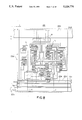
- FIG. 9 showing an example of layout of unit blocks on a semiconductor chip 20.
- the chip 20 has a chip area 21 defined by an input/output region 21a which may include input/output buffer circuits and terminal pads, and a number of aggregation of unit blocks or mini-macro blocks 23 each including a number of unit blocks 22 assembled therein, are disposed on the chip area 21.
- a plurality of unit blocks 22 are arranged adjacent to each other in the Y-direction, and such that the short, lateral side edges of the unit blocks are aligned in the Y-direction.
- the number of unit blocks included in one mini-macro block 23 may be changed in each mini-macro block. In other words, the mini-macro block 23 may have various sizes in the Y-direction.
- the size of the mini-macro block 23 in the X-direction is identical throughout and agrees with the standardized size L of the unit block 22. Further, there may be provided a mega-cell region 24 of rectangular shape for function blocks such as RAM, ROM or ALU with a size increased as compared to the unit block 22.
- the mini-macro block 23 may be divided into a plurality of mini-macro blocks as desired whenever it is desired to have a space for interconnection.
- the mini-macro blocks 23 are disposed on the chip 20 such that a number of channel regions 25 are formed between adjacent mini-macro blocks 23.
- the mini-macro blocks 23 are disposed freely on the chip area 21 except for the orientation such that the unit blocks 22 in the mini-macro blocks 23 extend always in the X-direction throughout the chip 20.
- some of the mini-macro blocks 23 may be provided isolated from each other as in the case of a mini-macro block 23a while some other mini-macro blocks 23 are provided as a cluster of two or more mini-macro blocks 23 disposed adjacent to each other in the X-direction.
- mini-macro blocks 23b and 23c or mini-macro blocks 23d and 23e disposed adjacent to each other.
- the size of each of the adjacent mini-macro blocks does not necessarily have to be identical.
- mini-macro blocks 23 are assembled and interconnected with each other to form a macro-block 100 which forms a completed functional block or unit of the chip such as ALU and the like. As already noted, a single mini-macro block 23 on the contrary does not usually have the function of such completed functional block.
- One essential feature of the present invention is that there are a plurality of mini-macro blocks 23 in the X-direction with or without channel areas 25 intervening therebetween.
- the only constraint with respect to the arrangement of the mini-macro block 23 and thus the arrangement of the macro-block 100 is that the direction of the unit blocks must be the same throughout the mini-macro blocks 23 and thus throughout the macro-blocks 100 on the chip area 21.
- each of the unit blocks 22 the interconnection between the polycells 22a is completed except for terminals for connection to other polycells in other unit blocks 22. Further, in each of the mini-macro blocks 23, the interconnection between the unit blocks 22 included therein is completed except for terminals for connection to other unit blocks 22 in other mini-macro blocks 23.
- the interconnections critical to the operational speed of the ECL gate is confined within each unit block and thus within each mini-macro block 23 with a minimized length, and thereby a maximum operational speed is guaranteed for the integrated circuit.
- the other interconnections for connecting unit blocks 22 belonging to different mini-macro blocks 23 are provided using a space called channel area or global channel 25 formed between the mini-macro blocks 23.
- FIG. 10A shows an example of interconnections provided in the integrated circuit of the present invention.
- the integrated circuit comprises a number of unit blocks 22 1 , 22 2 , 22 3 , etc. forming the mini-macro blocks 23, and the global channel 25 is formed between the adjacent mini-macro blocks 23.
- the interconnection is completed by conductor patterns not illustrated at a first level below the level of the power conductors 22b and 22c, and a terminal T is provided for interconnection to other polycells 22a.
- These terminals T formed in the polycells 22a in the unit blocks 22 1 , 22 2 , 22 3 are connected to each other by an interconnection conductor pattern 22x provided at a third level above the level, or a second level, of the power conductors 22b and 22c.
- the conductor pattern 22x is used for interconnection which is critical to the high speed operation of the integrated circuit.
- another interconnection pattern 25x in correspondence to the global channel 25 at the first or second level for the interconnection between the polycells 22a that belong to different mini-macro blocks 23. This interconnection pattern 25x is used for the interconnections less critical to the high speed operation of the integrated circuit.
- the polycells 22a forming the logic circuits which are critical to the high speed operation of the integrated circuit are assembled close to each other in each mini-macro block 23 at the time of designing the arrangement of the unit blocks 22 1 , 22 2 , 22 3 .
- FIG. 10B shows a typical example of interconnection provided in the conventional CMOS or MOS integrated circuits having the polycell structure, for the purpose of comparison.
- the polycells are arranged into a number of polycell columns 16 as already described with reference to FIG. 2, and the interconnection is achieved by using the interconnection patterns 22x for interconnection of polycells adjacent to each other as well as using the interconnection patterns 25x for connecting polycells which are separated from each other for a relatively long distance.
- each of the polycells in the polycell column is formed with a feed through channel region CH which occupies a substantial area of the polycell. Note that FIGS. 10A and 10B are drawn with substantially the same scale.
- the design and layout of the macro-blocks 100 can be performed efficiently by automatic design procedure such as CAD.
- the design of integrated circuit using the concept of unit blocks 22 and macro-blocks 100 formed from the unit blocks 22 in the form of an assembly of mini-macro blocks 23 as disclosed in the present invention is suited for application of automatic design procedure.
- this structure of the present invention enables the application of a hierarchical CAD method, wherein the timing as well as layout designing of the integrated circuit can be performed in different hierarchical levels, one hierarchical level corresponding to the layout inside the macro-blocks 100, and the other hierarchical levels for the mutual layout of the individual macro-blocks 100.
- the designing process By separating the designing process as such, various advantageous features such as the minimization of layout correction, early feedback to the logic as well as timing simulation, reduction of the computer load for designing, and the like are achieved as will be described.
- mega-cell structures 24 such as RAM, ROM or ALU can be provided at any desired location on the chip area 21.
- the electric power needed in a unit area on the chip 20 is maintained almost constant when the integrated circuit is constructed using the unit blocks 22 or mini-macro blocks 23 of the present invention.
- the average electric power to be fed into a unit area of the chip area 21 remains substantially constant as long as the unit blocks 22 are distributed substantially uniformly over the chip area 21.
- feeding of electric power to the integrated circuit can be achieved using a fixed power feed system. Various examples of such a fixed power feed system will be described later.
- FIG. 11 shows a second embodiment wherein the global channel 25 formed between a pair of mini-macro blocks 23 has a constant width W CH throughout the chip area 21 and the global channel 25 extends straight in the Y-direction throughout the chip area 21.
- a number of mini-macro blocks 23 are arranged into a group of mini-macro block columns 23 1 , 23 2 , 23 3 , and the like, each extending straight in the Y-direction.
- mini-macro block columns 23 1 , 23 2 , 23 3 one or more mini-macro blocks 23 having various sizes in the Y-direction are included.
- Such a regular layout of mini-macro block columns 23 1 , 23 2 , 23 3 makes it possible to use a regular power feed pattern which is extremely advantageous for feeding a large electric power. In the following description, feeding of electric power to the integrated circuit will be described.
- FIG. 12A shows a construction of power feed system for feeding the electric power in the case of the second embodiment shown in FIG. 11 wherein there are a number of parallel, straight global channels 25 repeated with a predetermined interval equal to the length L of the unit blocks 22.
- power buses 30 1 , 30 2 , 30 3 , etc. are provided in correspondence to global channels 25 1 , 25 2 , 25 3 and the like, and these power buses are connected commonly to the corresponding power conductors 22b and 22c of the unit blocks 22 included in the mini-macro block columns 23 1 , 23 2 , and the like at the intersections to these power conductors.
- the power conductors 22b and 22c are provided at the second level above the first level used for interconnections completing within the unit block 22 as shown schematically in FIG. 12B while the power buses 30 1 , 30 2 and 30 3 are provided at the third level above the second level.
- an interconnection conductor 22x 1 extending in the X-direction and another interconnection conductor 22x 2 extending in the Y-direction are also shown.
- These interconnection conductors 22x 1 and 22x 2 form the foregoing conductor pattern 22x, wherein the conductor 22x 1 is provided at the second level and the conductor 22x 2 is provided at the third level.
- the power buses 30 1 and 30 2 are connected respectively to the power conductors 22b and 22C of one unit block 22 and the power buses 30 2 and 30 3 are connected respectively to the power conductors 22b' and 22c' of an adjacent unit block 22'.
- the power buses 30 1 -30 3 are supplied with electric power corresponding to the source voltages V CC and V EE from main power buses 31 1 and 31 2 provided at a fourth level so as to extend in the X-direction alternately, through power via-holes Power Via at the intersection of power buses and the main power buses.
- the first, second, third and fourth level conductors are separated from each other by insulator layers not illustrated.
- the fourth level of the conductor layer on the chip is covered substantially completely by the main power buses and an extremely powerful power feed system is constructed.
- any of the unit blocks 22 on the chip 20 is connected to a suitable pair of the power buses 30 1 , 30 2 , 30 3 , . . . wherever it may be provided on the chip area 21 and supply of sufficient electric power is guaranteed.
- the illustrated construction is for feeding the source voltages V EE and V CC
- the present power feed system can be easily modified to the case where three or more source voltages are supplied by increasing the number of power buses or power conductors in each level of conductor layers.
- the first level of the global channels can be used freely for interconnection 25x (FIG. 10A) between the polycells in the different mini-macro blocks 23 and the degree of freedom for designing the integrated circuit is substantially increased. Further, interconnections between different unit blocks 22 in a single mini-macro block 23 can be made freely by providing interconnection conductors 22x (FIG. 10A) extending in the Y-direction at the second level.
- the pitch of repetition of the power buses 30 1 -30 3 in the X-direction is set slightly larger than the size L of the unit block 22 in correspondence to the pitch of repetition of the global channels 25 1 -25 3 which is equal to the sum of the size L and the width W CH of the global channels.
- the mini-macro blocks 23 and 23' are arranged adjacent to each other in the Y-direction with a mutual offset in the X-direction.
- the global channels 25 at both sides of the mini-macro blocks 23 and 23' extend no longer straight throughout the chip area 21.
- power buses are provided in correspondence to each area 25 between a pair of mini-macro blocks 23, 23' and the like as shown in FIG. 13 by power buses 30 1 , 30 1 ', 30 2 , 30 2 ' and the like, and feeding of the electric power is made to these power buses from the main power buses 31 1 and 31 2 which are provided in the X-direction similarly to the case of FIG. 12A.
- the pitch of repetition P1 of the main power buses 31 1 and 31 2 is set smaller than the minimum height H 23 of the mini-macro blocks existing in the chip area 21.
- the pitch P1 is the sum of the width of the conductor strips forming the main power bus 31 1 and the main power bus 31 2 .
- the layout process of mini-macro blocks 23 on the chip area 21 can be performed freely and efficiently by CAD without particular consideration about the power feed system. Thereby, detailed design such as routing of wiring conductors becomes substantially easier.
- FIG. 14 shows another example of power feed system.
- This example corresponds to the case where the mini-macro blocks 23 are disposed freely on the chip area 21 as in the case of the first embodiment shown in FIG. 9, and the main power buses 31 1 and 31 2 are provided in the Y-direction.
- the power buses 30 1 and 30 2 are eliminated and the main power buses 31 1 and 31 2 make a direct contact to the power conductors 22b and 22c of the unit blocks 22.
- any one of the unit blocks in the mini-macro blocks 23 is crossed by a pair of main power buses 31 1 and 31 2 wherever the mini-macro blocks may be provided, and feeding of electric power to any of the unit blocks 22 in any of the mini-macro blocks 23 can be achieved through power via-holes Power Via shown in FIG. 14.
- FIG. 15 shows a third embodiment of the integrated circuit wherein different types of unit blocks 22 1 and 22 2 having different standardized heights H 22a , H 22b are provided on the chip area 21 to form various mini-macro blocks 23, 23', 23" and the like. There may be even isolated unit blocks 22 not forming the mini-macro blocks.
- the power conductors at the top and bottom edges of the unit blocks are omitted from illustration. Such a construction is preferred when various different type of polycells different in the function and size have to be used in one chip.
- the polycells are classified into a number of groups each having respective heights H such as height H 22a , H 22b and the unit block is constructed by assembling polycells having a common height.
- the unit blocks 22 1 , 22 2 having respective heights, although the length L of the unit block in the X-direction is maintained constant.
- the layout process can be performed easily by CAD. Even in this case, it should be noted that the power density or electric power to be supplied to a unit area on the chip is maintained substantially constant.
- the power feeding systems described with reference to FIGS. 13 and 14 are effective also in this case.
- FIGS. 16 shows a fourth embodiment of the integrated circuit according to the present invention.
- illustration of the parallel power conductors 22b, 22c will be omitted.
- the degree of freedom about the size of the unit blocks is further increased such that the size measured in the X-direction of the unit blocks can be optimized in each unit block.
- each of the polycells in one unit block has a same height H in the Y-direction but this height may vary when the unit block is different.
- different types of mini-macro blocks 23, 23' and 23" having respective lengths in the X-direction are formed by assembling unit blocks 22 1 , 22 2 , 22 3 , 22 1 ', 22 2 ', 22 3 ', 22 1 ", 22 2 ", 22 3 " having various lengths in the X-direction and various heights in the Y-direction according to the length.
- the unit blocks 22 1 , 22 2 , 22 3 have a same length L 23 throughout
- the unit blocks 22 1 ', 22 2 ', 22 3 ' have a same length L 23a throughout
- the unit blocks 22 1 ", 22 2 “, 22 3 " have a same length L 23b throughout.
- the mini-macro block units 23, 23' and 23" have respective heights H 23 , H 23a and H 23b which may be different from each other.
- the height H 23 of the mini-macro block unit 23 and the height H 23a of the mini-macro block unit 23' are identical to each other while the height H 23b of the mini-macro block unit 23" is different.
- FIG. 16 further shows an example of power feeding system applied to this embodiment.
- This power feeding system is also applicable to the embodiment of FIG. 15.
- the power feeding system is substantially identical to that of FIG. 13 wherein two different main power buses 31 1 and 31 2 are provided parallel and adjacent to each other in the X-direction.
- the pitch of repetition of the power buses 31 1 and 31 2 is set to a value P3 which satisfies a relation:
- the pitch P3 is set smaller than the minimum height of the mini-macro block unit in the chip.
- any one of the mini-macro blocks is supplied with the power from a pair of main power buses 31 1 and 31 2 .
- FIG. 17 shows a fifth embodiment of the present invention.
- unit blocks having different sizes in the X-direction and different heights in the Y-direction are assembled freely to form the mini-macro blocks.
- the side edges of the mini-macro blocks in the Y-direction are not always straight.
- fixed power feed system can be applied by arranging power buses 30 1 and 30 2 side by side in the Y-direction with a pitch of repetition P4 set smaller than the minimum length L of the unit blocks therein.
- the pitch P4 is set such that
- L 23c , L 23d , L 23e represent the size of the mini-macro blocks in the X-direction
- L min represents the minimum length of the unit block or mini-macro block unit in the X-direction existing on the chip.
- FIGS. 18 and 19 show the example of feeding electric power to the mega-cell 24 shown in FIG. 9.
- the power buses 30 1 and 30 2 are provided in correspondence to the global channels 25 at both sides of the mini-macro block units 23 similarly to the case of foregoing embodiments, and the feeding of electric power is made by providing the main power buses 31 1 and 31 2 in the X-direction similarly to the embodiments of FIGS. 12A, 13 and 16.
- the mega-cell 24 may form functional unit such as RAM, ROM or ALU as already described, and has a size substantially larger than that of the unit block 22.
- a power conductor 24a and a power conductor 24b are provided on the mega-cell 24 generally in the Y-direction and the electric power is fed to the mega-cell 24 through power via-holes at the intersection of the power conductors 24a, 24b and the power buses 31 1 and 31 2 .
- the pitch of repetition of the power buses 31 1 and 31 2 in the direction Y to a pitch P5 which is equal to or smaller than the length L V of the power conductors 24a and 24b measured in the Y-direction, the electric power can be supplied reliably to the power conductors 24a and 24b from the power buses 31 1 and 31 2 wherever the mega-cell 24 may be provided on the chip area 21.
- FIG. 19 shows a case for feeding the electric power to the mega-cell 24 from power buses 31 1 and 31 2 extending in the Y-direction through power conductors 24a and 24b which are now extending in the X-direction.
- FIGS. 20A and 20B are flowcharts showing the layout process applied to the semiconductor integrated circuit of the present invention.
- a schematic circuit diagram of the logic circuit to be formed on the chip 20 is given, and a logic simulation as well as a timing simulation are conducted for this logic circuit in a subsequent step 2.
- a hierarchical logic net list data representing a primal interconnection of the logic circuit is extracted, and in a step 4, the logic circuit is expanded into various hierarchical levels using the extracted logic net list data.
- parameters such as the critical path, type and number of the functional blocks formed on the chip and the like are produced.
- the steps 1 through 3 are common to the conventional steps of designing the semiconductor integrated circuits.
- the steps 4 and 5 are the interface steps to make the data fit to the layout system and to prepare instruction data to control the layout and to achieve a tuned performance.
- step 6 the chip floor plan or layout in the hierarchical level of the macro-blocks is started.
- the size and construction of the macro-blocks 100 is estimated, using the boundary data of various fundamental gates and devices used in the macro-blocks 100. These semiconductor patterns are available from the cell library.
- a step 7 an initial placement of the megacells 24 and macro-blocks 100 is performed.
- a step 8 following thereto, an estimation is made for the necessary global channels 25 on the basis of the initial layout of the step 7.
- a step 9 performed in parallel to the step 8, an estimation is made for necessary global feed-through channels to be provided in the macro-blocks.
- an analysis for the delay of signals transferred through the global channels 25 and as well as for the drivability of the various logic gates used in these global net driving is performed in a step 10, taking the estimated delay of signals into consideration.
- step 10 the logic simulation as well as the timing simulation of the step 2 is performed again and the steps from the step 3 through step 10 are repeated until the drivability of the logic circuit is confirmed.
- the result of analysis in the step 10 is fed back to a step 12 where a modification of the placement of the macro-blocks is made.
- step 11 an analysis is made in a step 11, which is performed parallel to the steps 8 and 9, for the necessary current and voltage drop at the time of supplying the power to each of the logic gates in the macro-blocks 100.
- modification of the placement of the macro-blocks is made in the step 12, and the steps 8 through 11 are repeated until the supply of necessary current with an allowable voltage drop is reached.
- the unit blocks 22 and the mini-macro blocks 23 are placed in the macro-blocks 100 in a step 14, the feed-through path is provided in the macro-blocks 100 in a step 14, the input/output cells are provided on the macro-blocks 100 in a step 15, the internal cells of the macro-blocks 100 are placed in a step 16, and the internal connections in the macro-blocks 100 are completed in a step 17.
- the semiconductor pattern stored in the cell library is utilized.
- the steps 14 through 17 represent the layout inside the macro-blocks 100.
- the macro-block patterns thus completed is replaced by the previously used macro-block patterns in a step 18 and the steps 7 through 11 are repeated until the layout for all the macro-blocks 100 is completed in a step 13.
- the global routing is performed in a step 19 using the global channels 25 and the macro-block feed-through channels generated in the step 9, and the mask data is generated in a step 21 on the basis of the pattern thus obtained.
- Another step 20 for optional pattern generation for compensating voltage drops may be provided between the step 19 and the step 21.
Landscapes
- Engineering & Computer Science (AREA)
- Power Engineering (AREA)
- Microelectronics & Electronic Packaging (AREA)
- Physics & Mathematics (AREA)
- Condensed Matter Physics & Semiconductors (AREA)
- General Physics & Mathematics (AREA)
- Computer Hardware Design (AREA)
- Ceramic Engineering (AREA)
- Manufacturing & Machinery (AREA)
- Design And Manufacture Of Integrated Circuits (AREA)
- Semiconductor Integrated Circuits (AREA)
Abstract
Description
P3<H.sub.23a
P3<H.sub.23b
P4<L23c
P4<L.sub.23d
P4<L.sub.23e
. . .
P4<L.sub.min
Claims (22)
Applications Claiming Priority (4)
| Application Number | Priority Date | Filing Date | Title |
|---|---|---|---|
| JP1-61818 | 1989-03-14 | ||
| JP6181889 | 1989-03-14 | ||
| JP8191789 | 1989-03-31 | ||
| JP1-81917 | 1989-03-31 |
Publications (1)
| Publication Number | Publication Date |
|---|---|
| US5124776A true US5124776A (en) | 1992-06-23 |
Family
ID=26402900
Family Applications (1)
| Application Number | Title | Priority Date | Filing Date |
|---|---|---|---|
| US07/492,898 Expired - Lifetime US5124776A (en) | 1989-03-14 | 1990-03-13 | Bipolar integrated circuit having a unit block structure |
Country Status (3)
| Country | Link |
|---|---|
| US (1) | US5124776A (en) |
| EP (1) | EP0387812A3 (en) |
| KR (1) | KR930003838B1 (en) |
Cited By (13)
| Publication number | Priority date | Publication date | Assignee | Title |
|---|---|---|---|---|
| US5208469A (en) * | 1990-07-06 | 1993-05-04 | Fujitsu Limited | Wafer scale integrated circuit and method of forming signal propagation path therein |
| DE4414353A1 (en) * | 1993-05-31 | 1994-12-01 | Fujitsu Ltd | Integrated semiconductor circuit with regularly arranged transistor base cells |
| US5671397A (en) * | 1993-12-27 | 1997-09-23 | At&T Global Information Solutions Company | Sea-of-cells array of transistors |
| US5844262A (en) * | 1995-05-25 | 1998-12-01 | Mitsubishi Denki Kabushiki Kaisha | Semiconductor device for reducing effects of noise on an internal circuit |
| US20020145444A1 (en) * | 2001-04-04 | 2002-10-10 | Nec Corporation | Semi-custom-made semiconductor integrated circuit device, method for customization and method for redesign |
| US20030135837A1 (en) * | 2002-01-17 | 2003-07-17 | Hideyuki Okabe | Method and apparatus for automatic arrangement and wiring for a semiconductor integrated circuit design and wiring program therefor |
| US6675361B1 (en) | 1993-12-27 | 2004-01-06 | Hyundai Electronics America | Method of constructing an integrated circuit comprising an embedded macro |
| US20040164303A1 (en) * | 2000-09-29 | 2004-08-26 | Katsuya Anzai | Contact between element to be driven and thin film transistor for supplying power to element to be driven |
| US20050022146A1 (en) * | 2001-04-23 | 2005-01-27 | Telairity Semiconductor, Inc. | Circuit group design methodologies |
| US20050138595A1 (en) * | 2003-12-18 | 2005-06-23 | Lsi Logic Corporation | System and method for mapping logical components to physical locations in an integrated circuit design environment |
| US20060243955A1 (en) * | 2005-04-19 | 2006-11-02 | Yukihiro Fujimoto | Semiconductor integrated circuit device |
| US20070113210A1 (en) * | 2005-11-16 | 2007-05-17 | Fujitsu Limited | Method and apparatus for supporting verification, and computer product |
| US20110024869A1 (en) * | 2009-07-31 | 2011-02-03 | Nec Electronics Corporation | Design method, design program and design support device for semiconductor integrated circuit, and semiconductor integrated circuit |
Citations (11)
| Publication number | Priority date | Publication date | Assignee | Title |
|---|---|---|---|---|
| JPS5878450A (en) * | 1981-11-04 | 1983-05-12 | Nippon Telegr & Teleph Corp <Ntt> | Semiconductor integrated circuit device |
| JPS59165436A (en) * | 1983-03-11 | 1984-09-18 | Toshiba Corp | Semiconductor integrated circuit device |
| JPS6130050A (en) * | 1984-07-20 | 1986-02-12 | Nec Corp | Integrated logic circuit device |
| US4623911A (en) * | 1983-12-16 | 1986-11-18 | Rca Corporation | High circuit density ICs |
| JPS62166542A (en) * | 1986-01-18 | 1987-07-23 | Fujitsu Ltd | Semiconductor integrated circuit |
| US4716452A (en) * | 1984-11-09 | 1987-12-29 | Kabushiki Kaisha Toshiba | Semiconductor integrated circuit device constructed by polycell technique |
| JPS63283038A (en) * | 1987-05-14 | 1988-11-18 | Mitsubishi Electric Corp | Semiconductor integrated circuit |
| US4833520A (en) * | 1986-01-22 | 1989-05-23 | Nec Corporation | Semiconductor integrated circuit having wirings for power supply suited for computer-aided-design |
| US4841352A (en) * | 1985-11-13 | 1989-06-20 | Nec Corporation | Semi-custom integrated circuit provided with standardized capacitor cells |
| US4870300A (en) * | 1986-08-06 | 1989-09-26 | Mitsubishi Denki Kabushiki Kaisha | Standard cell system large scale integrated circuit with heavy load lines passing through the cells |
| US4893170A (en) * | 1983-06-24 | 1990-01-09 | Mitsubishi Denki Kabushiki Kaisha | Semiconductor device with multi-level wiring in a gate array |
Family Cites Families (4)
| Publication number | Priority date | Publication date | Assignee | Title |
|---|---|---|---|---|
| CA1024661A (en) * | 1974-06-26 | 1978-01-17 | International Business Machines Corporation | Wireable planar integrated circuit chip structure |
| DE2643482A1 (en) * | 1976-09-27 | 1978-03-30 | Siemens Ag | SEMI-CONDUCTOR PLATE FOR MANUFACTURING HIGHLY INTEGRATED COMPONENTS |
| US4612618A (en) * | 1983-06-10 | 1986-09-16 | Rca Corporation | Hierarchical, computerized design of integrated circuits |
| JPS63152144A (en) * | 1986-12-17 | 1988-06-24 | Hitachi Ltd | Semiconductor integrated circuit device |
-
1990
- 1990-03-13 EP EP19900104756 patent/EP0387812A3/en not_active Ceased
- 1990-03-13 US US07/492,898 patent/US5124776A/en not_active Expired - Lifetime
- 1990-03-14 KR KR1019900003413A patent/KR930003838B1/en not_active IP Right Cessation
Patent Citations (11)
| Publication number | Priority date | Publication date | Assignee | Title |
|---|---|---|---|---|
| JPS5878450A (en) * | 1981-11-04 | 1983-05-12 | Nippon Telegr & Teleph Corp <Ntt> | Semiconductor integrated circuit device |
| JPS59165436A (en) * | 1983-03-11 | 1984-09-18 | Toshiba Corp | Semiconductor integrated circuit device |
| US4893170A (en) * | 1983-06-24 | 1990-01-09 | Mitsubishi Denki Kabushiki Kaisha | Semiconductor device with multi-level wiring in a gate array |
| US4623911A (en) * | 1983-12-16 | 1986-11-18 | Rca Corporation | High circuit density ICs |
| JPS6130050A (en) * | 1984-07-20 | 1986-02-12 | Nec Corp | Integrated logic circuit device |
| US4716452A (en) * | 1984-11-09 | 1987-12-29 | Kabushiki Kaisha Toshiba | Semiconductor integrated circuit device constructed by polycell technique |
| US4841352A (en) * | 1985-11-13 | 1989-06-20 | Nec Corporation | Semi-custom integrated circuit provided with standardized capacitor cells |
| JPS62166542A (en) * | 1986-01-18 | 1987-07-23 | Fujitsu Ltd | Semiconductor integrated circuit |
| US4833520A (en) * | 1986-01-22 | 1989-05-23 | Nec Corporation | Semiconductor integrated circuit having wirings for power supply suited for computer-aided-design |
| US4870300A (en) * | 1986-08-06 | 1989-09-26 | Mitsubishi Denki Kabushiki Kaisha | Standard cell system large scale integrated circuit with heavy load lines passing through the cells |
| JPS63283038A (en) * | 1987-05-14 | 1988-11-18 | Mitsubishi Electric Corp | Semiconductor integrated circuit |
Cited By (36)
| Publication number | Priority date | Publication date | Assignee | Title |
|---|---|---|---|---|
| US5208469A (en) * | 1990-07-06 | 1993-05-04 | Fujitsu Limited | Wafer scale integrated circuit and method of forming signal propagation path therein |
| US5694078A (en) * | 1993-05-31 | 1997-12-02 | Fujitsu Limited | Semiconductor integrated circuit having regularly arranged transistor basic cells |
| DE4414353A1 (en) * | 1993-05-31 | 1994-12-01 | Fujitsu Ltd | Integrated semiconductor circuit with regularly arranged transistor base cells |
| US7207025B2 (en) | 1993-12-27 | 2007-04-17 | Magnachip Semiconductor, Ltd. | Sea-of-cells array of transistors |
| US6977399B2 (en) | 1993-12-27 | 2005-12-20 | Hynix Semiconductor Inc. | Sea-of-cells array of transistors |
| US5869900A (en) * | 1993-12-27 | 1999-02-09 | At&T Global Information Solutions Company | Sea-of-cells array of transistors |
| US5671397A (en) * | 1993-12-27 | 1997-09-23 | At&T Global Information Solutions Company | Sea-of-cells array of transistors |
| US7257779B2 (en) | 1993-12-27 | 2007-08-14 | Magnachip Semiconductor, Ltd. | Sea-of-cells array of transistors |
| US6269466B1 (en) | 1993-12-27 | 2001-07-31 | Hyundai Electronics America | Method of constructing an integrated circuit utilizing multiple layers of interconnect |
| US6489641B1 (en) | 1993-12-27 | 2002-12-03 | Hyundai Electronics America | Sea-of-cells array of transistors |
| US6967361B2 (en) | 1993-12-27 | 2005-11-22 | Magnachip Semiconductor, Ltd. | Sea-of-cells array of transistors |
| US6605499B1 (en) | 1993-12-27 | 2003-08-12 | Hyundai Electronics America, Inc. | Method of forming sea-of-cells array of transistors |
| US6675361B1 (en) | 1993-12-27 | 2004-01-06 | Hyundai Electronics America | Method of constructing an integrated circuit comprising an embedded macro |
| US20040005738A1 (en) * | 1993-12-27 | 2004-01-08 | Hyundai Electronics America | Sea-of-cells array of transistors |
| US20040039998A1 (en) * | 1993-12-27 | 2004-02-26 | Crafts Harold S. | Sea-of-cells array of transistors |
| US20040078769A1 (en) * | 1993-12-27 | 2004-04-22 | Crafts Harold S. | Sea-of-cells array of transistors |
| US5844262A (en) * | 1995-05-25 | 1998-12-01 | Mitsubishi Denki Kabushiki Kaisha | Semiconductor device for reducing effects of noise on an internal circuit |
| US6331719B2 (en) | 1995-05-25 | 2001-12-18 | Mitsubishi Denki Kabushiki Kaisha | Semiconductor device for reducing effects of noise on an internal circuit |
| US20040164303A1 (en) * | 2000-09-29 | 2004-08-26 | Katsuya Anzai | Contact between element to be driven and thin film transistor for supplying power to element to be driven |
| US7102163B2 (en) | 2000-09-29 | 2006-09-05 | Sanyo Electric Co., Ltd. | Contact between element to be driven and thin film transistor for supplying power to element to be driven |
| US7523436B2 (en) | 2001-04-04 | 2009-04-21 | Nec Electronics Corporation | Semi-custom-made semiconductor integrated circuit device, method for customization and method for redesign |
| US20020145444A1 (en) * | 2001-04-04 | 2002-10-10 | Nec Corporation | Semi-custom-made semiconductor integrated circuit device, method for customization and method for redesign |
| US7047514B2 (en) * | 2001-04-04 | 2006-05-16 | Nec Electronics Corporation | Semi-custom-made semiconductor integrated circuit device, method for customization and method for redesign |
| US20060189041A1 (en) * | 2001-04-04 | 2006-08-24 | Nec Electronics Corporation | Semi-custom-made semiconductor integrated circuit device, method for customization and method for redesign |
| US20050022146A1 (en) * | 2001-04-23 | 2005-01-27 | Telairity Semiconductor, Inc. | Circuit group design methodologies |
| US20050028128A1 (en) * | 2001-04-23 | 2005-02-03 | Telairity Semiconductor, Inc. | Circuit group design methodologies |
| US7234123B2 (en) | 2001-04-23 | 2007-06-19 | Telairity Semiconductor, Inc. | Circuit group design methodologies |
| US6910199B2 (en) | 2001-04-23 | 2005-06-21 | Telairity Semiconductor, Inc. | Circuit group design methodologies |
| US20030135837A1 (en) * | 2002-01-17 | 2003-07-17 | Hideyuki Okabe | Method and apparatus for automatic arrangement and wiring for a semiconductor integrated circuit design and wiring program therefor |
| US7269803B2 (en) * | 2003-12-18 | 2007-09-11 | Lsi Corporation | System and method for mapping logical components to physical locations in an integrated circuit design environment |
| US20050138595A1 (en) * | 2003-12-18 | 2005-06-23 | Lsi Logic Corporation | System and method for mapping logical components to physical locations in an integrated circuit design environment |
| US20060243955A1 (en) * | 2005-04-19 | 2006-11-02 | Yukihiro Fujimoto | Semiconductor integrated circuit device |
| US7478358B2 (en) * | 2005-04-19 | 2009-01-13 | Kabushiki Kaisha Toshiba | Semiconductor integrated circuit device |
| US20070113210A1 (en) * | 2005-11-16 | 2007-05-17 | Fujitsu Limited | Method and apparatus for supporting verification, and computer product |
| US20110024869A1 (en) * | 2009-07-31 | 2011-02-03 | Nec Electronics Corporation | Design method, design program and design support device for semiconductor integrated circuit, and semiconductor integrated circuit |
| US8187924B2 (en) | 2009-07-31 | 2012-05-29 | Renesas Electronics Corporation | Method, design program and design support device for semiconductor integrated circuit, and semiconductor integrated circuit |
Also Published As
| Publication number | Publication date |
|---|---|
| KR900015349A (en) | 1990-10-26 |
| EP0387812A3 (en) | 1992-08-05 |
| EP0387812A2 (en) | 1990-09-19 |
| KR930003838B1 (en) | 1993-05-13 |
| JPH0316155A (en) | 1991-01-24 |
Similar Documents
| Publication | Publication Date | Title |
|---|---|---|
| USRE39469E1 (en) | Semiconductor integrated circuit with mixed gate array and standard cell | |
| US6938226B2 (en) | 7-tracks standard cell library | |
| US6404226B1 (en) | Integrated circuit with standard cell logic and spare gates | |
| US5124776A (en) | Bipolar integrated circuit having a unit block structure | |
| US5095352A (en) | Semiconductor integrated circuit device of standard cell system | |
| EP0360507B1 (en) | Semiconductor integrated circuit device having an improved arrangement of power source lines | |
| EP0167365B1 (en) | Standard cell lsis | |
| US6967361B2 (en) | Sea-of-cells array of transistors | |
| US7257779B2 (en) | Sea-of-cells array of transistors | |
| US5388055A (en) | Semiconductor integrated circuit having polycell structure and method of designing the same | |
| KR20010029851A (en) | Standard cell, standard cell array, and system and method for placing and routing standard cells | |
| US4499484A (en) | Integrated circuit manufactured by master slice method | |
| JPH10335612A (en) | High density gate array cell structure and its manufacture | |
| US6560753B2 (en) | Integrated circuit having tap cells and a method for positioning tap cells in an integrated circuit | |
| EP0072674B1 (en) | A semiconductor device having a gate array structure | |
| KR950013740B1 (en) | Semiconductor integrated circuit | |
| EP0021661A1 (en) | Semiconductor master-slice device | |
| US6781170B2 (en) | Integrated circuit base transistor structure and associated programmable cell library | |
| US6842886B2 (en) | Basic cell of gate array semiconductor device, gate array semiconductor device, and layout method for gate array semiconductor device | |
| JP3027757B2 (en) | Semiconductor integrated circuit | |
| JP6836137B2 (en) | Semiconductor device and its layout design method | |
| JPS6135534A (en) | Wiring system for feeder and signal wire of lsi |
Legal Events
| Date | Code | Title | Description |
|---|---|---|---|
| AS | Assignment |
Owner name: FUJITSU LIMITED, JAPAN Free format text: ASSIGNMENT OF ASSIGNORS INTEREST.;ASSIGNORS:TANIZAWA, TETSU;DOI, TAKEHITO;TOKUDA, HIDEO;AND OTHERS;REEL/FRAME:005257/0650 Effective date: 19900310 Owner name: FUJITSU VLSI LIMITED, JAPAN Free format text: ASSIGNMENT OF ASSIGNORS INTEREST.;ASSIGNORS:TANIZAWA, TETSU;DOI, TAKEHITO;TOKUDA, HIDEO;AND OTHERS;REEL/FRAME:005257/0650 Effective date: 19900310 |
|
| STCF | Information on status: patent grant |
Free format text: PATENTED CASE |
|
| FEPP | Fee payment procedure |
Free format text: PAYOR NUMBER ASSIGNED (ORIGINAL EVENT CODE: ASPN); ENTITY STATUS OF PATENT OWNER: LARGE ENTITY |
|
| CC | Certificate of correction | ||
| FPAY | Fee payment |
Year of fee payment: 4 |
|
| FPAY | Fee payment |
Year of fee payment: 8 |
|
| FPAY | Fee payment |
Year of fee payment: 12 |
|
| AS | Assignment |
Owner name: FUJITSU MICROELECTRONICS LIMITED, JAPAN Free format text: ASSIGNMENT OF ASSIGNORS INTEREST;ASSIGNOR:FUJITSU LIMITED;REEL/FRAME:022240/0964 Effective date: 20090123 Owner name: FUJITSU MICROELECTRONICS LIMITED,JAPAN Free format text: ASSIGNMENT OF ASSIGNORS INTEREST;ASSIGNOR:FUJITSU LIMITED;REEL/FRAME:022240/0964 Effective date: 20090123 |