US5079614A - Gate array architecture with basic cell interleaved gate electrodes - Google Patents
Gate array architecture with basic cell interleaved gate electrodes Download PDFInfo
- Publication number
- US5079614A US5079614A US07/588,638 US58863890A US5079614A US 5079614 A US5079614 A US 5079614A US 58863890 A US58863890 A US 58863890A US 5079614 A US5079614 A US 5079614A
- Authority
- US
- United States
- Prior art keywords
- legs
- basic cells
- diffusion regions
- gate electrode
- pair
- Prior art date
- Legal status (The legal status is an assumption and is not a legal conclusion. Google has not performed a legal analysis and makes no representation as to the accuracy of the status listed.)
- Expired - Lifetime
Links
Images


Classifications
-
- H—ELECTRICITY
- H01—ELECTRIC ELEMENTS
- H01L—SEMICONDUCTOR DEVICES NOT COVERED BY CLASS H10
- H01L27/00—Devices consisting of a plurality of semiconductor or other solid-state components formed in or on a common substrate
- H01L27/02—Devices consisting of a plurality of semiconductor or other solid-state components formed in or on a common substrate including semiconductor components specially adapted for rectifying, oscillating, amplifying or switching and having at least one potential-jump barrier or surface barrier; including integrated passive circuit elements with at least one potential-jump barrier or surface barrier
- H01L27/04—Devices consisting of a plurality of semiconductor or other solid-state components formed in or on a common substrate including semiconductor components specially adapted for rectifying, oscillating, amplifying or switching and having at least one potential-jump barrier or surface barrier; including integrated passive circuit elements with at least one potential-jump barrier or surface barrier the substrate being a semiconductor body
- H01L27/10—Devices consisting of a plurality of semiconductor or other solid-state components formed in or on a common substrate including semiconductor components specially adapted for rectifying, oscillating, amplifying or switching and having at least one potential-jump barrier or surface barrier; including integrated passive circuit elements with at least one potential-jump barrier or surface barrier the substrate being a semiconductor body including a plurality of individual components in a repetitive configuration
- H01L27/118—Masterslice integrated circuits
- H01L27/11803—Masterslice integrated circuits using field effect technology
- H01L27/11807—CMOS gate arrays
Definitions
- This invention relates generally to gate array cell architecture and, more particularly, to CMOS gate array cell architecture for double metal CMOS processing that provides for straight line cell metal interconnects or metal interconnect paths in one metal level between cells for substantially most circuit designs and without the need for separate routing channels.
- the core of a M 2 CMOS gate array comprises the placement of a multitude of gate array basic cells in orthogonal directions, such as, in consecutive rows and/or columns.
- the gate array basic cell per se is generally comprised of two or more n-channel and p-channel transistor pairs.
- a gate array macrocell comprises the interconnection of transistor pairs in one or more basic cells employing metal-1 or M-1 and metal-2 or M-2 interconnect layers. There is a preferred travel direction associated with each of these metal layers so that, for example, M-1 travels only in the vertical direction and M-2 travels only in the horizontal direction or vice versa.
- a circuit design is fulfilled for a gate array by automatically placing the macrocells on possible basic cell sites and routing them together employing two metal interconnect layers.
- the amount of M-1 and M-2 employed in order to build macrocells generally completely covers the entire area of the basic cell thereby leaving no room for metal routing.
- one approach is to provide an area adjacent to the basic cells which is void of any basic cells. This void area is referred to in the art as a routing channel and a gate array constructed with such a channel is generally referred to as a channeled gate array.
- Another approach is to fill the entire array with basic cells, but leave alternate rows or columns of basic cells empty as they become needed for routing. Such as scheme is illustrated in U.S.
- gate array basic cells generally comprise two or more n-channel and p-channel transistor pairs, such as, illustrated in FIG. 1.
- FIG. 1 depicts the physical layout of a typical four transistor gate array basic cell comprising two transistor pairs.
- the source/drain of p-channel transistors 10 are labelled p 1 , p 2 and p 3 and the source/drain of n-channel transistors 12 are labelled n 1 , n 2 and n 3 .
- Polysilicon lines 14 and 16 form the gate electrode structure for the four transistors 10 and 12.
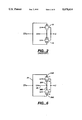
- FIG. 2 illustrates a schematic diagram of a conventional transistor circuit device comprising a CMOS transmission gate pair, which is often employed in gate array macrocells.
- a and B are input signals to transmission gates 16 and 18 which are complementary pairs of CMOS transistors.
- the output of gates 16 and 18 are connected to output Z.
- CK and CK are controlled or clock inputs to drive the gates of the complementary transistor pairs comprising transmission gates 16 and 18 and are determinative of whether either input signal A or input signal B is provided at output Z.
- FIG. 3 is a physical layout of the transistor circuit device of FIG. 2 based on the conventional basic cell of FIG. 1 provided with an interconnect pattern for the transistor circuit device of FIG. 2.
- the metal interconnects require two different levels of metal because there is a necessary change in direction of the metal interconnects to complete the circuit unless one goes outside the basic cell which is not a viable solution because of possible interference with circuitry in an adjacent basic cell.
- FIG. 3 illustrates the complexity of interconnections for forming this circuit device in conventional gate arrays.
- the direction of the first metal layer, M1 is horizontal and the direction of the second metal layer, M2 is vertical.
- the result is that the entire area of the basic cell of FIG. 1 is substantially taken up by the necessary placement of the cell metal interconnects.
- a new basic cell layout employes an interleaved channeless gate array architecture for fabricating very large scale integration circuits created in a gate array that simplifies and minimizes the cell interconnect pattern while leaving ample routing resources without the need for channels or leaving whole rows or columns of transistor portions open or unavailable for use.
- the interleaved channeless gate array architecture of this invention comprises a plurality of rows or columns of basic cells wherein each of the cells includes a pair arrangement of complementary channel MOS transistors formed in adjacently disposed different conductivity type diffusion regions.
- a gate electrode structure for the basic cells comprises a pair of comb-shaped gate electrodes each having a plurality of parallel spatially disposed legs. Gate electrode pairs are formed over each of the basic cells in opposite opposed relation with their legs alternately interleaved relative to each other.
- At least one pair of alternate interleaved legs is formed across each of the basic cell diffusion regions, and metal interconnects are formed across the basic cells in a direction perpendicular relative to direction of the formed interleaved legs, and are contacted to complementary channel MOS transistors and also to the gate electrode legs in gate array basic cells, as required, to form a designated circuit design.
- FIG. 1 is a plane view of a conventional physical layout of a typical gate array basic cell.
- FIG. 2 is an electrical schematic of a transistor circuit device comprising a CMOS transmission gate pair.
- FIG. 3 is a plane view of the conventional physical layout of the gate array basic cell design for the circuit device shown in FIG. 2.
- FIG. 4 is a plane view of the physical layout of the gate array basic cell architecture comprising this invention.
- FIG. 5 is a plane view of the physical layout of the gate array basic cell architecture of this invention for the circuit device shown in FIG. 2.
- FIG. 6 is the circuit device of FIG. 2 illustrating gate and interconnect correspondence with the layout of FIG. 5.
- FIG. 4 illustrates one gate array basic cell comprising, for example, a p + diffusion region 20 and a n + diffusion region 22 from which can be built or created two or more p-channel and n-channel transistor pairs via the regions labeled p 1 , p 2 and p 3 in p + diffusion region 20 of a n-silicon substrate and the regions labeled n 1 , n 2 and n 3 in n + diffusion region 22.
- diffusion regions 20 and 22 are slightly wider in the horizontal or row direction and gate electrode structures 24 and 26 of polysilicon are not formed vertically or in the column direction but rather horizontally in the row direction with extended regions of their structures crossing over diffusion regions 20 and 22.
- gate electrode structures each have multiple leg groups 24A, 24B & 24C, and 26A, 26B & 26C.
- multiple legs 24A, 24B & 24C of gate electrode structure 24 are interleaved with multiple legs 26A, 26B & 26C of gate electrode structure 26.
- at least one pair of spatially disposed legs 24A, 26A of each gate electrode structure 24, 26 are parallel and are formed to longitudinally cross one diffusion region 20.
- each gate electrode structure 24, 26 are parallel and are formed to longitudinally cross the other diffusion region 22.
- Central legs 24C, 26C of gate structures 24, 26 are spatially disposed between diffusion regions 20 and 22 of the basic cell.
- Legs 24C, 26C are regions wherein the metal interconnects may be connected to either polysilicon gate electrode structure 24, 26.
- gate electrode structures 24, 26 comprise comb-shaped gate electrodes having multiple parallel legs 24A-C, 26A-C that are alternately interleaved relative to each other, all run or travel in the horizontal or row direction, and run in opposite directions to form pairs 24A, 26A and 24B, 26B over the longitudinal extent of respective p-type and n-type diffusion regions 20 and 22.
- the comb-shaped electrodes 24, 26 are arranged in oppositely opposed relation to each other with their legs alternately interleaved with each other.
- respective gate pairs 24A, 26A and 24B, 26B define p-channel transistors relative to regions labeled p 1 , p 2 and p 3 and n-channel transistors relative to regions labeled n 1 , n 2 and n 3 .
- the gate array basic cell of FIG. 4 is completed with metal-2, M2, running or traveling horizontally for the VDD power and VSS ground or reference lines, and the respective n + diffusion regions 28, 28A, 28B and p + diffusion regions 30, 30A, 30B that provide for electrical contact to the substrate as well as cell isolation to eliminate latchup.
- the series of vertical lines 32 at the bottom of FIG. 4 and the series of horizontal lines at the right edge of FIG. 4 represent an example of the number of possible metal routing tracks that may be formed in orthogonal directions relative to the gate array basic cell.
- the basic cell architecture of this invention comparatively provides for slightly larger cells over conventional architecture but employs less interconnects to form the circuit connections in both interconnect layers with greater permeability, i.e., greater choice of metal tracks for routing and cell interconnects as represented by lines 32 and 33.
- interconnects may be formed along any track 32 and are all in a single metal travel direction for accommodating almost any type of circuit design or configuration. Since source/drain areas and gate areas run parallel with each other, a single straight line can cross all n-type and p-type source/drain regions n 1 , n 2 and n 3 and p 1 , p 2 and p 3 of a basic cell as well as all as legs and gates 24A-C, 26A-C of polysilicon gate electrode structures 24, 26 of a basic cell.
- any arrangement of source, drain or polysilicon gate in an aligned column of complementary diffusion regions of the gate array can be connected to any other arrangement of source, drain or polysilicon gate of the same column employing a single straight line metal interconnect.
- the example given in the Background of the Invention relative to FIG. 1 was indicated as a connection of areas marked p 1 , p 3 and n 3 . It can be seen that a connection of those same areas p.sub. 1, p 3 and n 3 in FIG. 4 can be accomplished with a single straight line interconnect along one of several tracks 32.
- interleaved gate electrode structures 24, 26 shown in FIG. 4 is just one configuration illustrating the basic principal of this invention.
- gate electrode structures 24, 26 could employ additional leg pairs to cross p + and n + diffusion regions of greater width with individual legs of each pair traveling in opposite directions.
- interconnects could be reversed.
- FIG. 5 illustrates the plane view of the physical layout of the gate array basic cell architecture of this invention, as discussed in FIG. 4 and implemented for the circuit device shown in FIG. 2.
- the metal-1, M1, interconnects 34, 35 and 36 illustrate the simplicity of the interconnect pattern relative to the gate array basic cell employing the architecture of this invention. As illustrated, there is no requirement for a change in metal direction. Also, there is significant room left to route through the cell via other tracks 32 thereby eliminating the need for separate routing channels adjacent to rows or columns of basic cells. Also, all metal-2, M2, tracks 33 are open and available for routing except those taken up by the lines of VDD and VSS. Thus, substantially all the cell interconnections can be accomplished in metal-1, M1.
- Metal-2, M2 is in the other orthogonal direction and thicker and bigger pitch to accommodate the needs for source, VDD, and ground or reference, VSS.
- the same straight line interconnection of designated transistor pairs is also achieved for many other types of gate array devices so that FIG. 5 represents only a single example of the implementation of this invention.
- FIG. 6 shows the electrical schematic diagram for the connected basic cell of FIG. 5 relative to correspondence of diffusion regions p 1 -p 3 and n 1 -n 3 relative gate electrode structures 24, 26 and the two complementary transistor pairs.
- the architecture of this invention minimizes the amount of interconnect metal required to create gate array macrocells because of the simplified interconnected pattern with the travel direction for the interconnects accomplished in a single direction.
- the result interconnect pattern throughout the gate array is greatly simplified without need for metal direction changes.
- Single direction routing of interconnects in M1 due to the interconnect gate electrode structures provides an almost unlimited capability of connecting different areas of diffused source/drain regions of the same or different aligned basic cells to form different kinds of transistor and transistor pair patterns without any requirement for changing the direction of M1 interconnects.
- the foregoing is not meant to be a limitation on the change of direction of interconnect metal, as for a particular application, a change in metal direction can be accomplished via M2.
- the architecture of this invention maximizes gate array macrocell porosity for interconnect routing via both metal layers. Since the number of interconnects throughout the basic cell are minimized, there is a corresponding increase in the amount of parallel interconnect tracks through the basic cell for macrocell connection and interconnection in the gate array. Thus, the possibilities of different routing through the basic cells of the gate array are maximized thereby making it easier for the router or the routing process.
- the architecture of this invention allocates substantial balance of routing resources in both horizontal and vertical directions. This means that there is an even number of potential metal routing tracks throughout the gate array, i.e., before automated interconnect routing but after cell interconnects and power/ground interconnects have been made. This balance is because power distribution is done primarily using M2 and cell interconnect is done primarily using M1.
- the architecture of this invention eliminates the need for routing channels or channel deployment adjacent to aligned gate array basic cells and permits previous channel areas to be employed for basic cell utilization.
- the architecture of this invention achieves very high utilization rates for VLSI devices.
- Prior art approaches of the type previously discussed have utilization rates in the region of 50% of chip real estate.
- the architecture of this invention provides for utilization rates of over 90%.
- the utilization rate of course, depends upon the employment of complement transistor pairs.
- the architecture of this invention permits reduced area per usable gate in the gate array. While the basic cell size is larger than conventional gate array cell sizes, greater utilization rates are achieved due to the interleaved gate electrode structure and simplified cell interconnect pattern. As a result, there is a net reduction in area per useable gate.
- the architecture of this invention permits a reduction in die size with a corresponding reduction in cost and improved device performance.
- the reduction in costs is brought about by smaller dies for circuit design implementation with corresponding reduction in metal line lengths. This will result in smaller scale circuit designs with less capacitance and a corresponding increase in circuit operational speed.
Abstract
Description
Claims (14)
Priority Applications (2)
| Application Number | Priority Date | Filing Date | Title |
|---|---|---|---|
| US07/588,638 US5079614A (en) | 1990-09-26 | 1990-09-26 | Gate array architecture with basic cell interleaved gate electrodes |
| JP3245863A JPH04251976A (en) | 1990-09-26 | 1991-09-25 | Gate array structure |
Applications Claiming Priority (1)
| Application Number | Priority Date | Filing Date | Title |
|---|---|---|---|
| US07/588,638 US5079614A (en) | 1990-09-26 | 1990-09-26 | Gate array architecture with basic cell interleaved gate electrodes |
Publications (1)
| Publication Number | Publication Date |
|---|---|
| US5079614A true US5079614A (en) | 1992-01-07 |
Family
ID=24354682
Family Applications (1)
| Application Number | Title | Priority Date | Filing Date |
|---|---|---|---|
| US07/588,638 Expired - Lifetime US5079614A (en) | 1990-09-26 | 1990-09-26 | Gate array architecture with basic cell interleaved gate electrodes |
Country Status (2)
| Country | Link |
|---|---|
| US (1) | US5079614A (en) |
| JP (1) | JPH04251976A (en) |
Cited By (38)
| Publication number | Priority date | Publication date | Assignee | Title |
|---|---|---|---|---|
| US5691574A (en) * | 1993-09-27 | 1997-11-25 | Nec Corporation | Semiconductor device capable of high speed operation and being integrated with high density |
| US5723883A (en) * | 1995-11-14 | 1998-03-03 | In-Chip | Gate array cell architecture and routing scheme |
| US5859449A (en) * | 1994-08-05 | 1999-01-12 | Mitsubishi Denki Kabushiki Kaisha | Semiconductor integrated circuit |
| US5977810A (en) * | 1997-03-03 | 1999-11-02 | Mitsubishi Denki Kabushiki Kaisha | Clock driver circuit and semiconductor integrated circuit device |
| US6356118B1 (en) * | 1999-04-16 | 2002-03-12 | Hitachi Ltd | Semiconductor integrated circuit device |
| US6362509B1 (en) * | 1999-10-11 | 2002-03-26 | U.S. Philips Electronics | Field effect transistor with organic semiconductor layer |
| US6480059B2 (en) * | 1997-09-30 | 2002-11-12 | Intel Corporation | Method to reduce timing skews in I/O circuits and clock drivers caused by fabrication process tolerances |
| US6603158B1 (en) * | 1999-07-30 | 2003-08-05 | Fujitsu Limited | Semiconductor integrated circuit having high-density base cell array |
| US6617621B1 (en) | 2000-06-06 | 2003-09-09 | Virage Logic Corporation | Gate array architecture using elevated metal levels for customization |
| US6635935B2 (en) * | 2000-07-10 | 2003-10-21 | Mitsubishi Denki Kabushiki Kaisha | Semiconductor device cell having regularly sized and arranged features |
| US6838713B1 (en) | 1999-07-12 | 2005-01-04 | Virage Logic Corporation | Dual-height cell with variable width power rail architecture |
| US20050189569A1 (en) * | 2004-02-16 | 2005-09-01 | Elisabeth Hartwig | Configurable gate array cell with extended poly gate terminal |
| US20060060889A1 (en) * | 2004-09-17 | 2006-03-23 | Hirofumi Uchida | Gate array integrated circuit including a unit cell basic layer having gate terminal regions allowing two contact pads to be disposed laterally |
| US7149142B1 (en) | 2004-05-28 | 2006-12-12 | Virage Logic Corporation | Methods and apparatuses for memory array leakage reduction using internal voltage biasing circuitry |
| EP1739750A2 (en) | 2005-06-07 | 2007-01-03 | Fujitsu Limited | Semiconductor device and writing method for semiconductor device |
| US20070262349A1 (en) * | 2006-05-10 | 2007-11-15 | Jeng-Huang Wu | Common Pass Gate Layout of a D Flip Flop |
| US20080222587A1 (en) * | 2007-03-05 | 2008-09-11 | Tela Innovations, Inc. | Integrated Circuit Cell Library for Multiple Patterning |
| US20090152734A1 (en) * | 2007-12-13 | 2009-06-18 | Tela Innovations, Inc. | Super-Self-Aligned Contacts and Method for Making the Same |
| US20090283915A1 (en) * | 2006-03-09 | 2009-11-19 | Becker Scott T | Oversized Contacts and Vias in Layout Defined by Linearly Constrained Topology |
| US20100031211A1 (en) * | 2008-08-01 | 2010-02-04 | Tela Innovations, Inc. | Methods for Controlling Microloading Variation in Semiconductor Wafer Layout and Fabrication |
| US20100187616A1 (en) * | 2008-03-13 | 2010-07-29 | Tela Innovations, Inc. | Linear Gate Level Cross-Coupled Transistor Device with Overlapping PMOS Transistors and Overlapping NMOS Transistors Relative to Direction of Gate Electrodes |
| US20100277202A1 (en) * | 2006-03-09 | 2010-11-04 | Tela Innovations, Inc. | Circuitry and Layouts for XOR and XNOR Logic |
| US20100287518A1 (en) * | 2009-05-06 | 2010-11-11 | Tela Innovations, Inc. | Cell Circuit and Layout with Linear Finfet Structures |
| US20110084312A1 (en) * | 2009-10-13 | 2011-04-14 | Tela Innovations, Inc. | Methods for Cell Boundary Encroachment and Layouts Implementing the Same |
| US20110108890A1 (en) * | 2007-08-02 | 2011-05-12 | Tela Innovations, Inc. | Semiconductor Device with Dynamic Array Sections Defined and Placed According to Manufacturing Assurance Halos |
| US8032805B1 (en) | 2005-09-12 | 2011-10-04 | Synopsys, Inc. | Input-output device testing including voltage tests |
| US8549455B2 (en) | 2007-08-02 | 2013-10-01 | Tela Innovations, Inc. | Methods for cell phasing and placement in dynamic array architecture and implementation of the same |
| US8658542B2 (en) | 2006-03-09 | 2014-02-25 | Tela Innovations, Inc. | Coarse grid design methods and structures |
| US8680626B2 (en) | 2007-10-26 | 2014-03-25 | Tela Innovations, Inc. | Methods, structures, and designs for self-aligning local interconnects used in integrated circuits |
| US8701071B2 (en) | 2008-01-31 | 2014-04-15 | Tela Innovations, Inc. | Enforcement of semiconductor structure regularity for localized transistors and interconnect |
| US8759985B2 (en) | 2008-03-27 | 2014-06-24 | Tela Innovations, Inc. | Methods for multi-wire routing and apparatus implementing same |
| US8823062B2 (en) | 2006-03-09 | 2014-09-02 | Tela Innovations, Inc. | Integrated circuit with offset line end spacings in linear gate electrode level |
| US8839175B2 (en) | 2006-03-09 | 2014-09-16 | Tela Innovations, Inc. | Scalable meta-data objects |
| US8863063B2 (en) | 2009-05-06 | 2014-10-14 | Tela Innovations, Inc. | Finfet transistor circuit |
| US9035359B2 (en) | 2006-03-09 | 2015-05-19 | Tela Innovations, Inc. | Semiconductor chip including region including linear-shaped conductive structures forming gate electrodes and having electrical connection areas arranged relative to inner region between transistors of different types and associated methods |
| US9159627B2 (en) | 2010-11-12 | 2015-10-13 | Tela Innovations, Inc. | Methods for linewidth modification and apparatus implementing the same |
| WO2017118873A3 (en) * | 2016-01-05 | 2017-08-17 | Bitfury Group Limited | Layouts of transmission gates and related systems and techniques |
| US9754878B2 (en) | 2006-03-09 | 2017-09-05 | Tela Innovations, Inc. | Semiconductor chip including a chip level based on a layout that includes both regular and irregular wires |
Families Citing this family (1)
| Publication number | Priority date | Publication date | Assignee | Title |
|---|---|---|---|---|
| JP3119177B2 (en) * | 1996-10-24 | 2000-12-18 | 日本電気株式会社 | Semiconductor device |
Citations (6)
| Publication number | Priority date | Publication date | Assignee | Title |
|---|---|---|---|---|
| US4668972A (en) * | 1983-08-26 | 1987-05-26 | Fujitsu Limited | Masterslice semiconductor device |
| US4682201A (en) * | 1984-10-19 | 1987-07-21 | California Devices, Inc. | Gate array cell |
| US4884118A (en) * | 1986-05-19 | 1989-11-28 | Lsi Logic Corporation | Double metal HCMOS compacted array |
| US4884115A (en) * | 1987-02-27 | 1989-11-28 | Siemens Aktiengesellschaft | Basic cell for a gate array arrangement in CMOS Technology |
| US4949157A (en) * | 1987-10-06 | 1990-08-14 | Hitachi, Ltd. | Large scale integrated circuit |
| US4969029A (en) * | 1977-11-01 | 1990-11-06 | Fujitsu Limited | Cellular integrated circuit and hierarchial method |
-
1990
- 1990-09-26 US US07/588,638 patent/US5079614A/en not_active Expired - Lifetime
-
1991
- 1991-09-25 JP JP3245863A patent/JPH04251976A/en active Pending
Patent Citations (6)
| Publication number | Priority date | Publication date | Assignee | Title |
|---|---|---|---|---|
| US4969029A (en) * | 1977-11-01 | 1990-11-06 | Fujitsu Limited | Cellular integrated circuit and hierarchial method |
| US4668972A (en) * | 1983-08-26 | 1987-05-26 | Fujitsu Limited | Masterslice semiconductor device |
| US4682201A (en) * | 1984-10-19 | 1987-07-21 | California Devices, Inc. | Gate array cell |
| US4884118A (en) * | 1986-05-19 | 1989-11-28 | Lsi Logic Corporation | Double metal HCMOS compacted array |
| US4884115A (en) * | 1987-02-27 | 1989-11-28 | Siemens Aktiengesellschaft | Basic cell for a gate array arrangement in CMOS Technology |
| US4949157A (en) * | 1987-10-06 | 1990-08-14 | Hitachi, Ltd. | Large scale integrated circuit |
Cited By (163)
| Publication number | Priority date | Publication date | Assignee | Title |
|---|---|---|---|---|
| US5691574A (en) * | 1993-09-27 | 1997-11-25 | Nec Corporation | Semiconductor device capable of high speed operation and being integrated with high density |
| US5859449A (en) * | 1994-08-05 | 1999-01-12 | Mitsubishi Denki Kabushiki Kaisha | Semiconductor integrated circuit |
| US5723883A (en) * | 1995-11-14 | 1998-03-03 | In-Chip | Gate array cell architecture and routing scheme |
| US5898194A (en) * | 1995-11-14 | 1999-04-27 | Inchip Systems, Inc. | Integrated circuit cell architecture and routing scheme |
| US5923059A (en) * | 1995-11-14 | 1999-07-13 | In-Chip Systems, Inc. | Integrated circuit cell architecture and routing scheme |
| US5977810A (en) * | 1997-03-03 | 1999-11-02 | Mitsubishi Denki Kabushiki Kaisha | Clock driver circuit and semiconductor integrated circuit device |
| US6480059B2 (en) * | 1997-09-30 | 2002-11-12 | Intel Corporation | Method to reduce timing skews in I/O circuits and clock drivers caused by fabrication process tolerances |
| US6690206B2 (en) * | 1999-04-16 | 2004-02-10 | Renesas Technology Corporation | Semiconductor integrated circuit device |
| US6356118B1 (en) * | 1999-04-16 | 2002-03-12 | Hitachi Ltd | Semiconductor integrated circuit device |
| US7129562B1 (en) | 1999-07-12 | 2006-10-31 | Virage Logic Corporation | Dual-height cell with variable width power rail architecture |
| US6838713B1 (en) | 1999-07-12 | 2005-01-04 | Virage Logic Corporation | Dual-height cell with variable width power rail architecture |
| US20030209733A1 (en) * | 1999-07-30 | 2003-11-13 | Fujitsu Limited | Semiconductor integrated circuit having high-density base cell array |
| US6603158B1 (en) * | 1999-07-30 | 2003-08-05 | Fujitsu Limited | Semiconductor integrated circuit having high-density base cell array |
| US6881989B2 (en) | 1999-07-30 | 2005-04-19 | Fujitsu Limited | Semiconductor integrated circuit having high-density base cell array |
| US6362509B1 (en) * | 1999-10-11 | 2002-03-26 | U.S. Philips Electronics | Field effect transistor with organic semiconductor layer |
| US6617621B1 (en) | 2000-06-06 | 2003-09-09 | Virage Logic Corporation | Gate array architecture using elevated metal levels for customization |
| US6635935B2 (en) * | 2000-07-10 | 2003-10-21 | Mitsubishi Denki Kabushiki Kaisha | Semiconductor device cell having regularly sized and arranged features |
| US20050189569A1 (en) * | 2004-02-16 | 2005-09-01 | Elisabeth Hartwig | Configurable gate array cell with extended poly gate terminal |
| US7183594B2 (en) * | 2004-02-16 | 2007-02-27 | Infineon Technologies Ag | Configurable gate array cell with extended poly gate terminal |
| US7149142B1 (en) | 2004-05-28 | 2006-12-12 | Virage Logic Corporation | Methods and apparatuses for memory array leakage reduction using internal voltage biasing circuitry |
| US7385233B2 (en) * | 2004-09-17 | 2008-06-10 | Oki Electric Industry Co., Ltd. | Gate array integrated circuit including a unit cell basic layer having gate terminal regions allowing two contact pads to be disposed laterally |
| US20060060889A1 (en) * | 2004-09-17 | 2006-03-23 | Hirofumi Uchida | Gate array integrated circuit including a unit cell basic layer having gate terminal regions allowing two contact pads to be disposed laterally |
| EP1739750A3 (en) * | 2005-06-07 | 2010-07-14 | Fujitsu Limited | Semiconductor device and writing method for semiconductor device |
| EP1739750A2 (en) | 2005-06-07 | 2007-01-03 | Fujitsu Limited | Semiconductor device and writing method for semiconductor device |
| US8032806B1 (en) | 2005-09-12 | 2011-10-04 | Synopsys, Inc. | Input-output device testing including initializing and leakage testing input-output devices |
| US8032805B1 (en) | 2005-09-12 | 2011-10-04 | Synopsys, Inc. | Input-output device testing including voltage tests |
| US9754878B2 (en) | 2006-03-09 | 2017-09-05 | Tela Innovations, Inc. | Semiconductor chip including a chip level based on a layout that includes both regular and irregular wires |
| US9859277B2 (en) | 2006-03-09 | 2018-01-02 | Tela Innovations, Inc. | Methods, structures, and designs for self-aligning local interconnects used in integrated circuits |
| US8823062B2 (en) | 2006-03-09 | 2014-09-02 | Tela Innovations, Inc. | Integrated circuit with offset line end spacings in linear gate electrode level |
| US8839175B2 (en) | 2006-03-09 | 2014-09-16 | Tela Innovations, Inc. | Scalable meta-data objects |
| US8921896B2 (en) | 2006-03-09 | 2014-12-30 | Tela Innovations, Inc. | Integrated circuit including linear gate electrode structures having different extension distances beyond contact |
| US10230377B2 (en) | 2006-03-09 | 2019-03-12 | Tela Innovations, Inc. | Circuitry and layouts for XOR and XNOR logic |
| US10217763B2 (en) | 2006-03-09 | 2019-02-26 | Tela Innovations, Inc. | Semiconductor chip having region including gate electrode features of rectangular shape on gate horizontal grid and first-metal structures of rectangular shape on at least eight first-metal gridlines of first-metal vertical grid |
| US10186523B2 (en) | 2006-03-09 | 2019-01-22 | Tela Innovations, Inc. | Semiconductor chip having region including gate electrode features formed in part from rectangular layout shapes on gate horizontal grid and first-metal structures formed in part from rectangular layout shapes on at least eight first-metal gridlines of first-metal vertical grid |
| US10141334B2 (en) | 2006-03-09 | 2018-11-27 | Tela Innovations, Inc. | Semiconductor chip including region having rectangular-shaped gate structures and first-metal structures |
| US10141335B2 (en) | 2006-03-09 | 2018-11-27 | Tela Innovations, Inc. | Semiconductor CIP including region having rectangular-shaped gate structures and first metal structures |
| US8921897B2 (en) | 2006-03-09 | 2014-12-30 | Tela Innovations, Inc. | Integrated circuit with gate electrode conductive structures having offset ends |
| US9917056B2 (en) | 2006-03-09 | 2018-03-13 | Tela Innovations, Inc. | Coarse grid design methods and structures |
| US8946781B2 (en) | 2006-03-09 | 2015-02-03 | Tela Innovations, Inc. | Integrated circuit including gate electrode conductive structures with different extension distances beyond contact |
| US9905576B2 (en) | 2006-03-09 | 2018-02-27 | Tela Innovations, Inc. | Semiconductor chip including region having rectangular-shaped gate structures and first metal structures |
| US20090283915A1 (en) * | 2006-03-09 | 2009-11-19 | Becker Scott T | Oversized Contacts and Vias in Layout Defined by Linearly Constrained Topology |
| US9443947B2 (en) | 2006-03-09 | 2016-09-13 | Tela Innovations, Inc. | Semiconductor chip including region having integrated circuit transistor gate electrodes formed by various conductive structures of specified shape and position and method for manufacturing the same |
| US8952425B2 (en) | 2006-03-09 | 2015-02-10 | Tela Innovations, Inc. | Integrated circuit including at least four linear-shaped conductive structures having extending portions of different length |
| US9009641B2 (en) | 2006-03-09 | 2015-04-14 | Tela Innovations, Inc. | Circuits with linear finfet structures |
| US9741719B2 (en) | 2006-03-09 | 2017-08-22 | Tela Innovations, Inc. | Methods, structures, and designs for self-aligning local interconnects used in integrated circuits |
| US9711495B2 (en) | 2006-03-09 | 2017-07-18 | Tela Innovations, Inc. | Oversized contacts and vias in layout defined by linearly constrained topology |
| US9673825B2 (en) | 2006-03-09 | 2017-06-06 | Tela Innovations, Inc. | Circuitry and layouts for XOR and XNOR logic |
| US9035359B2 (en) | 2006-03-09 | 2015-05-19 | Tela Innovations, Inc. | Semiconductor chip including region including linear-shaped conductive structures forming gate electrodes and having electrical connection areas arranged relative to inner region between transistors of different types and associated methods |
| US8658542B2 (en) | 2006-03-09 | 2014-02-25 | Tela Innovations, Inc. | Coarse grid design methods and structures |
| US20100277202A1 (en) * | 2006-03-09 | 2010-11-04 | Tela Innovations, Inc. | Circuitry and Layouts for XOR and XNOR Logic |
| US9589091B2 (en) | 2006-03-09 | 2017-03-07 | Tela Innovations, Inc. | Scalable meta-data objects |
| US8653857B2 (en) | 2006-03-09 | 2014-02-18 | Tela Innovations, Inc. | Circuitry and layouts for XOR and XNOR logic |
| US9230910B2 (en) | 2006-03-09 | 2016-01-05 | Tela Innovations, Inc. | Oversized contacts and vias in layout defined by linearly constrained topology |
| US9240413B2 (en) | 2006-03-09 | 2016-01-19 | Tela Innovations, Inc. | Methods, structures, and designs for self-aligning local interconnects used in integrated circuits |
| US9336344B2 (en) | 2006-03-09 | 2016-05-10 | Tela Innovations, Inc. | Coarse grid design methods and structures |
| US9425273B2 (en) | 2006-03-09 | 2016-08-23 | Tela Innovations, Inc. | Semiconductor chip including integrated circuit including at least five gate level conductive structures having particular spatial and electrical relationship and method for manufacturing the same |
| US9425272B2 (en) | 2006-03-09 | 2016-08-23 | Tela Innovations, Inc. | Semiconductor chip including integrated circuit including four transistors of first transistor type and four transistors of second transistor type with electrical connections between various transistors and methods for manufacturing the same |
| US9425145B2 (en) | 2006-03-09 | 2016-08-23 | Tela Innovations, Inc. | Oversized contacts and vias in layout defined by linearly constrained topology |
| US7465970B2 (en) * | 2006-05-10 | 2008-12-16 | Faraday Technology Corp. | Common pass gate layout of a D flip flop |
| US20070262349A1 (en) * | 2006-05-10 | 2007-11-15 | Jeng-Huang Wu | Common Pass Gate Layout of a D Flip Flop |
| US10074640B2 (en) | 2007-03-05 | 2018-09-11 | Tela Innovations, Inc. | Integrated circuit cell library for multiple patterning |
| US20080222587A1 (en) * | 2007-03-05 | 2008-09-11 | Tela Innovations, Inc. | Integrated Circuit Cell Library for Multiple Patterning |
| US8667443B2 (en) | 2007-03-05 | 2014-03-04 | Tela Innovations, Inc. | Integrated circuit cell library for multiple patterning |
| US9633987B2 (en) | 2007-03-05 | 2017-04-25 | Tela Innovations, Inc. | Integrated circuit cell library for multiple patterning |
| US9595515B2 (en) | 2007-03-07 | 2017-03-14 | Tela Innovations, Inc. | Semiconductor chip including integrated circuit defined within dynamic array section |
| US9910950B2 (en) | 2007-03-07 | 2018-03-06 | Tela Innovations, Inc. | Methods for cell phasing and placement in dynamic array architecture and implementation of the same |
| US8966424B2 (en) | 2007-03-07 | 2015-02-24 | Tela Innovations, Inc. | Methods for cell phasing and placement in dynamic array architecture and implementation of the same |
| US9424387B2 (en) | 2007-03-07 | 2016-08-23 | Tela Innovations, Inc. | Methods for cell phasing and placement in dynamic array architecture and implementation of the same |
| US20110161909A1 (en) * | 2007-08-02 | 2011-06-30 | Tela Innovations, Inc. | Methods for Designing Semiconductor Device with Dynamic Array Section |
| US8549455B2 (en) | 2007-08-02 | 2013-10-01 | Tela Innovations, Inc. | Methods for cell phasing and placement in dynamic array architecture and implementation of the same |
| US8756551B2 (en) | 2007-08-02 | 2014-06-17 | Tela Innovations, Inc. | Methods for designing semiconductor device with dynamic array section |
| US20110108890A1 (en) * | 2007-08-02 | 2011-05-12 | Tela Innovations, Inc. | Semiconductor Device with Dynamic Array Sections Defined and Placed According to Manufacturing Assurance Halos |
| US8759882B2 (en) | 2007-08-02 | 2014-06-24 | Tela Innovations, Inc. | Semiconductor device with dynamic array sections defined and placed according to manufacturing assurance halos |
| US10734383B2 (en) | 2007-10-26 | 2020-08-04 | Tela Innovations, Inc. | Methods, structures, and designs for self-aligning local interconnects used in integrated circuits |
| US8680626B2 (en) | 2007-10-26 | 2014-03-25 | Tela Innovations, Inc. | Methods, structures, and designs for self-aligning local interconnects used in integrated circuits |
| US8951916B2 (en) | 2007-12-13 | 2015-02-10 | Tela Innovations, Inc. | Super-self-aligned contacts and method for making the same |
| US9818747B2 (en) | 2007-12-13 | 2017-11-14 | Tela Innovations, Inc. | Super-self-aligned contacts and method for making the same |
| US8541879B2 (en) | 2007-12-13 | 2013-09-24 | Tela Innovations, Inc. | Super-self-aligned contacts and method for making the same |
| US10461081B2 (en) | 2007-12-13 | 2019-10-29 | Tel Innovations, Inc. | Super-self-aligned contacts and method for making the same |
| US20090152734A1 (en) * | 2007-12-13 | 2009-06-18 | Tela Innovations, Inc. | Super-Self-Aligned Contacts and Method for Making the Same |
| US9281371B2 (en) | 2007-12-13 | 2016-03-08 | Tela Innovations, Inc. | Super-self-aligned contacts and method for making the same |
| US8701071B2 (en) | 2008-01-31 | 2014-04-15 | Tela Innovations, Inc. | Enforcement of semiconductor structure regularity for localized transistors and interconnect |
| US9530734B2 (en) | 2008-01-31 | 2016-12-27 | Tela Innovations, Inc. | Enforcement of semiconductor structure regularity for localized transistors and interconnect |
| US9202779B2 (en) | 2008-01-31 | 2015-12-01 | Tela Innovations, Inc. | Enforcement of semiconductor structure regularity for localized transistors and interconnect |
| US20100187634A1 (en) * | 2008-03-13 | 2010-07-29 | Tela Innovations, Inc. | Channelized Gate Level Cross-Coupled Transistor Device with Cross-Coupled Transistors Defined on Four Gate Electrode Tracks with Crossing Gate Electrode Connections |
| US8564071B2 (en) | 2008-03-13 | 2013-10-22 | Tela Innovations, Inc. | Integrated circuit including cross-coupled transistors having gate electrodes formed within gate level feature layout channels with at least two different gate level feature extensions beyond contact |
| US8772839B2 (en) | 2008-03-13 | 2014-07-08 | Tela Innovations, Inc. | Integrated circuit including cross-coupled transistors having gate electrodes formed within gate level feature layout channels with four inside positioned gate contacts having offset and aligned relationships and electrical connection of transistor gates through linear interconnect conductors in single interconnect layer |
| US8785978B2 (en) | 2008-03-13 | 2014-07-22 | Tela Innovations, Inc. | Integrated circuit including cross-coupled transistors having gate electrodes formed within gate level feature layout channels with electrical connection of cross-coupled transistors through same interconnect layer |
| US8785979B2 (en) | 2008-03-13 | 2014-07-22 | Tela Innovations, Inc. | Integrated circuit including cross-coupled transistors having gate electrodes formed within gate level feature layout channels with two inside positioned gate contacts and two outside positioned gate contacts and electrical connection of cross-coupled transistors through same interconnect layer |
| US8816402B2 (en) | 2008-03-13 | 2014-08-26 | Tela Innovations, Inc. | Integrated circuit including cross-coupled transistors having gate electrodes formed within gate level feature layout channels with gate level feature layout channel including single transistor |
| US8742463B2 (en) | 2008-03-13 | 2014-06-03 | Tela Innovations, Inc. | Integrated circuit including cross-coupled transistors having gate electrodes formed within gate level feature layout channels with outer positioned gate contacts |
| US8742462B2 (en) | 2008-03-13 | 2014-06-03 | Tela Innovations, Inc. | Integrated circuit including cross-coupled transistors having gate electrodes formed within gate level feature layout channels with gate contact position specifications |
| US8835989B2 (en) | 2008-03-13 | 2014-09-16 | Tela Innovations, Inc. | Integrated circuit including cross-coupled transistors having gate electrodes formed within gate level feature layout channels with gate electrode placement specifications |
| US8836045B2 (en) | 2008-03-13 | 2014-09-16 | Tela Innovations, Inc. | Cross-coupled transistor circuit having diffusion regions of common node on opposing sides of same gate electrode track |
| US8847331B2 (en) | 2008-03-13 | 2014-09-30 | Tela Innovations, Inc. | Semiconductor chip including region having cross-coupled transistor configuration with offset electrical connection areas on gate electrode forming conductive structures and at least two different inner extension distances of gate electrode forming conductive structures |
| US8847329B2 (en) | 2008-03-13 | 2014-09-30 | Tela Innovations, Inc. | Cross-coupled transistor circuit defined having diffusion regions of common node on opposing sides of same gate electrode track with at least two non-inner positioned gate contacts |
| US8853794B2 (en) | 2008-03-13 | 2014-10-07 | Tela Innovations, Inc. | Integrated circuit within semiconductor chip including cross-coupled transistor configuration |
| US8853793B2 (en) | 2008-03-13 | 2014-10-07 | Tela Innovations, Inc. | Integrated circuit including gate electrode level region including cross-coupled transistors having gate contacts located over inner portion of gate electrode level region and offset gate level feature line ends |
| US10727252B2 (en) | 2008-03-13 | 2020-07-28 | Tela Innovations, Inc. | Semiconductor chip including integrated circuit having cross-coupled transistor configuration and method for manufacturing the same |
| US8866197B2 (en) | 2008-03-13 | 2014-10-21 | Tela Innovations, Inc. | Integrated circuit including cross-coupled transistors having gate electrodes formed within gate level feature layout channels with at least two gate electrodes electrically connected to each other through another transistor forming gate level feature |
| US8872283B2 (en) | 2008-03-13 | 2014-10-28 | Tela Innovations, Inc. | Integrated circuit including cross-coupled transistors having gate electrodes formed within gate level feature layout channels with shared diffusion regions on opposite sides of two-transistor-forming gate level feature |
| US8735995B2 (en) | 2008-03-13 | 2014-05-27 | Tela Innovations, Inc. | Cross-coupled transistor circuit defined on three gate electrode tracks with diffusion regions of common node on opposing sides of same gate electrode track |
| US8735944B2 (en) | 2008-03-13 | 2014-05-27 | Tela Innovations, Inc. | Integrated circuit including cross-coupled transistors having gate electrodes formed within gate level feature layout channels with serially connected transistors |
| US8729643B2 (en) | 2008-03-13 | 2014-05-20 | Tela Innovations, Inc. | Cross-coupled transistor circuit including offset inner gate contacts |
| US8729606B2 (en) | 2008-03-13 | 2014-05-20 | Tela Innovations, Inc. | Integrated circuit including cross-coupled transistors having gate electrodes formed within gate level feature layout channels |
| US8680583B2 (en) | 2008-03-13 | 2014-03-25 | Tela Innovations, Inc. | Integrated circuit including cross-coupled transistors having gate electrodes formed within at least nine gate level feature layout channels |
| US8669595B2 (en) | 2008-03-13 | 2014-03-11 | Tela Innovations, Inc. | Integrated circuit including cross-coupled transistors having gate electrodes formed within gate level feature layout channels with gate contact position, alignment, and offset specifications |
| US8669594B2 (en) | 2008-03-13 | 2014-03-11 | Tela Innovations, Inc. | Integrated circuit including cross-coupled transistors having gate electrodes formed within at least twelve gate level feature layout channels |
| US10658385B2 (en) | 2008-03-13 | 2020-05-19 | Tela Innovations, Inc. | Cross-coupled transistor circuit defined on four gate electrode tracks |
| US9081931B2 (en) | 2008-03-13 | 2015-07-14 | Tela Innovations, Inc. | Cross-coupled transistor circuit having diffusion regions of common node on opposing sides of same gate electrode track and gate node connection through single interconnect layer |
| US9117050B2 (en) | 2008-03-13 | 2015-08-25 | Tela Innovations, Inc. | Integrated circuit including cross-coupled transistors having gate electrodes formed within gate level feature layout channels with gate contact position and offset specifications |
| US10651200B2 (en) | 2008-03-13 | 2020-05-12 | Tela Innovations, Inc. | Cross-coupled transistor circuit defined on three gate electrode tracks |
| US20100187616A1 (en) * | 2008-03-13 | 2010-07-29 | Tela Innovations, Inc. | Linear Gate Level Cross-Coupled Transistor Device with Overlapping PMOS Transistors and Overlapping NMOS Transistors Relative to Direction of Gate Electrodes |
| US8592872B2 (en) | 2008-03-13 | 2013-11-26 | Tela Innovations, Inc. | Integrated circuit including cross-coupled transistors with two transistors of different type having gate electrodes formed by common gate level feature with shared diffusion regions on opposite sides of common gate level feature |
| US9208279B2 (en) | 2008-03-13 | 2015-12-08 | Tela Innovations, Inc. | Semiconductor chip including digital logic circuit including linear-shaped conductive structures having electrical connection areas located within inner region between transistors of different type and associated methods |
| US9213792B2 (en) | 2008-03-13 | 2015-12-15 | Tela Innovations, Inc. | Semiconductor chip including digital logic circuit including at least six transistors with some transistors forming cross-coupled transistor configuration and associated methods |
| US8587034B2 (en) | 2008-03-13 | 2013-11-19 | Tela Innovations, Inc. | Integrated circuit including cross-coupled transistors having gate electrodes formed within gate level feature layout channels with four inside positioned gate contacts and electrical connection of transistor gates through linear interconnect conductors in single interconnect layer |
| US8581303B2 (en) | 2008-03-13 | 2013-11-12 | Tela Innovations, Inc. | Integrated circuit including cross-coupled trasistors having gate electrodes formed within gate level feature layout channels with four inside positioned gate contacts having offset relationships and electrical connection of cross-coupled transistors through same interconnect layer |
| US9245081B2 (en) | 2008-03-13 | 2016-01-26 | Tela Innovations, Inc. | Semiconductor chip including digital logic circuit including at least nine linear-shaped conductive structures collectively forming gate electrodes of at least six transistors with some transistors forming cross-coupled transistor configuration and associated methods |
| US20100187631A1 (en) * | 2008-03-13 | 2010-07-29 | Tela Innovations, Inc. | Channelized Gate Level Cross-Coupled Transistor Device with Constant Gate Electrode Pitch |
| US8581304B2 (en) | 2008-03-13 | 2013-11-12 | Tela Innovations, Inc. | Integrated circuit including cross-coupled transistors having gate electrodes formed within gate level feature layout channels with four inside positioned gate contacts having offset and aligned relationships |
| US8575706B2 (en) | 2008-03-13 | 2013-11-05 | Tela Innovations, Inc. | Integrated circuit including cross-coupled transistors having gate electrodes formed within gate level feature layout channels with at least two different gate level features inner extensions beyond gate electrode |
| US20100187617A1 (en) * | 2008-03-13 | 2010-07-29 | Tela Innovations, Inc. | Linear Gate Level Cross-Coupled Transistor Device with Non-Overlapping PMOS Transistors and Overlapping NMOS Transistors Relative to Direction of Gate Electrodes |
| US8569841B2 (en) | 2008-03-13 | 2013-10-29 | Tela Innovations, Inc. | Integrated circuit including cross-coupled transistors having gate electrodes formed within gate level feature layout channels with at least one gate level feature extending into adjacent gate level feature layout channel |
| US20100187626A1 (en) * | 2008-03-13 | 2010-07-29 | Tela Innovations, Inc. | Channelized Gate Level Cross-Coupled Transistor Device with Direct Electrical Connection of Cross-Coupled Transistors to Common Diffusion Node |
| US8558322B2 (en) | 2008-03-13 | 2013-10-15 | Tela Innovations, Inc. | Integrated circuit including cross-coupled transistors having gate electrodes formed within gate level feature layout channels with at least two gate electrodes electrically connected to each other through gate level feature |
| US8552508B2 (en) | 2008-03-13 | 2013-10-08 | Tela Innovations, Inc. | Integrated circuit including cross-coupled transistors having gate electrodes formed within gate level feature layout channels with shared diffusion regions on opposite sides of two-transistor-forming gate level feature and electrical connection of transistor gates through linear interconnect conductors in single interconnect layer |
| US8552509B2 (en) | 2008-03-13 | 2013-10-08 | Tela Innovations, Inc. | Integrated circuit including cross-coupled transistors having gate electrodes formed within gate level feature layout channels with other transistors positioned between cross-coupled transistors |
| US20100187619A1 (en) * | 2008-03-13 | 2010-07-29 | Tela Innovations, Inc. | Linear Gate Level Cross-Coupled Transistor Device with Different Width PMOS Transistors and Different Width NMOS Transistors |
| US20100187628A1 (en) * | 2008-03-13 | 2010-07-29 | Tela Innovations, Inc. | Channelized Gate Level Cross-Coupled Transistor Device with Overlapping PMOS Transistors and Non-Overlapping NMOS Transistors Relative to Direction of Gate Electrodes |
| US9536899B2 (en) | 2008-03-13 | 2017-01-03 | Tela Innovations, Inc. | Semiconductor chip including integrated circuit having cross-coupled transistor configuration and method for manufacturing the same |
| US20100187632A1 (en) * | 2008-03-13 | 2010-07-29 | Tela Innovations, Inc. | Channelized Gate Level Cross-Coupled Transistor Device with Complimentary Pairs of Cross-Coupled Transistors Defined by Physically Separate Gate Electrodes within Gate Electrode Level |
| US10020321B2 (en) | 2008-03-13 | 2018-07-10 | Tela Innovations, Inc. | Cross-coupled transistor circuit defined on two gate electrode tracks |
| US20100258879A1 (en) * | 2008-03-13 | 2010-10-14 | Tela Innovations, Inc. | Channelized Gate Level Cross-Coupled Transistor Device with Cross-Coupled Transistor Gate Electrode Connections Made Using Linear First Interconnect Level above Gate Electrode Level |
| US20100252892A1 (en) * | 2008-03-13 | 2010-10-07 | Tela Innovations, Inc. | Channelized Gate Level Cross-Coupled Transistor Device with Different Width PMOS Transistors and Different Width NMOS Transistors |
| US20100252893A1 (en) * | 2008-03-13 | 2010-10-07 | Tela Innovations, Inc. | Channelized Gate Level Cross-Coupled Transistor Device with Cross-Coupled Transistors Defined on Three Gate Electrode Tracks with Crossing Gate Electrode Connections |
| US20100187624A1 (en) * | 2008-03-13 | 2010-07-29 | Tela Innovations, Inc. | Linear Gate Level Cross-Coupled Transistor Device with Cross-Coupled Transistors Defined on Three Gate Electrode Tracks with Crossing Gate Electrode Connections |
| US20100237429A1 (en) * | 2008-03-13 | 2010-09-23 | Tela Innovations, Inc. | Channelized Gate Level Cross-Coupled Transistor Device with Non-Overlapping PMOS Transistors and Non-Overlapping NMOS Transistors Relative to Direction of Gate Electrodes |
| US20100187627A1 (en) * | 2008-03-13 | 2010-07-29 | Tela Innovations, Inc. | Channelized Gate Level Cross-Coupled Transistor Device with Overlapping PMOS Transistors and Overlapping NMOS Transistors Relative to Direction of Gate Electrodes |
| US20100237427A1 (en) * | 2008-03-13 | 2010-09-23 | Tela Innovations, Inc. | Channelized Gate Level Cross-Coupled Transistor Device with Contiguous p-type Diffusion Regions and Contiguous n-type Diffusion Regions |
| US20100237428A1 (en) * | 2008-03-13 | 2010-09-23 | Tela Innovations, Inc. | Channelized Gate Level Cross-Coupled Transistor Device with Non-Overlapping PMOS Transistors and Overlapping NMOS Transistors Relative to Direction of Gate Electrodes |
| US20100187618A1 (en) * | 2008-03-13 | 2010-07-29 | Tela Innovations, Inc. | Linear Gate Level Cross-Coupled Transistor Device with Overlapping PMOS Transistors and Non-Overlapping NMOS Transistors Relative to Direction of Gate Electrodes |
| US20100187630A1 (en) * | 2008-03-13 | 2010-07-29 | Tela Innovations, Inc. | Channelized Gate Level Cross-Coupled Transistor Device with Connection Between Cross-Coupled Transistor Gate Electrodes Made Utilizing Interconnect Level Other than Gate Electrode Level |
| US20100187621A1 (en) * | 2008-03-13 | 2010-07-29 | Tela Innovations, Inc. | Linear Gate Level Cross-Coupled Transistor Device with Constant Gate Electrode Pitch |
| US9871056B2 (en) | 2008-03-13 | 2018-01-16 | Tela Innovations, Inc. | Semiconductor chip including integrated circuit having cross-coupled transistor configuration and method for manufacturing the same |
| US8759985B2 (en) | 2008-03-27 | 2014-06-24 | Tela Innovations, Inc. | Methods for multi-wire routing and apparatus implementing same |
| US9390215B2 (en) | 2008-03-27 | 2016-07-12 | Tela Innovations, Inc. | Methods for multi-wire routing and apparatus implementing same |
| US9779200B2 (en) | 2008-03-27 | 2017-10-03 | Tela Innovations, Inc. | Methods for multi-wire routing and apparatus implementing same |
| US20100031211A1 (en) * | 2008-08-01 | 2010-02-04 | Tela Innovations, Inc. | Methods for Controlling Microloading Variation in Semiconductor Wafer Layout and Fabrication |
| US9122832B2 (en) | 2008-08-01 | 2015-09-01 | Tela Innovations, Inc. | Methods for controlling microloading variation in semiconductor wafer layout and fabrication |
| US9563733B2 (en) | 2009-05-06 | 2017-02-07 | Tela Innovations, Inc. | Cell circuit and layout with linear finfet structures |
| US20100287518A1 (en) * | 2009-05-06 | 2010-11-11 | Tela Innovations, Inc. | Cell Circuit and Layout with Linear Finfet Structures |
| US10446536B2 (en) | 2009-05-06 | 2019-10-15 | Tela Innovations, Inc. | Cell circuit and layout with linear finfet structures |
| US8863063B2 (en) | 2009-05-06 | 2014-10-14 | Tela Innovations, Inc. | Finfet transistor circuit |
| US9530795B2 (en) | 2009-10-13 | 2016-12-27 | Tela Innovations, Inc. | Methods for cell boundary encroachment and semiconductor devices implementing the same |
| US20110084312A1 (en) * | 2009-10-13 | 2011-04-14 | Tela Innovations, Inc. | Methods for Cell Boundary Encroachment and Layouts Implementing the Same |
| US9269702B2 (en) | 2009-10-13 | 2016-02-23 | Tela Innovations, Inc. | Methods for cell boundary encroachment and layouts implementing the same |
| US8661392B2 (en) | 2009-10-13 | 2014-02-25 | Tela Innovations, Inc. | Methods for cell boundary encroachment and layouts implementing the Same |
| US9159627B2 (en) | 2010-11-12 | 2015-10-13 | Tela Innovations, Inc. | Methods for linewidth modification and apparatus implementing the same |
| US9704845B2 (en) | 2010-11-12 | 2017-07-11 | Tela Innovations, Inc. | Methods for linewidth modification and apparatus implementing the same |
| CN108780467A (en) * | 2016-01-05 | 2018-11-09 | 比特富集团有限公司 | The layout and related system and technology of transmission gate |
| CN108780467B (en) * | 2016-01-05 | 2020-02-21 | 比特富集团有限公司 | Transmission gate layout and related systems and techniques |
| WO2017118873A3 (en) * | 2016-01-05 | 2017-08-17 | Bitfury Group Limited | Layouts of transmission gates and related systems and techniques |
Also Published As
| Publication number | Publication date |
|---|---|
| JPH04251976A (en) | 1992-09-08 |
Similar Documents
| Publication | Publication Date | Title |
|---|---|---|
| US5079614A (en) | Gate array architecture with basic cell interleaved gate electrodes | |
| EP0469728B1 (en) | Programmable interconnect architecture | |
| US5898194A (en) | Integrated circuit cell architecture and routing scheme | |
| US5191241A (en) | Programmable interconnect architecture | |
| US6445049B1 (en) | Cell based array comprising logic, transfer and drive cells | |
| US5420447A (en) | Double buffer base gate array cell | |
| KR890004569B1 (en) | Master slice semiconductor device | |
| US5384472A (en) | Symmetrical multi-layer metal logic array with continuous substrate taps and extension portions for increased gate density | |
| US4989062A (en) | Semiconductor integrated circuit device having multilayer power supply lines | |
| US4602270A (en) | Gate array with reduced isolation | |
| US6091090A (en) | Power and signal routing technique for gate array design | |
| US4816887A (en) | CMOS gate array with orthagonal gates | |
| EP0133958B1 (en) | A masterslice semiconductor device | |
| US20100308863A1 (en) | Architecture of Function Blocks and Wirings in a Structured ASIC and Configurable Driver Cell of a Logic Cell Zone | |
| JPS61100947A (en) | Semiconductor integrated circuit device | |
| US4750027A (en) | Master slice semiconductor device | |
| US5037771A (en) | Method for implementing grid-based crosscheck test structures and the structures resulting therefrom | |
| US4999698A (en) | Interconnection arrangement for a gate array | |
| US4682201A (en) | Gate array cell | |
| US5404034A (en) | Symmetrical multi-layer metal logic array with continuous substrate taps | |
| JPH02285656A (en) | Semiconductor integrated circuit of standard cell system | |
| JP2540222B2 (en) | Integrated circuit | |
| JPH113943A (en) | Semiconductor device and design technique of semiconductor material | |
| JPS639132A (en) | Master slice type semiconductor integrated circuit device | |
| JPH0964305A (en) | Semiconductor storage device |
Legal Events
| Date | Code | Title | Description |
|---|---|---|---|
| AS | Assignment |
Owner name: S-MOS SYSTEMS, INC., CALIFORNIA Free format text: ASSIGNMENT OF ASSIGNORS INTEREST.;ASSIGNOR:KHATAKHOTAN, MEHDY;REEL/FRAME:005457/0688 Effective date: 19900726 |
|
| AS | Assignment |
Owner name: SEIKO EPSON CORPORATION, A CORP. OF JAPAN, JAPAN Free format text: ASSIGNMENT OF ASSIGNORS INTEREST.;ASSIGNOR:S-MOS SYSTEMS, INC.;REEL/FRAME:005836/0426 Effective date: 19910912 |
|
| STCF | Information on status: patent grant |
Free format text: PATENTED CASE |
|
| FEPP | Fee payment procedure |
Free format text: PAYOR NUMBER ASSIGNED (ORIGINAL EVENT CODE: ASPN); ENTITY STATUS OF PATENT OWNER: LARGE ENTITY |
|
| FPAY | Fee payment |
Year of fee payment: 4 |
|
| FPAY | Fee payment |
Year of fee payment: 8 |
|
| FPAY | Fee payment |
Year of fee payment: 12 |