US5071789A - Method for forming a metal electrical connector to a surface of a semiconductor device adjacent a sidewall of insulation material with metal creep-up extending up that sidewall, and related device - Google Patents
Method for forming a metal electrical connector to a surface of a semiconductor device adjacent a sidewall of insulation material with metal creep-up extending up that sidewall, and related device Download PDFInfo
- Publication number
- US5071789A US5071789A US07/536,933 US53693390A US5071789A US 5071789 A US5071789 A US 5071789A US 53693390 A US53693390 A US 53693390A US 5071789 A US5071789 A US 5071789A
- Authority
- US
- United States
- Prior art keywords
- layer
- film
- metal
- temperature
- sidewall
- Prior art date
- Legal status (The legal status is an assumption and is not a legal conclusion. Google has not performed a legal analysis and makes no representation as to the accuracy of the status listed.)
- Expired - Lifetime
Links
Images


Classifications
-
- H—ELECTRICITY
- H01—ELECTRIC ELEMENTS
- H01L—SEMICONDUCTOR DEVICES NOT COVERED BY CLASS H10
- H01L21/00—Processes or apparatus adapted for the manufacture or treatment of semiconductor or solid state devices or of parts thereof
- H01L21/70—Manufacture or treatment of devices consisting of a plurality of solid state components formed in or on a common substrate or of parts thereof; Manufacture of integrated circuit devices or of parts thereof
- H01L21/71—Manufacture of specific parts of devices defined in group H01L21/70
- H01L21/768—Applying interconnections to be used for carrying current between separate components within a device comprising conductors and dielectrics
- H01L21/76838—Applying interconnections to be used for carrying current between separate components within a device comprising conductors and dielectrics characterised by the formation and the after-treatment of the conductors
-
- H—ELECTRICITY
- H01—ELECTRIC ELEMENTS
- H01L—SEMICONDUCTOR DEVICES NOT COVERED BY CLASS H10
- H01L21/00—Processes or apparatus adapted for the manufacture or treatment of semiconductor or solid state devices or of parts thereof
- H01L21/02—Manufacture or treatment of semiconductor devices or of parts thereof
- H01L21/04—Manufacture or treatment of semiconductor devices or of parts thereof the devices having at least one potential-jump barrier or surface barrier, e.g. PN junction, depletion layer or carrier concentration layer
- H01L21/18—Manufacture or treatment of semiconductor devices or of parts thereof the devices having at least one potential-jump barrier or surface barrier, e.g. PN junction, depletion layer or carrier concentration layer the devices having semiconductor bodies comprising elements of Group IV of the Periodic System or AIIIBV compounds with or without impurities, e.g. doping materials
- H01L21/28—Manufacture of electrodes on semiconductor bodies using processes or apparatus not provided for in groups H01L21/20 - H01L21/268
-
- H—ELECTRICITY
- H01—ELECTRIC ELEMENTS
- H01L—SEMICONDUCTOR DEVICES NOT COVERED BY CLASS H10
- H01L21/00—Processes or apparatus adapted for the manufacture or treatment of semiconductor or solid state devices or of parts thereof
- H01L21/02—Manufacture or treatment of semiconductor devices or of parts thereof
- H01L21/04—Manufacture or treatment of semiconductor devices or of parts thereof the devices having at least one potential-jump barrier or surface barrier, e.g. PN junction, depletion layer or carrier concentration layer
- H01L21/50—Assembly of semiconductor devices using processes or apparatus not provided for in a single one of the subgroups H01L21/06 - H01L21/326, e.g. sealing of a cap to a base of a container
- H01L21/60—Attaching or detaching leads or other conductive members, to be used for carrying current to or from the device in operation
-
- H—ELECTRICITY
- H01—ELECTRIC ELEMENTS
- H01L—SEMICONDUCTOR DEVICES NOT COVERED BY CLASS H10
- H01L21/00—Processes or apparatus adapted for the manufacture or treatment of semiconductor or solid state devices or of parts thereof
- H01L21/70—Manufacture or treatment of devices consisting of a plurality of solid state components formed in or on a common substrate or of parts thereof; Manufacture of integrated circuit devices or of parts thereof
- H01L21/71—Manufacture of specific parts of devices defined in group H01L21/70
- H01L21/768—Applying interconnections to be used for carrying current between separate components within a device comprising conductors and dielectrics
- H01L21/76838—Applying interconnections to be used for carrying current between separate components within a device comprising conductors and dielectrics characterised by the formation and the after-treatment of the conductors
- H01L21/76877—Filling of holes, grooves or trenches, e.g. vias, with conductive material
- H01L21/76879—Filling of holes, grooves or trenches, e.g. vias, with conductive material by selective deposition of conductive material in the vias, e.g. selective C.V.D. on semiconductor material, plating
-
- H—ELECTRICITY
- H01—ELECTRIC ELEMENTS
- H01L—SEMICONDUCTOR DEVICES NOT COVERED BY CLASS H10
- H01L23/00—Details of semiconductor or other solid state devices
- H01L23/52—Arrangements for conducting electric current within the device in operation from one component to another, i.e. interconnections, e.g. wires, lead frames
- H01L23/522—Arrangements for conducting electric current within the device in operation from one component to another, i.e. interconnections, e.g. wires, lead frames including external interconnections consisting of a multilayer structure of conductive and insulating layers inseparably formed on the semiconductor body
- H01L23/532—Arrangements for conducting electric current within the device in operation from one component to another, i.e. interconnections, e.g. wires, lead frames including external interconnections consisting of a multilayer structure of conductive and insulating layers inseparably formed on the semiconductor body characterised by the materials
- H01L23/53204—Conductive materials
- H01L23/53209—Conductive materials based on metals, e.g. alloys, metal silicides
- H01L23/53214—Conductive materials based on metals, e.g. alloys, metal silicides the principal metal being aluminium
- H01L23/53223—Additional layers associated with aluminium layers, e.g. adhesion, barrier, cladding layers
-
- H—ELECTRICITY
- H01—ELECTRIC ELEMENTS
- H01L—SEMICONDUCTOR DEVICES NOT COVERED BY CLASS H10
- H01L2924/00—Indexing scheme for arrangements or methods for connecting or disconnecting semiconductor or solid-state bodies as covered by H01L24/00
- H01L2924/0001—Technical content checked by a classifier
- H01L2924/0002—Not covered by any one of groups H01L24/00, H01L24/00 and H01L2224/00
Definitions
- the present invention relates to electrical connections for a semiconductor device made from high melting point metal and to related methods of making these connections to assure good electrical contact between interconnected semiconductor device elements.
- the for mask matching is on the order of 0.2 ⁇ m, or less than . of the minimum size of 2 to 3 ⁇ m for a memory element. minimum size becomes 1 ⁇ m or enters the submicron region matching precisions of less than 0.1 ⁇ m will be necessary.
- the matching precision is largely dictated b mechanical precision of the semiconductor device, a precision of 0.1 ⁇ m will be difficult to achieve and will result in the following problems.
- contact hole mismatches will . in a decrease of the contact area between aluminum i ion material and the underlying surface regions to which elect contact is to be made, causing increased electrical resistance.
- overetching during preparation of the hole will cause defects such as punctures in the interconnect areas because of the decrease in the area of the insulation film in the region surrounding the underlying source and drain regions, and will result in defective connections.
- an object of the present invention to provide high reliability electrical connections and methods of forming same.
- a method of forming an electrical connection to a surface of a semiconductor device adjacent a sidewall of insulating material comprising the steps of: (a) exposing the surface to a halogenized gas of a high melting point metal under conditions to reduce the gas with the surface to result in formation of a layer of the metal on the surface, the conditions including deposition of the layer at a sufficiently high temperature to essentially minimize the resultant thickness of the layer, whereby the layer is also formed extending up the sidewall; and (b) forming a conductor in electrical contact with the layer to thereby form electrical connection with the surface.
- an electrical connection to a surface of a semiconductor device adjacent a sidewall of insulating material comprising: (a) a thin film of a high melting point metal formed on the surface by vapor deposition and formed on a portion of the sidewall by creeping of the metal up onto the portion of the sidewall from the portion of the metal formed on the surface; and (b) a conductor formed in electrical contact with the thin film thereby forming electrical connection with the surface.
- FIG. 1 shows a cross sectional diagram illustrating the drawbacks of the prior art.
- FIG. 2 shows a prior art characteristic curve of the relationship of encroachment depth with temperature.
- FIGS. 3(a) through 3(c) show cross sectional diagrams for illustrating the process for a first embodiment of the present invention.
- FIG. 4 is a cross sectional diagram illustrating a modification to the device shown in FIGS. 3(a) through 3(c).
- FIGS. 5(a) through 5(c) show cross sectional diagrams illustrating the process for a second embodiment of the present invention.
- FIG. 6 is a characteristic curve showing the discovered relationship between the deposition temperature and the saturated film thickness for tungsten.
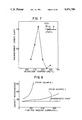
- FIG. 7 is a characteristic curve showing the discovered relationship between the deposition temperature and the encroachment length for tungsten.
- FIG. 8 shows characteristic curves of the contact resistance obtainable by the embodiments of the present invention.
- FIGS. 9(a) through (g) show cross sectional diagrams and a top view illustrating the process for a third embodiment of the present invention.
- FIGS. 10(a) through (g) show cross sectional diagrams illustrating the process for a fourth embodiment of the present invention.
- FIGS. 3(a) through 3(c) are the manufacturing process diagrams for a first embodiment of the present invention.
- an n + type diffused layer 12 with a junction depth of 0.15 ⁇ m is formed by ion implantation in a p-type Si substrate 11, then a silicon oxide film 13 with a thickness of 1 ⁇ m is deposited as an insulation film over the surface of the substrate by the Chemical Vapor Deposition (CVD) method, and a contact hole 14 for the diffused layer 12 is formed using the PEP process by selectively etching the oxide film 13.
- CVD Chemical Vapor Deposition
- a tungsten (W) layer 15 of thickness 200 angstroms is formed on the n + -type diffused layer 12 that is exposed to the contact hole 14, by means of the selective vapor phase growth method that employs tungsten hexafluoride (WF 6 ) and argon (Ar).
- the conditions for the selective growth in this case consist of a substrate temperature of 550 degrees Celsius, a pressure in the reaction furnace of 0.2 Torr, and a WF 6 partial pressure of 0.01 Torr. With these conditions, as the W film 15 grows, film 15 creeps up the sidewalls from the bottom of contact hole 14.
- an (Al) film is vacuum evaporated as an interconnection layer, interconnection 16 is formed by patterning the Al film. Finally, a heat treatment is given in a forming gas at 450 degrees Celsius for 15 minutes.
- the W film 15 serves as a protection against contact failure of the Al film, yet to damage occurs to the junction of diffused layer 12 and substrate 11 as a result of encroachment of W at the bottom portion of the contact hole along the interface between oxide film 13 and substrate 11.
- the lack of encroachment and the presence of "creep-up" the sidewall of contact hole 14 is a result of the conditions under which the W film 15 was formed.
- FIG. 4 is a cross section diagram showing a modification to the embodiment just described.
- the insulation film consists of a lamination of an SiO 2 film 13 obtained by CVD and a PSG film 13'. Since the W film 15 does not creep-up onto the surface of the PSG film 13', the amount of creeping up can be controlled in this embodiment.
- the extent of creeping up of the W film preferably is set to be more than 1/3 of the depth of the opening in the insulation film.
- FIGS. 5(a) to 5(c) are manufacturing process diagrams for a second embodiment of the present invention
- an n + -type diffusion layer 12 is formed on a p-type Si substrate 11, and oxide film 13 is deposited to a thickness of 1 on top of the layer 12 by the CVD method.
- a contact hole 14 for the oxide film 13 is formed.
- the process is similar to the first embodiment, shown in FIG. 3.
- a first W film 15 of thickness 200 angstroms is formed using WF 6 and Ar gases and formation conditions similar to the previous embodiment, so as not to create an encroachment of the W along the insulator to substrate interface.
- a thick W film 17 is buried on the inside of the contact hole 14 as shown in FIG.
- the growth conditions for thick W film 17 require a substrate temperature of 300 to 600 degrees Celsius, a pressure in the reaction furnace of 0.01 to 5 Torr, and a molar ratio of H 2 /WF 6 of 20. If the first growth process were omitted prior to the second growth process, the second W film may encroach along the insulator to substrate interface. Because a thin W film 15 is buried beforehand by the first growth process, (using conditions in which there will be no encroachment) the second film causes no device deterioration Additionally, the first W film on the sidewalls of the contact hole causes the second W film to grow from the sidewall area.
- an Al interconnection 16 is formed as shown in FIG. 5(c), similar to the first embodiment.
- electrical contacts can be made through extremely fine contact holes to underlying surface regions without accompanying breakdown of the surface regions to substrate junctions and, because the contact hole is buried with a thick W film in a two step growth process contact failures can be prevented resulting in improved reliability contacts.
- the thickness of the W film reaches a saturated value (saturated film thickness) which is a function of the deposition conditions.
- This saturated film thickness corresponds to the amount of W reduced with Si.
- the temperature dependence of the saturated W film thickness is shown in FIG. 6.
- the growth conditions for the W film were set at a pressure in the reaction furnace of 0.2 Torr and a WF 6 partial pressure of 0.01 Torr.
- FIG. 7 shows the discovered temperature dependence of the encroachment length D of the W film from the edge of the Si/Si0 2 interface. W film encroachment results in damage to the junction.
- the saturated thickness of the W film shows a maximum at 450 degrees Celsius and a minimum at 550 Celsius.
- the encroachment length D of the W film shows a at 450 degrees Celsius and decreases with increasing until, in the neighborhood of 550 degrees Celsius, growth of the W film occurs without creating encroachment. Instead, at about 550 degrees Celsius, the W film creeps-up on the sidewalls of the contact hole.
- Si reduction reaction of WF 6 may be represented by the following equation:
- the SiF 4 generated by this reaction attaches to the sidewalls of the contact hole, and the W film grows with the attached SiF.sub. 4 as the base. Consequently, the creep-up of the film is closely related to the amount of SiF 4 generated and the concentration of WF 6 .
- the particularly conspicuous creep-up of the W film resulting from the reduction reaction of WF 6 by the base Si occurs in the neighborhood of 550 degrees Celsius, where a minimum in the saturation of the deposited film thickness takes place.
- growth conditions may be selected from the substrate temperature range of 500 to 600 degrees Celsius, a pressure in the reaction furnace of more than 0.01 Torr (for example, 0.01 to 1 Torr), and a partial pressure of the halogenized high melting point metal of more than 0.001 Torr (for example, 0.001 to 0.5 Torr).
- WF 6 gas and Ar gasses were used in the above embodiments, but Ar may be replaced by other e gasses such as He, N 2 or H 2 may be used.
- a separate use of WF 6 may also be made, in which case the pressure in the reaction furnace should be over 0.001 Torr (for example, 0.001 to 0.5 Torr).
- FIG. 8 shows the results of stress tests (connection tests) on the contact resistance of the Al connection with the underlying diffused layer for the embodiments of the present invention
- the curve designated as EMBODIMENTS 1 AND 2 corresponds to the embodiments shown in FIGS. 3, 4, and 5
- the curve marked as PRIOR EXAMPLE 1 corresponds to the case of direct contact with the A1 interconnection (A1+1% Si) without growing a W film for the n + -type diffused layer.
- the curve marker as PRIOR EXAMPLE 2 is for a process which is basically similar to the embodiment shown in FIG. 3.
- the substrate temperature for the selective growth of the W film was set at a low temperature of 350 degrees Celsius and a W film with a thickness 200 angstroms was grown Only in the bottom section of the contact hole.
- the interconnection according to the present invention shows no increase in the contact resistance, even for a stress test of 600 hours, and shows a marked improvement in reliability.
- the present invention is by no means limited to the above embodiment.
- the method and resultant apparatus of the present invention may also be applied where an interconnection is made via a contact hole to a surface of a semiconductor device in the form of an electrode of polycrystalline Si film formed on an oxide film with doping of lead, boron, or arsenic.
- the problem of contact failure still exists in such a case because of a volume contraction in the encroachment section that creates gaps in the insulation film, lowering the reliability of the contact.
- the embodiments shown in FIGS. 3 and 4 have only one process of W film growth, while the embodiment shown in FIG. 5 has two stages of growth.
- the present invention is effective so long as the growth conditions are set to have the film creep-up the sidewalls of the contact hole.
- the second embodiment used selective growth of a second W film.
- the present invention can still further be applied to the growth of films of other high melting point metals such as molybdenum (Mo) tantalum (Ta), and titanium (Ti) by means of similar vapor phase growth methods using MoF 6 , TaF 6 , TiF 6 and so on.
- Mo molybdenum
- TaF 6 tantalum
- Ti titanium
- FIGS. 9(a) through 9(f) illustrate the manufacturing process of a MOSFET device according to a third embodiment of the present invention.
- a field oxide film (insulation film) 22 for separation of elements is formed on a p-type silicon substrate 21 to obtain an element formation region.
- a gate electrode 24 that consists of a polycrystalline silicon layer heavily doped with phosphorus.
- shallow n -1 diffused layers 25a and 25b are formed to establish source and drain regions by implanting phosphorus ions (P + ) by means of the ion implantation method with an accelerating voltage of 40 KeV and an implantation amount of 1 ⁇ 10 14 /cm 2 , using the gate electrode 24 and the field oxide film 22 as a mask as shown in FIG. 9(a).
- oxidation of hydrogen by combustion is carried out by heating the system to a temperature of 750 degrees Celsius to form an oxide film (insulation film) 26 over the surface of the shallow diffused layer for the gate electrode 24 and the source and drain regions.
- oxide film insulation film
- the thickness of the oxide film was 600 angstroms over the gate electrode while it was 100 angstroms over the source and drain regions.
- the oxide film 26 is etched until the source and drain regions are exposed by reactive ion etching which makes use of a freon series gas or by wet etching which makes use of a diluted solution of fluoric acid.
- reactive ion etching which makes use of a freon series gas
- wet etching which makes use of a diluted solution of fluoric acid.
- deep n + diffused layers 27a and 27b are formed in the source and drain regions by implanting arsenic ions by the ion implantation method with an accelerating voltage of 50 KeV and an implantation amount of 1 ⁇ 10 16 /cm 2 .
- W films 28 are grown selectively the deep n + diffused layers 27a and 27b and over the neighboring insulation films 22 and 26 so as to creep-up these films by the CVD method at low pressure.
- the low pressure CVD process for the W film formation consists of two processes.
- the first process is for formation of a thin W film with thickness of about 200 angstroms over the n + diffused layers 27a and 27b and over the surrounding insulation films 22 and 26 by using WF 6 and Ar gasses with the following conditions: a substrate temperature of 550 degrees Celsius , a vacuum of 0.2 Torr, WF 6 partial pressure of 0.01 Torr, and a deposition time of 3 minutes.
- the second process is one for increasing the thickness of the thin W film obtained by the first process to a predetermined thickness, using WF 6 and H 2 as the reaction gases (keeping the molar ratio of H 2 /WF 6 to 20 ) under the conditions of a substrate temperature of 300 to 600 degrees Celsius and a pressure in the reaction furnace of 0.01 to 5 Torr.
- the W film 28 extends over the insulation films 22 and 26 that are situated in the neighborhood of the n + diffused layers 27a and 27b.
- an insulation film 29 consisting of silicon oxide (SiO 2 ) is deposited by the plasma CVD method using silane (SiH 4 ) and nitrogen oxide (N 2 O) gasses. Then, contact holes 30a, 30b, and 30c are created by the reactive ion etching method that makes use of a freon series gas, with a resist pattern (not shown) that is formed by the photoetching method as a mask. Now, the oxide film formed is thicker on the gate electrode than on the source and drain regions (n + diffused layers 27a and 27b).
- FIG. 9(e) corresponds to the A-A cross section of FIG. 9(f).
- an Al film with a thickness of 0.8 ⁇ m is deposited on top of the surface as shown in FIG. 9(g) by the sputtering method.
- the interconnections 31a and 31b for the source and drain regions and an interconnection for the gate (not shown) are formed by patterning the Al film.
- a MOSFET formed in this manner has high reliability contacts with low electrical resistance, since a W film is interposed extending from the shallow diffused source and drain regions to the surface of the gate. Further, the W film can prevent overetching in the formation of contact holes in the field oxide film, generated as a result of overetching and mismatching in the source and drain regions, even when the overetching and mismatching cover a part of the field. Therefore, even with extreme miniaturization of the elements, junction breakdowns can be avoided, resulting in highly reliable electrical contacts.
- an element formation region is obtained by forming a field oxide film 42 for element separation on a p-type silicon substrate.
- a gate oxide film 43, polycrystalline silicon film 44 which is heavily doped with phosphorus, and insulation film 45 consisting of a silicon oxide film formed by the CVD method are formed in succession over the field oxide film 42.
- the silicon oxide film 45 is patterned as shown in FIG. 10(b) by means of the photolithography method.
- a gate electrode 44 is formed by selectively removing the gate oxide film 43 and the polycrystalline silicon film 44 by reactive ion etching which makes use of a freon series gas, with the silicon oxide film 45 as the mask.
- shallow n - diffused layers 46a and 46b are formed in the source and drain regions by implanting phosphorus ions by means of the ion implantation method, using an accelerating voltage of 40 KeV and an implantation amount of 1 ⁇ 10 4 /cm 2 , as shown in FIG. 10(c).
- an insulation film 47 consisting of a silicon oxide film with thickness of 0.3 ⁇ m is deposited over the surface of the substrate by the CVD method. Then, the surface is etched by means of the reactive ion etching method by making use of a freon series gas, leaving the insulation films 45 and 47 to cover the gate electrode.
- etching proceeds in the vertical direction alone so that the insulation film 47 remains on the sidewalls of the gate electrode 44.
- the insulation film 47 is laminated over the insulation film 45 that was formed in the preceding process so that the insulation film 45 remains after the insulation film 47 on the source and drain regions is removed.
- n + diffused layers 48a and 48b are formed deep in the source and drain regions by implanting arsenic ions (As 30 ) by the ion implanting method as shown in FIG. 10(e) with an accelerating voltage of 50 KeV and an implantation amount of 1 ⁇ 10 16 /cm 2 .
- a W film 49 is grown selectively by the low pressure CVD method over the deep n + diffused layers 48a and 48b in the source and drain regions and over the neighboring insulation films 42, 47, and 45 to creep-up on these films.
- an insulation film 50 consisting of silicon oxide film is deposited over the surface by the plasma CVD method to form contact holes 51a and 51b that are created by the reactive ion etching, FIG. 10(f).
- the contact holes are arranged to be formed toward the outside, namely toward the field oxide film, from the source and drain regions.
- the W film 49 acts again as an etching stopper so that no etching will occur in the n + diffused layers 48a and 48b and the field oxide film 42.
- an interconnection layer consisting of Al film is formed by the sputtering method, and the interconnections 52a and 52b and the interconnection for the gate (not shown) are formed by sputtering.
- the formation process of the insulation film for covering the gate electrode differs from that in the preceding embodiment. Contacts formed in this manner have an extremely high reliability as in the preceding embodiment. Also, in this embodiment, a W film is selectively formed over the source and drain regions and over the insulation film surrounding it. Other high melting point metals such as Mo, Ta, and Ti may be used.
Abstract
Contact with a substrate or conductor underlying an opening in the insulating layer is made by depositing a thin film of high melting point metal using a selective vapor phase growth process so that the metal film grows across the exposed surface and then creeps-up the sidewalls of the insulating layer. Electrical contact is completed by covering the thin film with a thicker growth of high melting point metal, preferably using a second selective vapor phase growth process, and then depositing a conducting film over the insulating layer in electrical contact with the thicker growth of metal.
Description
This application is a continuation of application Ser. No. 07/425,455, filed Oct. 23, 1989, now abandoned, which is a continuation of application Ser. No. 07/178,255, filed Apr. 5, 1988, now abandoned, which is a continuation of application Ser. No. 06/890,920, filed July 30, 1986, now abandoned.
1. Field of the Invention
The present invention relates to electrical connections for a semiconductor device made from high melting point metal and to related methods of making these connections to assure good electrical contact between interconnected semiconductor device elements.
2. Background Information
As the degree of integration of MOS integrated circuit elements increases, the area available for making electrical connections between metallic conductors and semiconductor surface regions, such as polycrystalline-silicon gate electrodes or source-drain diffused layers, is becoming extremely small. Moreover, the depth of pn junctions in surface diffused layers is becoming extremely shallow. The sputtering method, which ordinarily is used for making electrical connections to such regions, tends to produce deteriorated connections as the size of contact holes through overlying insulating layers becomes increasingly small. Frequently, metallic conductors fail to contact the surface region region at the bottom of the contact hole because of a "shadowing" effect, shown in FIG. 1, where metal deposition at the top of the sidewalls of the contact hole prevents sufficient deposition of metal at the bottom of the hole to achieve a good electrical connection with the underlying surface region. In giant LSI circuits having more than one million elements on a several millimeter square chip, such a deterioration in the electrical connections results in a substantial reduction in the reliability of the resultant device.
Growth of thin films of tungsten at the bottom of the contact hole to facilitate connection with overlying conductors may result in tungsten encroachment along the edges of the interface of the insulation layer in which the contact hole is made and the surface region to which electrical contact is to be made, resulting in degradation of device performance. This encroachment was thought to increase with temperature and partial pressure as shown in FIG. 2.
In current day 64K bit 256K bit dynamic random access MOS-type memories, the for mask matching is on the order of 0.2 μm, or less than . of the minimum size of 2 to 3 μm for a memory element. minimum size becomes 1 μm or enters the submicron region matching precisions of less than 0.1 μm will be necessary. However, since the matching precision is largely dictated b mechanical precision of the semiconductor device, a precision of 0.1 μm will be difficult to achieve and will result in the following problems. First, contact hole mismatches will . in a decrease of the contact area between aluminum i ion material and the underlying surface regions to which elect contact is to be made, causing increased electrical resistance. Second, overetching during preparation of the hole will cause defects such as punctures in the interconnect areas because of the decrease in the area of the insulation film in the region surrounding the underlying source and drain regions, and will result in defective connections.
Accordingly, there exists a need for a technique to produce highly reliable electrical connections that do not significantly deteriorate the performance of semiconductor devices.
It is, accordingly, an object of the present invention to provide high reliability electrical connections and methods of forming same.
Additional objects and advantages of the invention will be set forth in the description which follows, and in part will be obvious from the description, or may be learned by practice of the invention.
To achieve the foregoing objects, and in accordance with the purposes of the invention as embodied and broadly described herein, a method of forming an electrical connection to a surface of a semiconductor device adjacent a sidewall of insulating material, is provided, comprising the steps of: (a) exposing the surface to a halogenized gas of a high melting point metal under conditions to reduce the gas with the surface to result in formation of a layer of the metal on the surface, the conditions including deposition of the layer at a sufficiently high temperature to essentially minimize the resultant thickness of the layer, whereby the layer is also formed extending up the sidewall; and (b) forming a conductor in electrical contact with the layer to thereby form electrical connection with the surface.
Additionally, an electrical connection to a surface of a semiconductor device adjacent a sidewall of insulating material, is provided, comprising: (a) a thin film of a high melting point metal formed on the surface by vapor deposition and formed on a portion of the sidewall by creeping of the metal up onto the portion of the sidewall from the portion of the metal formed on the surface; and (b) a conductor formed in electrical contact with the thin film thereby forming electrical connection with the surface.
FIG. 1 shows a cross sectional diagram illustrating the drawbacks of the prior art.
FIG. 2 shows a prior art characteristic curve of the relationship of encroachment depth with temperature.
FIGS. 3(a) through 3(c) show cross sectional diagrams for illustrating the process for a first embodiment of the present invention.
FIG. 4 is a cross sectional diagram illustrating a modification to the device shown in FIGS. 3(a) through 3(c).
FIGS. 5(a) through 5(c) show cross sectional diagrams illustrating the process for a second embodiment of the present invention.
FIG. 6 is a characteristic curve showing the discovered relationship between the deposition temperature and the saturated film thickness for tungsten.
FIG. 7 is a characteristic curve showing the discovered relationship between the deposition temperature and the encroachment length for tungsten.
FIG. 8 shows characteristic curves of the contact resistance obtainable by the embodiments of the present invention.
FIGS. 9(a) through (g) show cross sectional diagrams and a top view illustrating the process for a third embodiment of the present invention.
FIGS. 10(a) through (g) show cross sectional diagrams illustrating the process for a fourth embodiment of the present invention.
FIGS. 3(a) through 3(c) are the manufacturing process diagrams for a first embodiment of the present invention. As shown in FIG. 3(a), an n+ type diffused layer 12 with a junction depth of 0.15 μm is formed by ion implantation in a p-type Si substrate 11, then a silicon oxide film 13 with a thickness of 1 μm is deposited as an insulation film over the surface of the substrate by the Chemical Vapor Deposition (CVD) method, and a contact hole 14 for the diffused layer 12 is formed using the PEP process by selectively etching the oxide film 13. Then as shown :n FIG. 3(b), a tungsten (W) layer 15 of thickness 200 angstroms is formed on the n+ -type diffused layer 12 that is exposed to the contact hole 14, by means of the selective vapor phase growth method that employs tungsten hexafluoride (WF6) and argon (Ar). The conditions for the selective growth in this case consist of a substrate temperature of 550 degrees Celsius, a pressure in the reaction furnace of 0.2 Torr, and a WF6 partial pressure of 0.01 Torr. With these conditions, as the W film 15 grows, film 15 creeps up the sidewalls from the bottom of contact hole 14. After that, as shown in FIG. 3(c), an (Al) film is vacuum evaporated as an interconnection layer, interconnection 16 is formed by patterning the Al film. Finally, a heat treatment is given in a forming gas at 450 degrees Celsius for 15 minutes.
According to this embodiment, it is possible to obtain satisfactory electrical connection with a surface region exemplified by diffusion layer 12, since the W film 15 serves as a protection against contact failure of the Al film, yet to damage occurs to the junction of diffused layer 12 and substrate 11 as a result of encroachment of W at the bottom portion of the contact hole along the interface between oxide film 13 and substrate 11. As will be explained in more detail below, the lack of encroachment and the presence of "creep-up" the sidewall of contact hole 14 is a result of the conditions under which the W film 15 was formed.
FIG. 4 is a cross section diagram showing a modification to the embodiment just described. Here, the insulation film consists of a lamination of an SiO2 film 13 obtained by CVD and a PSG film 13'. Since the W film 15 does not creep-up onto the surface of the PSG film 13', the amount of creeping up can be controlled in this embodiment.
In the embodiments shown in FIGS. 3 and 4, to prevent the Al film 16 from failing to make adequate contact, the extent of creeping up of the W film preferably is set to be more than 1/3 of the depth of the opening in the insulation film.
FIGS. 5(a) to 5(c) are manufacturing process diagrams for a second embodiment of the present invention As shown in FIG. 5(a), an n+ -type diffusion layer 12 is formed on a p-type Si substrate 11, and oxide film 13 is deposited to a thickness of 1 on top of the layer 12 by the CVD method. A contact hole 14 for the oxide film 13 is formed. Up to this point, the process is similar to the first embodiment, shown in FIG. 3. A first W film 15 of thickness 200 angstroms is formed using WF6 and Ar gases and formation conditions similar to the previous embodiment, so as not to create an encroachment of the W along the insulator to substrate interface. Next, a thick W film 17 is buried on the inside of the contact hole 14 as shown in FIG. 5(b) by a second growth process using WF6 and H2 gases. The growth conditions for thick W film 17 require a substrate temperature of 300 to 600 degrees Celsius, a pressure in the reaction furnace of 0.01 to 5 Torr, and a molar ratio of H2 /WF6 of 20. If the first growth process were omitted prior to the second growth process, the second W film may encroach along the insulator to substrate interface. Because a thin W film 15 is buried beforehand by the first growth process, (using conditions in which there will be no encroachment) the second film causes no device deterioration Additionally, the first W film on the sidewalls of the contact hole causes the second W film to grow from the sidewall area. Therefore, the time for growing the second W film is short, and sufficient selectivity for deposition of the film over the flat surface of the oxide film 13 can be retained. In cases where selectivity cannot be maintained, a W film might also form on the flat oxide film, causing device failures. In the next step, an Al interconnection 16 is formed as shown in FIG. 5(c), similar to the first embodiment.
In this second embodiment, electrical contacts can be made through extremely fine contact holes to underlying surface regions without accompanying breakdown of the surface regions to substrate junctions and, because the contact hole is buried with a thick W film in a two step growth process contact failures can be prevented resulting in improved reliability contacts.
The following discussion presents the reasons why a W film grown according to the methods taught by this invention does not grown according to the methods taught by this invention does not encroach along the interface between the insulation film and the substrate, according to theories based on currently available experimental data.
In the silicon reduction reaction of WF6, the thickness of the W film reaches a saturated value (saturated film thickness) which is a function of the deposition conditions. This saturated film thickness corresponds to the amount of W reduced with Si. The temperature dependence of the saturated W film thickness is shown in FIG. 6. In this case, the growth conditions for the W film were set at a pressure in the reaction furnace of 0.2 Torr and a WF6 partial pressure of 0.01 Torr. FIG. 7 shows the discovered temperature dependence of the encroachment length D of the W film from the edge of the Si/Si02 interface. W film encroachment results in damage to the junction. According to experimental results, the saturated thickness of the W film shows a maximum at 450 degrees Celsius and a minimum at 550 Celsius. The encroachment length D of the W film shows a at 450 degrees Celsius and decreases with increasing until, in the neighborhood of 550 degrees Celsius, growth of the W film occurs without creating encroachment. Instead, at about 550 degrees Celsius, the W film creeps-up on the sidewalls of the contact hole.
Although the mechanism for a decrease in the encroachment with an increase in temperature beyond 450 degrees Celsius is not clear yet, this discovery may be explained as follows. The Si reduction reaction of WF6 may be represented by the following equation:
WF.sub.6 (g)+(3/2)Si(s)→W(s)+(3/2)SiF.sub.4 (g)
The SiF4 generated by this reaction attaches to the sidewalls of the contact hole, and the W film grows with the attached SiF.sub. 4 as the base. Consequently, the creep-up of the film is closely related to the amount of SiF4 generated and the concentration of WF6. The particularly conspicuous creep-up of the W film resulting from the reduction reaction of WF6 by the base Si occurs in the neighborhood of 550 degrees Celsius, where a minimum in the saturation of the deposited film thickness takes place.
At 550 degrees Celsius, the amount of creep-up of W film shown in FIG. 3 and FIG. 9 (to be described water), far exceeded ten times the saturated film thickness D. Even at 550 ±30 degrees Celsius, the value of L/D was greater than 3. Thus it is important to grow the W film at its minimum thickness in order to bring about a conspicuous creep-up, suppress encroachment, and obtain a high reliability contact.
Although the W film was grown at 550 degrees Celsius under the above conditions, growth conditions may be selected from the substrate temperature range of 500 to 600 degrees Celsius, a pressure in the reaction furnace of more than 0.01 Torr (for example, 0.01 to 1 Torr), and a partial pressure of the halogenized high melting point metal of more than 0.001 Torr (for example, 0.001 to 0.5 Torr). WF6 gas and Ar gasses were used in the above embodiments, but Ar may be replaced by other e gasses such as He, N2 or H2 may be used. A separate use of WF6 may also be made, in which case the pressure in the reaction furnace should be over 0.001 Torr (for example, 0.001 to 0.5 Torr).
FIG. 8 shows the results of stress tests (connection tests) on the contact resistance of the Al connection with the underlying diffused layer for the embodiments of the present invention The curve designated as EMBODIMENTS 1 AND 2 corresponds to the embodiments shown in FIGS. 3, 4, and 5 The curve marked as PRIOR EXAMPLE 1 corresponds to the case of direct contact with the A1 interconnection (A1+1% Si) without growing a W film for the n+ -type diffused layer. The curve marker as PRIOR EXAMPLE 2 is for a process which is basically similar to the embodiment shown in FIG. 3. However, the substrate temperature for the selective growth of the W film was set at a low temperature of 350 degrees Celsius and a W film with a thickness 200 angstroms was grown Only in the bottom section of the contact hole. As may be clear from these experimental findings, the interconnection according to the present invention shows no increase in the contact resistance, even for a stress test of 600 hours, and shows a marked improvement in reliability.
The present invention is by no means limited to the above embodiment. Thus, for example, in the embodiments described, reference was made where an interconnection is made to a surface of a semiconductor device in the form of a diffused layer in the surface of a Si substrate. However, the method and resultant apparatus of the present invention may also be applied where an interconnection is made via a contact hole to a surface of a semiconductor device in the form of an electrode of polycrystalline Si film formed on an oxide film with doping of lead, boron, or arsenic. The problem of contact failure still exists in such a case because of a volume contraction in the encroachment section that creates gaps in the insulation film, lowering the reliability of the contact.
The embodiments shown in FIGS. 3 and 4 have only one process of W film growth, while the embodiment shown in FIG. 5 has two stages of growth. The present invention is effective so long as the growth conditions are set to have the film creep-up the sidewalls of the contact hole. Also, the second embodiment used selective growth of a second W film. The present invention can still further be applied to the growth of films of other high melting point metals such as molybdenum (Mo) tantalum (Ta), and titanium (Ti) by means of similar vapor phase growth methods using MoF6, TaF6, TiF6 and so on.
FIGS. 9(a) through 9(f) illustrate the manufacturing process of a MOSFET device according to a third embodiment of the present invention.
First, a field oxide film (insulation film) 22 for separation of elements is formed on a p-type silicon substrate 21 to obtain an element formation region. Then, on a thin gate oxide film 23 formed in the element formation region, there is formed a gate electrode 24 that consists of a polycrystalline silicon layer heavily doped with phosphorus. Subsequently, shallow n-1 diffused layers 25a and 25b are formed to establish source and drain regions by implanting phosphorus ions (P+) by means of the ion implantation method with an accelerating voltage of 40 KeV and an implantation amount of 1×10¹⁴ /cm2, using the gate electrode 24 and the field oxide film 22 as a mask as shown in FIG. 9(a).
Next as shown in FIG. 9(b), oxidation of hydrogen by combustion is carried out by heating the system to a temperature of 750 degrees Celsius to form an oxide film (insulation film) 26 over the surface of the shallow diffused layer for the gate electrode 24 and the source and drain regions. In so doing, it is possible to enhance the dependence of the oxidation speed on the impurity concentration by carrying out the hydrogen oxidation by combustion at a low temperature of 750 degrees Celsius to form a thicker oxide film over the gate electrode than over the source and drain regions. The thickness of the oxide film was 600 angstroms over the gate electrode while it was 100 angstroms over the source and drain regions.
Subsequently, as shown in FIG. 9(c), the oxide film 26 is etched until the source and drain regions are exposed by reactive ion etching which makes use of a freon series gas or by wet etching which makes use of a diluted solution of fluoric acid. Following that, deep n+ diffused layers 27a and 27b are formed in the source and drain regions by implanting arsenic ions by the ion implantation method with an accelerating voltage of 50 KeV and an implantation amount of 1×10¹⁶ /cm2.
Next, as shown in FIG. 9(d), W films 28 are grown selectively the deep n+ diffused layers 27a and 27b and over the neighboring insulation films 22 and 26 so as to creep-up these films by the CVD method at low pressure.
Here, the low pressure CVD process for the W film formation consists of two processes. The first process is for formation of a thin W film with thickness of about 200 angstroms over the n+ diffused layers 27a and 27b and over the surrounding insulation films 22 and 26 by using WF6 and Ar gasses with the following conditions: a substrate temperature of 550 degrees Celsius , a vacuum of 0.2 Torr, WF6 partial pressure of 0.01 Torr, and a deposition time of 3 minutes. The second process is one for increasing the thickness of the thin W film obtained by the first process to a predetermined thickness, using WF6 and H2 as the reaction gases (keeping the molar ratio of H2 /WF6 to 20 ) under the conditions of a substrate temperature of 300 to 600 degrees Celsius and a pressure in the reaction furnace of 0.01 to 5 Torr. As a result, the W film 28 extends over the insulation films 22 and 26 that are situated in the neighborhood of the n+ diffused layers 27a and 27b.
Further, as shown in FIGS. 9(e) and 9(f), an insulation film 29 consisting of silicon oxide (SiO2) is deposited by the plasma CVD method using silane (SiH4) and nitrogen oxide (N2 O) gasses. Then, contact holes 30a, 30b, and 30c are created by the reactive ion etching method that makes use of a freon series gas, with a resist pattern (not shown) that is formed by the photoetching method as a mask. Now, the oxide film formed is thicker on the gate electrode than on the source and drain regions (n+ diffused layers 27a and 27b). In contrast to the overetching of the source and drain regions that occurs in the ordinary process, in the present process where a W film acts as an etching stopper, no etching will take place for the n+ diffused layers 27a and 27b and for the insulation film 26 on the sidewalls of the gate electrode. FIG. 9(e) corresponds to the A-A cross section of FIG. 9(f).
Next, an Al film with a thickness of 0.8 μm is deposited on top of the surface as shown in FIG. 9(g) by the sputtering method. The interconnections 31a and 31b for the source and drain regions and an interconnection for the gate (not shown) are formed by patterning the Al film.
A MOSFET formed in this manner has high reliability contacts with low electrical resistance, since a W film is interposed extending from the shallow diffused source and drain regions to the surface of the gate. Further, the W film can prevent overetching in the formation of contact holes in the field oxide film, generated as a result of overetching and mismatching in the source and drain regions, even when the overetching and mismatching cover a part of the field. Therefore, even with extreme miniaturization of the elements, junction breakdowns can be avoided, resulting in highly reliable electrical contacts.
The manufacturing process of MOSFET devices according to a fourth embodiment of the present invention will now be described. First, as shown in FIG. 10(a), an element formation region is obtained by forming a field oxide film 42 for element separation on a p-type silicon substrate. Then, a gate oxide film 43, polycrystalline silicon film 44 which is heavily doped with phosphorus, and insulation film 45 consisting of a silicon oxide film formed by the CVD method, are formed in succession over the field oxide film 42. Next, the silicon oxide film 45 is patterned as shown in FIG. 10(b) by means of the photolithography method. Then, a gate electrode 44 is formed by selectively removing the gate oxide film 43 and the polycrystalline silicon film 44 by reactive ion etching which makes use of a freon series gas, with the silicon oxide film 45 as the mask.
After that, shallow n- diffused layers 46a and 46b are formed in the source and drain regions by implanting phosphorus ions by means of the ion implantation method, using an accelerating voltage of 40 KeV and an implantation amount of 1×10⁴ /cm2, as shown in FIG. 10(c). Further, as shown in FIG. 10(d), an insulation film 47 consisting of a silicon oxide film with thickness of 0.3 μm is deposited over the surface of the substrate by the CVD method. Then, the surface is etched by means of the reactive ion etching method by making use of a freon series gas, leaving the insulation films 45 and 47 to cover the gate electrode. In the reactive ion etching method, etching proceeds in the vertical direction alone so that the insulation film 47 remains on the sidewalls of the gate electrode 44. On the other hand, the insulation film 47 is laminated over the insulation film 45 that was formed in the preceding process so that the insulation film 45 remains after the insulation film 47 on the source and drain regions is removed.
In this way, n+ diffused layers 48a and 48b are formed deep in the source and drain regions by implanting arsenic ions (As30 ) by the ion implanting method as shown in FIG. 10(e) with an accelerating voltage of 50 KeV and an implantation amount of 1×10¹⁶ /cm2.
Thereafter, the process is similar to that applied to the preceding embodiment. First, a W film 49 is grown selectively by the low pressure CVD method over the deep n+ diffused layers 48a and 48b in the source and drain regions and over the neighboring insulation films 42, 47, and 45 to creep-up on these films. Then, an insulation film 50 consisting of silicon oxide film is deposited over the surface by the plasma CVD method to form contact holes 51a and 51b that are created by the reactive ion etching, FIG. 10(f). Here, the contact holes are arranged to be formed toward the outside, namely toward the field oxide film, from the source and drain regions. In this case, the W film 49 acts again as an etching stopper so that no etching will occur in the n+ diffused layers 48a and 48b and the field oxide film 42.
After that, an interconnection layer consisting of Al film is formed by the sputtering method, and the interconnections 52a and 52b and the interconnection for the gate (not shown) are formed by sputtering.
In the present process, the formation process of the insulation film for covering the gate electrode differs from that in the preceding embodiment. Contacts formed in this manner have an extremely high reliability as in the preceding embodiment. Also, in this embodiment, a W film is selectively formed over the source and drain regions and over the insulation film surrounding it. Other high melting point metals such as Mo, Ta, and Ti may be used.
Additional advantages and modifications will readily occur to those skilled in the art. The invention in its broader aspects is therefore not limited to the specific details, representative steps, and illustrative examples shown and described. Accordingly, departures may be made from such details without departing from the spirit or scope of the applicant's general inventive concept.
Claims (14)
1. A method of forming an electrical connection to a silicon surface of a semiconductor device adjacent a sidewall of insulating material comprising the steps of:
a. exposing said surface to a halogenated gas of a metal with a high melting point under conditions to reduce said gas with said silicon to result in formation of a layer of said metal having a saturated thickness on said surface, said conditions being selected such that: (i) the saturated thickness of said layer is dependent upon the temperature od depostion, (ii) the saturated thickness of said layer increases with a higher temperature of deposition until an initial maximum thickness is obtainable at a first temperature of deposition and (iii) the saturated thickness of said layer decreases from said initial maximum thickness as the temperature increases from said first temperature of deposition until a second temperature is reached at which a minimized thickness is obtainable, said conditions including deposition of said layer at said second temperature to essentially minimize the saturated thickness of said layer, with said layer also being formed extending up said sidewall; and
b. forming a conductor in electrical contact with said layer to thereby form electrical connection with said surface.
2. A method of claim 1 wherein said gas used in said step of exposing is WF6, MoF6, TaF6, or TiF6.
3. A method of claim 2 wherein said conditions include exposing said surface to a rare gas.
4. A method of claim 3 wherein said rare gas is Ar or He.
5. A method of claim 2 wherein said conditions include exposing said surface to N2 gas.
6. A method of claim 1 wherein said high temperature is set ±30 degrees Celsius of said second temperature.
7. A method of claim 1 wherein said second temperature is 550 degrees Celsius.
8. A method of claim 7 wherein said conditions further include a reactor of 0.2 Torr and a partial pressure for said halogenated gas of 0.01 Torr.
9. A method of claim 8 wherein said halogenated gas is WF6.
10. A method of claims 1, 2, 3, 4, 5, 6, 7, 8, or 9 wherein said step of exposing is continued until said metal extends up said sidewall a distance greater than three times the thickness of said layer.
11. A method of claim 10 wherein said step of exposing is continued until said metal extends up said sidewall a distance greater than ten times the thickness of said layer.
12. A method of claims 1, 2, 3, 4, 5, 6, 7, 8, or 9 wherein said insulating layer is SiO2.
13. A method of claim 1 further comprising the steps of:
c. exposing said layer of said metal to a mixture gas of said halogenated gas of a metal and a hydrogen gas to form an additional metal layer on said layer,
wherein said step c is performed between said steps a and b, and said layer of said step a is obtained substantially only by the reducing of said halogenated gas with said silicon.
14. A method of claim 13 wherein said step c is performed until a contact hole which comprises said sidewall of said insulating material is buried with said additional metal layer.
Applications Claiming Priority (2)
| Application Number | Priority Date | Filing Date | Title |
|---|---|---|---|
| JP60170764A JPS6231116A (en) | 1985-08-02 | 1985-08-02 | Manufacture of semiconductor device |
| JP60-170764 | 1985-08-02 |
Related Parent Applications (1)
| Application Number | Title | Priority Date | Filing Date |
|---|---|---|---|
| US07425455 Continuation | 1989-10-23 |
Publications (1)
| Publication Number | Publication Date |
|---|---|
| US5071789A true US5071789A (en) | 1991-12-10 |
Family
ID=15910942
Family Applications (1)
| Application Number | Title | Priority Date | Filing Date |
|---|---|---|---|
| US07/536,933 Expired - Lifetime US5071789A (en) | 1985-08-02 | 1990-06-12 | Method for forming a metal electrical connector to a surface of a semiconductor device adjacent a sidewall of insulation material with metal creep-up extending up that sidewall, and related device |
Country Status (4)
| Country | Link |
|---|---|
| US (1) | US5071789A (en) |
| JP (1) | JPS6231116A (en) |
| KR (1) | KR900001654B1 (en) |
| DE (1) | DE3625860A1 (en) |
Cited By (12)
| Publication number | Priority date | Publication date | Assignee | Title |
|---|---|---|---|---|
| US5202287A (en) * | 1989-01-06 | 1993-04-13 | International Business Machines Corporation | Method for a two step selective deposition of refractory metals utilizing SiH4 reduction and H2 reduction |
| US5227336A (en) * | 1991-12-27 | 1993-07-13 | Small Power Communication Systems Research Laboratories Co., Ltd. | Tungsten chemical vapor deposition method |
| US5246879A (en) * | 1990-09-28 | 1993-09-21 | The United States Of America As Represented By The Secretary Of The Navy | Method of forming nanometer-scale trenches and holes |
| DE4417966A1 (en) * | 1994-05-21 | 1995-11-23 | Fraunhofer Ges Forschung | Modular contacting process for multilayer device |
| US5470789A (en) * | 1993-03-19 | 1995-11-28 | Fujitsu Limited | Process for fabricating integrated circuit devices |
| US5484747A (en) * | 1995-05-25 | 1996-01-16 | United Microelectronics Corporation | Selective metal wiring and plug process |
| US5683938A (en) * | 1991-10-21 | 1997-11-04 | Hyundai Electronics Industries Co., Ltd. | Method for filling contact holes with metal by two-step deposition |
| US6013575A (en) * | 1995-07-07 | 2000-01-11 | Kabushiki Kaisha Toshiba | Method of selectively depositing a metal film |
| USRE36663E (en) * | 1987-12-28 | 2000-04-18 | Texas Instruments Incorporated | Planarized selective tungsten metallization system |
| US6180513B1 (en) * | 1996-08-13 | 2001-01-30 | Kabushiki Kaisha Toshiba | Apparatus and method for manufacturing a semiconductor device having a multi-wiring layer structure |
| US6204561B1 (en) * | 1995-11-10 | 2001-03-20 | Nippon Steel Corporation | Semiconductor device having two-layer contact |
| US20080056946A1 (en) * | 2003-04-28 | 2008-03-06 | Lubna Ahmad | Thermoelectric sensor for analytes in a fluid and related method |
Families Citing this family (6)
| Publication number | Priority date | Publication date | Assignee | Title |
|---|---|---|---|---|
| JPS5643310A (en) * | 1979-09-19 | 1981-04-22 | Sumitomo Naugatuck Co Ltd | Production of copolymer latex |
| EP0319214A1 (en) * | 1987-12-04 | 1989-06-07 | AT&T Corp. | Method for making semiconductor integrated circuits using selective tungsten deposition |
| FR2624304B1 (en) * | 1987-12-04 | 1990-05-04 | Philips Nv | METHOD FOR ESTABLISHING AN ELECTRICAL INTERCONNECTION STRUCTURE ON A SILICON SEMICONDUCTOR DEVICE |
| EP0326956A3 (en) * | 1988-02-02 | 1991-03-13 | National Semiconductor Corporation | Method for connecting devices on an integrated circuit substrate to a metallization layer |
| FR2630587A1 (en) * | 1988-04-22 | 1989-10-27 | Philips Nv | METHOD FOR ESTABLISHING SMALL-SIZE ELECTRIC CONTACTS ON A SEMICONDUCTOR DEVICE |
| JPH01298765A (en) * | 1988-05-27 | 1989-12-01 | Fujitsu Ltd | Semiconductor device and manufacture thereof |
Citations (9)
| Publication number | Priority date | Publication date | Assignee | Title |
|---|---|---|---|---|
| US4271424A (en) * | 1977-06-09 | 1981-06-02 | Fujitsu Limited | Electrical contact connected with a semiconductor region which is short circuited with the substrate through said region |
| JPS5928360A (en) * | 1982-08-10 | 1984-02-15 | Nec Corp | Manufacture of semiconductor device |
| JPS5961446A (en) * | 1982-09-30 | 1984-04-07 | Toshiba Corp | Electromagnetic damper shield of superconductive rotor and manufacture thereof |
| JPS5963745A (en) * | 1983-06-06 | 1984-04-11 | Nec Corp | Semiconductor device |
| JPS5984576A (en) * | 1982-11-08 | 1984-05-16 | Nec Corp | Manufacture of semiconductor device |
| JPS60186038A (en) * | 1984-03-05 | 1985-09-21 | Fujitsu Ltd | Semiconductor device |
| JPS60229350A (en) * | 1984-04-27 | 1985-11-14 | Toshiba Corp | Manufacture of semiconductor device |
| US4616401A (en) * | 1984-06-19 | 1986-10-14 | Kabushiki Kaisha Toshiba | Method of fabricating an insulated gate type field-effect transistor |
| US4670967A (en) * | 1983-12-27 | 1987-06-09 | Kabushiki Kaisha Toshiba | Forming multilayer interconnections for a semiconductor device by vapor phase growth process |
Family Cites Families (2)
| Publication number | Priority date | Publication date | Assignee | Title |
|---|---|---|---|---|
| JPS5948952B2 (en) * | 1981-03-23 | 1984-11-29 | 富士通株式会社 | Method of forming metal thin film |
| JPS6050920A (en) * | 1983-08-30 | 1985-03-22 | Toshiba Corp | Manufacture of semiconductor device |
-
1985
- 1985-08-02 JP JP60170764A patent/JPS6231116A/en active Pending
-
1986
- 1986-07-19 KR KR1019860005855A patent/KR900001654B1/en not_active IP Right Cessation
- 1986-07-31 DE DE19863625860 patent/DE3625860A1/en not_active Ceased
-
1990
- 1990-06-12 US US07/536,933 patent/US5071789A/en not_active Expired - Lifetime
Patent Citations (9)
| Publication number | Priority date | Publication date | Assignee | Title |
|---|---|---|---|---|
| US4271424A (en) * | 1977-06-09 | 1981-06-02 | Fujitsu Limited | Electrical contact connected with a semiconductor region which is short circuited with the substrate through said region |
| JPS5928360A (en) * | 1982-08-10 | 1984-02-15 | Nec Corp | Manufacture of semiconductor device |
| JPS5961446A (en) * | 1982-09-30 | 1984-04-07 | Toshiba Corp | Electromagnetic damper shield of superconductive rotor and manufacture thereof |
| JPS5984576A (en) * | 1982-11-08 | 1984-05-16 | Nec Corp | Manufacture of semiconductor device |
| JPS5963745A (en) * | 1983-06-06 | 1984-04-11 | Nec Corp | Semiconductor device |
| US4670967A (en) * | 1983-12-27 | 1987-06-09 | Kabushiki Kaisha Toshiba | Forming multilayer interconnections for a semiconductor device by vapor phase growth process |
| JPS60186038A (en) * | 1984-03-05 | 1985-09-21 | Fujitsu Ltd | Semiconductor device |
| JPS60229350A (en) * | 1984-04-27 | 1985-11-14 | Toshiba Corp | Manufacture of semiconductor device |
| US4616401A (en) * | 1984-06-19 | 1986-10-14 | Kabushiki Kaisha Toshiba | Method of fabricating an insulated gate type field-effect transistor |
Non-Patent Citations (10)
| Title |
|---|
| Itoh, et al., "Creep-up Phenomena . . . ", IEEE IEDM Technical Digest, Dec. 1985, pp. 606-609. |
| Itoh, et al., Creep up Phenomena . . . , IEEE IEDM Technical Digest, Dec. 1985, pp. 606 609. * |
| Moriya, et al., "A New Encroachment Free . . . ", Ext. Abs. 15th Conf. on Solid State Dev. and Mat., Tokyo, 1983, pp. 225-228. |
| Moriya, et al., A New Encroachment Free . . . , Ext. Abs. 15th Conf. Solid State Dev. and Mat., Tokyo, 1983, pp. 225 228. * |
| Moriya, et al., IEEE IEDM Technical Digest, 1983, pp. 550 553. * |
| Moriya, et al., IEEE IEDM Technical Digest, 1983, pp. 550-553. |
| Panleau, Y., "Chemical Vapour . . . ", Thin Solid Films, 122 (1984), pp. 243-258. |
| Panleau, Y., Chemical Vapour . . . , Thin Solid Films, 122 (1984), pp. 243 258. * |
| Vossen, J. Vac. Sci. Technol., 19(3), Sep./Oct. 1981, pp. 761 765. * |
| Vossen, J. Vac. Sci. Technol., 19(3), Sep./Oct. 1981, pp. 761-765. |
Cited By (14)
| Publication number | Priority date | Publication date | Assignee | Title |
|---|---|---|---|---|
| USRE36663E (en) * | 1987-12-28 | 2000-04-18 | Texas Instruments Incorporated | Planarized selective tungsten metallization system |
| US5202287A (en) * | 1989-01-06 | 1993-04-13 | International Business Machines Corporation | Method for a two step selective deposition of refractory metals utilizing SiH4 reduction and H2 reduction |
| US5246879A (en) * | 1990-09-28 | 1993-09-21 | The United States Of America As Represented By The Secretary Of The Navy | Method of forming nanometer-scale trenches and holes |
| US5683938A (en) * | 1991-10-21 | 1997-11-04 | Hyundai Electronics Industries Co., Ltd. | Method for filling contact holes with metal by two-step deposition |
| US5227336A (en) * | 1991-12-27 | 1993-07-13 | Small Power Communication Systems Research Laboratories Co., Ltd. | Tungsten chemical vapor deposition method |
| US5470789A (en) * | 1993-03-19 | 1995-11-28 | Fujitsu Limited | Process for fabricating integrated circuit devices |
| DE4417966A1 (en) * | 1994-05-21 | 1995-11-23 | Fraunhofer Ges Forschung | Modular contacting process for multilayer device |
| US5484747A (en) * | 1995-05-25 | 1996-01-16 | United Microelectronics Corporation | Selective metal wiring and plug process |
| US6013575A (en) * | 1995-07-07 | 2000-01-11 | Kabushiki Kaisha Toshiba | Method of selectively depositing a metal film |
| US6204561B1 (en) * | 1995-11-10 | 2001-03-20 | Nippon Steel Corporation | Semiconductor device having two-layer contact |
| US6294451B1 (en) * | 1995-11-10 | 2001-09-25 | Nippon Steel Corporation | Semiconductor device and method for manufacturing the same |
| US6521531B2 (en) * | 1995-11-10 | 2003-02-18 | United Microelectronics Corporation | Method for selectively growing a conductive film to fill a contact hole |
| US6180513B1 (en) * | 1996-08-13 | 2001-01-30 | Kabushiki Kaisha Toshiba | Apparatus and method for manufacturing a semiconductor device having a multi-wiring layer structure |
| US20080056946A1 (en) * | 2003-04-28 | 2008-03-06 | Lubna Ahmad | Thermoelectric sensor for analytes in a fluid and related method |
Also Published As
| Publication number | Publication date |
|---|---|
| KR870002645A (en) | 1987-04-06 |
| DE3625860A1 (en) | 1987-02-12 |
| KR900001654B1 (en) | 1990-03-17 |
| JPS6231116A (en) | 1987-02-10 |
Similar Documents
| Publication | Publication Date | Title |
|---|---|---|
| US5071789A (en) | Method for forming a metal electrical connector to a surface of a semiconductor device adjacent a sidewall of insulation material with metal creep-up extending up that sidewall, and related device | |
| US5330934A (en) | Method of fabricating a semiconductor device having miniaturized contact electrode and wiring structure | |
| US6022802A (en) | Low dielectric constant intermetal dielectric (IMD) by formation of air gap between metal lines | |
| US6417534B2 (en) | Semiconductor device and method of fabricating the same | |
| US5384288A (en) | Method of forming a planarized insulation layer | |
| JPS592187B2 (en) | Method of forming an insulator between conductive layers | |
| US4577396A (en) | Method of forming electrical contact to a semiconductor substrate via a metallic silicide or silicon alloy layer formed in the substrate | |
| US4532696A (en) | Method of manufacturing a semiconductor device for forming a deep field region in a semiconductor substrate | |
| EP0162774B1 (en) | Improvements in integrated circuit chip processing techniques and integrated circuit chip produced thereby | |
| EP0164976B1 (en) | Method of producing a contact for a semiconductor device | |
| US6982198B2 (en) | Semiconductor device and its manufacturing method | |
| EP0076105A2 (en) | Method of producing a bipolar transistor | |
| US5969393A (en) | Semiconductor device and method of manufacture of the same | |
| US5854120A (en) | Semiconductor device manufacturing method | |
| US6852579B2 (en) | Method of manufacturing a semiconductor integrated circuit device | |
| US5291058A (en) | Semiconductor device silicon via fill formed in multiple dielectric layers | |
| US6441444B1 (en) | Semiconductor device having a nitride barrier for preventing formation of structural defects | |
| US4983543A (en) | Method of manufacturing a semiconductor integrated circuit having an interconnection wire embedded in a protective layer covering the semiconductor integrated circuit | |
| US6232192B1 (en) | Method of manufacturing semiconductor device having sidewall portions removed | |
| JPS62162353A (en) | Manufacture of mos semiconductor device | |
| JPH04280456A (en) | Semiconductor device and its manufacture | |
| US6080647A (en) | Process to form a trench-free buried contact | |
| US5436495A (en) | Device isolation area structure in semiconductor device | |
| JPS60103671A (en) | Semiconductor device | |
| JPH0773127B2 (en) | Method for manufacturing semiconductor device |
Legal Events
| Date | Code | Title | Description |
|---|---|---|---|
| STCF | Information on status: patent grant |
Free format text: PATENTED CASE |
|
| FEPP | Fee payment procedure |
Free format text: PAYOR NUMBER ASSIGNED (ORIGINAL EVENT CODE: ASPN); ENTITY STATUS OF PATENT OWNER: LARGE ENTITY |
|
| FPAY | Fee payment |
Year of fee payment: 4 |
|
| FPAY | Fee payment |
Year of fee payment: 8 |
|
| FPAY | Fee payment |
Year of fee payment: 12 |