US5063280A - Method and apparatus for forming holes into printed circuit board - Google Patents
Method and apparatus for forming holes into printed circuit board Download PDFInfo
- Publication number
- US5063280A US5063280A US07/553,666 US55366690A US5063280A US 5063280 A US5063280 A US 5063280A US 55366690 A US55366690 A US 55366690A US 5063280 A US5063280 A US 5063280A
- Authority
- US
- United States
- Prior art keywords
- circuit board
- printed circuit
- hole
- laser
- output
- Prior art date
- Legal status (The legal status is an assumption and is not a legal conclusion. Google has not performed a legal analysis and makes no representation as to the accuracy of the status listed.)
- Expired - Lifetime
Links
Images


Classifications
-
- B—PERFORMING OPERATIONS; TRANSPORTING
- B23—MACHINE TOOLS; METAL-WORKING NOT OTHERWISE PROVIDED FOR
- B23K—SOLDERING OR UNSOLDERING; WELDING; CLADDING OR PLATING BY SOLDERING OR WELDING; CUTTING BY APPLYING HEAT LOCALLY, e.g. FLAME CUTTING; WORKING BY LASER BEAM
- B23K26/00—Working by laser beam, e.g. welding, cutting or boring
- B23K26/02—Positioning or observing the workpiece, e.g. with respect to the point of impact; Aligning, aiming or focusing the laser beam
- B23K26/03—Observing, e.g. monitoring, the workpiece
- B23K26/032—Observing, e.g. monitoring, the workpiece using optical means
-
- B—PERFORMING OPERATIONS; TRANSPORTING
- B23—MACHINE TOOLS; METAL-WORKING NOT OTHERWISE PROVIDED FOR
- B23K—SOLDERING OR UNSOLDERING; WELDING; CLADDING OR PLATING BY SOLDERING OR WELDING; CUTTING BY APPLYING HEAT LOCALLY, e.g. FLAME CUTTING; WORKING BY LASER BEAM
- B23K26/00—Working by laser beam, e.g. welding, cutting or boring
- B23K26/02—Positioning or observing the workpiece, e.g. with respect to the point of impact; Aligning, aiming or focusing the laser beam
- B23K26/06—Shaping the laser beam, e.g. by masks or multi-focusing
- B23K26/062—Shaping the laser beam, e.g. by masks or multi-focusing by direct control of the laser beam
- B23K26/0622—Shaping the laser beam, e.g. by masks or multi-focusing by direct control of the laser beam by shaping pulses
-
- B—PERFORMING OPERATIONS; TRANSPORTING
- B23—MACHINE TOOLS; METAL-WORKING NOT OTHERWISE PROVIDED FOR
- B23K—SOLDERING OR UNSOLDERING; WELDING; CLADDING OR PLATING BY SOLDERING OR WELDING; CUTTING BY APPLYING HEAT LOCALLY, e.g. FLAME CUTTING; WORKING BY LASER BEAM
- B23K26/00—Working by laser beam, e.g. welding, cutting or boring
- B23K26/08—Devices involving relative movement between laser beam and workpiece
- B23K26/083—Devices involving movement of the workpiece in at least one axial direction
- B23K26/0853—Devices involving movement of the workpiece in at least in two axial directions, e.g. in a plane
-
- B—PERFORMING OPERATIONS; TRANSPORTING
- B23—MACHINE TOOLS; METAL-WORKING NOT OTHERWISE PROVIDED FOR
- B23K—SOLDERING OR UNSOLDERING; WELDING; CLADDING OR PLATING BY SOLDERING OR WELDING; CUTTING BY APPLYING HEAT LOCALLY, e.g. FLAME CUTTING; WORKING BY LASER BEAM
- B23K26/00—Working by laser beam, e.g. welding, cutting or boring
- B23K26/36—Removing material
- B23K26/38—Removing material by boring or cutting
- B23K26/382—Removing material by boring or cutting by boring
-
- B—PERFORMING OPERATIONS; TRANSPORTING
- B23—MACHINE TOOLS; METAL-WORKING NOT OTHERWISE PROVIDED FOR
- B23K—SOLDERING OR UNSOLDERING; WELDING; CLADDING OR PLATING BY SOLDERING OR WELDING; CUTTING BY APPLYING HEAT LOCALLY, e.g. FLAME CUTTING; WORKING BY LASER BEAM
- B23K26/00—Working by laser beam, e.g. welding, cutting or boring
- B23K26/36—Removing material
- B23K26/40—Removing material taking account of the properties of the material involved
-
- H—ELECTRICITY
- H05—ELECTRIC TECHNIQUES NOT OTHERWISE PROVIDED FOR
- H05K—PRINTED CIRCUITS; CASINGS OR CONSTRUCTIONAL DETAILS OF ELECTRIC APPARATUS; MANUFACTURE OF ASSEMBLAGES OF ELECTRICAL COMPONENTS
- H05K3/00—Apparatus or processes for manufacturing printed circuits
- H05K3/0011—Working of insulating substrates or insulating layers
- H05K3/0017—Etching of the substrate by chemical or physical means
- H05K3/0026—Etching of the substrate by chemical or physical means by laser ablation
- H05K3/0032—Etching of the substrate by chemical or physical means by laser ablation of organic insulating material
- H05K3/0038—Etching of the substrate by chemical or physical means by laser ablation of organic insulating material combined with laser drilling through a metal layer
-
- B—PERFORMING OPERATIONS; TRANSPORTING
- B23—MACHINE TOOLS; METAL-WORKING NOT OTHERWISE PROVIDED FOR
- B23K—SOLDERING OR UNSOLDERING; WELDING; CLADDING OR PLATING BY SOLDERING OR WELDING; CUTTING BY APPLYING HEAT LOCALLY, e.g. FLAME CUTTING; WORKING BY LASER BEAM
- B23K2101/00—Articles made by soldering, welding or cutting
- B23K2101/34—Coated articles, e.g. plated or painted; Surface treated articles
-
- B—PERFORMING OPERATIONS; TRANSPORTING
- B23—MACHINE TOOLS; METAL-WORKING NOT OTHERWISE PROVIDED FOR
- B23K—SOLDERING OR UNSOLDERING; WELDING; CLADDING OR PLATING BY SOLDERING OR WELDING; CUTTING BY APPLYING HEAT LOCALLY, e.g. FLAME CUTTING; WORKING BY LASER BEAM
- B23K2101/00—Articles made by soldering, welding or cutting
- B23K2101/36—Electric or electronic devices
- B23K2101/42—Printed circuits
-
- B—PERFORMING OPERATIONS; TRANSPORTING
- B23—MACHINE TOOLS; METAL-WORKING NOT OTHERWISE PROVIDED FOR
- B23K—SOLDERING OR UNSOLDERING; WELDING; CLADDING OR PLATING BY SOLDERING OR WELDING; CUTTING BY APPLYING HEAT LOCALLY, e.g. FLAME CUTTING; WORKING BY LASER BEAM
- B23K2103/00—Materials to be soldered, welded or cut
- B23K2103/08—Non-ferrous metals or alloys
- B23K2103/12—Copper or alloys thereof
-
- B—PERFORMING OPERATIONS; TRANSPORTING
- B23—MACHINE TOOLS; METAL-WORKING NOT OTHERWISE PROVIDED FOR
- B23K—SOLDERING OR UNSOLDERING; WELDING; CLADDING OR PLATING BY SOLDERING OR WELDING; CUTTING BY APPLYING HEAT LOCALLY, e.g. FLAME CUTTING; WORKING BY LASER BEAM
- B23K2103/00—Materials to be soldered, welded or cut
- B23K2103/16—Composite materials, e.g. fibre reinforced
- B23K2103/166—Multilayered materials
- B23K2103/172—Multilayered materials wherein at least one of the layers is non-metallic
-
- B—PERFORMING OPERATIONS; TRANSPORTING
- B23—MACHINE TOOLS; METAL-WORKING NOT OTHERWISE PROVIDED FOR
- B23K—SOLDERING OR UNSOLDERING; WELDING; CLADDING OR PLATING BY SOLDERING OR WELDING; CUTTING BY APPLYING HEAT LOCALLY, e.g. FLAME CUTTING; WORKING BY LASER BEAM
- B23K2103/00—Materials to be soldered, welded or cut
- B23K2103/30—Organic material
- B23K2103/42—Plastics
-
- H—ELECTRICITY
- H05—ELECTRIC TECHNIQUES NOT OTHERWISE PROVIDED FOR
- H05K—PRINTED CIRCUITS; CASINGS OR CONSTRUCTIONAL DETAILS OF ELECTRIC APPARATUS; MANUFACTURE OF ASSEMBLAGES OF ELECTRICAL COMPONENTS
- H05K1/00—Printed circuits
- H05K1/02—Details
- H05K1/0266—Marks, test patterns or identification means
- H05K1/0269—Marks, test patterns or identification means for visual or optical inspection
-
- H—ELECTRICITY
- H05—ELECTRIC TECHNIQUES NOT OTHERWISE PROVIDED FOR
- H05K—PRINTED CIRCUITS; CASINGS OR CONSTRUCTIONAL DETAILS OF ELECTRIC APPARATUS; MANUFACTURE OF ASSEMBLAGES OF ELECTRICAL COMPONENTS
- H05K2203/00—Indexing scheme relating to apparatus or processes for manufacturing printed circuits covered by H05K3/00
- H05K2203/02—Details related to mechanical or acoustic processing, e.g. drilling, punching, cutting, using ultrasound
- H05K2203/0207—Partly drilling through substrate until a controlled depth, e.g. with end-point detection
-
- H—ELECTRICITY
- H05—ELECTRIC TECHNIQUES NOT OTHERWISE PROVIDED FOR
- H05K—PRINTED CIRCUITS; CASINGS OR CONSTRUCTIONAL DETAILS OF ELECTRIC APPARATUS; MANUFACTURE OF ASSEMBLAGES OF ELECTRICAL COMPONENTS
- H05K2203/00—Indexing scheme relating to apparatus or processes for manufacturing printed circuits covered by H05K3/00
- H05K2203/16—Inspection; Monitoring; Aligning
- H05K2203/163—Monitoring a manufacturing process
-
- H—ELECTRICITY
- H05—ELECTRIC TECHNIQUES NOT OTHERWISE PROVIDED FOR
- H05K—PRINTED CIRCUITS; CASINGS OR CONSTRUCTIONAL DETAILS OF ELECTRIC APPARATUS; MANUFACTURE OF ASSEMBLAGES OF ELECTRICAL COMPONENTS
- H05K3/00—Apparatus or processes for manufacturing printed circuits
- H05K3/40—Forming printed elements for providing electric connections to or between printed circuits
- H05K3/42—Plated through-holes or plated via connections
- H05K3/425—Plated through-holes or plated via connections characterised by the sequence of steps for plating the through-holes or via connections in relation to the conductive pattern
- H05K3/427—Plated through-holes or plated via connections characterised by the sequence of steps for plating the through-holes or via connections in relation to the conductive pattern initial plating of through-holes in metal-clad substrates
Definitions
- the present invention relates to method and apparatus for forming holes into a printed circuit board by using an energy beam such as a laser beam or the like.
- the invention relates to a method of checking a penetrating state of a through hole in the case where a through hole is formed into a circuit pattern portion of a printed circuit board by using an energy beam such as a laser beam and where the beam is irradiated from the surface of the printed circuit board and the material constructing the printed circuit board is fused and discharged and penetrated to the back surface, thereby forming a through hole.
- an energy beam such as a laser beam
- FIGS. 7A and 7B are diagrams showing a conventional hole forming process using a drill.
- FIG. 7A is a cross sectional view of a hole showing a state in which a hole was formed into a two-sided epoxy board 6 by using a drill 9.
- random concave and convex portions are formed on the wall surface of the hole or a deviation is caused between the opening positions of the upper and lower surfaces due to the shooting of the drill.
- FIG. 7B if a conductor is formed in such a through hole, the conductor cannot be uniformly formed, resulting in a cause of the occurrence of a defective conduction.
- the hole forming process is progressed by a laser energy beam from a copper foil portion of a front surface of a printed circuit board through a resin portion as an intermediate layer toward a copper foil portion of a back surface portion, the copper foil portions and the resin portion are fused and discharged by the tip portion of the converged light beam.
- the copper foil portion on the upper surface or the resin portion of the through hole is fused and discharged by the extended light flux portion of the beam in the upper portion of the beam tip portion.
- Diameters in the upper, intermediate, and lower portions in the cross sectional shape of the through hole are not substantially equal. In the extreme case, a cross sectional shape of a frusto-conical head and the hole diameter on the upper surface increase.
- a through hole is formed by irradiating a laser energy beam to the printed circuit board, in order to obtain a hole having a uniform diameter from the front surface to the back surface, it is detected that the beam has penetrated the printed circuit board, and the beam irradiation is controlled on the basis of such a detection, thereby solving the above object.
- a sensor to measure the light of the beam is arranged around the light flux cf the beam which penetrated the hole and the laser source is stopped and controlled by an output signal of the sensor, thereby preventing that the upper diameter portion of the through hole is fused.
- the output power of the laser beam to form the hole is weakened and switched to a light quantity such that it can be detected by a photo sensor, thereby checking the through hole.
- the above objects can be solved by a method of forming holes into a printed circuit board according to the invention, wherein when a hole is formed into the printed circuit board by using an energy beam such as a laser or the like, a focal point position of the beam is moved with the progressing of the hole forming process.
- the above objects can be also solved by an apparatus for forming holes into a printed circuit board, wherein when a hole is formed into the printed circuit board by using an energy beam such as a laser or the like, as means for moving a focal point position of the beam with the progressing of the hole forming process, a mechanism to move a converging optical system in the direction of an optical axis is provided.
- the focal point position at which an energy density is highest and a beam spot diameter is minimum is moved in the progressing direction in accordance with the progressing of the process to eliminate the material to form the hole, and the converging optical system is moved in the direction of the optical axis so that the focal point is always located onto a new surface which appears due to the elimination of the material and a hole forming process in the board is executed, so that a straight hole shape without a tapered portion can be obtained.
- the invention proposes a checking method in a hole forming process of a printed circuit board, whereby when a hole is formed into the printed circuit board by using an energy beam of a laser, a beam photo sensor is arranged around the light flux of the beam which is deviated from the center line of the optical axis of the beam on the back surface side of the penetration of the beam of the printed circuit board and a hole forming state of the printed circuit board is checked by an output signal of the photo sensor.
- the invention also proposes a checking method in a hole forming process of a printed circuit board, whereby when a hole is formed into the printed circuit board by using an energy beam of a laser, a lens to control the light flux of the laser is made movable in the direction of the optical axis, ar output power of the laser is weakened after a hole was formed and penetrated, the laser beam of a weakened output power is detected by a photo sensor, and a penetrating state of the printed circuit board is checked.
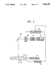
- FIG. 1A is a diagram showing a fundamental construction of means for forming a hole into a printed circuit board in the first embodiment according to the invention
- FIG. 1B is a block diagram for the control regarding the apparatus shown in FIG. 1A;
- FIG. 1C is a schematic diagram showing a state in which a hole is formed by the hole forming method shown in FIG. 1A;
- FIG. 2 is a schematic cross sectional view showing a comparison example of an embodiment according to the invention.
- FIGS. 3 to 5 show the first embodiment
- FIG. 3 is an explanatory diagram of a construction of an apparatus
- FIG. 4 is an explanatory diagram of a working state
- FIG. 5 is an explanatory diagram to check a penetrating state
- FIGS. 6A and 6B show the third embodiment
- FIG. 6A is an explanatory diagram of a construction of an apparatus
- FIG. 6B is an explanatory diagram to check a penetrating state
- FIGS. 7A and 7B are diagrams showing a conventional hole forming method using a drill.
- FIG. 1A is a diagram showing a fundamental construction of means for forming a hole into a printed circuit board in an embodiment according to the invention.
- reference numeral 1 denotes a laser source.
- a laser beam generated from the laser source 1 is reflected by a total reflecting mirror 2 and passes through a condenser lens 4 and is focused to the workpiece 6 (glass-epoxy material for a printed circuit board: TLC-W-551, made by Toshiba Chemicals Co., Ltd.), thereby forming a hole into the workpiece.
- reference numeral 7 denotes a stage (X-Y table) to hole the board.
- the condenser lens 4 is attached to a Z-axis stage 3 equipped with a pulse motor.
- the stage 7 is further controlled by a focusing and laser oscillation control unit 5.
- a signal to start the laser oscillation and a signal to start the descending operation of the pulse motor stage are generated from the control unit 5.
- the condenser lens 4 descends interlockingly with the laser oscillation, so that a focal point of the laser beam obtained by the condenser lens 4 is set to the working position and a hole can be formed.
- FIG. 1B is a block diagram showing the operation of the apparatus shown in FIG. 1A.
- the coordinates of the X-Y table of the stage 7 are moved and the workpiece (board) 6 is set to the focal point position cf the laser beam. Further, a movement amount in the Z-axis direction to set the working surface of the workpiece 6 to the focal point on the Z axis is calculated by a control computer (computer to actuate the stage; not shown) and a command is given to a driver unit of the Z-axis stage.
- a control computer computer to actuate the stage; not shown
- a command is given to a driver unit of the Z-axis stage.
- pulses are output to a pulse motor (not shown) to drive in the Z-axis direction, thereby moving the Z-axis stage to the calculated position in the Z-axis direction.
- the driver unit is stopped.
- a beam output command is generated from the control unit 5 to the laser source 1.
- the laser beams of a predetermined number of pulses is output to execute the hole forming process.
- the stage 7 is returned to the home position or saved position. Thereafter, the workpiece 6 is removed from the stage 7.
- FIG. 1C schematically illustrates a hole forming process in FIGS. 1A and 1B.
- the condenser lens 4 is located at a position 4-1 and a focal point is located on the surface of the board 6.
- the lens 4 is moves from a position 4-2 (focal point is located near the center in the thickness direction of the board 6) to a position 4-3 (focal point is located on the back surface of the board 6) by the control unit 5. Due to this, the center of the beam spot is always located on the working surface, so that a uniform straight through hole 8 is obtained.
- a laser beam such as a CO 2 laser, excimer laser, or the like has been used as an energy source which is used for the hole forming process
- other energy beams such as electron beam, ion beam, or the like can be also used.
- the focal point position has been moved by moving the optical system (mainly, condenser lens) in the optical axis direction.
- a focal distance can be also changed by adjusting a thickness of lens.
- the working by the embodiment has been limited to the hole forming process the invention can be also applied to other workings such as cutting, welding, and the like.
- FIG. 2 shows a process in the case where the lens is fixed and the focal point position is fixed as in the conventional one as a comparison example of the above embodiment. It will be understood that a tapered hole 8' is easily formed by the method in the comparison example.
- the position of the focal point at which the energy density is highest and the beam spot is minimum is moved with the progressing of the hole forming process in the depth direction of the hole forming surface, so that a straight hole shape is obtained and a through hole shape of a high reliability can be obtained.
- FIGS. 3 and 4 show the second embodiments of the invention.
- FIG. 3 is a diagram showing a construction of an apparatus for executing the method of the invention.
- FIG. 4 is a pulse waveform diagram of a laser output in the embodiment.
- FIG. 5 is a diagram showing a working state.
- reference numeral 10 denotes a printed circuit board to be worked; 12 an X-Y table stage which holds the board 10 and can move the board 10 in the directions of the X and Y axes for a predetermined plane; and 14 a driving means such as a motor or the like for driving the X-Y table stage 12.
- Reference numeral 16 denotes a first laser source for generating a first laser beam in a long wavelength range such as a CO 2 gas laser or the like; 18 an optical system to control the light flux of the first laser beam; 20 a reflecting mirror for changing the optical path of the laser beam which passed through the optical system 18 to the working surface of the printed circuit board 10; and 22 a pulse generator to output exciting pulses to drive and excite the first laser source 16.
- a first laser source for generating a first laser beam in a long wavelength range such as a CO 2 gas laser or the like
- 18 an optical system to control the light flux of the first laser beam
- 20 a reflecting mirror for changing the optical path of the laser beam which passed through the optical system 18 to the working surface of the printed circuit board 10
- 22 a pulse generator to output exciting pulses to drive and excite the first laser source 16.
- Reference numeral 15 denotes processing means for processing the output pulses from the first pulse generator 22.
- the processing means 15 receives the pulse signal from the pulse generator 22 and processes it into a signal as shown in FIG. 4.
- Reference numeral 24 denotes a photo sensitive device to detect the light of the bean. As shown in FIG. 5, the photo sensitive device 24 is arranged at a position such as to detect the peripheral light of the light flux which penetrated a copper foil portion 1C of the back surface of the printed circuit board by a beam R.
- Reference numeral 26 in FIG. 3 denotes an amplifier for amplifying a signal from the photo sensitive device 24 and outputting a signal to inhibit the pulse generation to the pulse generator 22.
- the processing means 15 When driving pulses of a predetermined period are output from the pulse generator by a driving signal S 1 , the processing means 15 outputs exciting pulses of the laser source as shown in FIG. 4 by the reception of the driving pulses.
- a time base is set from the right to the left on an axis of abscissa and an output level of the exciting pulse is set to an axis of ordinate.
- an exciting pulse P 1 of a large output is generated.
- the large exciting pulse P 1 is a pulse to form a hole into the copper foil portion of the surface of the printed circuit board.
- the number of exciting pulses P 1 is properly set to one or a plural number.
- a plurality of low output pulses P 2 to P 6 are output.
- the low output waveform pulses P 2 to P 6 are exciting pulses to work the portion of the resin material under the copper foil portion of the front surface after they penetrated the copper foil portion of the surface of the printed circuit board.
- the exciting pulses P 2 to P 6 to work the resin portion are set so as to gradually increase the pulse outputs and to gradually reduce the pulse widths.
- large output exciting pulses P 7 , P 8 , . . . which are similar to the initial oscillating pulses P 1 are output.
- the large output exciting pulses P 7 , P 8 , . . . are used to work the copper foil portion of the back surface of the printed circuit board.
- the pulses P 1 to P 8 shown in FIG. 4 are generated from the laser source 16 by the pulse processing mean: 15 and a through hole is formed in the printed circuit board. After the hole was penetrated, the laser beam passes through the through hole and is irradiated and enters the photo sensitive device 24 arranged at the position such as to detect the peripheral light flux of an optical axis O 1 of the beam.
- the photo sensitive device 24 receives the incident light and outputs an electric signal.
- the electric signal is input to the amplifier 26.
- the amplified signal from the amplifier 26 is input to the pulse generator 22 and the operation to inhibit the pulse generation is performed, so that the laser output is stopped.
- the photo sensitive device has been arranged on the through hole side (back surface side) of the printed circuit board.
- the photo sensitive device can be also arranged above the printed circuit board and the weak peripheral light of the beam light flux can be also detected.
- FIG. 6A is a diagram showing a fundamental construction of means for forming holes into a printed circuit board of the embodiment according to the invention.
- reference numeral 31 denotes a laser source.
- a laser beam generated from the laser source 31 is reflected by a total reflecting mirror 32 and passes through a condenser lens 34 and is focused onto a workpiece 36 (glass-epoxy material for a printed circuit board: TLC-W-551, made by Toshiba Chemicals Co., Ltd.), thereby forming a hole into the workpiece.
- reference numeral 37 denotes a stage to hold the board.
- the condenser lens 34 is attached to a Z-axis stage 33 equipped with a pulse motor.
- the stage 37 is further controlled by a focusing and laser oscillation control unit 35.
- a signal to start the laser oscillation and a signal to start the descending of the pulse motor stage are output from the control unit 35. Since the condenser lens 34 descends interlockingly with the laser oscillation, a focal point of the laser beam obtained by the condenser lens 34 is set to the working position, so that a hole can be formed.
- FIG. 6B schematically shows a hole forming state in the above apparatus.
- the condenser lens 34 is located at the position 4-1 and the focal point is located on the surface of the board 36.
- the lens 34 is moved from the position 4-2 (the focal point is located near the center in the thickness direction of the board 36) to the position 4-3 (the focal point is located on the back surface of the board 36) by the control unit 35. Due to this, the center of the beam spot is always located on the working surface, so that a uniform straight through hole 38 can be obtained.
- Position detecting sensors S 1 , S 2 and S 3 are arranged near the Z-axis stage 33.
- the sensor S 1 detects the start position (4-1) of a holding member 34A of the lens 34.
- the sensor S 2 detects the penetrating position shown in FIG. 6B.
- the sensor S 2 outputs a detection signal to an amplifier 38 1 .
- the amplifier 38 1 receives the signal from the sensor S 2
- the amplifier 38 1 outputs a signal to the laser source 31 and control unit 35.
- the laser source 31 receives the signal from the amplifier 38 1 , the output of the laser beam is weakened and the operating mode is switched so as to generate a laser to check the penetration.
- the control unit 35 further descends the lens 34 until a position 4-4 shown in FIG. 6B.
- the sensor S 3 outputs a confirmation signal of the lens descending position, the laser beam of a weakened output is generated in response to the signal of the sensor S 3 .
- a photo sensitive device 40 to detect the beam light of the weakened output is arranged below the printed circuit board 36 as shown in FIG. 6B.
- the photo sensitive device 40 which detected the weak light confirms the penetrating state of the printed circuit board 36 and outputs a detection signal.
- the signal of the device 40 is amplified by an amplifier 42. After that, the amplified signal is sent to the control unit 35, thereby stopping the laser oscillation.
- the penetrating state is checked by using the photo sensitive device and the laser generation is stopped after the penetration was confirmed, so that a through hole having a uniform diameter can be obtained.
- the penetration can be accurately confirmed.
Abstract
Description
Claims (4)
Applications Claiming Priority (4)
| Application Number | Priority Date | Filing Date | Title |
|---|---|---|---|
| JP1188971A JPH0357585A (en) | 1989-07-24 | 1989-07-24 | Method and device for piercing printed circuit board |
| JP1-188971 | 1989-07-24 | ||
| JP2-154685 | 1990-06-12 | ||
| JP2154685A JPH0445593A (en) | 1990-06-12 | 1990-06-12 | Confirming method for boring of printed wiring board |
Publications (1)
| Publication Number | Publication Date |
|---|---|
| US5063280A true US5063280A (en) | 1991-11-05 |
Family
ID=26482901
Family Applications (1)
| Application Number | Title | Priority Date | Filing Date |
|---|---|---|---|
| US07/553,666 Expired - Lifetime US5063280A (en) | 1989-07-24 | 1990-07-18 | Method and apparatus for forming holes into printed circuit board |
Country Status (1)
| Country | Link |
|---|---|
| US (1) | US5063280A (en) |
Cited By (67)
| Publication number | Priority date | Publication date | Assignee | Title |
|---|---|---|---|---|
| US5194711A (en) * | 1988-08-15 | 1993-03-16 | Anstalt Gersan | Cutting using high energy radiation |
| US5237148A (en) * | 1990-10-04 | 1993-08-17 | Brother Kogyo Kabushiki | Device for manufacturing a nozzle and its manufacturing method |
| US5293025A (en) * | 1991-08-01 | 1994-03-08 | E. I. Du Pont De Nemours And Company | Method for forming vias in multilayer circuits |
| US5302798A (en) * | 1991-04-01 | 1994-04-12 | Canon Kabushiki Kaisha | Method of forming a hole with a laser and an apparatus for forming a hole with a laser |
| US5332881A (en) * | 1991-09-03 | 1994-07-26 | Weidmuller Interface GmbH & Company | Tool head with an automatically adjustable optical focusing system |
| US5334815A (en) * | 1992-01-15 | 1994-08-02 | Wear Guard Corp. | Apparatus and method for producing a printing screen |
| US5349155A (en) * | 1992-01-17 | 1994-09-20 | Fujitsu Limited | Insulating material for wiring substrate and method of producing multi-layered wiring substrate |
| US5376770A (en) * | 1992-01-13 | 1994-12-27 | Maho Aktiengesellschaft | Process and device for machining workpieces by means of a laser beam |
| US5585017A (en) * | 1993-09-13 | 1996-12-17 | James; William A. | Defocused laser drilling process for forming a support member of a fabric forming device |
| US5593606A (en) * | 1994-07-18 | 1997-01-14 | Electro Scientific Industries, Inc. | Ultraviolet laser system and method for forming vias in multi-layered targets |
| US5614114A (en) * | 1994-07-18 | 1997-03-25 | Electro Scientific Industries, Inc. | Laser system and method for plating vias |
| US5626777A (en) * | 1993-03-02 | 1997-05-06 | Hoechst Ceramtec Ag | Process for producing dividable plates of brittle material with high accuracy and apparatus for receiving and precision-grinding the end faces of a plate |
| EP0807484A1 (en) * | 1996-05-16 | 1997-11-19 | British Aerospace Public Limited Company | Method and apparatus for drilling a hole in solid material by laser beam irradiation |
| US5790383A (en) * | 1996-02-20 | 1998-08-04 | Canon Kabushiki Kaisha | Printed circuit board |
| US5841099A (en) * | 1994-07-18 | 1998-11-24 | Electro Scientific Industries, Inc. | Method employing UV laser pulses of varied energy density to form depthwise self-limiting blind vias in multilayered targets |
| EP0884128A1 (en) * | 1996-11-20 | 1998-12-16 | Ibiden Co., Ltd. | Laser machining apparatus, and apparatus and method for manufacturing a multilayered printed wiring board |
| US5916462A (en) * | 1993-09-13 | 1999-06-29 | James; William A. | Laser drilling processes for forming an apertured film |
| US5976124A (en) * | 1998-01-05 | 1999-11-02 | Spectranetics Corporation | Phototherapy device and method |
| EP0964610A2 (en) * | 1998-06-02 | 1999-12-15 | Mitsubishi Gas Chemical Company, Inc. | Printed wiring board and process for forming it |
| GB2338443A (en) * | 1998-06-18 | 1999-12-22 | Gen Electric | Laser drilling breakthrough detector |
| EP0980737A1 (en) * | 1997-12-12 | 2000-02-23 | Matsushita Electric Industrial Co., Ltd. | Laser machining method, laser machining device and control method of laser machining |
| WO2000041447A1 (en) * | 1999-01-05 | 2000-07-13 | Ppc Electronic Ag | Method for producing a multilayer printed circuit board |
| US6158843A (en) * | 1997-03-28 | 2000-12-12 | Lexmark International, Inc. | Ink jet printer nozzle plates with ink filtering projections |
| US6175096B1 (en) * | 1996-09-30 | 2001-01-16 | Force Instituttet | Method of processing a material by means of a laser beam |
| US6183064B1 (en) | 1995-08-28 | 2001-02-06 | Lexmark International, Inc. | Method for singulating and attaching nozzle plates to printheads |
| US6215076B1 (en) | 1996-03-28 | 2001-04-10 | Canon Kabushiki Kaisha | Printed circuit board with noise suppression |
| US6228311B1 (en) * | 1996-01-18 | 2001-05-08 | Xaar Technology Limited | Method of and apparatus for forming nozzles |
| EP1121008A1 (en) * | 1998-09-03 | 2001-08-01 | Ibiden Co., Ltd. | Multilayer printed wiring board and method for manufacturing the same |
| US6283584B1 (en) | 2000-04-18 | 2001-09-04 | Lexmark International, Inc. | Ink jet flow distribution system for ink jet printer |
| US6373070B1 (en) | 1999-10-12 | 2002-04-16 | Fei Company | Method apparatus for a coaxial optical microscope with focused ion beam |
| US6407363B2 (en) | 2000-03-30 | 2002-06-18 | Electro Scientific Industries, Inc. | Laser system and method for single press micromachining of multilayer workpieces |
| US6462306B1 (en) | 1999-04-27 | 2002-10-08 | Gsi Lumonics, Inc. | System and method for material processing using multiple laser beams |
| US6479788B1 (en) * | 1997-11-10 | 2002-11-12 | Hitachi Via Mechanics, Ltd. | Method and apparatus of making a hole in a printed circuit board |
| US20030006220A1 (en) * | 2001-07-02 | 2003-01-09 | Michael Cummings | Method of ablating an opening in a hard, non-metallic substrate |
| WO2003015482A2 (en) * | 2001-08-09 | 2003-02-20 | Orbotech Ltd. | A system and method for unveiling targets embedded in a multi-layered electrical circuit |
| EP1295647A1 (en) * | 2001-09-24 | 2003-03-26 | The Technology Partnership Public Limited Company | Nozzles in perforate membranes and their manufacture |
| US20030102436A1 (en) * | 2000-03-20 | 2003-06-05 | Gerard Benas-Sayag | Column simultaneously focusing a particle beam and an optical beam |
| US6623103B2 (en) | 2001-04-10 | 2003-09-23 | Lexmark International, Inc. | Laser ablation method for uniform nozzle structure |
| WO2004011187A1 (en) * | 2002-07-25 | 2004-02-05 | Matsushita Electric Industrial Co., Ltd. | System and method of laser drilling using a continuously optimized depth of focus |
| US6720567B2 (en) | 2001-01-30 | 2004-04-13 | Gsi Lumonics Corporation | Apparatus and method for focal point control for laser machining |
| US20040070754A1 (en) * | 1999-06-10 | 2004-04-15 | Aradigm Corporation | Method and device for non-destructive analysis of perforations in a material |
| US6777641B2 (en) | 2002-04-16 | 2004-08-17 | W.A. Whitney Co. | Method and apparatus for laser piercing and cutting metal sheet and plate |
| US6777103B2 (en) | 2000-10-17 | 2004-08-17 | James Hardie Research Pty Limited | Fiber cement composite material using biocide treated durable cellulose fibers |
| US20040173942A1 (en) * | 2001-05-11 | 2004-09-09 | Nobutaka Kobayashi | Method and device for laser beam machining of laminated material |
| US20040222197A1 (en) * | 1996-11-20 | 2004-11-11 | Ibiden Co., Ltd. | Laser machining apparatus, and apparatus and method for manufacturing a multilayered printed wiring board |
| EP1525069A1 (en) * | 2002-07-25 | 2005-04-27 | Matsushita Electric Industrial Co., Ltd. | System and method of laser drilling using a continuously optimized depth of focus |
| US20050230370A1 (en) * | 2004-04-15 | 2005-10-20 | Denso Corporation | Laser beam machining equipment and method for machining by using laser beam |
| US20060128120A1 (en) * | 2004-12-14 | 2006-06-15 | Chih-Ming Hsu | Short-wavelength laser dicing apparatus for a diamond wafer and dicing method thereof |
| US20060249496A1 (en) * | 2005-05-09 | 2006-11-09 | Disco Corporation | Processing method and apparatus using laser beam |
| US20070019187A1 (en) * | 1999-06-10 | 2007-01-25 | Aradigm Corporation | Method and device for non-destructive analysis of perforations in a material |
| WO2009023279A1 (en) * | 2007-08-15 | 2009-02-19 | Caterpillar Inc. | Variable focus laser machining system |
| AU2003258227B2 (en) * | 2003-08-14 | 2009-04-23 | Aradigm Corporation | Method and device for non-destructive analysis of perforations in a material |
| US20090294416A1 (en) * | 2008-05-28 | 2009-12-03 | Caterpillar Inc. | Laser manufacturing system having real-time feedback |
| US20090325322A1 (en) * | 2008-06-25 | 2009-12-31 | Joseph Martin Patterson | Non-Destructive Laser Optical Integrated Circuit Package Marking |
| US20110017716A1 (en) * | 2008-02-19 | 2011-01-27 | M-Solv Limited | Laser processing a multi-device panel |
| US20110100967A1 (en) * | 2009-11-03 | 2011-05-05 | Applied Spectra, Inc. | Method for real-time optical diagnostics in laser ablation and laser processing of layered and structured materials |
| US20110147351A1 (en) * | 2008-06-04 | 2011-06-23 | Mitsubishi Electric Corporation | Laser processing apparatus and laser processing method |
| US20120211477A1 (en) * | 2011-02-20 | 2012-08-23 | Electro Scientific Industries, Inc. | Method and apparatus for improved laser scribing of opto-electric devices |
| CN102814591A (en) * | 2012-05-23 | 2012-12-12 | 苏州德龙激光有限公司 | Laser processing method and laser processing equipment |
| US20140053399A1 (en) * | 2012-08-27 | 2014-02-27 | Micronic Mydata AB | Maskless writing of a workpiece using a plurality of exposures having different focal planes using multiple dmds |
| US20160001397A1 (en) * | 2014-07-03 | 2016-01-07 | Microinspection, Inc. | Laser processing apparatus |
| US20170326688A1 (en) * | 2015-01-29 | 2017-11-16 | Imra America, Inc. | Laser-based modification of transparent materials |
| US20180086078A1 (en) * | 2016-09-26 | 2018-03-29 | Sii Printek Inc. | Method for manufacturing ejection hole plate |
| US20190106994A1 (en) * | 2017-10-05 | 2019-04-11 | United Technologies Corporation | Multi-step clearance of coating |
| DE102019108131A1 (en) * | 2019-03-28 | 2020-10-01 | Pulsar Photonics Gmbh | Device and method for forming VIA laser bores |
| US20220314369A1 (en) * | 2021-03-31 | 2022-10-06 | Yangtze Memory Technologies Co., Ltd. | Laser system for dicing semiconductor structure and operation method thereof |
| US11839914B1 (en) | 2019-01-31 | 2023-12-12 | Freeform Future Corp. | Process monitoring and feedback for metal additive manufacturing using powder-bed fusion |
Citations (5)
| Publication number | Priority date | Publication date | Assignee | Title |
|---|---|---|---|---|
| US4088864A (en) * | 1974-11-18 | 1978-05-09 | Alza Corporation | Process for forming outlet passageways in pills using a laser |
| US4263495A (en) * | 1975-01-28 | 1981-04-21 | Hitachi, Ltd. | Method of splicing optical fibers by CO2 -laser |
| JPS5850190A (en) * | 1981-09-22 | 1983-03-24 | Agency Of Ind Science & Technol | Inspecting method for cutting condition |
| US4873414A (en) * | 1988-06-13 | 1989-10-10 | Rolls Royce Inc. | Laser drilling of components |
| US4933045A (en) * | 1989-06-02 | 1990-06-12 | International Business Machines Corporation | Thin film multilayer laminate interconnection board assembly method |
-
1990
- 1990-07-18 US US07/553,666 patent/US5063280A/en not_active Expired - Lifetime
Patent Citations (5)
| Publication number | Priority date | Publication date | Assignee | Title |
|---|---|---|---|---|
| US4088864A (en) * | 1974-11-18 | 1978-05-09 | Alza Corporation | Process for forming outlet passageways in pills using a laser |
| US4263495A (en) * | 1975-01-28 | 1981-04-21 | Hitachi, Ltd. | Method of splicing optical fibers by CO2 -laser |
| JPS5850190A (en) * | 1981-09-22 | 1983-03-24 | Agency Of Ind Science & Technol | Inspecting method for cutting condition |
| US4873414A (en) * | 1988-06-13 | 1989-10-10 | Rolls Royce Inc. | Laser drilling of components |
| US4933045A (en) * | 1989-06-02 | 1990-06-12 | International Business Machines Corporation | Thin film multilayer laminate interconnection board assembly method |
Cited By (121)
| Publication number | Priority date | Publication date | Assignee | Title |
|---|---|---|---|---|
| US5194711A (en) * | 1988-08-15 | 1993-03-16 | Anstalt Gersan | Cutting using high energy radiation |
| US5237148A (en) * | 1990-10-04 | 1993-08-17 | Brother Kogyo Kabushiki | Device for manufacturing a nozzle and its manufacturing method |
| US5302798A (en) * | 1991-04-01 | 1994-04-12 | Canon Kabushiki Kaisha | Method of forming a hole with a laser and an apparatus for forming a hole with a laser |
| US5293025A (en) * | 1991-08-01 | 1994-03-08 | E. I. Du Pont De Nemours And Company | Method for forming vias in multilayer circuits |
| US5332881A (en) * | 1991-09-03 | 1994-07-26 | Weidmuller Interface GmbH & Company | Tool head with an automatically adjustable optical focusing system |
| US5376770A (en) * | 1992-01-13 | 1994-12-27 | Maho Aktiengesellschaft | Process and device for machining workpieces by means of a laser beam |
| US5334815A (en) * | 1992-01-15 | 1994-08-02 | Wear Guard Corp. | Apparatus and method for producing a printing screen |
| US5349155A (en) * | 1992-01-17 | 1994-09-20 | Fujitsu Limited | Insulating material for wiring substrate and method of producing multi-layered wiring substrate |
| US5626777A (en) * | 1993-03-02 | 1997-05-06 | Hoechst Ceramtec Ag | Process for producing dividable plates of brittle material with high accuracy and apparatus for receiving and precision-grinding the end faces of a plate |
| US5585017A (en) * | 1993-09-13 | 1996-12-17 | James; William A. | Defocused laser drilling process for forming a support member of a fabric forming device |
| US5916462A (en) * | 1993-09-13 | 1999-06-29 | James; William A. | Laser drilling processes for forming an apertured film |
| US5614114A (en) * | 1994-07-18 | 1997-03-25 | Electro Scientific Industries, Inc. | Laser system and method for plating vias |
| EP0771243A1 (en) | 1994-07-18 | 1997-05-07 | Electro Scientific Industries, Inc. | Ultraviolet laser system and method for forming vias in multi-layered targets |
| US5841099A (en) * | 1994-07-18 | 1998-11-24 | Electro Scientific Industries, Inc. | Method employing UV laser pulses of varied energy density to form depthwise self-limiting blind vias in multilayered targets |
| US5593606A (en) * | 1994-07-18 | 1997-01-14 | Electro Scientific Industries, Inc. | Ultraviolet laser system and method for forming vias in multi-layered targets |
| US6183064B1 (en) | 1995-08-28 | 2001-02-06 | Lexmark International, Inc. | Method for singulating and attaching nozzle plates to printheads |
| US6323456B1 (en) | 1995-08-28 | 2001-11-27 | Lexmark International, Inc. | Method of forming an ink jet printhead structure |
| US7473387B2 (en) | 1996-01-18 | 2009-01-06 | Xaar Technology Limited | Method of and apparatus for forming nozzles |
| US20050206041A1 (en) * | 1996-01-18 | 2005-09-22 | Xaar Technology Limited | Method of forming nozzles |
| US6228311B1 (en) * | 1996-01-18 | 2001-05-08 | Xaar Technology Limited | Method of and apparatus for forming nozzles |
| US5790383A (en) * | 1996-02-20 | 1998-08-04 | Canon Kabushiki Kaisha | Printed circuit board |
| US6215076B1 (en) | 1996-03-28 | 2001-04-10 | Canon Kabushiki Kaisha | Printed circuit board with noise suppression |
| EP0807484A1 (en) * | 1996-05-16 | 1997-11-19 | British Aerospace Public Limited Company | Method and apparatus for drilling a hole in solid material by laser beam irradiation |
| US6175096B1 (en) * | 1996-09-30 | 2001-01-16 | Force Instituttet | Method of processing a material by means of a laser beam |
| US7462802B2 (en) | 1996-11-20 | 2008-12-09 | Ibiden Co., Ltd. | Laser machining apparatus, and apparatus and method for manufacturing a multilayered printed wiring board |
| US20040222197A1 (en) * | 1996-11-20 | 2004-11-11 | Ibiden Co., Ltd. | Laser machining apparatus, and apparatus and method for manufacturing a multilayered printed wiring board |
| US7732732B2 (en) | 1996-11-20 | 2010-06-08 | Ibiden Co., Ltd. | Laser machining apparatus, and apparatus and method for manufacturing a multilayered printed wiring board |
| US20060138098A1 (en) * | 1996-11-20 | 2006-06-29 | Ibiden Co., Ltd. | Laser machining apparatus, and apparatus and method for manufacturing a multilayered printed wiring board |
| US7456372B2 (en) | 1996-11-20 | 2008-11-25 | Ibiden Co., Ltd. | Laser machining apparatus, and apparatus and method for manufacturing a multilayered printed wiring board |
| US7462801B1 (en) | 1996-11-20 | 2008-12-09 | Ibiden Co., Ltd. | Laser machining apparatus, and apparatus and method for manufacturing a multilayered printed wiring board |
| US7667160B2 (en) | 1996-11-20 | 2010-02-23 | Ibiden Co., Ltd | Laser machining apparatus, and apparatus and method for manufacturing a multilayered printed wiring board |
| EP0884128A4 (en) * | 1996-11-20 | 2000-12-20 | Ibiden Co Ltd | Laser machining apparatus, and apparatus and method for manufacturing a multilayered printed wiring board |
| US20050263498A1 (en) * | 1996-11-20 | 2005-12-01 | Ibiden Co., Ltd. | Ceramic heater |
| US20060138097A1 (en) * | 1996-11-20 | 2006-06-29 | Ibiden Co., Ltd. | Laser machining apparatus, and apparatus and method for manufacturing a multilayered printed wiring board |
| EP0884128A1 (en) * | 1996-11-20 | 1998-12-16 | Ibiden Co., Ltd. | Laser machining apparatus, and apparatus and method for manufacturing a multilayered printed wiring board |
| CN1103688C (en) * | 1997-03-28 | 2003-03-26 | 莱克斯马克国际公司 | Ink jet printer nozzle plates |
| US6158843A (en) * | 1997-03-28 | 2000-12-12 | Lexmark International, Inc. | Ink jet printer nozzle plates with ink filtering projections |
| US6479788B1 (en) * | 1997-11-10 | 2002-11-12 | Hitachi Via Mechanics, Ltd. | Method and apparatus of making a hole in a printed circuit board |
| US6586703B2 (en) | 1997-12-12 | 2003-07-01 | Matsushita Electric Industrial Co., Ltd. | Laser machining method, laser machining apparatus, and its control method |
| US6441337B1 (en) | 1997-12-12 | 2002-08-27 | Matsushita Electric Industrial Co., Ltd. | Laser machining method, laser machining device and control method of laser machining |
| EP0980737A1 (en) * | 1997-12-12 | 2000-02-23 | Matsushita Electric Industrial Co., Ltd. | Laser machining method, laser machining device and control method of laser machining |
| EP0980737A4 (en) * | 1997-12-12 | 2002-07-31 | Matsushita Electric Ind Co Ltd | Laser machining method, laser machining device and control method of laser machining |
| US5976124A (en) * | 1998-01-05 | 1999-11-02 | Spectranetics Corporation | Phototherapy device and method |
| EP0964610A2 (en) * | 1998-06-02 | 1999-12-15 | Mitsubishi Gas Chemical Company, Inc. | Printed wiring board and process for forming it |
| EP0964610A3 (en) * | 1998-06-02 | 2001-03-21 | Mitsubishi Gas Chemical Company, Inc. | Printed wiring board and process for forming it |
| US6280641B1 (en) | 1998-06-02 | 2001-08-28 | Mitsubishi Gas Chemical Company, Inc. | Printed wiring board having highly reliably via hole and process for forming via hole |
| GB2338443B (en) * | 1998-06-18 | 2003-02-12 | Gen Electric | Laser drilling breakthrough detector |
| GB2338443A (en) * | 1998-06-18 | 1999-12-22 | Gen Electric | Laser drilling breakthrough detector |
| US6140604A (en) * | 1998-06-18 | 2000-10-31 | General Electric Company | Laser drilling breakthrough detector |
| EP1121008A4 (en) * | 1998-09-03 | 2005-02-02 | Ibiden Co Ltd | Multilayer printed wiring board and method for manufacturing the same |
| EP1121008A1 (en) * | 1998-09-03 | 2001-08-01 | Ibiden Co., Ltd. | Multilayer printed wiring board and method for manufacturing the same |
| US20080173473A1 (en) * | 1998-09-03 | 2008-07-24 | Ibiden Co., Ltd | Multilayered printed circuit board and manufacturing method thereof |
| US20040025333A1 (en) * | 1998-09-03 | 2004-02-12 | Ibiden Co., Ltd. | Multilayered printed circuit board and manufacturing method therefor |
| US7832098B2 (en) | 1998-09-03 | 2010-11-16 | Ibiden Co., Ltd. | Method of manufacturing a multilayered printed circuit board |
| US8148643B2 (en) | 1998-09-03 | 2012-04-03 | Ibiden Co., Ltd. | Multilayered printed circuit board and manufacturing method thereof |
| US7415761B2 (en) | 1998-09-03 | 2008-08-26 | Ibiden Co., Ltd. | Method of manufacturing multilayered circuit board |
| WO2000041447A1 (en) * | 1999-01-05 | 2000-07-13 | Ppc Electronic Ag | Method for producing a multilayer printed circuit board |
| US6462306B1 (en) | 1999-04-27 | 2002-10-08 | Gsi Lumonics, Inc. | System and method for material processing using multiple laser beams |
| US20040070754A1 (en) * | 1999-06-10 | 2004-04-15 | Aradigm Corporation | Method and device for non-destructive analysis of perforations in a material |
| US7301621B2 (en) | 1999-06-10 | 2007-11-27 | Aradigm Corporation | Method and device for non-destructive analysis of perforations in a material |
| US7148960B2 (en) * | 1999-06-10 | 2006-12-12 | Aradigm Corporation | Method and device for non-destructive analysis of perforations in a material |
| US20070019187A1 (en) * | 1999-06-10 | 2007-01-25 | Aradigm Corporation | Method and device for non-destructive analysis of perforations in a material |
| US20080085940A1 (en) * | 1999-06-10 | 2008-04-10 | Aradigm Corporation | Method and device for non-destructive analysis of perforations in a material |
| US6373070B1 (en) | 1999-10-12 | 2002-04-16 | Fei Company | Method apparatus for a coaxial optical microscope with focused ion beam |
| US20030102436A1 (en) * | 2000-03-20 | 2003-06-05 | Gerard Benas-Sayag | Column simultaneously focusing a particle beam and an optical beam |
| US7297948B2 (en) | 2000-03-20 | 2007-11-20 | Credence Systems Corporation | Column simultaneously focusing a particle beam and an optical beam |
| US20060097198A1 (en) * | 2000-03-20 | 2006-05-11 | Gerard Benas-Sayag | Column simultaneously focusing a particle beam and an optical beam |
| US6407363B2 (en) | 2000-03-30 | 2002-06-18 | Electro Scientific Industries, Inc. | Laser system and method for single press micromachining of multilayer workpieces |
| US6283584B1 (en) | 2000-04-18 | 2001-09-04 | Lexmark International, Inc. | Ink jet flow distribution system for ink jet printer |
| US6777103B2 (en) | 2000-10-17 | 2004-08-17 | James Hardie Research Pty Limited | Fiber cement composite material using biocide treated durable cellulose fibers |
| US6720567B2 (en) | 2001-01-30 | 2004-04-13 | Gsi Lumonics Corporation | Apparatus and method for focal point control for laser machining |
| US6623103B2 (en) | 2001-04-10 | 2003-09-23 | Lexmark International, Inc. | Laser ablation method for uniform nozzle structure |
| US20040173942A1 (en) * | 2001-05-11 | 2004-09-09 | Nobutaka Kobayashi | Method and device for laser beam machining of laminated material |
| US6864460B2 (en) * | 2001-07-02 | 2005-03-08 | Virtek Laser Systems, Inc. | Method of ablating an opening in a hard, non-metallic substrate |
| US20030006220A1 (en) * | 2001-07-02 | 2003-01-09 | Michael Cummings | Method of ablating an opening in a hard, non-metallic substrate |
| WO2003004210A1 (en) * | 2001-07-02 | 2003-01-16 | Virtek Laser Systems, Inc. | Method of ablating an opening in a hard, non-metallic substrate |
| KR100852155B1 (en) | 2001-07-02 | 2008-08-13 | 버텍 비젼 인터내셔널 인코포레이티드 | Method of ablating an opening in a hard, non-metallic substrate |
| CN1308113C (en) * | 2001-07-02 | 2007-04-04 | 维蒂克激光系统公司 | Method of ablating an opening in a hard, non-metallic substrate |
| EP1409192A4 (en) * | 2001-07-02 | 2008-08-06 | Virtek Laser Systems Inc | Method of ablating an opening in a hard, non-metallic substrate |
| EP1409192A1 (en) * | 2001-07-02 | 2004-04-21 | Virtek Laser Systems, Inc. | Method of ablating an opening in a hard, non-metallic substrate |
| US6911620B2 (en) | 2001-08-09 | 2005-06-28 | Orbotech, Ltd. | System and method for unveiling targets embedded in a multi-layered electrical circuit |
| US20030052099A1 (en) * | 2001-08-09 | 2003-03-20 | Orbotech Ltd. | System and method for unveiling targets embedded in a multi-layered electrical circuit |
| WO2003015482A2 (en) * | 2001-08-09 | 2003-02-20 | Orbotech Ltd. | A system and method for unveiling targets embedded in a multi-layered electrical circuit |
| KR100969452B1 (en) | 2001-08-09 | 2010-07-14 | 오르보테크 엘티디. | A system and method for unveiling targets embedded in a multi-layered electrical circuit |
| WO2003015482A3 (en) * | 2001-08-09 | 2003-10-09 | Orbotech Ltd | A system and method for unveiling targets embedded in a multi-layered electrical circuit |
| EP1295647A1 (en) * | 2001-09-24 | 2003-03-26 | The Technology Partnership Public Limited Company | Nozzles in perforate membranes and their manufacture |
| US6777641B2 (en) | 2002-04-16 | 2004-08-17 | W.A. Whitney Co. | Method and apparatus for laser piercing and cutting metal sheet and plate |
| EP1525069A1 (en) * | 2002-07-25 | 2005-04-27 | Matsushita Electric Industrial Co., Ltd. | System and method of laser drilling using a continuously optimized depth of focus |
| US6787734B2 (en) * | 2002-07-25 | 2004-09-07 | Matsushita Electric Industrial Co., Ltd. | System and method of laser drilling using a continuously optimized depth of focus |
| WO2004011187A1 (en) * | 2002-07-25 | 2004-02-05 | Matsushita Electric Industrial Co., Ltd. | System and method of laser drilling using a continuously optimized depth of focus |
| EP1525069A4 (en) * | 2002-07-25 | 2006-05-24 | Matsushita Electric Ind Co Ltd | System and method of laser drilling using a continuously optimized depth of focus |
| CN1313239C (en) * | 2002-07-25 | 2007-05-02 | 松下电器产业株式会社 | System and method of laser drilling using a continuously optimized depth of focus |
| AU2003258227B2 (en) * | 2003-08-14 | 2009-04-23 | Aradigm Corporation | Method and device for non-destructive analysis of perforations in a material |
| US20050230370A1 (en) * | 2004-04-15 | 2005-10-20 | Denso Corporation | Laser beam machining equipment and method for machining by using laser beam |
| US20060128120A1 (en) * | 2004-12-14 | 2006-06-15 | Chih-Ming Hsu | Short-wavelength laser dicing apparatus for a diamond wafer and dicing method thereof |
| US20060249496A1 (en) * | 2005-05-09 | 2006-11-09 | Disco Corporation | Processing method and apparatus using laser beam |
| WO2009023279A1 (en) * | 2007-08-15 | 2009-02-19 | Caterpillar Inc. | Variable focus laser machining system |
| US20090321395A1 (en) * | 2007-08-15 | 2009-12-31 | Caterpillar Inc. | Variable focus laser machining system |
| US8212177B2 (en) * | 2007-08-15 | 2012-07-03 | Caterpillar Inc. | Variable focus laser machining system |
| US20110017716A1 (en) * | 2008-02-19 | 2011-01-27 | M-Solv Limited | Laser processing a multi-device panel |
| US8710403B2 (en) * | 2008-02-19 | 2014-04-29 | M-Solv Ltd. | Laser processing a multi-device panel |
| US20090294416A1 (en) * | 2008-05-28 | 2009-12-03 | Caterpillar Inc. | Laser manufacturing system having real-time feedback |
| US20110147351A1 (en) * | 2008-06-04 | 2011-06-23 | Mitsubishi Electric Corporation | Laser processing apparatus and laser processing method |
| US20090325322A1 (en) * | 2008-06-25 | 2009-12-31 | Joseph Martin Patterson | Non-Destructive Laser Optical Integrated Circuit Package Marking |
| US7931849B2 (en) * | 2008-06-25 | 2011-04-26 | Applied Micro Circuits Corporation | Non-destructive laser optical integrated circuit package marking |
| US20110100967A1 (en) * | 2009-11-03 | 2011-05-05 | Applied Spectra, Inc. | Method for real-time optical diagnostics in laser ablation and laser processing of layered and structured materials |
| US9061369B2 (en) * | 2009-11-03 | 2015-06-23 | Applied Spectra, Inc. | Method for real-time optical diagnostics in laser ablation and laser processing of layered and structured materials |
| US20120211477A1 (en) * | 2011-02-20 | 2012-08-23 | Electro Scientific Industries, Inc. | Method and apparatus for improved laser scribing of opto-electric devices |
| US8735772B2 (en) * | 2011-02-20 | 2014-05-27 | Electro Scientific Industries, Inc. | Method and apparatus for improved laser scribing of opto-electric devices |
| CN102814591B (en) * | 2012-05-23 | 2016-06-01 | 苏州德龙激光股份有限公司 | Laser processing and laser process equipment |
| CN102814591A (en) * | 2012-05-23 | 2012-12-12 | 苏州德龙激光有限公司 | Laser processing method and laser processing equipment |
| US10149390B2 (en) * | 2012-08-27 | 2018-12-04 | Mycronic AB | Maskless writing of a workpiece using a plurality of exposures having different focal planes using multiple DMDs |
| US20140053399A1 (en) * | 2012-08-27 | 2014-02-27 | Micronic Mydata AB | Maskless writing of a workpiece using a plurality of exposures having different focal planes using multiple dmds |
| US11284517B2 (en) * | 2012-08-27 | 2022-03-22 | Micronic Mydata AB | System for direct writing on an uneven surface of a workpiece that is covered with a radiation sensitive layer using exposures having different focal planes |
| US20160001397A1 (en) * | 2014-07-03 | 2016-01-07 | Microinspection, Inc. | Laser processing apparatus |
| US20170326688A1 (en) * | 2015-01-29 | 2017-11-16 | Imra America, Inc. | Laser-based modification of transparent materials |
| US20180086078A1 (en) * | 2016-09-26 | 2018-03-29 | Sii Printek Inc. | Method for manufacturing ejection hole plate |
| US20190106994A1 (en) * | 2017-10-05 | 2019-04-11 | United Technologies Corporation | Multi-step clearance of coating |
| US11839914B1 (en) | 2019-01-31 | 2023-12-12 | Freeform Future Corp. | Process monitoring and feedback for metal additive manufacturing using powder-bed fusion |
| DE102019108131A1 (en) * | 2019-03-28 | 2020-10-01 | Pulsar Photonics Gmbh | Device and method for forming VIA laser bores |
| US20220314369A1 (en) * | 2021-03-31 | 2022-10-06 | Yangtze Memory Technologies Co., Ltd. | Laser system for dicing semiconductor structure and operation method thereof |
Similar Documents
| Publication | Publication Date | Title |
|---|---|---|
| US5063280A (en) | Method and apparatus for forming holes into printed circuit board | |
| US5073687A (en) | Method and apparatus for working print board by laser | |
| US5126532A (en) | Apparatus and method of boring using laser | |
| US7630421B2 (en) | Laser beam irradiation apparatus and laser working machine | |
| US5166493A (en) | Apparatus and method of boring using laser | |
| KR101233229B1 (en) | A laser processing apparatus | |
| JP3413204B2 (en) | Dam bar processing apparatus and method | |
| US6888096B1 (en) | Laser drilling method and laser drilling device | |
| US6346687B1 (en) | Energy beam processing method and processing apparatus therefor | |
| JPH03146289A (en) | Method and device for machine-work | |
| JP2003220484A (en) | Device and method for laser beam machining | |
| JPH0732183A (en) | Co2 laser beam machine | |
| US6849821B2 (en) | Laser welding head-controlling system, a laser welding head and a method for controlling a laser welding head | |
| JP3323987B2 (en) | Laser processing equipment | |
| JP4827650B2 (en) | Laser processing method and processing apparatus | |
| JP3395141B2 (en) | Laser processing equipment | |
| JPH11277261A (en) | Laser beam drilling device | |
| JP2004358507A (en) | Laser beam machining device and laser beam machining method | |
| JP2002239772A (en) | Method and device for laser beam machining | |
| JPH03142087A (en) | Method for boring printed wiring board | |
| JP3259695B2 (en) | Laser processing apparatus and laser processing method | |
| JPH0357585A (en) | Method and device for piercing printed circuit board | |
| JPH0445593A (en) | Confirming method for boring of printed wiring board | |
| JPH0327885A (en) | Working method by laser | |
| JP4205282B2 (en) | Laser processing method and processing apparatus |
Legal Events
| Date | Code | Title | Description |
|---|---|---|---|
| AS | Assignment |
Owner name: CANON KABUSHIKI KAISHA, A CORP. OF JAPAN, JAPAN Free format text: ASSIGNMENT OF ASSIGNORS INTEREST.;ASSIGNORS:INAGAWA, HIDEHO;NOJO, SHIGENOBU;REEL/FRAME:005380/0484 Effective date: 19900713 |
|
| STCF | Information on status: patent grant |
Free format text: PATENTED CASE |
|
| CC | Certificate of correction | ||
| FEPP | Fee payment procedure |
Free format text: PAYOR NUMBER ASSIGNED (ORIGINAL EVENT CODE: ASPN); ENTITY STATUS OF PATENT OWNER: LARGE ENTITY |
|
| FPAY | Fee payment |
Year of fee payment: 4 |
|
| FEPP | Fee payment procedure |
Free format text: PAYOR NUMBER ASSIGNED (ORIGINAL EVENT CODE: ASPN); ENTITY STATUS OF PATENT OWNER: LARGE ENTITY |
|
| FPAY | Fee payment |
Year of fee payment: 8 |
|
| FPAY | Fee payment |
Year of fee payment: 12 |