US5047833A - Solderable front metal contact for MOS devices - Google Patents
Solderable front metal contact for MOS devices Download PDFInfo
- Publication number
- US5047833A US5047833A US07/599,148 US59914890A US5047833A US 5047833 A US5047833 A US 5047833A US 59914890 A US59914890 A US 59914890A US 5047833 A US5047833 A US 5047833A
- Authority
- US
- United States
- Prior art keywords
- contact pad
- solderable
- main contact
- front surface
- chip
- Prior art date
- Legal status (The legal status is an assumption and is not a legal conclusion. Google has not performed a legal analysis and makes no representation as to the accuracy of the status listed.)
- Expired - Lifetime
Links
Images

Classifications
-
- H—ELECTRICITY
- H01—ELECTRIC ELEMENTS
- H01L—SEMICONDUCTOR DEVICES NOT COVERED BY CLASS H10
- H01L24/00—Arrangements for connecting or disconnecting semiconductor or solid-state bodies; Methods or apparatus related thereto
- H01L24/01—Means for bonding being attached to, or being formed on, the surface to be connected, e.g. chip-to-package, die-attach, "first-level" interconnects; Manufacturing methods related thereto
- H01L24/42—Wire connectors; Manufacturing methods related thereto
- H01L24/47—Structure, shape, material or disposition of the wire connectors after the connecting process
- H01L24/48—Structure, shape, material or disposition of the wire connectors after the connecting process of an individual wire connector
-
- H—ELECTRICITY
- H01—ELECTRIC ELEMENTS
- H01L—SEMICONDUCTOR DEVICES NOT COVERED BY CLASS H10
- H01L23/00—Details of semiconductor or other solid state devices
- H01L23/28—Encapsulations, e.g. encapsulating layers, coatings, e.g. for protection
- H01L23/29—Encapsulations, e.g. encapsulating layers, coatings, e.g. for protection characterised by the material, e.g. carbon
- H01L23/298—Semiconductor material, e.g. amorphous silicon
-
- H—ELECTRICITY
- H01—ELECTRIC ELEMENTS
- H01L—SEMICONDUCTOR DEVICES NOT COVERED BY CLASS H10
- H01L23/00—Details of semiconductor or other solid state devices
- H01L23/48—Arrangements for conducting electric current to or from the solid state body in operation, e.g. leads, terminal arrangements ; Selection of materials therefor
- H01L23/482—Arrangements for conducting electric current to or from the solid state body in operation, e.g. leads, terminal arrangements ; Selection of materials therefor consisting of lead-in layers inseparably applied to the semiconductor body
- H01L23/4827—Materials
-
- H—ELECTRICITY
- H01—ELECTRIC ELEMENTS
- H01L—SEMICONDUCTOR DEVICES NOT COVERED BY CLASS H10
- H01L24/00—Arrangements for connecting or disconnecting semiconductor or solid-state bodies; Methods or apparatus related thereto
- H01L24/01—Means for bonding being attached to, or being formed on, the surface to be connected, e.g. chip-to-package, die-attach, "first-level" interconnects; Manufacturing methods related thereto
- H01L24/02—Bonding areas ; Manufacturing methods related thereto
- H01L24/04—Structure, shape, material or disposition of the bonding areas prior to the connecting process
- H01L24/05—Structure, shape, material or disposition of the bonding areas prior to the connecting process of an individual bonding area
-
- H—ELECTRICITY
- H01—ELECTRIC ELEMENTS
- H01L—SEMICONDUCTOR DEVICES NOT COVERED BY CLASS H10
- H01L24/00—Arrangements for connecting or disconnecting semiconductor or solid-state bodies; Methods or apparatus related thereto
- H01L24/01—Means for bonding being attached to, or being formed on, the surface to be connected, e.g. chip-to-package, die-attach, "first-level" interconnects; Manufacturing methods related thereto
- H01L24/02—Bonding areas ; Manufacturing methods related thereto
- H01L24/04—Structure, shape, material or disposition of the bonding areas prior to the connecting process
- H01L24/06—Structure, shape, material or disposition of the bonding areas prior to the connecting process of a plurality of bonding areas
-
- H—ELECTRICITY
- H01—ELECTRIC ELEMENTS
- H01L—SEMICONDUCTOR DEVICES NOT COVERED BY CLASS H10
- H01L24/00—Arrangements for connecting or disconnecting semiconductor or solid-state bodies; Methods or apparatus related thereto
- H01L24/01—Means for bonding being attached to, or being formed on, the surface to be connected, e.g. chip-to-package, die-attach, "first-level" interconnects; Manufacturing methods related thereto
- H01L24/42—Wire connectors; Manufacturing methods related thereto
- H01L24/47—Structure, shape, material or disposition of the wire connectors after the connecting process
- H01L24/49—Structure, shape, material or disposition of the wire connectors after the connecting process of a plurality of wire connectors
-
- H—ELECTRICITY
- H01—ELECTRIC ELEMENTS
- H01L—SEMICONDUCTOR DEVICES NOT COVERED BY CLASS H10
- H01L24/00—Arrangements for connecting or disconnecting semiconductor or solid-state bodies; Methods or apparatus related thereto
- H01L24/80—Methods for connecting semiconductor or other solid state bodies using means for bonding being attached to, or being formed on, the surface to be connected
- H01L24/85—Methods for connecting semiconductor or other solid state bodies using means for bonding being attached to, or being formed on, the surface to be connected using a wire connector
-
- H—ELECTRICITY
- H01—ELECTRIC ELEMENTS
- H01L—SEMICONDUCTOR DEVICES NOT COVERED BY CLASS H10
- H01L2224/00—Indexing scheme for arrangements for connecting or disconnecting semiconductor or solid-state bodies and methods related thereto as covered by H01L24/00
- H01L2224/01—Means for bonding being attached to, or being formed on, the surface to be connected, e.g. chip-to-package, die-attach, "first-level" interconnects; Manufacturing methods related thereto
- H01L2224/02—Bonding areas; Manufacturing methods related thereto
- H01L2224/04—Structure, shape, material or disposition of the bonding areas prior to the connecting process
- H01L2224/04042—Bonding areas specifically adapted for wire connectors, e.g. wirebond pads
-
- H—ELECTRICITY
- H01—ELECTRIC ELEMENTS
- H01L—SEMICONDUCTOR DEVICES NOT COVERED BY CLASS H10
- H01L2224/00—Indexing scheme for arrangements for connecting or disconnecting semiconductor or solid-state bodies and methods related thereto as covered by H01L24/00
- H01L2224/01—Means for bonding being attached to, or being formed on, the surface to be connected, e.g. chip-to-package, die-attach, "first-level" interconnects; Manufacturing methods related thereto
- H01L2224/02—Bonding areas; Manufacturing methods related thereto
- H01L2224/04—Structure, shape, material or disposition of the bonding areas prior to the connecting process
- H01L2224/05—Structure, shape, material or disposition of the bonding areas prior to the connecting process of an individual bonding area
- H01L2224/05001—Internal layers
- H01L2224/05099—Material
- H01L2224/051—Material with a principal constituent of the material being a metal or a metalloid, e.g. boron [B], silicon [Si], germanium [Ge], arsenic [As], antimony [Sb], tellurium [Te] and polonium [Po], and alloys thereof
- H01L2224/05117—Material with a principal constituent of the material being a metal or a metalloid, e.g. boron [B], silicon [Si], germanium [Ge], arsenic [As], antimony [Sb], tellurium [Te] and polonium [Po], and alloys thereof the principal constituent melting at a temperature of greater than or equal to 400°C and less than 950°C
- H01L2224/05124—Aluminium [Al] as principal constituent
-
- H—ELECTRICITY
- H01—ELECTRIC ELEMENTS
- H01L—SEMICONDUCTOR DEVICES NOT COVERED BY CLASS H10
- H01L2224/00—Indexing scheme for arrangements for connecting or disconnecting semiconductor or solid-state bodies and methods related thereto as covered by H01L24/00
- H01L2224/01—Means for bonding being attached to, or being formed on, the surface to be connected, e.g. chip-to-package, die-attach, "first-level" interconnects; Manufacturing methods related thereto
- H01L2224/02—Bonding areas; Manufacturing methods related thereto
- H01L2224/04—Structure, shape, material or disposition of the bonding areas prior to the connecting process
- H01L2224/05—Structure, shape, material or disposition of the bonding areas prior to the connecting process of an individual bonding area
- H01L2224/05001—Internal layers
- H01L2224/05099—Material
- H01L2224/051—Material with a principal constituent of the material being a metal or a metalloid, e.g. boron [B], silicon [Si], germanium [Ge], arsenic [As], antimony [Sb], tellurium [Te] and polonium [Po], and alloys thereof
- H01L2224/05138—Material with a principal constituent of the material being a metal or a metalloid, e.g. boron [B], silicon [Si], germanium [Ge], arsenic [As], antimony [Sb], tellurium [Te] and polonium [Po], and alloys thereof the principal constituent melting at a temperature of greater than or equal to 950°C and less than 1550°C
- H01L2224/05139—Silver [Ag] as principal constituent
-
- H—ELECTRICITY
- H01—ELECTRIC ELEMENTS
- H01L—SEMICONDUCTOR DEVICES NOT COVERED BY CLASS H10
- H01L2224/00—Indexing scheme for arrangements for connecting or disconnecting semiconductor or solid-state bodies and methods related thereto as covered by H01L24/00
- H01L2224/01—Means for bonding being attached to, or being formed on, the surface to be connected, e.g. chip-to-package, die-attach, "first-level" interconnects; Manufacturing methods related thereto
- H01L2224/02—Bonding areas; Manufacturing methods related thereto
- H01L2224/04—Structure, shape, material or disposition of the bonding areas prior to the connecting process
- H01L2224/05—Structure, shape, material or disposition of the bonding areas prior to the connecting process of an individual bonding area
- H01L2224/05001—Internal layers
- H01L2224/05099—Material
- H01L2224/051—Material with a principal constituent of the material being a metal or a metalloid, e.g. boron [B], silicon [Si], germanium [Ge], arsenic [As], antimony [Sb], tellurium [Te] and polonium [Po], and alloys thereof
- H01L2224/05163—Material with a principal constituent of the material being a metal or a metalloid, e.g. boron [B], silicon [Si], germanium [Ge], arsenic [As], antimony [Sb], tellurium [Te] and polonium [Po], and alloys thereof the principal constituent melting at a temperature of greater than 1550°C
- H01L2224/05164—Palladium [Pd] as principal constituent
-
- H—ELECTRICITY
- H01—ELECTRIC ELEMENTS
- H01L—SEMICONDUCTOR DEVICES NOT COVERED BY CLASS H10
- H01L2224/00—Indexing scheme for arrangements for connecting or disconnecting semiconductor or solid-state bodies and methods related thereto as covered by H01L24/00
- H01L2224/01—Means for bonding being attached to, or being formed on, the surface to be connected, e.g. chip-to-package, die-attach, "first-level" interconnects; Manufacturing methods related thereto
- H01L2224/02—Bonding areas; Manufacturing methods related thereto
- H01L2224/04—Structure, shape, material or disposition of the bonding areas prior to the connecting process
- H01L2224/05—Structure, shape, material or disposition of the bonding areas prior to the connecting process of an individual bonding area
- H01L2224/05001—Internal layers
- H01L2224/05099—Material
- H01L2224/051—Material with a principal constituent of the material being a metal or a metalloid, e.g. boron [B], silicon [Si], germanium [Ge], arsenic [As], antimony [Sb], tellurium [Te] and polonium [Po], and alloys thereof
- H01L2224/05163—Material with a principal constituent of the material being a metal or a metalloid, e.g. boron [B], silicon [Si], germanium [Ge], arsenic [As], antimony [Sb], tellurium [Te] and polonium [Po], and alloys thereof the principal constituent melting at a temperature of greater than 1550°C
- H01L2224/05166—Titanium [Ti] as principal constituent
-
- H—ELECTRICITY
- H01—ELECTRIC ELEMENTS
- H01L—SEMICONDUCTOR DEVICES NOT COVERED BY CLASS H10
- H01L2224/00—Indexing scheme for arrangements for connecting or disconnecting semiconductor or solid-state bodies and methods related thereto as covered by H01L24/00
- H01L2224/01—Means for bonding being attached to, or being formed on, the surface to be connected, e.g. chip-to-package, die-attach, "first-level" interconnects; Manufacturing methods related thereto
- H01L2224/02—Bonding areas; Manufacturing methods related thereto
- H01L2224/04—Structure, shape, material or disposition of the bonding areas prior to the connecting process
- H01L2224/05—Structure, shape, material or disposition of the bonding areas prior to the connecting process of an individual bonding area
- H01L2224/0554—External layer
- H01L2224/0555—Shape
- H01L2224/05556—Shape in side view
- H01L2224/05558—Shape in side view conformal layer on a patterned surface
-
- H—ELECTRICITY
- H01—ELECTRIC ELEMENTS
- H01L—SEMICONDUCTOR DEVICES NOT COVERED BY CLASS H10
- H01L2224/00—Indexing scheme for arrangements for connecting or disconnecting semiconductor or solid-state bodies and methods related thereto as covered by H01L24/00
- H01L2224/01—Means for bonding being attached to, or being formed on, the surface to be connected, e.g. chip-to-package, die-attach, "first-level" interconnects; Manufacturing methods related thereto
- H01L2224/02—Bonding areas; Manufacturing methods related thereto
- H01L2224/04—Structure, shape, material or disposition of the bonding areas prior to the connecting process
- H01L2224/05—Structure, shape, material or disposition of the bonding areas prior to the connecting process of an individual bonding area
- H01L2224/0554—External layer
- H01L2224/05599—Material
- H01L2224/056—Material with a principal constituent of the material being a metal or a metalloid, e.g. boron [B], silicon [Si], germanium [Ge], arsenic [As], antimony [Sb], tellurium [Te] and polonium [Po], and alloys thereof
- H01L2224/05617—Material with a principal constituent of the material being a metal or a metalloid, e.g. boron [B], silicon [Si], germanium [Ge], arsenic [As], antimony [Sb], tellurium [Te] and polonium [Po], and alloys thereof the principal constituent melting at a temperature of greater than or equal to 400°C and less than 950°C
- H01L2224/05624—Aluminium [Al] as principal constituent
-
- H—ELECTRICITY
- H01—ELECTRIC ELEMENTS
- H01L—SEMICONDUCTOR DEVICES NOT COVERED BY CLASS H10
- H01L2224/00—Indexing scheme for arrangements for connecting or disconnecting semiconductor or solid-state bodies and methods related thereto as covered by H01L24/00
- H01L2224/01—Means for bonding being attached to, or being formed on, the surface to be connected, e.g. chip-to-package, die-attach, "first-level" interconnects; Manufacturing methods related thereto
- H01L2224/02—Bonding areas; Manufacturing methods related thereto
- H01L2224/04—Structure, shape, material or disposition of the bonding areas prior to the connecting process
- H01L2224/06—Structure, shape, material or disposition of the bonding areas prior to the connecting process of a plurality of bonding areas
- H01L2224/0601—Structure
- H01L2224/0603—Bonding areas having different sizes, e.g. different heights or widths
-
- H—ELECTRICITY
- H01—ELECTRIC ELEMENTS
- H01L—SEMICONDUCTOR DEVICES NOT COVERED BY CLASS H10
- H01L2224/00—Indexing scheme for arrangements for connecting or disconnecting semiconductor or solid-state bodies and methods related thereto as covered by H01L24/00
- H01L2224/01—Means for bonding being attached to, or being formed on, the surface to be connected, e.g. chip-to-package, die-attach, "first-level" interconnects; Manufacturing methods related thereto
- H01L2224/42—Wire connectors; Manufacturing methods related thereto
- H01L2224/44—Structure, shape, material or disposition of the wire connectors prior to the connecting process
- H01L2224/45—Structure, shape, material or disposition of the wire connectors prior to the connecting process of an individual wire connector
- H01L2224/45001—Core members of the connector
- H01L2224/45099—Material
- H01L2224/451—Material with a principal constituent of the material being a metal or a metalloid, e.g. boron (B), silicon (Si), germanium (Ge), arsenic (As), antimony (Sb), tellurium (Te) and polonium (Po), and alloys thereof
- H01L2224/45138—Material with a principal constituent of the material being a metal or a metalloid, e.g. boron (B), silicon (Si), germanium (Ge), arsenic (As), antimony (Sb), tellurium (Te) and polonium (Po), and alloys thereof the principal constituent melting at a temperature of greater than or equal to 950°C and less than 1550°C
- H01L2224/45139—Silver (Ag) as principal constituent
-
- H—ELECTRICITY
- H01—ELECTRIC ELEMENTS
- H01L—SEMICONDUCTOR DEVICES NOT COVERED BY CLASS H10
- H01L2224/00—Indexing scheme for arrangements for connecting or disconnecting semiconductor or solid-state bodies and methods related thereto as covered by H01L24/00
- H01L2224/01—Means for bonding being attached to, or being formed on, the surface to be connected, e.g. chip-to-package, die-attach, "first-level" interconnects; Manufacturing methods related thereto
- H01L2224/42—Wire connectors; Manufacturing methods related thereto
- H01L2224/44—Structure, shape, material or disposition of the wire connectors prior to the connecting process
- H01L2224/45—Structure, shape, material or disposition of the wire connectors prior to the connecting process of an individual wire connector
- H01L2224/45001—Core members of the connector
- H01L2224/45099—Material
- H01L2224/451—Material with a principal constituent of the material being a metal or a metalloid, e.g. boron (B), silicon (Si), germanium (Ge), arsenic (As), antimony (Sb), tellurium (Te) and polonium (Po), and alloys thereof
- H01L2224/45138—Material with a principal constituent of the material being a metal or a metalloid, e.g. boron (B), silicon (Si), germanium (Ge), arsenic (As), antimony (Sb), tellurium (Te) and polonium (Po), and alloys thereof the principal constituent melting at a temperature of greater than or equal to 950°C and less than 1550°C
- H01L2224/45147—Copper (Cu) as principal constituent
-
- H—ELECTRICITY
- H01—ELECTRIC ELEMENTS
- H01L—SEMICONDUCTOR DEVICES NOT COVERED BY CLASS H10
- H01L2224/00—Indexing scheme for arrangements for connecting or disconnecting semiconductor or solid-state bodies and methods related thereto as covered by H01L24/00
- H01L2224/01—Means for bonding being attached to, or being formed on, the surface to be connected, e.g. chip-to-package, die-attach, "first-level" interconnects; Manufacturing methods related thereto
- H01L2224/42—Wire connectors; Manufacturing methods related thereto
- H01L2224/44—Structure, shape, material or disposition of the wire connectors prior to the connecting process
- H01L2224/45—Structure, shape, material or disposition of the wire connectors prior to the connecting process of an individual wire connector
- H01L2224/4554—Coating
- H01L2224/45565—Single coating layer
-
- H—ELECTRICITY
- H01—ELECTRIC ELEMENTS
- H01L—SEMICONDUCTOR DEVICES NOT COVERED BY CLASS H10
- H01L2224/00—Indexing scheme for arrangements for connecting or disconnecting semiconductor or solid-state bodies and methods related thereto as covered by H01L24/00
- H01L2224/01—Means for bonding being attached to, or being formed on, the surface to be connected, e.g. chip-to-package, die-attach, "first-level" interconnects; Manufacturing methods related thereto
- H01L2224/42—Wire connectors; Manufacturing methods related thereto
- H01L2224/44—Structure, shape, material or disposition of the wire connectors prior to the connecting process
- H01L2224/45—Structure, shape, material or disposition of the wire connectors prior to the connecting process of an individual wire connector
- H01L2224/4554—Coating
- H01L2224/45599—Material
- H01L2224/456—Material with a principal constituent of the material being a metal or a metalloid, e.g. boron (B), silicon (Si), germanium (Ge), arsenic (As), antimony (Sb), tellurium (Te) and polonium (Po), and alloys thereof
- H01L2224/45638—Material with a principal constituent of the material being a metal or a metalloid, e.g. boron (B), silicon (Si), germanium (Ge), arsenic (As), antimony (Sb), tellurium (Te) and polonium (Po), and alloys thereof the principal constituent melting at a temperature of greater than or equal to 950°C and less than 1550°C
- H01L2224/45644—Gold (Au) as principal constituent
-
- H—ELECTRICITY
- H01—ELECTRIC ELEMENTS
- H01L—SEMICONDUCTOR DEVICES NOT COVERED BY CLASS H10
- H01L2224/00—Indexing scheme for arrangements for connecting or disconnecting semiconductor or solid-state bodies and methods related thereto as covered by H01L24/00
- H01L2224/01—Means for bonding being attached to, or being formed on, the surface to be connected, e.g. chip-to-package, die-attach, "first-level" interconnects; Manufacturing methods related thereto
- H01L2224/42—Wire connectors; Manufacturing methods related thereto
- H01L2224/44—Structure, shape, material or disposition of the wire connectors prior to the connecting process
- H01L2224/45—Structure, shape, material or disposition of the wire connectors prior to the connecting process of an individual wire connector
- H01L2224/4554—Coating
- H01L2224/45599—Material
- H01L2224/456—Material with a principal constituent of the material being a metal or a metalloid, e.g. boron (B), silicon (Si), germanium (Ge), arsenic (As), antimony (Sb), tellurium (Te) and polonium (Po), and alloys thereof
- H01L2224/45638—Material with a principal constituent of the material being a metal or a metalloid, e.g. boron (B), silicon (Si), germanium (Ge), arsenic (As), antimony (Sb), tellurium (Te) and polonium (Po), and alloys thereof the principal constituent melting at a temperature of greater than or equal to 950°C and less than 1550°C
- H01L2224/45655—Nickel (Ni) as principal constituent
-
- H—ELECTRICITY
- H01—ELECTRIC ELEMENTS
- H01L—SEMICONDUCTOR DEVICES NOT COVERED BY CLASS H10
- H01L2224/00—Indexing scheme for arrangements for connecting or disconnecting semiconductor or solid-state bodies and methods related thereto as covered by H01L24/00
- H01L2224/01—Means for bonding being attached to, or being formed on, the surface to be connected, e.g. chip-to-package, die-attach, "first-level" interconnects; Manufacturing methods related thereto
- H01L2224/42—Wire connectors; Manufacturing methods related thereto
- H01L2224/47—Structure, shape, material or disposition of the wire connectors after the connecting process
- H01L2224/48—Structure, shape, material or disposition of the wire connectors after the connecting process of an individual wire connector
- H01L2224/484—Connecting portions
- H01L2224/4847—Connecting portions the connecting portion on the bonding area of the semiconductor or solid-state body being a wedge bond
-
- H—ELECTRICITY
- H01—ELECTRIC ELEMENTS
- H01L—SEMICONDUCTOR DEVICES NOT COVERED BY CLASS H10
- H01L2224/00—Indexing scheme for arrangements for connecting or disconnecting semiconductor or solid-state bodies and methods related thereto as covered by H01L24/00
- H01L2224/01—Means for bonding being attached to, or being formed on, the surface to be connected, e.g. chip-to-package, die-attach, "first-level" interconnects; Manufacturing methods related thereto
- H01L2224/42—Wire connectors; Manufacturing methods related thereto
- H01L2224/47—Structure, shape, material or disposition of the wire connectors after the connecting process
- H01L2224/48—Structure, shape, material or disposition of the wire connectors after the connecting process of an individual wire connector
- H01L2224/485—Material
- H01L2224/48505—Material at the bonding interface
- H01L2224/48799—Principal constituent of the connecting portion of the wire connector being Copper (Cu)
-
- H—ELECTRICITY
- H01—ELECTRIC ELEMENTS
- H01L—SEMICONDUCTOR DEVICES NOT COVERED BY CLASS H10
- H01L2224/00—Indexing scheme for arrangements for connecting or disconnecting semiconductor or solid-state bodies and methods related thereto as covered by H01L24/00
- H01L2224/01—Means for bonding being attached to, or being formed on, the surface to be connected, e.g. chip-to-package, die-attach, "first-level" interconnects; Manufacturing methods related thereto
- H01L2224/42—Wire connectors; Manufacturing methods related thereto
- H01L2224/47—Structure, shape, material or disposition of the wire connectors after the connecting process
- H01L2224/49—Structure, shape, material or disposition of the wire connectors after the connecting process of a plurality of wire connectors
- H01L2224/4901—Structure
- H01L2224/4903—Connectors having different sizes, e.g. different diameters
-
- H—ELECTRICITY
- H01—ELECTRIC ELEMENTS
- H01L—SEMICONDUCTOR DEVICES NOT COVERED BY CLASS H10
- H01L2224/00—Indexing scheme for arrangements for connecting or disconnecting semiconductor or solid-state bodies and methods related thereto as covered by H01L24/00
- H01L2224/01—Means for bonding being attached to, or being formed on, the surface to be connected, e.g. chip-to-package, die-attach, "first-level" interconnects; Manufacturing methods related thereto
- H01L2224/42—Wire connectors; Manufacturing methods related thereto
- H01L2224/47—Structure, shape, material or disposition of the wire connectors after the connecting process
- H01L2224/49—Structure, shape, material or disposition of the wire connectors after the connecting process of a plurality of wire connectors
- H01L2224/4905—Shape
- H01L2224/49051—Connectors having different shapes
-
- H—ELECTRICITY
- H01—ELECTRIC ELEMENTS
- H01L—SEMICONDUCTOR DEVICES NOT COVERED BY CLASS H10
- H01L2224/00—Indexing scheme for arrangements for connecting or disconnecting semiconductor or solid-state bodies and methods related thereto as covered by H01L24/00
- H01L2224/01—Means for bonding being attached to, or being formed on, the surface to be connected, e.g. chip-to-package, die-attach, "first-level" interconnects; Manufacturing methods related thereto
- H01L2224/42—Wire connectors; Manufacturing methods related thereto
- H01L2224/47—Structure, shape, material or disposition of the wire connectors after the connecting process
- H01L2224/49—Structure, shape, material or disposition of the wire connectors after the connecting process of a plurality of wire connectors
- H01L2224/491—Disposition
- H01L2224/49105—Connecting at different heights
- H01L2224/49107—Connecting at different heights on the semiconductor or solid-state body
-
- H—ELECTRICITY
- H01—ELECTRIC ELEMENTS
- H01L—SEMICONDUCTOR DEVICES NOT COVERED BY CLASS H10
- H01L2224/00—Indexing scheme for arrangements for connecting or disconnecting semiconductor or solid-state bodies and methods related thereto as covered by H01L24/00
- H01L2224/80—Methods for connecting semiconductor or other solid state bodies using means for bonding being attached to, or being formed on, the surface to be connected
- H01L2224/85—Methods for connecting semiconductor or other solid state bodies using means for bonding being attached to, or being formed on, the surface to be connected using a wire connector
- H01L2224/852—Applying energy for connecting
- H01L2224/85201—Compression bonding
-
- H—ELECTRICITY
- H01—ELECTRIC ELEMENTS
- H01L—SEMICONDUCTOR DEVICES NOT COVERED BY CLASS H10
- H01L2224/00—Indexing scheme for arrangements for connecting or disconnecting semiconductor or solid-state bodies and methods related thereto as covered by H01L24/00
- H01L2224/80—Methods for connecting semiconductor or other solid state bodies using means for bonding being attached to, or being formed on, the surface to be connected
- H01L2224/85—Methods for connecting semiconductor or other solid state bodies using means for bonding being attached to, or being formed on, the surface to be connected using a wire connector
- H01L2224/858—Bonding techniques
- H01L2224/85801—Soldering or alloying
- H01L2224/85815—Reflow soldering
-
- H—ELECTRICITY
- H01—ELECTRIC ELEMENTS
- H01L—SEMICONDUCTOR DEVICES NOT COVERED BY CLASS H10
- H01L24/00—Arrangements for connecting or disconnecting semiconductor or solid-state bodies; Methods or apparatus related thereto
- H01L24/01—Means for bonding being attached to, or being formed on, the surface to be connected, e.g. chip-to-package, die-attach, "first-level" interconnects; Manufacturing methods related thereto
- H01L24/42—Wire connectors; Manufacturing methods related thereto
- H01L24/44—Structure, shape, material or disposition of the wire connectors prior to the connecting process
- H01L24/45—Structure, shape, material or disposition of the wire connectors prior to the connecting process of an individual wire connector
-
- H—ELECTRICITY
- H01—ELECTRIC ELEMENTS
- H01L—SEMICONDUCTOR DEVICES NOT COVERED BY CLASS H10
- H01L2924/00—Indexing scheme for arrangements or methods for connecting or disconnecting semiconductor or solid-state bodies as covered by H01L24/00
- H01L2924/0001—Technical content checked by a classifier
- H01L2924/00011—Not relevant to the scope of the group, the symbol of which is combined with the symbol of this group
-
- H—ELECTRICITY
- H01—ELECTRIC ELEMENTS
- H01L—SEMICONDUCTOR DEVICES NOT COVERED BY CLASS H10
- H01L2924/00—Indexing scheme for arrangements or methods for connecting or disconnecting semiconductor or solid-state bodies as covered by H01L24/00
- H01L2924/0001—Technical content checked by a classifier
- H01L2924/00014—Technical content checked by a classifier the subject-matter covered by the group, the symbol of which is combined with the symbol of this group, being disclosed without further technical details
-
- H—ELECTRICITY
- H01—ELECTRIC ELEMENTS
- H01L—SEMICONDUCTOR DEVICES NOT COVERED BY CLASS H10
- H01L2924/00—Indexing scheme for arrangements or methods for connecting or disconnecting semiconductor or solid-state bodies as covered by H01L24/00
- H01L2924/01—Chemical elements
- H01L2924/01007—Nitrogen [N]
-
- H—ELECTRICITY
- H01—ELECTRIC ELEMENTS
- H01L—SEMICONDUCTOR DEVICES NOT COVERED BY CLASS H10
- H01L2924/00—Indexing scheme for arrangements or methods for connecting or disconnecting semiconductor or solid-state bodies as covered by H01L24/00
- H01L2924/01—Chemical elements
- H01L2924/01013—Aluminum [Al]
-
- H—ELECTRICITY
- H01—ELECTRIC ELEMENTS
- H01L—SEMICONDUCTOR DEVICES NOT COVERED BY CLASS H10
- H01L2924/00—Indexing scheme for arrangements or methods for connecting or disconnecting semiconductor or solid-state bodies as covered by H01L24/00
- H01L2924/01—Chemical elements
- H01L2924/01014—Silicon [Si]
-
- H—ELECTRICITY
- H01—ELECTRIC ELEMENTS
- H01L—SEMICONDUCTOR DEVICES NOT COVERED BY CLASS H10
- H01L2924/00—Indexing scheme for arrangements or methods for connecting or disconnecting semiconductor or solid-state bodies as covered by H01L24/00
- H01L2924/01—Chemical elements
- H01L2924/01015—Phosphorus [P]
-
- H—ELECTRICITY
- H01—ELECTRIC ELEMENTS
- H01L—SEMICONDUCTOR DEVICES NOT COVERED BY CLASS H10
- H01L2924/00—Indexing scheme for arrangements or methods for connecting or disconnecting semiconductor or solid-state bodies as covered by H01L24/00
- H01L2924/01—Chemical elements
- H01L2924/01022—Titanium [Ti]
-
- H—ELECTRICITY
- H01—ELECTRIC ELEMENTS
- H01L—SEMICONDUCTOR DEVICES NOT COVERED BY CLASS H10
- H01L2924/00—Indexing scheme for arrangements or methods for connecting or disconnecting semiconductor or solid-state bodies as covered by H01L24/00
- H01L2924/01—Chemical elements
- H01L2924/01028—Nickel [Ni]
-
- H—ELECTRICITY
- H01—ELECTRIC ELEMENTS
- H01L—SEMICONDUCTOR DEVICES NOT COVERED BY CLASS H10
- H01L2924/00—Indexing scheme for arrangements or methods for connecting or disconnecting semiconductor or solid-state bodies as covered by H01L24/00
- H01L2924/01—Chemical elements
- H01L2924/01029—Copper [Cu]
-
- H—ELECTRICITY
- H01—ELECTRIC ELEMENTS
- H01L—SEMICONDUCTOR DEVICES NOT COVERED BY CLASS H10
- H01L2924/00—Indexing scheme for arrangements or methods for connecting or disconnecting semiconductor or solid-state bodies as covered by H01L24/00
- H01L2924/01—Chemical elements
- H01L2924/01042—Molybdenum [Mo]
-
- H—ELECTRICITY
- H01—ELECTRIC ELEMENTS
- H01L—SEMICONDUCTOR DEVICES NOT COVERED BY CLASS H10
- H01L2924/00—Indexing scheme for arrangements or methods for connecting or disconnecting semiconductor or solid-state bodies as covered by H01L24/00
- H01L2924/01—Chemical elements
- H01L2924/01047—Silver [Ag]
-
- H—ELECTRICITY
- H01—ELECTRIC ELEMENTS
- H01L—SEMICONDUCTOR DEVICES NOT COVERED BY CLASS H10
- H01L2924/00—Indexing scheme for arrangements or methods for connecting or disconnecting semiconductor or solid-state bodies as covered by H01L24/00
- H01L2924/01—Chemical elements
- H01L2924/01049—Indium [In]
-
- H—ELECTRICITY
- H01—ELECTRIC ELEMENTS
- H01L—SEMICONDUCTOR DEVICES NOT COVERED BY CLASS H10
- H01L2924/00—Indexing scheme for arrangements or methods for connecting or disconnecting semiconductor or solid-state bodies as covered by H01L24/00
- H01L2924/01—Chemical elements
- H01L2924/01074—Tungsten [W]
-
- H—ELECTRICITY
- H01—ELECTRIC ELEMENTS
- H01L—SEMICONDUCTOR DEVICES NOT COVERED BY CLASS H10
- H01L2924/00—Indexing scheme for arrangements or methods for connecting or disconnecting semiconductor or solid-state bodies as covered by H01L24/00
- H01L2924/01—Chemical elements
- H01L2924/01078—Platinum [Pt]
-
- H—ELECTRICITY
- H01—ELECTRIC ELEMENTS
- H01L—SEMICONDUCTOR DEVICES NOT COVERED BY CLASS H10
- H01L2924/00—Indexing scheme for arrangements or methods for connecting or disconnecting semiconductor or solid-state bodies as covered by H01L24/00
- H01L2924/01—Chemical elements
- H01L2924/01079—Gold [Au]
-
- H—ELECTRICITY
- H01—ELECTRIC ELEMENTS
- H01L—SEMICONDUCTOR DEVICES NOT COVERED BY CLASS H10
- H01L2924/00—Indexing scheme for arrangements or methods for connecting or disconnecting semiconductor or solid-state bodies as covered by H01L24/00
- H01L2924/013—Alloys
- H01L2924/014—Solder alloys
-
- H—ELECTRICITY
- H01—ELECTRIC ELEMENTS
- H01L—SEMICONDUCTOR DEVICES NOT COVERED BY CLASS H10
- H01L2924/00—Indexing scheme for arrangements or methods for connecting or disconnecting semiconductor or solid-state bodies as covered by H01L24/00
- H01L2924/10—Details of semiconductor or other solid state devices to be connected
- H01L2924/102—Material of the semiconductor or solid state bodies
- H01L2924/1025—Semiconducting materials
- H01L2924/10251—Elemental semiconductors, i.e. Group IV
- H01L2924/10253—Silicon [Si]
-
- H—ELECTRICITY
- H01—ELECTRIC ELEMENTS
- H01L—SEMICONDUCTOR DEVICES NOT COVERED BY CLASS H10
- H01L2924/00—Indexing scheme for arrangements or methods for connecting or disconnecting semiconductor or solid-state bodies as covered by H01L24/00
- H01L2924/10—Details of semiconductor or other solid state devices to be connected
- H01L2924/11—Device type
- H01L2924/13—Discrete devices, e.g. 3 terminal devices
- H01L2924/1301—Thyristor
-
- H—ELECTRICITY
- H01—ELECTRIC ELEMENTS
- H01L—SEMICONDUCTOR DEVICES NOT COVERED BY CLASS H10
- H01L2924/00—Indexing scheme for arrangements or methods for connecting or disconnecting semiconductor or solid-state bodies as covered by H01L24/00
- H01L2924/10—Details of semiconductor or other solid state devices to be connected
- H01L2924/11—Device type
- H01L2924/13—Discrete devices, e.g. 3 terminal devices
- H01L2924/1304—Transistor
- H01L2924/1305—Bipolar Junction Transistor [BJT]
- H01L2924/13055—Insulated gate bipolar transistor [IGBT]
-
- H—ELECTRICITY
- H01—ELECTRIC ELEMENTS
- H01L—SEMICONDUCTOR DEVICES NOT COVERED BY CLASS H10
- H01L2924/00—Indexing scheme for arrangements or methods for connecting or disconnecting semiconductor or solid-state bodies as covered by H01L24/00
- H01L2924/10—Details of semiconductor or other solid state devices to be connected
- H01L2924/11—Device type
- H01L2924/13—Discrete devices, e.g. 3 terminal devices
- H01L2924/1304—Transistor
- H01L2924/1306—Field-effect transistor [FET]
- H01L2924/13091—Metal-Oxide-Semiconductor Field-Effect Transistor [MOSFET]
Definitions
- This invention relates to semiconductor devices, and more specifically relates to a solderable front metal contact for structures employing an MOS type of gate structure.
- MOS devices are well known in which the conduction path through the device is vertical so that one surface, commonly known as the front surface, contains a source or cathode electrode while the rear surface contains a drain or anode electrode.
- the front or top surface will frequently contain the device gate or control electrode as well.
- Such MOS devices are power MOSFET devices like the HEXFET MOSFET manufactured and sold by the International Rectifier Corporation, the assignee of the present invention, and the insulated gate bipolar transistor device, also manufactured and sold by the assignee of the present invention. These devices are sometimes referred to hereinafter as "MOSGATE" structures.
- the back metal of such devices is a material which can be soldered to a heat sink to remove heat from the chip.
- the front metal used for the source or cathode electrode is traditionally aluminum which is not solderable.
- Aluminum front metal is conventionally used for such products because it makes a relatively low-resistance contact to the bare silicon of the chip and lends itself to photolithography processing with considerable accuracy.
- the thin aluminum conventionally used as a source contact and source contact pad in a power MOSFET or as the cathode contact and contact pad in an IGBT-type device tends to have relatively high lateral resistance.
- the aluminum front contact therefore, does not provide uniform current distribution in power devices which carry relatively high currents.
- the aluminum pad does not permit the connection of a relatively massive heat sink conductor to the front surface of the chip to assist in dissipation of heat generated within the chip during its operation. Thus, most of the heat in such devices is removed through the back contact. If it were possible to employ a massive front contact, more heat could be removed from the chip and the same chip can be operated at higher current.
- Another disadvantage of the relatively thin aluminum front contact is that the source lead is connected to the pad by a wire-bonding process.
- the pressures involved can damage body cells of the device disposed beneath the pad.
- cells are either not formed under the pad region, significantly reducing the active area, or one runs the risk of damage to the cells during wire bonding.
- bipolar power transistors and power thyristors have employed solderable contacts on both front and back surfaces so that heat can be removed from such chips from both surfaces.
- solderable contacts on both front and back surfaces so that heat can be removed from such chips from both surfaces.
- the device surfaces do not require thin aluminum electrodes for their processing and do not contain the complex and fragile junctions of a multicellular nature as required for a MOSGATE-type device.
- a novel solderable front contact structure is provided for a MOSGATE structure so that current can be uniformly distributed over the full area of the front contact, and heat can be removed from both surfaces of the chip, and so that device cell elements can be disposed beneath the solder pad areas without fear of damage during an otherwise needed pressure bonding connection of leads to the electrodes.
- the invention is particularly important for IGBTs which carry significantly greater currents than equivalent MOSFETs.
- An IGBT of the same size and same voltage has an on-resistance of about 0.14 ohm.
- the IGBT device can carry twenty-two times the current of the equivalent MOSFET and current density is twenty-two times greater.
- the IGBT is operated with a current density of about five to ten times greater than that of an equivalent-size MOSFET. Therefore, it is important to ensure even distribution of current over the device surface and to cool the chip as efficiently as possible.
- a solderable front electrode By employing a solderable front electrode, a relatively massive electrode can be used to reduce lateral resistance, thereby to equalize the current density over the electrode surface and eliminate hot spots. It also enables heat removal from the front surface contact as well as the rear surface contact, thus permitting the use of a smaller chip for the same current or a larger current for a given chip size.
- the entire surface of the chip under the connection pads can safely include cellular junction elements which make up the MOS portion of the device, since they will not be subjected to possibly damaging pressure during solder connection of the electrodes or leads to the front surface of the device.
- flip-chip type of techniques can be employed in the construction of hybrid-type devices.
- the novel process by which the front surface electrode is formed employs the basic process steps for the manufacture of the device junctions.
- a solderable multi-layer metal coating is deposited over the aluminum.
- a solderable tri-metal which is the preferred solderable metal, is formed by the sequential deposition of titanium, palladium and silver over the aluminum.
- the titanium bonds well to the aluminum and the palladium enables a connection between the titanium and silver layers and holds the solderable silver layer firmly in place
- the top silver layer of the tri-metal contact is patterned to the shape of the tri-metal connection pad.
- a solderable preform, having the shape of the pad, can then be soldered to the pad.
- a relatively massive heat conductive lead can then be soldered to the preform to make electrical connection to the source pad and to remove heat from the chip.
- solder systems other than the tri-metal referred to above could be used.
- the underlying aluminum can be coated with nickel and the nickel coating followed by a layer of gold.
- a solder preform can be soldered to the gold to form the upper electrode of the device.
- an amorphous silicon layer terminates the periphery of the aluminum source and gate electrodes.
- This amorphous silicon is covered by a photo-polyimide passivation which enables the necessary patterning of the underlying amorphous silicon.
- Amorphous silicon then encloses or frames the source and gate connection pads on the front surface of the chip.
- the solder mass connected to the aluminum pad does not wet the amorphous silicon and, therefore, cannot flow across the amorphous silicon frame.
- the amorphous silicon serves as a dam to control the location of the solder mass when it is molten.
- the photo-polyimide which coats the amorphous silicon is intentionally etched short of the peripheral edge of the amorphous silicon to ensure the proper performance of the damming function.
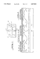
- FIG. 1 is a top plan view of a typical MOSGATE control device and illustrates connection pads on the top surface of the device.
- FIG. 2 is a cross-section of a small portion of the device of FIG. 1 to illustrate the cellular construction employed in the device for an IGBT type of structure.
- FIG. 3 is a cross-sectional view of FIG. 1 taken across the section lines 3--3 and illustrates an intermediate stage in the process of forming a solderable electrode pad on the front of the chip.
- FIG. 4 is similar to FIG. 3 and shows the solder pad in place with a relatively massive lead connected to the solder pad.
- a chip 10 which may be an insulated gate bipolar transistor (IGBT).
- the device is a vertical conduction device and has a main electrode pad 11 on its upper surface and a gate or control electrode pad 12 also on its upper surface but separated from and insulated from the main electrode pad 11.
- the bottom surface of the chip 10 receives the other main electrode of the device.
- FIG. 2 is a cross-section of the region A of FIG. 1 to illustrate the cellular nature of the junctions at the top surface of the chip IGBT device.
- FIG. 2 also shows the device at an intermediate stage of its manufacture.
- the MOSGATE junctions can exist beneath the front contact pad area because they are not exposed to pressure damage during lead attachment when using the solderable contact of the invention.
- FIG. 2 The basic process for the manufacture of the junction patterns in the device shown in FIG. 2 is that disclosed in U.S. Pat. No. 4,593,302 which is assigned to the assignee of the present invention. That patent, however, shows a power MOSFET structure whereas FIG. 2 is a pattern for an IGBT so that the substrate in FIG. 2 is the P+ substrate 20 upon which the N(-) epitaxial layer 21 is grown.
- the processing for forming the cell structures in the epitaxial layer 21 can be that disclosed in the above-noted patent.
- the several cells shown in FIG. 2 are hexagonal in topology.
- the chip 10 of FIG. 1 may be of the size of a HEX3 chip, sold by the assignee of this invention, and has tens of thousands of such cells distributed over its full surface.
- Each of these cells consists of a body region 22 which has a central deepened P+ region and an outer lower conductivity P-type region defining the channel region for the device.
- Each of the P-type regions 22 receives an annular source 23 which is of the N+ conductivity for the N channel device shown in FIG. 2. Note that the conductivity types can be reversed if a P channel device is desired.
- a grid or lattice of gate oxide is deposited over the surface of the device, with a few gate oxide strips 30 being visible in FIG. 2. These gate oxide strips 30 are covered with conductive polysilicon gate strips 31 which overlie the P-type channels within each of the bodies 22. The entire lattice of polysilicon gate strips 31 is electrically interconnected.
- the gate lattice within the device is covered by a silicon dioxide insulation coating 40 which is appropriately patterned and then covered with an aluminum layer 41 which makes contact to the source regions 23 and to the central of the P+ hexagonal body regions.
- Aluminum layer 41 is relatively thin, for example, from 1 micron to 4 microns. A thicker aluminum layer cannot be used because of the difficulty of etching fine patterns in such thick aluminum.
- Aluminum layer 41 is also arranged to define a gate pad in contact with the polysilicon gate 31.
- solderable metal 42 is next deposited atop the aluminum layer 41. This process may take place on the full wafer before chips or die are separated from the wafer.
- a preferred solderable metal is a tri-metal 42 consisting of layers of titanium, palladium and silver.
- the titanium, palladium and silver layers are formed by sequential evaporation although other techniques can be used.
- the titanium layer is deposited atop the aluminum 41 to a thickness of about 1,000 Angstroms.
- the palladium layer is deposited atop the titanium to a thickness of about 3,000 Angstroms.
- the silver layer is deposited atop the palladium and may have a thickness from about 3,000 Angstroms to about 15,000 Angstroms.
- solderable metal systems can be used in place of the tri-metal 42.
- a nickel layer about 3,000 Angstroms thick, can first be deposited atop the aluminum layer 41 in FIG. 2.
- a gold layer from 500 to 1,000 Angstroms is then formed atop the nickel.
- the gold layer is easily solderable as is the silver layer of the tri-metal layer 42 previously described.
- the entire wafer is masked and the tri-metal and aluminum surfaces are patterned, etched and passivated as desired, exposing the gate pad and the solderable main electrode pad.
- a coating of amorphous silicon 50 is then applied over the entire surface of the wafer in FIG. 3 to a thickness of about 1,200 Angstroms.
- the coating 50 is then covered with a photo-polyimide layer which can be spun to a thickness of 2 to 3 microns.
- the wafer is then etched as by an appropriate plasma etch to open the window for gate pad 12 in FIG. 3 and window for the main electrode pad 11 in FIG. 3.
- the amorphous silicon is employed as a termination structure for the high voltage structure.
- the photo-polyimide is used as a mask medium and as a hermetic seal over the amorphous silicon termination.
- the amorphous silicon is cut short of the solderable metal 42 and overlaps only the aluminum layer 41. This is done particularly where the solderable metal is terminated with gold since the gold on silicon will melt at about 370° C. which is somewhat lower than the temperature at which the photo-polyimide is imidized or cross-linked.
- the wafer is subjected to a wet etch, for example, in a de-freckling etch consisting of CF4 plus oxygen. This etch removes scum on the silver at the upper surface of layer 42 in FIG. 3.
- the photo-polyimide layer 51 is imidized.
- the wafer is heated to 420° C. for about 30 minutes in an atmosphere of a hydrogen and nitrogen gas mixture. Thereafter, the wafer is exposed to a 1 to 1 nitric acid and water mixture at 50° C. for about 15 seconds to remove scum from the exposed silver in the tri-metal layer 42. The wafer is then rinsed and baked dry.
- a suitable back metal which may consist of a chrome-nickel-silver layer 60 in FIG. 3, is applied to the back surface of the wafer by any conventional process such as that described in the aforementioned U.S. Pat. No. 4,593,302.
- solder-clad molybdenum or tungsten preform can be used.
- the preform can be a single wafer with severable segments adapted for soldering to each of the front main electrode pads of each chip within the wafer and severed when the wafer is separated into individual chips.
- preform chips can be applied to individual device chips after separation of the wafer.
- a pure solder preform of wafer or chip size and 30 to 40 microns thick may be placed in registry with the main electrode area in pad 11 and between solderable layer 42 and the solder-clad preform.
- the preform may be 10 mils thick.
- the assembly may then be placed in a solder oven and heated to cause the solder preform and the solder-clad refractory metal preform to solder together with the upper surface of the solderable tri-metal 42.
- solder material can be used for the solder preform and solder cladding.
- a lead-indium-silver solder or any similar soft solder can be used.
- the solder will not wet the amorphous silicon 50 and, therefore, the solder of the solder mass shown as the solder mass 70 in FIG. 4 cannot flow into contact with the gate contact 12.
- the bottom electrode 60 may be soldered to the heat sink portion of a lead frame and gate and main electrode leads are connected to the gate pad and solderable main electrode pad on the front surface of the chip.
- a relatively large heat conductive lead 80 can be soldered to the solder mass 70 in FIG. 4.
- the lead 80 as contrasted to a thin, fragile bonded lead wire used for the gate, is a robust wire of copper or silver, preferably solder-clad as by plating with nickel and gold. This lead can then remove considerable heat from the front surface of the chip to an external massive heat sink as compared to the small amount of heat which is transferred through a prior art pressure-bonded lead to the aluminum contact pad.
- the gate is not a high current carrying structure, the solderable terminal need not be applied to the gate structure and a simple gate lead 81 can be conventionally bonded to the gate bonding pad in the usual manner.
Abstract
Description
Claims (9)
Priority Applications (1)
| Application Number | Priority Date | Filing Date | Title |
|---|---|---|---|
| US07/599,148 US5047833A (en) | 1990-10-17 | 1990-10-17 | Solderable front metal contact for MOS devices |
Applications Claiming Priority (1)
| Application Number | Priority Date | Filing Date | Title |
|---|---|---|---|
| US07/599,148 US5047833A (en) | 1990-10-17 | 1990-10-17 | Solderable front metal contact for MOS devices |
Publications (1)
| Publication Number | Publication Date |
|---|---|
| US5047833A true US5047833A (en) | 1991-09-10 |
Family
ID=24398439
Family Applications (1)
| Application Number | Title | Priority Date | Filing Date |
|---|---|---|---|
| US07/599,148 Expired - Lifetime US5047833A (en) | 1990-10-17 | 1990-10-17 | Solderable front metal contact for MOS devices |
Country Status (1)
| Country | Link |
|---|---|
| US (1) | US5047833A (en) |
Cited By (23)
| Publication number | Priority date | Publication date | Assignee | Title |
|---|---|---|---|---|
| US5473181A (en) * | 1993-11-05 | 1995-12-05 | Siemens Aktiengesellschaft | Integrated circuit arrangement having at least one power component and low-voltage components |
| US5592026A (en) * | 1993-12-24 | 1997-01-07 | Consorzio Per La Ricerca Sulla Microelettronica Nel Mezzogiorno | Integrated structure pad assembly for lead bonding |
| US5631476A (en) * | 1994-08-02 | 1997-05-20 | Sgs-Thomson Microelectronics S.R.L. | MOS-technology power device chip and package assembly |
| US5798287A (en) * | 1993-12-24 | 1998-08-25 | Consorzio Per La Ricerca Sulla Microelettronica Nel Mezzogiorno | Method for forming a power MOS device chip |
| US5821616A (en) * | 1993-12-24 | 1998-10-13 | Consorzio Per La Ricerca Sulla Microelettronica Nel Mezzogiorno | Power MOS device chip and package assembly |
| US5883412A (en) * | 1994-07-14 | 1999-03-16 | Sgs-Thomson Microelectronics S.R.L. | Low gate resistance high-speed MOS-technology integrated structure |
| US6164523A (en) * | 1998-07-01 | 2000-12-26 | Semiconductor Components Industries, Llc | Electronic component and method of manufacture |
| US6222232B1 (en) | 1996-07-05 | 2001-04-24 | Sgs-Thomson Microelectronics S.R.L. | Asymmetric MOS technology power device |
| US6246583B1 (en) | 1999-03-04 | 2001-06-12 | International Business Machines Corporation | Method and apparatus for removing heat from a semiconductor device |
| WO2001075961A1 (en) * | 2000-04-04 | 2001-10-11 | International Rectifier Corporation | Chip scale surface mounted device and process of manufacture |
| WO2003060984A1 (en) * | 2001-12-21 | 2003-07-24 | International Rectifier Corporation | Surface mounted package with die bottom spaced from support board |
| US6781203B2 (en) * | 2001-11-09 | 2004-08-24 | International Rectifier Corporation | MOSFET with reduced threshold voltage and on resistance and process for its manufacture |
| US20060086939A1 (en) * | 2004-10-21 | 2006-04-27 | International Rectifier Corp. | Solderable top metal for SiC device |
| US20060197105A1 (en) * | 2005-03-04 | 2006-09-07 | Rossano Carta | Power semiconductor switch |
| US20060214242A1 (en) * | 2005-03-04 | 2006-09-28 | International Rectifier Corporation | Termination for SiC trench devices |
| US20060281315A1 (en) * | 2005-06-08 | 2006-12-14 | International Rectifier Corporation | Process of manufacture of ultra thin semiconductor wafers with bonded conductive hard carrier |
| US20070090481A1 (en) * | 2005-10-20 | 2007-04-26 | International Rectifier Corporation | Silicon carbide schottky diode |
| US20080093729A1 (en) * | 2006-10-20 | 2008-04-24 | Dirk Siepe | Semiconductor arrangement, semiconductor module, and method for connecting a semiconductor chip to a ceramic substrate |
| US20080237608A1 (en) * | 2006-07-31 | 2008-10-02 | Giovanni Richieri | Molybdenum barrier metal for SiC Schottky diode and process of manufacture |
| US20090218684A1 (en) * | 2008-01-25 | 2009-09-03 | Mark Pavier | Autoclave capable chip-scale package |
| US20100210088A1 (en) * | 2009-02-19 | 2010-08-19 | Sony Corporation | Manufacturing method of semiconductor device |
| US9412880B2 (en) | 2004-10-21 | 2016-08-09 | Vishay-Siliconix | Schottky diode with improved surge capability |
| US11063495B2 (en) | 2019-07-01 | 2021-07-13 | Nidec Motor Corporation | Heatsink clamp for multiple electronic components |
Citations (4)
| Publication number | Priority date | Publication date | Assignee | Title |
|---|---|---|---|---|
| US4593302A (en) * | 1980-08-18 | 1986-06-03 | International Rectifier Corporation | Process for manufacture of high power MOSFET with laterally distributed high carrier density beneath the gate oxide |
| US4635091A (en) * | 1983-08-17 | 1987-01-06 | U.S. Philips Corporation | Semiconductor device having overload protection |
| US4742380A (en) * | 1982-02-09 | 1988-05-03 | American Telephone And Telegraph Company, At&T Bell Laboratories | Switch utilizing solid-state relay |
| US4796084A (en) * | 1985-05-13 | 1989-01-03 | Kabushiki Kaisha Toshiba | Semiconductor device having high resistance to electrostatic and electromagnetic induction using a complementary shield pattern |
-
1990
- 1990-10-17 US US07/599,148 patent/US5047833A/en not_active Expired - Lifetime
Patent Citations (5)
| Publication number | Priority date | Publication date | Assignee | Title |
|---|---|---|---|---|
| US4593302A (en) * | 1980-08-18 | 1986-06-03 | International Rectifier Corporation | Process for manufacture of high power MOSFET with laterally distributed high carrier density beneath the gate oxide |
| US4593302B1 (en) * | 1980-08-18 | 1998-02-03 | Int Rectifier Corp | Process for manufacture of high power mosfet laterally distributed high carrier density beneath the gate oxide |
| US4742380A (en) * | 1982-02-09 | 1988-05-03 | American Telephone And Telegraph Company, At&T Bell Laboratories | Switch utilizing solid-state relay |
| US4635091A (en) * | 1983-08-17 | 1987-01-06 | U.S. Philips Corporation | Semiconductor device having overload protection |
| US4796084A (en) * | 1985-05-13 | 1989-01-03 | Kabushiki Kaisha Toshiba | Semiconductor device having high resistance to electrostatic and electromagnetic induction using a complementary shield pattern |
Cited By (60)
| Publication number | Priority date | Publication date | Assignee | Title |
|---|---|---|---|---|
| US5473181A (en) * | 1993-11-05 | 1995-12-05 | Siemens Aktiengesellschaft | Integrated circuit arrangement having at least one power component and low-voltage components |
| US5888889A (en) * | 1993-12-24 | 1999-03-30 | Consorzio Per La Ricerca Sulla Microelettronica Nel Mezzogiorno | Integrated structure pad assembly for lead bonding |
| US5592026A (en) * | 1993-12-24 | 1997-01-07 | Consorzio Per La Ricerca Sulla Microelettronica Nel Mezzogiorno | Integrated structure pad assembly for lead bonding |
| US5798287A (en) * | 1993-12-24 | 1998-08-25 | Consorzio Per La Ricerca Sulla Microelettronica Nel Mezzogiorno | Method for forming a power MOS device chip |
| US5821616A (en) * | 1993-12-24 | 1998-10-13 | Consorzio Per La Ricerca Sulla Microelettronica Nel Mezzogiorno | Power MOS device chip and package assembly |
| US5883412A (en) * | 1994-07-14 | 1999-03-16 | Sgs-Thomson Microelectronics S.R.L. | Low gate resistance high-speed MOS-technology integrated structure |
| US5933734A (en) * | 1994-07-14 | 1999-08-03 | Sgs-Thomson Microelectronics S.R.L. | High speed MOS-technology power device integrated structure, and related manufacturing process |
| US5851855A (en) * | 1994-08-02 | 1998-12-22 | Sgs-Thomson Microelectronics S.R.L. | Process for manufacturing a MOS-technology power device chip and package assembly |
| US5631476A (en) * | 1994-08-02 | 1997-05-20 | Sgs-Thomson Microelectronics S.R.L. | MOS-technology power device chip and package assembly |
| US6326271B2 (en) | 1996-07-05 | 2001-12-04 | Sgs-Thomson Microelectronics S.R.L. | Asymmetric MOS technology power device |
| US6222232B1 (en) | 1996-07-05 | 2001-04-24 | Sgs-Thomson Microelectronics S.R.L. | Asymmetric MOS technology power device |
| US6164523A (en) * | 1998-07-01 | 2000-12-26 | Semiconductor Components Industries, Llc | Electronic component and method of manufacture |
| US6246583B1 (en) | 1999-03-04 | 2001-06-12 | International Business Machines Corporation | Method and apparatus for removing heat from a semiconductor device |
| US6767820B2 (en) * | 2000-04-04 | 2004-07-27 | International Rectifier Corporation | Chip scale surface mounted device and process of manufacture |
| CN1316577C (en) * | 2000-04-04 | 2007-05-16 | 国际整流器公司 | Chip scale surface mounted device and its process of manufacture |
| US6624522B2 (en) | 2000-04-04 | 2003-09-23 | International Rectifier Corporation | Chip scale surface mounted device and process of manufacture |
| US20040026796A1 (en) * | 2000-04-04 | 2004-02-12 | International Rectifier Corporation | Chip scale surface mounted device and process of manufacture |
| US20040038509A1 (en) * | 2000-04-04 | 2004-02-26 | International Rectifier Corporation | Chip scale surface mounted device and process of manufacture |
| US7476979B2 (en) | 2000-04-04 | 2009-01-13 | International Rectifier Corporation | Chip scale surface mounted device and process of manufacture |
| US7253090B2 (en) | 2000-04-04 | 2007-08-07 | International Rectifier Corporation | Chip scale surface mounted device and process of manufacture |
| US20040224438A1 (en) * | 2000-04-04 | 2004-11-11 | International Rectifier Corporation | Chip scale surface mounted device and process of manufacture |
| US6890845B2 (en) | 2000-04-04 | 2005-05-10 | International Rectifier Corporation | Chip scale surface mounted device and process of manufacture |
| WO2001075961A1 (en) * | 2000-04-04 | 2001-10-11 | International Rectifier Corporation | Chip scale surface mounted device and process of manufacture |
| US20050186707A1 (en) * | 2000-04-04 | 2005-08-25 | International Rectifier Corp. | Chip scale surface mounted device and process of manufacture |
| US7122887B2 (en) | 2000-04-04 | 2006-10-17 | International Rectifier Corporation | Chip scale surface mounted device and process of manufacture |
| US20060220123A1 (en) * | 2000-04-04 | 2006-10-05 | International Rectifier Corporation | Chip scale surface mounted device and process of manufacture |
| US7285866B2 (en) | 2001-03-28 | 2007-10-23 | International Rectifier Corporation | Surface mounted package with die bottom spaced from support board |
| US20050224960A1 (en) * | 2001-03-28 | 2005-10-13 | International Rectifier Corporation | Surface mounted package with die bottom spaced from support board |
| US6930397B2 (en) | 2001-03-28 | 2005-08-16 | International Rectifier Corporation | Surface mounted package with die bottom spaced from support board |
| US6781203B2 (en) * | 2001-11-09 | 2004-08-24 | International Rectifier Corporation | MOSFET with reduced threshold voltage and on resistance and process for its manufacture |
| WO2003060984A1 (en) * | 2001-12-21 | 2003-07-24 | International Rectifier Corporation | Surface mounted package with die bottom spaced from support board |
| US9412880B2 (en) | 2004-10-21 | 2016-08-09 | Vishay-Siliconix | Schottky diode with improved surge capability |
| US20060086939A1 (en) * | 2004-10-21 | 2006-04-27 | International Rectifier Corp. | Solderable top metal for SiC device |
| EP1810338A4 (en) * | 2004-10-21 | 2011-02-23 | Siliconix Technology C V | Solderable top metal for sic device |
| EP1810338A2 (en) * | 2004-10-21 | 2007-07-25 | International Rectifier Corporation | Solderable top metal for sic device |
| US9496421B2 (en) * | 2004-10-21 | 2016-11-15 | Siliconix Technology C.V. | Solderable top metal for silicon carbide semiconductor devices |
| US20080286968A1 (en) * | 2004-10-21 | 2008-11-20 | Siliconix Technology C.V. | Solderable top metal for silicon carbide semiconductor devices |
| JP2008518445A (en) * | 2004-10-21 | 2008-05-29 | インターナショナル レクティファイアー コーポレイション | Solderable top metal for silicon carbide devices |
| US7394158B2 (en) * | 2004-10-21 | 2008-07-01 | Siliconix Technology C.V. | Solderable top metal for SiC device |
| US7834376B2 (en) | 2005-03-04 | 2010-11-16 | Siliconix Technology C. V. | Power semiconductor switch |
| US20060197105A1 (en) * | 2005-03-04 | 2006-09-07 | Rossano Carta | Power semiconductor switch |
| US9472403B2 (en) | 2005-03-04 | 2016-10-18 | Siliconix Technology C.V. | Power semiconductor switch with plurality of trenches |
| US9419092B2 (en) | 2005-03-04 | 2016-08-16 | Vishay-Siliconix | Termination for SiC trench devices |
| US20060214242A1 (en) * | 2005-03-04 | 2006-09-28 | International Rectifier Corporation | Termination for SiC trench devices |
| US20060281315A1 (en) * | 2005-06-08 | 2006-12-14 | International Rectifier Corporation | Process of manufacture of ultra thin semiconductor wafers with bonded conductive hard carrier |
| US7682935B2 (en) * | 2005-06-08 | 2010-03-23 | International Rectifier Corporation | Process of manufacture of ultra thin semiconductor wafers with bonded conductive hard carrier |
| US20070090481A1 (en) * | 2005-10-20 | 2007-04-26 | International Rectifier Corporation | Silicon carbide schottky diode |
| US8368165B2 (en) | 2005-10-20 | 2013-02-05 | Siliconix Technology C. V. | Silicon carbide Schottky diode |
| US9627553B2 (en) | 2005-10-20 | 2017-04-18 | Siliconix Technology C.V. | Silicon carbide schottky diode |
| US9627552B2 (en) | 2006-07-31 | 2017-04-18 | Vishay-Siliconix | Molybdenum barrier metal for SiC Schottky diode and process of manufacture |
| US20080237608A1 (en) * | 2006-07-31 | 2008-10-02 | Giovanni Richieri | Molybdenum barrier metal for SiC Schottky diode and process of manufacture |
| US20080093729A1 (en) * | 2006-10-20 | 2008-04-24 | Dirk Siepe | Semiconductor arrangement, semiconductor module, and method for connecting a semiconductor chip to a ceramic substrate |
| DE102007046021C5 (en) * | 2006-10-20 | 2016-07-14 | Infineon Technologies Ag | Method for connecting a semiconductor chip to a ceramic substrate |
| DE102007046021B4 (en) * | 2006-10-20 | 2012-09-13 | Infineon Technologies Ag | A semiconductor device, semiconductor module and method for connecting a semiconductor chip to a ceramic substrate |
| US8164176B2 (en) | 2006-10-20 | 2012-04-24 | Infineon Technologies Ag | Semiconductor module arrangement |
| US20090218684A1 (en) * | 2008-01-25 | 2009-09-03 | Mark Pavier | Autoclave capable chip-scale package |
| US8143729B2 (en) * | 2008-01-25 | 2012-03-27 | International Rectifier Corporation | Autoclave capable chip-scale package |
| US8361876B2 (en) * | 2009-02-19 | 2013-01-29 | Sony Corporation | Manufacturing method of semiconductor device |
| US20100210088A1 (en) * | 2009-02-19 | 2010-08-19 | Sony Corporation | Manufacturing method of semiconductor device |
| US11063495B2 (en) | 2019-07-01 | 2021-07-13 | Nidec Motor Corporation | Heatsink clamp for multiple electronic components |
Similar Documents
| Publication | Publication Date | Title |
|---|---|---|
| US5047833A (en) | Solderable front metal contact for MOS devices | |
| US7394158B2 (en) | Solderable top metal for SiC device | |
| US5915179A (en) | Semiconductor device and method of manufacturing the same | |
| US8169063B2 (en) | Semiconductor component and method for producing the same | |
| TWI395277B (en) | Wafer level chip scale packaging | |
| US4996586A (en) | Crimp-type semiconductor device having non-alloy structure | |
| JPH07183302A (en) | Formation of metal layer and bonding method therefor | |
| EP0018175B1 (en) | Process for producing an electrode on a semiconductor device | |
| US3349297A (en) | Surface barrier semiconductor translating device | |
| US7368380B2 (en) | Method of manufacturing semiconductor device | |
| JPH10163467A (en) | Semiconductor device and formation of electrode | |
| US20210257274A1 (en) | Semiconductor element and semiconductor device | |
| JP2552100B2 (en) | Integrated structure pad assembly and manufacturing method thereof | |
| JP3432708B2 (en) | Semiconductor devices and semiconductor modules | |
| US4695869A (en) | GAAS semiconductor device | |
| JP2005079462A (en) | Semiconductor device and method for manufacturing the same | |
| GB2095904A (en) | Semiconductor device with built-up low resistance contact and laterally conducting second contact | |
| JP2001044414A (en) | Semiconductor device | |
| US3840982A (en) | Contacts for semiconductor devices, particularly integrated circuits, and methods of making the same | |
| JPS609159A (en) | Semiconductor device | |
| JPH04293268A (en) | Semiconductor device and manufacture thereof | |
| CN114467165A (en) | Semiconductor device with a plurality of semiconductor chips | |
| JPH06296012A (en) | Semiconductor device and its manufacture | |
| JP2756826B2 (en) | Semiconductor device and manufacturing method thereof | |
| US4320571A (en) | Stencil mask process for high power, high speed controlled rectifiers |
Legal Events
| Date | Code | Title | Description |
|---|---|---|---|
| AS | Assignment |
Owner name: INTERNATIONAL RECTIFIER CORPORATION, A CORP. OF DE Free format text: ASSIGNMENT OF ASSIGNORS INTEREST.;ASSIGNOR:GOULD, HERBERT J.;REEL/FRAME:005479/0491 Effective date: 19900919 |
|
| STCF | Information on status: patent grant |
Free format text: PATENTED CASE |
|
| FEPP | Fee payment procedure |
Free format text: PAYOR NUMBER ASSIGNED (ORIGINAL EVENT CODE: ASPN); ENTITY STATUS OF PATENT OWNER: LARGE ENTITY |
|
| FPAY | Fee payment |
Year of fee payment: 4 |
|
| FPAY | Fee payment |
Year of fee payment: 8 |
|
| AS | Assignment |
Owner name: BANQUE NATIONALE DE PARIS, CALIFORNIA Free format text: SECURITY INTEREST;ASSIGNOR:INTERNATIONAL RECTIFIER CORP.;REEL/FRAME:010070/0701 Effective date: 19990711 |
|
| FPAY | Fee payment |
Year of fee payment: 12 |