US5016261A - Method and apparatus for achieving improved anti-jam performance via conversion gain - Google Patents
Method and apparatus for achieving improved anti-jam performance via conversion gain Download PDFInfo
- Publication number
- US5016261A US5016261A US07/339,552 US33955289A US5016261A US 5016261 A US5016261 A US 5016261A US 33955289 A US33955289 A US 33955289A US 5016261 A US5016261 A US 5016261A
- Authority
- US
- United States
- Prior art keywords
- signal
- chips
- gain factor
- interference
- amplitude
- Prior art date
- Legal status (The legal status is an assumption and is not a legal conclusion. Google has not performed a legal analysis and makes no representation as to the accuracy of the status listed.)
- Expired - Fee Related
Links
Images


Classifications
-
- H—ELECTRICITY
- H04—ELECTRIC COMMUNICATION TECHNIQUE
- H04B—TRANSMISSION
- H04B7/00—Radio transmission systems, i.e. using radiation field
- H04B7/14—Relay systems
- H04B7/15—Active relay systems
-
- H—ELECTRICITY
- H04—ELECTRIC COMMUNICATION TECHNIQUE
- H04B—TRANSMISSION
- H04B1/00—Details of transmission systems, not covered by a single one of groups H04B3/00 - H04B13/00; Details of transmission systems not characterised by the medium used for transmission
- H04B1/69—Spread spectrum techniques
- H04B1/707—Spread spectrum techniques using direct sequence modulation
- H04B1/709—Correlator structure
- H04B1/7093—Matched filter type
-
- H—ELECTRICITY
- H04—ELECTRIC COMMUNICATION TECHNIQUE
- H04K—SECRET COMMUNICATION; JAMMING OF COMMUNICATION
- H04K3/00—Jamming of communication; Counter-measures
- H04K3/20—Countermeasures against jamming
- H04K3/22—Countermeasures against jamming including jamming detection and monitoring
- H04K3/224—Countermeasures against jamming including jamming detection and monitoring with countermeasures at transmission and/or reception of the jammed signal, e.g. stopping operation of transmitter or receiver, nulling or enhancing transmitted power in direction of or at frequency of jammer
- H04K3/228—Elimination in the received signal of jamming or of data corrupted by jamming
Definitions
- the present invention relates generally to radio communications systems and more particularly to the optimized rejection of electronic carrier wave (CW) interference in phase modulated, phase noncoherent radio signals including direct sequence pseudonoise signals such as those used in the Joint Tactical Distribution System (JTIDS) signals.
- CW electronic carrier wave
- JTIDS Joint Tactical Distribution System
- Time Division Multiple Access (TDMA) radio communication systems provide integrated communication, navigation, identification and position location means for military operations.
- TDMA Time Division Multiple Access
- Tactical radio communications in an electronic warfare (EW) environment must be made as immune as possible from all EW measures such as high power brute force jammers, spoof jammers, electronic signal interceptors, and direction finders. Simply increasing friendly transmitter power is expensive as well as ineffective against spoof jammers, interceptors, and direction finders.
- TDMA Time Division Multiple Access
- JTIDS jam resistant, intercept-resistant phase modulated, phase noncoherent spread spectrum Direct Sequence Pseudonoise (DSPN) communication links such as Joint Tactical Information Distribution System (JTIDS) have been developed for TDMA communications.
- DSPN spread spectrum Direct Sequence Pseudonoise
- JTIDS is a notable example of a communications system which utilizes a phase modulated, phase noncoherent radio signal with antijam capabilities.
- JTIDS is an integrated communications, navigation, and identification TDMA military communications system designed to operate in a 960-1215 MHz TACAN band and in a CW tactical environment spanning a geographic area of up to 500 miles.
- the time division JTIDS architecture allows multiple users to participate in the communications network.
- the various terminals of the JTIDS network may comprise, for example, mission aircraft subscribers, sea based subscribers and ground subscribers. All terminals in the network can listen to all time divisions or time slots in which they are not transmitting. Code division mulitiplexing is used to provide multiple communication networks which have overlapping coverage patterns.
- a terminal can switch between multiple networks on a time slot by time slot basis.
- Each 7.8125 millisecond time slot contains a 3354-microsecond transmission burst comprising 129 symbols, each symbol having a duration of 26 microseconds. Symbols consist of either one or two 32-chip pulses, each of a duration of 6.4 microseconds.
- the TDMA signal is currently processed by an MSK chip matched filter followed by an IAGC, such as the MITRE IAGC, which may be viewed as a hard limiter followed by a three bit phase quantizer.
- the phase quantizer is followed by a signal correlator, which in the JTIDS processor comprises a 32 chip pulse correlator.
- the DSPN information signal plus CW and Gaussian interference signal enter the chip matched filter at a jammer power to signal power ratio of J/S.
- the chip matched filter serves to maximize the ratio of signal power to the Gaussian component of interference.
- the MITRE IAGC provides the signal processing with a property called constant false alarm rate (CFAR) wherein any sudden high power burst of spurious jamming or noise entering the system will be clipped to a preset amplitude level and thereby prevented from propagating further into the chain of signal processors.
- CFAR constant false alarm rate
- the probability of declaring a noise symbol to be a signal symbol remains constant, independent of the magnitude of that high power burst of jamming.
- Hard limiting also introduces what is known as a small signal suppression effect which degrades the signal to noise ratio of the signal entering the correlator.
- the noise equivalent bandwidth of the chip matched filter is a fraction .sup. ⁇ 2 /16, of the chip rate or 0.62 times the chip rate, which is equivalent to -2.1 dB. Consequently, J/S increases by 2.1 dB as the input signal together with a band-centered CW jammer pass through the matched filter.
- the effects of small signal suppression in the hard limiter result in a further increase in J/S of about 4.3 dB (greater than 4.3 dB if J/S at the hard limiter input is greater than 2.1 dB).
- J/S conversion loss in the order of 4.3 dB represents a 2.7 to 1 loss in relation to transmitter power, it constitutes a substantial deficiency in JTIDS and other phase modulated, phase noncoherent signal processing systems not heretofore adequately addressed in the prior art.
- Input segments are each segregated into signal chips, sorted by magnitude and separated in accordance with a predetermined threshold.
- the threshold is repeatedly reset to distinguish a predetermined number of signals chips having greater magnitudes.
- the threshold level may, therefore, vary in accordance with the particular signal chips forming each input segment.
- a first weighting gain factor is applied to signal chips whose magnitudes equal or exceed the threshold, and a second weighting gain factor is applied to the remaining chips, the first weighting gain factor being greater than the second weighting gain factor.
- a flash converter is used to sort signal chips, in accordance with amplitude, and to determine which of the signal chips have greater magnitude.
- the received signals are each segregated into 32 signal chips.
- the first threshold and weighting gain factor are set to optimize conversion gain in the presence of CW interference, without sacrificing conversion gain in the presence of Gaussian interference. Determination of the optimum threshold level and weighting gain factor may be determined experimentally or by mathematical modeling. Experimental determination proceeds by first assuming a characteristic signal-to-noise ratio for the received signal, selecting a preliminary amplitude threshold for evaluation and varying the preliminary amplitude threshold and weighting gain factor to determine the characteristic gain of the circuit in the presence of continuous CW interference. A threshold amplitude level and weighting gain factor may then be identified that provide optimum performance with respect to CW interference.
- the performance of the circuit may then be evaluated with respect to Gaussian interference, and the results compared with the performance of a hard limiter in the presence of the same Gaussian interference.
- the identified amplitude threshold level may then be adjusted to ensure that the performance of the circuit under Gaussian noise conditions is at least as favorable as the performance of a hard limiter under such conditions. Though performance of the circuit in the presence of CW interference may thus be slightly reduced, the performance remains superior to contemporary systems.
- the optimum gain factor was determined to be 8
- the optimum amplitude threshold level, with respect to CW interference alone was determined to be approximately 60%
- the optimum compromise amplitude threshold level with respect to both CW interference and Gaussian interference was determined to be approximately 70%.
- the circuit preferably operates to repeatedly sort the received signal chips in order of amplitude and to apply a gain factor of 8 to those chips appearing in the top 70 percentile by amplitude. The remaining chips are not so amplified, i.e. a gain factor of 1 is applied.
- the circuit has been found effective with respect to both constant power CW interference and pulsed CW interference, as described more fully below.
- FIG. 1a is a block diagram illustrating the sequence of signal processing steps in a contemporary JTIDS system
- FIG. 1b is a block diagram illustrating a sequence of signal processing steps in accordance with the present invention.
- FIG. 2 illustrates the operation of a contemporary hard limiter within a JTIDS signal format, in polar coordinates
- FIG. 3 illustrates the operation of the present invention in the same format as FIG. 2;
- FIG. 4 further illustrates the operation of the present invention including the use of a weighting gain factor
- FIG. 5 illustrates the effective distribution of points representing signal chips after the application of a weighting gain factor and phase quantization as in the contemporary MITRE IAGC;
- FIG. 6 illustrates the family of conversion gain curves for varying weighting gain factors for continuous CW interference
- FIG. 7 compares hard limiter behavior under different circumstances to the adaptive converter of the present invention with different weighting gain factors, again in continuous CW interference;
- FIG. 8 illustrates the conversion gain of the present invention, at a set weighting gain factor, in the presence of Gaussian interference
- FIG. 9 illustrates conversion gain of the present invention in a pulsed jamming environment as a function of the number of chips jammed
- FIG. 10 repeats the analysis of FIG. 9 for a different signal-to-noise ratio
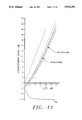
- FIG. 11 illustrates the conversion gain for continuous CW jamming at different signal-to-noise ratios
- FIG. 12 illustrates a comparison of the present invention with alternative models for processing the signal chips, including existing systems, all in a pulse jamming environment;
- FIG. 13a, 13b and 13c illustrate mathematical analyses relating to determining the optimum threshold level in Gaussian noise
- FIG. 14 is a flow chart illustrating an approximate mathematical analysis of the present invention.
- FIG. 1a illustrates the sequence of signal processing steps for a contemporary JTIDS system.
- the information plus interference signals enter the chip matched filter at the IF input 21. At that location the ratio of jammer power to signal power is identified as (J/S) 1 .
- the matched filter 23 is assumed to be normalized to unit energy impulse response, and the jammer frequency, as before, is assumed to be centered on the IF frequency.
- Contemporary IAGC 25 action may be viewed as a combination of a hard limiter 27 followed by a 3-bit phase quantizer 29 that assigns one of 8 phase states.
- the output of the IAGC 25 is communicated to a 32 chip pulse correlator 31.
- the output of the pulse correlator 31 is then communicated to additional processing circuitry (not shown) which accumulates and interprets the signal from the correlator.
- the present invention is distinguishable from such contemporary systems by the use of an adaptive A/D multilevel quantizer, as illustrated in FIG. 1b.
- the function of the adaptive A/D converter 11 is to assign an amplitude value, either HIGH or LOW to each chip. That amplitude value, determined by adaptive threshold circuit 13, along with signal chip phase information extracted by phase correlator 29, is communicated to the 32 chip pulse correlator 15 in such a manner as to increase the weight given to the phase information extracted from chips having high magnitude.
- the A/D converter 11 is constructed to be able to accumulate and sort a plurality of chips, e.g. 32 chips received during an output signal segment.
- the chips are sorted in accordance with their magnitude, and a threshold is set in order to distinguish chips having a lower magnitude from chips having a higher magnitude.
- a threshold is set in order to distinguish chips having a lower magnitude from chips having a higher magnitude.
- the higher magnitude chips are more likely to be characterized by a higher ratio of information signal-to-interference signal.
- the circuit operates to emphasize the chips likely to have a greater information signal content, i.e. more reliable phase angle information.
- Further signal processing (not shown) operates to aggregate the information from the circuit to extract the necessary information. By emphasizing chips that generally convey correct phase information the function of such additional signal processing is rendered more reliable.
- the threshold level for the A/D converter is set is described more fully below.
- the threshold level and weighting factor are optimized to produce the highest conversion gain, assuming a CW interference signal and a characteristic signal to noise ratio of the input signal.
- the performance of such a circuit, optimized for CW interference is then evaluated for Gaussian noise conditions.
- the optimum threshold level may then be adjusted such that the performance of the circuit in Gaussian noise conditions at least equals the performance of a hard limiter (without the adaptive A/D converter) under similar Gaussian noise conditions.
- a determination of the optimum amplitude threshold and weighting factor may be effected for both continuous CW interference and pulsed CW interference.
- FIG. 2 illustrates how a hard limiter operates within the JTIDS signal format, in polar coordinates.
- FIG. 3 illustrates how the A/D converter of the present invention operates in the same format.
- the signal chip A is assigned unit magnitude and zero phase. Because JTIDS detection is noncoherent the signal processing will take no account of the static difference between the phase of the received carrier and that of the locally supplied carrier. Instead, the phase angles of all chips will be measured relative to each other.
- Added to the typical signal chip is an interference vector B, with phase .sup. ⁇ B relative to A. In the present step of analysis the vector B will have a constant magnitude to represent constant CW interference. In general, the phase of B will vary with respect to the signal vector.
- the ⁇ B will increase at the rate 2 ⁇ f radians/second. If the interfer's frequency varies then the pattern of relative phase will be more complex. In the present analysis the relative phase ⁇ B will be assumed random from chip to chip with uniform distribution from 0 to 2.
- the vector A+B represents signal plus interference.
- the first processor to be evaluated a hard limiter, will preserve the phase of A+B but change its magnitude to unity, so that the tip of A+B is moved to the unit circle centered on the origin.
- a solid circle centered on the tip of A shows the locus of the tip of A+B. All points on the circle are equiprobable when ⁇ B is uniformly distributed, as currently assumed.
- the second processor to be evaluated sets a magnitude threshold at its input (which sees A+B).
- the threshold appears in FIG. 3 as a dashed circle.
- the A/D converter outputs a low magnitude vector of magnitude indicated by FIG. 12 with the same phase as A+B.
- Such an output would coincide with that of the hard limiter of FIG. 1a.
- the A/D converter outputs a high magnitude vector of magnitude indicated by circle 14 with the same phase as A+B.
- the high magnitude vector always has a length R, a parameter of the analysis, which may be thought of as a weighting factor for favorable chips, i.e., those for which the magnitude of A+B is sufficiently high and, in the case of constant CW jamming, the phase of A+B is sufficiently "near" to that of the signal chip A.
- the chip voltage at the processor output (either hard limiter or A/D converter) is called C, and may be represented as a complex quantity for mathematical convenience.
- the chip signal is defined as the expectation of C over all values of ⁇ B . That expected value if called C.
- the signal power S is referred to as
- the jam-to-signal power ratio at various stages of the processing signal is designated as:
- the quantity J represents jammer power level.
- the jammer is pure CW whose power level J 2 is defined and measured.
- the jammer power level, J 3 is defined as:
- E ⁇ denotes probabilistic expectation over the variable ⁇ B .
- the conversion gain is then defined as:
- (J/S) 3 and G c apply equally well to all types of interference, including Gaussian noise and combinations of Gaussian noise and CW interference.
- the definition of S 3 as C is consistent with the classical interpretation of PN correlation.
- the expected value of the correlator input is 32C, hence the signal power is
- the variance of the correlate or output, which represents interference power, with a random chip stream, is 32J 3 .
- the PN processing gain is the expected factor of 32, i.e., ##EQU1## which represents a reduction in the jammer to signal power ratio.
- FIG. 4 illustrates the processing of a typical chip after CW jamming has been added.
- Circle 16 indicates the low amplitude output
- circle 18 indicates the high amplitude output
- circle 20 indicates the amplitude threshold.
- Solid and dashed arrow 22 indicates a chip below threshold 20 having a low amplitude output.
- Solid and dashed arrow 24 indicates a chip exceeding the amplitude the threshold 20 and consequently having a high amplitude output.
- FIG. 5 illustrates the effective distribution of points representing the signal chips after a weighting factor and phase quantization have been applied.
- amplitude threshold is useful to identify chips that are generally conveying correct phase information from chips that are conveying very likely wrong phase information.
- the magnitude of the chip is greater where the phase of the interference portion and the phase of the information are identical. In such a case, the magnitude of the interference portion reinforces the information portion.
- the magnitude of the chip is set to a minimum where the phase of the information portion and the interference portion are opposite.
- the present invention operates to adaptively set such thresholds based upon sorting the 32 chips of each pulse, or segment, according to magnitude, and then identifying, e.g., the 22 or 23 highest chips of a 32 chip pulse. Consequently, the threshold level is not fixed and may vary from pulse to pulse. In such a manner, the present invention permits reliable identification of only the highest magnitude chips, e.g. the highest 22 or 23 chips, regardless of the implied magnitude of the amplitude threshold corresponding to that differentiation.
- the optimum threshold criterion (22 or 23 highest) was determined by assuming a particular signal to noise ratio of the IF input signal and determining the threshold level and weighting factor R that produced the highest conversion gain obtainable by the circuit in the presence of CW interference.
- the performance of the circuit utilizing such a threshold level and gain factor is then compared to the performance of hard limiter in the presence of Gaussian noise.
- the threshold level may be adjusted, maintaining the weighting factor at its previously determined level, such that the performance of the circuit in Gaussian noise conditions is at least as favorable as the hard limiter circuit.
- modification of the threshold level is minimal so as not to significantly detract from the performance of the circuit in the presence of CW interference.
- FIG. 7 compares hard limiter behavior with random chip modulation (top curve) versus hard limiter behavior with pure jammer and signal carriers (lower curve).
- the conversion loss of 0.325 dB at the 100% threshold criterion corresponds to hard limiting, for all chips are assigned high magnitude, and the output magnitude of the converter assumes the constant value of 8.
- the conversion loss is greater than at 100%, so that a choice of 60% will not maintain the performance of a hard limiter in Gaussian noise. However, a choice of 70% will bring about the slight improvement in performance over hard limiting.
- Table 1 presents a comparison between analytic and simulation runs for 6 selected points on the performance curve of FIG. 8.
- the asterisks in Table 1 indicate that the corresponding simulations were not considered necessary to examine, since convergence to the exact results at lower values of trial numbers were in evidence.
- threshold percentages close to 0 and 100 the events of the threshold crossings become rarer and therefore a large number of trial runs are required before convergence to the exact values becomes apparent.
- the cases of 60 and 70 percent slice criteria are both illustrated in the diagram.
- the crosses 30 indicate the simulation of the 70% threshold and the squares 32 indicate the simulation of the 60% threshold.
- Dashed line 34 indicates hard limiting.
- the solid lines represent the result of an approximate model.
- the dots indicate the results of a simulation involving 10,000 Monte Carlo trials per point, which was utilized to examine the accuracy of the model.
- FIGS. 10 and 11 illustrate these differences.
- the hard limiting loss is only 5.2 dB.
- the performance of the proposed version of the A/D converter may then be compared to that of the existing system and this comparison is depicted in FIG. 12.
- the hard limiter (curve No. 4) is only about 0.25 dB superior in performance.
- D i
- , C i being the complex representation of the ith jammer pulse (which is present over the ith signal chip duration).
- FIG. 14 depicts the flow chart for the A/D CG model when the L chip pulse is subject to CW pulse jamming.
- P G Prob (Chip is given weight R) and denote by K the number of jammed pulses, while
- N J Expected (#of jammed chips whose magnitude is greater than or equal to 1), i.e., if
- the A/D bilevel quantizer of the present invention has the property that it maintains a constant false alarm rate (CFAR property) when no signal is present.
- CFRA property constant false alarm rate
- the analysis assumes that the noise is independent from chip to chip in a given signal pulse.
- the noise may vary, in fact, from chip to chip and from symbol to symbol, as in the case of a partial time pulse jammer.
- the noise may be pure CW for one chip, pure Gaussian for another chip, and a mixture of CW and Gaussian for a third chip, etc.
- the complex noise process in two dimensions has the property of radial symmetry given by Eq20 below. If p i (r, ⁇ ) is the joint density of r and ⁇ in the ith noise chip then, it will be assumed that:
- the top N [P G L]+1 magnitude chips are independently and identically distributed on the lattice L 2 .
- the random vector or complex quantity (I, Q) may be thought of as being generated by a random walk in the plane n the lattice of integers ( ⁇ n, ⁇ m) for o ⁇ n,m ⁇ in which the first N steps of the walk are chosen from L 2 and the remaining L-N steps are chosen from L 1 with: ##EQU33## Clearly the distribution of (I, Q) is independent of the statistics of the random variables (r i , ⁇ i ) for l ⁇ i ⁇ L
- the SNR loss in using this approximation has been estimated to be 0.25 dB.
- the determination of the false alarm a threshold is based on the sum of these M video outputs.
Abstract
Description
J.sub.3 =E{|C-C|}.sup.2
CG=(J/S).sub.2 /(J/S).sub.3
              TABLE 1
______________________________________
CONVERSION GAIN: ANALYSIS VS. SIMULATION
(GAUSSIAN INTERFERENCE)
                 SIMULATION RUNS
Point
     Threshold % Analysis  5000   10000 100000
______________________________________
1    0.00        -.325     -.201  -.242 -.318
2    2.50        -3.358    -3.114 -3.248
                                        -3.342
3    6.77        -4.148    -4.128 -4.090
                                        *
4    22.00       -3.150    -3.02  -3.151
                                        *
5    84.60       -.049     -.029  -.041 -.040
6     99.99997   -.325     -.241  -.243 -.318
______________________________________
V.sub.T.sup.2 =2Bcos(pπ)+A.sup.2 +B.sup.2
J.sub.3 =Var(C)=E(I.sup.2 +Q.sup.2)-E.sup.2 (I)-E.sup.2 (Q)Eq4 ##EQU5##
ρ.sup.2 =1+r.sup.2 +2rcosθ.sub.p Eq8d
D.sub.1 ≦D.sub.2 ≦D.sub.3 ≦. . . . ≦D.sub.L
N.sub.J =E(#jammed chips such that |C|≧1).
θ.sbsb.BJP.sub.B π Eq14b
P.sub.i (r,θ)=f.sub.i (r)·g.sub.i (θ) Eq20
where ##EQU29## Thus, the phase and envelope of each chip are stochastically independent of each other for chip i, where, l≦i≦L, and also stochastically independent from chip to chip (and from symbol to symbol). Furthermore, the distribution of is uniform over [0,2π] but the radius random variable r may be distributed arbitrarily. Specifically, one excludes noise processes in receiver circuits in which interchip interference may occur, as in MSK, unless one can verify that the resultant random variables, {r.sub.i, θ.sub.i } possess radial symmetry as discussed above, in which case the ensuing argument would still hold.
r.sub.(1) ≦r.sub.(2) ≦. . . ≦r.sub.(L)
L.sub.1 :(2δ.sub.1,δ.sub.2), (δ.sub.3, 2δ.sub.4)
where δ.sub.i =±1, 1≦i≦4
L.sub.2 :(2Rδ.sub.5,Rδ.sub.6), (Rδ.sub.7, 2Rδ.sub.8)
where δ.sub.i =±1, 5≦i≦8
Prob (U.sub.M ≧T.sub.M) =Prob (False Alarm)
Claims (20)
Priority Applications (6)
| Application Number | Priority Date | Filing Date | Title |
|---|---|---|---|
| US07/339,552 US5016261A (en) | 1989-04-17 | 1989-04-17 | Method and apparatus for achieving improved anti-jam performance via conversion gain |
| IL9404290A IL94042A (en) | 1989-04-17 | 1990-04-08 | Method and apparatus for achieving improved anti-jam performance via conversion gain |
| EP90107128A EP0393542B1 (en) | 1989-04-17 | 1990-04-13 | Method and apparatus for achieving improved anti-jam performance via conversion gain |
| DE69027150T DE69027150T2 (en) | 1989-04-17 | 1990-04-13 | Method and device for achieving improved interference suppression behavior by means of conversion gain |
| KR1019900005275A KR940000394B1 (en) | 1989-04-17 | 1990-04-16 | Method and apparatus for achieving improved anti-jam performance via conversion gain |
| JP2099491A JPH07105777B2 (en) | 1989-04-17 | 1990-04-17 | Method and apparatus for improving anti-jam performance with conversion gain |
Applications Claiming Priority (1)
| Application Number | Priority Date | Filing Date | Title |
|---|---|---|---|
| US07/339,552 US5016261A (en) | 1989-04-17 | 1989-04-17 | Method and apparatus for achieving improved anti-jam performance via conversion gain |
Publications (1)
| Publication Number | Publication Date |
|---|---|
| US5016261A true US5016261A (en) | 1991-05-14 |
Family
ID=23329563
Family Applications (1)
| Application Number | Title | Priority Date | Filing Date |
|---|---|---|---|
| US07/339,552 Expired - Fee Related US5016261A (en) | 1989-04-17 | 1989-04-17 | Method and apparatus for achieving improved anti-jam performance via conversion gain |
Country Status (6)
| Country | Link |
|---|---|
| US (1) | US5016261A (en) |
| EP (1) | EP0393542B1 (en) |
| JP (1) | JPH07105777B2 (en) |
| KR (1) | KR940000394B1 (en) |
| DE (1) | DE69027150T2 (en) |
| IL (1) | IL94042A (en) |
Cited By (16)
| Publication number | Priority date | Publication date | Assignee | Title |
|---|---|---|---|---|
| US5671219A (en) * | 1993-11-01 | 1997-09-23 | Omnipoint Corporation | Communication protocol for spread spectrum communication |
| US5680414A (en) * | 1994-09-09 | 1997-10-21 | Omnipoint Corporation | Synchronization apparatus and method for spread spectrum receiver |
| US5692007A (en) * | 1994-09-09 | 1997-11-25 | Omnipoint Corporation | Method and apparatus for differential phase encoding and decoding in spread-spectrum communication systems with continuous-phase modulation |
| US5754584A (en) * | 1994-09-09 | 1998-05-19 | Omnipoint Corporation | Non-coherent spread-spectrum continuous-phase modulation communication system |
| US5754585A (en) * | 1994-09-09 | 1998-05-19 | Omnipoint Corporation | Method and apparatus for serial noncoherent correlation of a spread spectrum signal |
| US5757847A (en) * | 1994-09-09 | 1998-05-26 | Omnipoint Corporation | Method and apparatus for decoding a phase encoded signal |
| US5787076A (en) * | 1993-11-01 | 1998-07-28 | Omnipoint Corporation | Multi-mode TDMA spread spectrum communication system |
| US5881100A (en) * | 1994-09-09 | 1999-03-09 | Omnipoint Corporation | Method and apparatus for coherent correlation of a spread spectrum signal |
| US5894494A (en) * | 1997-10-29 | 1999-04-13 | Golden Bridge Technology, Inc. | Parallel correlator architecture for synchronizing direct sequence spread-spectrum signals |
| US5953370A (en) * | 1994-09-09 | 1999-09-14 | Omnipoint Corporation | Apparatus for receiving and correlating a spread spectrum signal |
| US5963586A (en) * | 1994-09-09 | 1999-10-05 | Omnipoint Corporation | Method and apparatus for parallel noncoherent correlation of a spread spectrum signal |
| US20020186751A1 (en) * | 2001-06-08 | 2002-12-12 | Koji Kimura | Method and apparatus for using adaptive threshold with initial acquisition |
| US6590833B1 (en) * | 2002-08-08 | 2003-07-08 | The United States Of America As Represented By The Secretary Of The Navy | Adaptive cross correlator |
| US6947469B2 (en) | 1999-05-07 | 2005-09-20 | Intel Corporation | Method and Apparatus for wireless spread spectrum communication with preamble processing period |
| KR100586586B1 (en) * | 1999-12-18 | 2006-06-02 | 주식회사 케이티 | Weight Varying Method for Interference Cancellation |
| US20070237245A1 (en) * | 2006-03-17 | 2007-10-11 | Yuval Finkelstein | Phase correlator for wireless receiver and method for correlating using phase-quantized signals |
Families Citing this family (7)
| Publication number | Priority date | Publication date | Assignee | Title |
|---|---|---|---|---|
| WO1995001016A1 (en) * | 1993-06-23 | 1995-01-05 | Toyo Communication Equipment Co., Ltd. | Method for selectively receiving spread spectrum signal on chip basis |
| US6229842B1 (en) * | 1998-07-16 | 2001-05-08 | Telefonaktiebolaget Lm Ericsson (Publ) | Adaptive path selection threshold setting for DS-CDMA receivers |
| US9391654B2 (en) | 2014-04-25 | 2016-07-12 | The Aerospace Corporation | Systems and methods for reducing a relatively high power, approximately constant envelope interference signal that spectrally overlaps a relatively low power desired signal |
| US9197360B2 (en) | 2014-04-25 | 2015-11-24 | The Aerospace Corporation | Systems and methods for reducing a relatively high power, approximately constant envelope interference signal that spectrally overlaps a relatively low power desired signal |
| US9654158B2 (en) | 2015-10-20 | 2017-05-16 | The Aerospace Corporation | Circuits and methods for reducing an interference signal that spectrally overlaps a desired signal |
| US10340962B2 (en) | 2016-05-06 | 2019-07-02 | The Aerospace Corporation | Amplitude domain circuits and methods for reducing an interference signal that spectrally overlaps a desired signal |
| US11212015B2 (en) | 2020-05-19 | 2021-12-28 | The Aerospace Corporation | Interference suppression using machine learning |
Citations (3)
| Publication number | Priority date | Publication date | Assignee | Title |
|---|---|---|---|---|
| US3432619A (en) * | 1963-07-31 | 1969-03-11 | Ibm | Random-access communication system employing pseudo-random signals |
| US4587662A (en) * | 1983-01-28 | 1986-05-06 | International Standard Electric Corporation | TDMA spread-spectrum receiver with coherent detection |
| US4833694A (en) * | 1986-09-11 | 1989-05-23 | Thorn Emi Plc | Signal receiver |
-
1989
- 1989-04-17 US US07/339,552 patent/US5016261A/en not_active Expired - Fee Related
-
1990
- 1990-04-08 IL IL9404290A patent/IL94042A/en not_active IP Right Cessation
- 1990-04-13 DE DE69027150T patent/DE69027150T2/en not_active Expired - Fee Related
- 1990-04-13 EP EP90107128A patent/EP0393542B1/en not_active Expired - Lifetime
- 1990-04-16 KR KR1019900005275A patent/KR940000394B1/en not_active IP Right Cessation
- 1990-04-17 JP JP2099491A patent/JPH07105777B2/en not_active Expired - Lifetime
Patent Citations (3)
| Publication number | Priority date | Publication date | Assignee | Title |
|---|---|---|---|---|
| US3432619A (en) * | 1963-07-31 | 1969-03-11 | Ibm | Random-access communication system employing pseudo-random signals |
| US4587662A (en) * | 1983-01-28 | 1986-05-06 | International Standard Electric Corporation | TDMA spread-spectrum receiver with coherent detection |
| US4833694A (en) * | 1986-09-11 | 1989-05-23 | Thorn Emi Plc | Signal receiver |
Cited By (26)
| Publication number | Priority date | Publication date | Assignee | Title |
|---|---|---|---|---|
| US6005856A (en) * | 1993-11-01 | 1999-12-21 | Omnipoint Corporation | Communication protocol for spread spectrum wireless communication system |
| US6532365B1 (en) | 1993-11-01 | 2003-03-11 | Intel Corporation | PCS pocket phone/microcell communication over-air protocol |
| US6088590A (en) * | 1993-11-01 | 2000-07-11 | Omnipoint Corporation | Method and system for mobile controlled handoff and link maintenance in spread spectrum communication |
| US6112080A (en) * | 1993-11-01 | 2000-08-29 | Omnipoint Corporation | Wireless communication method and system |
| US5671219A (en) * | 1993-11-01 | 1997-09-23 | Omnipoint Corporation | Communication protocol for spread spectrum communication |
| US6229792B1 (en) | 1993-11-01 | 2001-05-08 | Xircom, Inc. | Spread spectrum communication system |
| US5787076A (en) * | 1993-11-01 | 1998-07-28 | Omnipoint Corporation | Multi-mode TDMA spread spectrum communication system |
| US5818820A (en) * | 1993-11-01 | 1998-10-06 | Omnipoint Corporation | Method and system for data link expansion or contraction using spread spectrum TDMA communication |
| US6161013A (en) * | 1993-11-01 | 2000-12-12 | Omnipoint Corporation | Wireless communication system and method |
| US5953370A (en) * | 1994-09-09 | 1999-09-14 | Omnipoint Corporation | Apparatus for receiving and correlating a spread spectrum signal |
| US5692007A (en) * | 1994-09-09 | 1997-11-25 | Omnipoint Corporation | Method and apparatus for differential phase encoding and decoding in spread-spectrum communication systems with continuous-phase modulation |
| US5757847A (en) * | 1994-09-09 | 1998-05-26 | Omnipoint Corporation | Method and apparatus for decoding a phase encoded signal |
| US5754585A (en) * | 1994-09-09 | 1998-05-19 | Omnipoint Corporation | Method and apparatus for serial noncoherent correlation of a spread spectrum signal |
| US5963586A (en) * | 1994-09-09 | 1999-10-05 | Omnipoint Corporation | Method and apparatus for parallel noncoherent correlation of a spread spectrum signal |
| US5754584A (en) * | 1994-09-09 | 1998-05-19 | Omnipoint Corporation | Non-coherent spread-spectrum continuous-phase modulation communication system |
| US5881100A (en) * | 1994-09-09 | 1999-03-09 | Omnipoint Corporation | Method and apparatus for coherent correlation of a spread spectrum signal |
| US5680414A (en) * | 1994-09-09 | 1997-10-21 | Omnipoint Corporation | Synchronization apparatus and method for spread spectrum receiver |
| US6317452B1 (en) | 1994-09-09 | 2001-11-13 | Xircom, Inc. | Method and apparatus for wireless spread spectrum communication with preamble sounding gap |
| US5894494A (en) * | 1997-10-29 | 1999-04-13 | Golden Bridge Technology, Inc. | Parallel correlator architecture for synchronizing direct sequence spread-spectrum signals |
| US6947469B2 (en) | 1999-05-07 | 2005-09-20 | Intel Corporation | Method and Apparatus for wireless spread spectrum communication with preamble processing period |
| KR100586586B1 (en) * | 1999-12-18 | 2006-06-02 | 주식회사 케이티 | Weight Varying Method for Interference Cancellation |
| US20020186751A1 (en) * | 2001-06-08 | 2002-12-12 | Koji Kimura | Method and apparatus for using adaptive threshold with initial acquisition |
| US6965632B2 (en) * | 2001-06-08 | 2005-11-15 | Sony Corporation | Method and apparatus for using adaptive threshold with initial acquisition |
| US6590833B1 (en) * | 2002-08-08 | 2003-07-08 | The United States Of America As Represented By The Secretary Of The Navy | Adaptive cross correlator |
| US7764750B2 (en) * | 2006-03-17 | 2010-07-27 | Intel Corporation | Phase correlator for wireless receiver and method for correlating using phase-quantized signals |
| US20070237245A1 (en) * | 2006-03-17 | 2007-10-11 | Yuval Finkelstein | Phase correlator for wireless receiver and method for correlating using phase-quantized signals |
Also Published As
| Publication number | Publication date |
|---|---|
| EP0393542A2 (en) | 1990-10-24 |
| IL94042A0 (en) | 1991-01-31 |
| DE69027150T2 (en) | 1997-01-09 |
| IL94042A (en) | 1994-10-07 |
| KR940000394B1 (en) | 1994-01-19 |
| JPH0362751A (en) | 1991-03-18 |
| EP0393542A3 (en) | 1992-08-26 |
| EP0393542B1 (en) | 1996-05-29 |
| JPH07105777B2 (en) | 1995-11-13 |
| DE69027150D1 (en) | 1996-07-04 |
| KR900017315A (en) | 1990-11-16 |
Similar Documents
| Publication | Publication Date | Title |
|---|---|---|
| US5016261A (en) | Method and apparatus for achieving improved anti-jam performance via conversion gain | |
| US4649549A (en) | Apparatus for synchronizing linear PN sequences | |
| US5521937A (en) | Multicarrier direct sequence spread system and method | |
| US7035671B2 (en) | Method and apparatus for intelligent noise reduction in a distributed communication system | |
| US6118805A (en) | Method and apparatus for performing frequency hopping adaptation | |
| EP0563020B1 (en) | RAKE receiver with selective ray combining | |
| US5790537A (en) | Interference suppression in DS-CDMA systems | |
| EP0491668B1 (en) | CDMA subtractive demodulation | |
| US4616364A (en) | Digital hopped frequency, time diversity system | |
| US4597087A (en) | Frequency hopping data communication system | |
| US5818868A (en) | Direct-sequence spread-spectrum receiver including code acquisition and detection using an autoadaptive threshold | |
| US5442661A (en) | Path gain estimation in a receiver | |
| US6546042B1 (en) | Cyclic adaptive receivers for DS-CDMA signals | |
| EP0674401B1 (en) | Spread spectrum signal receiver | |
| US5696789A (en) | Apparatus and method for signal identification | |
| EP0862817B1 (en) | Method for controlling a receiver, and a receiver | |
| NO964411L (en) | Method of receiving, as well as recipient | |
| US6233272B1 (en) | Spread spectrum communication receiver | |
| Spellman | A comparison between frequency hopping and direct spread PN as antijam techniques | |
| Kwon et al. | Evaluation of a partial-band jammer with Gaussian-shaped spectrum against FH/MFSK | |
| Amoroso et al. | Increasing the up‐link CW interference immunity of non‐coherent direct sequence pseudonoise (DSPN) reception with on‐board processing | |
| Perry et al. | Measured wideband HF mid-latitude channel characteristics | |
| EP1168674A2 (en) | Low signal to noise ratio acquisition and link characterization techniques for VSAT spread spectrum modems | |
| Doany et al. | Theoretical performance of an adaptive frequency-hopping modem at HF | |
| Cafarella | Device requirements for spread-spectrum communication |
Legal Events
| Date | Code | Title | Description |
|---|---|---|---|
| AS | Assignment |
Owner name: HUGHES AIRCRAFT COMPANY, A CORP. OF DE, CALIFORNIA Free format text: ASSIGNMENT OF ASSIGNORS INTEREST.;ASSIGNORS:AMOROSO, FRANK;BRICKER, JACOB L.;REEL/FRAME:005064/0844;SIGNING DATES FROM 19890414 TO 19890417 |
|
| FEPP | Fee payment procedure |
Free format text: PAYOR NUMBER ASSIGNED (ORIGINAL EVENT CODE: ASPN); ENTITY STATUS OF PATENT OWNER: LARGE ENTITY |
|
| REMI | Maintenance fee reminder mailed | ||
| LAPS | Lapse for failure to pay maintenance fees | ||
| FPAY | Fee payment |
Year of fee payment: 4 |
|
| SULP | Surcharge for late payment | ||
| FP | Lapsed due to failure to pay maintenance fee |
Effective date: 19950517 |
|
| FPAY | Fee payment |
Year of fee payment: 8 |
|
| FEPP | Fee payment procedure |
Free format text: PAYER NUMBER DE-ASSIGNED (ORIGINAL EVENT CODE: RMPN); ENTITY STATUS OF PATENT OWNER: LARGE ENTITY Free format text: PAYOR NUMBER ASSIGNED (ORIGINAL EVENT CODE: ASPN); ENTITY STATUS OF PATENT OWNER: LARGE ENTITY |
|
| FPAY | Fee payment |
Year of fee payment: 12 |
|
| AS | Assignment |
Owner name: HE HOLDINGS, INC., A DELAWARE CORP., CALIFORNIA Free format text: CHANGE OF NAME;ASSIGNOR:HUGHES AIRCRAFT COMPANY, A CORPORATION OF THE STATE OF DELAWARE;REEL/FRAME:016087/0541 Effective date: 19971217 Owner name: RAYTHEON COMPANY, MASSACHUSETTS Free format text: MERGER;ASSIGNOR:HE HOLDINGS, INC. DBA HUGHES ELECTRONICS;REEL/FRAME:016116/0506 Effective date: 19971217 |
|
| STCH | Information on status: patent discontinuation |
Free format text: PATENT EXPIRED DUE TO NONPAYMENT OF MAINTENANCE FEES UNDER 37 CFR 1.362 |