US4997792A - Method for separation of diode array chips during fabrication thereof - Google Patents
Method for separation of diode array chips during fabrication thereof Download PDFInfo
- Publication number
- US4997792A US4997792A US07/439,919 US43991989A US4997792A US 4997792 A US4997792 A US 4997792A US 43991989 A US43991989 A US 43991989A US 4997792 A US4997792 A US 4997792A
- Authority
- US
- United States
- Prior art keywords
- wafer
- cleavage
- diode
- diode array
- along
- Prior art date
- Legal status (The legal status is an assumption and is not a legal conclusion. Google has not performed a legal analysis and makes no representation as to the accuracy of the status listed.)
- Expired - Fee Related
Links
Images

Classifications
-
- H—ELECTRICITY
- H01—ELECTRIC ELEMENTS
- H01L—SEMICONDUCTOR DEVICES NOT COVERED BY CLASS H10
- H01L27/00—Devices consisting of a plurality of semiconductor or other solid-state components formed in or on a common substrate
- H01L27/15—Devices consisting of a plurality of semiconductor or other solid-state components formed in or on a common substrate including semiconductor components with at least one potential-jump barrier or surface barrier specially adapted for light emission
- H01L27/153—Devices consisting of a plurality of semiconductor or other solid-state components formed in or on a common substrate including semiconductor components with at least one potential-jump barrier or surface barrier specially adapted for light emission in a repetitive configuration, e.g. LED bars
-
- H—ELECTRICITY
- H01—ELECTRIC ELEMENTS
- H01L—SEMICONDUCTOR DEVICES NOT COVERED BY CLASS H10
- H01L21/00—Processes or apparatus adapted for the manufacture or treatment of semiconductor or solid state devices or of parts thereof
- H01L21/02—Manufacture or treatment of semiconductor devices or of parts thereof
- H01L21/04—Manufacture or treatment of semiconductor devices or of parts thereof the devices having at least one potential-jump barrier or surface barrier, e.g. PN junction, depletion layer or carrier concentration layer
- H01L21/18—Manufacture or treatment of semiconductor devices or of parts thereof the devices having at least one potential-jump barrier or surface barrier, e.g. PN junction, depletion layer or carrier concentration layer the devices having semiconductor bodies comprising elements of Group IV of the Periodic System or AIIIBV compounds with or without impurities, e.g. doping materials
- H01L21/30—Treatment of semiconductor bodies using processes or apparatus not provided for in groups H01L21/20 - H01L21/26
- H01L21/302—Treatment of semiconductor bodies using processes or apparatus not provided for in groups H01L21/20 - H01L21/26 to change their surface-physical characteristics or shape, e.g. etching, polishing, cutting
- H01L21/304—Mechanical treatment, e.g. grinding, polishing, cutting
- H01L21/3043—Making grooves, e.g. cutting
-
- H—ELECTRICITY
- H01—ELECTRIC ELEMENTS
- H01L—SEMICONDUCTOR DEVICES NOT COVERED BY CLASS H10
- H01L33/00—Semiconductor devices with at least one potential-jump barrier or surface barrier specially adapted for light emission; Processes or apparatus specially adapted for the manufacture or treatment thereof or of parts thereof; Details thereof
- H01L33/005—Processes
- H01L33/0095—Post-treatment of devices, e.g. annealing, recrystallisation or short-circuit elimination
-
- Y—GENERAL TAGGING OF NEW TECHNOLOGICAL DEVELOPMENTS; GENERAL TAGGING OF CROSS-SECTIONAL TECHNOLOGIES SPANNING OVER SEVERAL SECTIONS OF THE IPC; TECHNICAL SUBJECTS COVERED BY FORMER USPC CROSS-REFERENCE ART COLLECTIONS [XRACs] AND DIGESTS
- Y10—TECHNICAL SUBJECTS COVERED BY FORMER USPC
- Y10T—TECHNICAL SUBJECTS COVERED BY FORMER US CLASSIFICATION
- Y10T225/00—Severing by tearing or breaking
- Y10T225/10—Methods
- Y10T225/12—With preliminary weakening
Definitions
- the present invention relates to diode arrays and, more particularly, to means for separating individual diode array chips from a fabrication wafer.
- Light-emitting diode (LED) array chips are made in the same way as are many other types of solid state chip devices, by forming a large number of identical rectangular shaped array areas in rows and columns on a substrate wafer and then subsequently sawing or cleaving the wafer between the rows and columns to separate it into individual chips.
- An LED array chip is provided with a central row of uniformly spaced light-emitting sites and is subsequently mounted in end-to-end relation with other identical chips to produce an array assemblage with a continuous row of uniformly spaced light-emitting sites.
- the light-emitting sites of such an array may have a density of 200 or more per centimeter with a typical array assemblage being 25 centimeters or more in length.
- the ends of the chips In order that the spacing between the diode sites at the ends of adjacent chips will be the same as that between the other diode sites, the ends of the chips must extend beyond the adjacent endmost diode sites by no more than half the distance between such sites along the chips, but must not encroach upon the endmost sites. For example, if the spacing between adjacent diode sites is 20 ⁇ m, this means that the end of each chip must be not more than 10 ⁇ m beyond the adjacent endmost diode site, but must be spaced from that site sufficiently to prevent a threat of physical damage to the site. Because of this demanding tolerance, sawing techniques have proven insufficiently accurate to define the ends of the diode array chips without resort to expensive subsequent lapping operations or the like. Sufficient dimensional accuracy can be achieved without secondary operations by scribing a cleavage groove on the wafer and then cleaving it along the cleavage plane established by scribed groove, and machines for carrying out this process are commercially available.
- cleave the wafer for example, striking a knife-like edge positioned along the cleavage groove; inducing a bending force in the wafer at opposite sides of the cleavage groove by resiliently supporting the back face of the wafer and by pressing on the top face at opposite sides of the scribe line with a resilient roller or platen; or clamping the wafer at one side of the groove and applying a bending force beyond the groove to induce cleavage.
- the resulting fractured edge of the wafer can be very precisely located, but, in many cases, a small ledge or lip will be formed at the edge of the fracture opposite the scribe line, projecting beyond the cleavage plane sufficiently to prevent end-to-end positioning of the chips.
- a ledge or lip can occur on either of the two fracture faces.
- Such a lip or projection can be removed by a subsequent lapping operation or the occurrence of this phenomenon can be reduced by sawing a groove or channel along the back face of the wafer in the cleaving area, but such operations obviously add to the production costs.
- the present invention employs a cleaving technique which does not necessarily eliminate the formation of a lip or projection along the lower edge of one of the separated chips, but which allows accurate prediction of which chip edge, if any, will have such a flaw. Based on this ability to control the location of the unwanted lip or projection, the invention further contemplates spacing the adjacent columns of chips on a wafer by a distance sufficient to allow parallel cleavage grooves to be scribed between the ends of each adjacent pair of arrays along opposite sides of a narrow disposable strip of wafer material.
- the cleaving technique employed imparts asymmetrical cleavage forces to the wafer along the cleavage grooves to substantially insure that any lip or projection along the cleavage plane will be on the disposable strip rather than on the LED chip. Accordingly, any such defect cannot interfere with the proper end-to-end spacing of the chips when they are subsequently assembled to provide a continuous row of chips with uniformly spaced individual light-emitting sites.
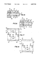
- FIG. 1 is a somewhat schematic fragmentary plan view of the upper face of a portion of the fabrication wafer including a plurality of rectangular LED array chip arrays located in rows and columns, depicting the separation of two adjacent columns of array areas by two spaced parallel scribe grooves in accordance with the present invention
- FIG. 2 is a cross-sectional view along line 2--2 of FIG. 1;
- FIG. 3 corresponds to FIG. 2 and shows a cleaving device positioned in preparation for cleaving the wafer along one of the depicted scribe grooves;
- FIG. 4 corresponds to FIG. 3 and shows the wafer after it has been cleaved
- FIG. 5 is similar to FIG. 3 but shows the wafer reversed to position the other illustrated scribe groove in position for cleaving;
- FIG. 6 illustrates the portion of the chip depicted in FIG. 5 after cleaving
- FIG. 7 is an enlarged fragmentary plan view corresponding generally to FIG. 1 but showing an alternate scribing pattern
- FIG. 8 corresponds to FIG. 7 and shows still another alternate scribing pattern.
- FIG. 1 depicts, somewhat schematically, an enlarged portion of an LED array fabrication wafer 10 on which individual LED array areas 12 are located in rows separated by sawing regions 14 (shown in broken lines) and in columns separated by disposable wafer strips 16 defined by corresponding pairs of spaced scribed cleavage grooves 18 and 20.
- Each of the LED array areas includes, along its longitudinal center line, a row of uniformly spaced light-emitting diode sites 24.
- FIG. 2 is a cross-sectional view showing the two cleavage grooves 18 and 20 at opposite sides of the corresponding disposable strip region 16 and illustrating the location of the individual LED sites 24 at the corresponding ends of the illustrated LED array areas.
- the thickness (A) of a typical wafer of this type could be approximately 350 ( ⁇ m) (micrometers) thick, with the individual diode sites having a center-to-center distance B (FIG. 1) of approximately 65 ⁇ m.
- the width C of the disposable strip 16, defined between cleavage grooves 18 and 20 could be approximately 500 ⁇ m wide and the distance D between each of such grooves and the center of the adjacent diode site is preferably less than, but in no event greater than half the distance B between the centers of adjacent diode sites.
- corresponding channels may be provided in the uppermost layers of wafer material, not shown, as disclosed in detail in my copending U.S. patent application Ser. No. 439,920, filed concurrently herewith and entitled Improving Cleaving of Diode Arrays.
- each LED array chip must be located extremely accurately with respect to the adjacent endmost diode site, it is preferable not to simply provide single straight scribed grooves across the entire wafer, but, rather, as shown in FIG. 1, to scribe individual grooves for each end of each LED array area, originating and terminating in the adjacent sawing streets 14; whereby the required location of each such groove is referenced to fiducial marks on the corresponding array area and minute adjustments of the scribing machine can be performed, as required, for each such groove.
- the wafer is attached to a so-called tape frame, which comprises a thin tensioned sheet of adhesively-faced plastic material 26 to which the lower face of the wafer is adhesively adhered.
- the wafer is then sawed to separate the rows of the array areas, whereupon the tape frame, carrying the separated rows of array areas, is transferred to a cleaving machine.
- FIG. 3 illustrates the portion of the wafer shown in FIG. 2 positioned in a typical cleaving machine that clamps the wafer between an anvil 28 below the array area adjacent groove 18 and a resilient pad 30 on clamp member 32.
- Pressure bar 34 is located above the corresponding disposable strip and is movable downwardly. To cleave the wafer, the pressure bar is driven downwardly, which imparts both a bending force and a sheering force to the wafer, causing it to cleave along a plane defined by groove 18, as shown in FIG. 4. Because the groove 18 is relatively close to the pressure bar, measured along the direction of the rows of array areas, the shearing force, i.e.
- the force tending to move the disposable strip downwardly relative to the adjacent supported area array is relatively large compared to the bending forces imposed on the wafer. Accordingly, the cleavage region of the wafer is subject to asymmetrical forces that cause the ledge 36, if any, to occur on the disposable strip 16 as shown in FIG. 4. Although there is no precise limit on the distance separating the pressure bar from the groove along which the wafer is being cleaved, it is preferable that this distance be less than two or three times the thickness of the wafer.
- the basic principle involved in this technique has previously been employed in the production of glass microtome knives, or the like, as disclosed, for example, in U.S. Pat. Nos. 4,231,503, 4,256,246 and 4,175,684.
- the intent is to establish a curved profile to the fracture to produce a knife-like cutting edge, but the disclosed relationship between the location of the supporting member, the pressure member and the scribed groove is analogous.
- cleaving devices can be employed in accordance with the invention; the important consideration being not the means by which cleaving forces are imparted to the wafer, but the fact that such forces are asymmetrical with respect to the cleavage surface such that any deviation of the resulting cleaved chip surface from a plane normal to the wafer surface tends to be toward the chip and away from the disposable strip.
- the tape frame is reversed 180° in the cleaving machine, as shown in FIG. 5, so that the other groove 20 is now in the same relation to the cleaving machine elements as was groove 18 in the operation depicted in FIGS. 3 and 4. Accordingly, the downward movement of the pressure bar now fractures the wafer material along the plane defined by groove 20, as shown in FIG. 6, whereby ledges 36 and 38, if any, are both on the disposable strip 16.
- the tape frame is removed from the cleaving machine and the separated chips and the disposable strip elements are subsequently removed from the tape frame, with the chips being saved for subsequent use and the disposable strip elements being discarded.
- FIG. 7 corresponds to an enlarged portion of FIG. 1 and depicts an alternate scribing pattern in which two colinear centrally spaced scribing grooves 40a and 40b define corresponding sides of the disposable strip 42 between each confronting pair of LED array areas 44 and
- FIG. 8 similarly depicts another embodiment in which each of the scribing grooves 48a and 48b, at each side of the disposable strip 50, extends only partially across the corresponding end of the adjacent array area 52.
Abstract
Description
Claims (5)
Priority Applications (6)
| Application Number | Priority Date | Filing Date | Title |
|---|---|---|---|
| US07/439,919 US4997792A (en) | 1989-11-21 | 1989-11-21 | Method for separation of diode array chips during fabrication thereof |
| EP91900562A EP0454837B1 (en) | 1989-11-21 | 1990-11-14 | Separation of diode array chips during fabrication thereof |
| PCT/US1990/006489 WO1991008591A1 (en) | 1989-11-21 | 1990-11-14 | Separation of diode array chips during fabrication thereof |
| JP3500814A JPH04503284A (en) | 1989-11-21 | 1990-11-14 | Separation of diode array chip during fabrication of diode array chip |
| DE69029724T DE69029724T2 (en) | 1989-11-21 | 1990-11-14 | SEPARATION OF DIODE MATRIX CHIPS DURING THEIR PRODUCTION |
| US07/662,865 US5300806A (en) | 1989-11-21 | 1991-03-01 | Separation of diode array chips during fabrication thereof |
Applications Claiming Priority (1)
| Application Number | Priority Date | Filing Date | Title |
|---|---|---|---|
| US07/439,919 US4997792A (en) | 1989-11-21 | 1989-11-21 | Method for separation of diode array chips during fabrication thereof |
Related Child Applications (1)
| Application Number | Title | Priority Date | Filing Date |
|---|---|---|---|
| US07/662,865 Division US5300806A (en) | 1989-11-21 | 1991-03-01 | Separation of diode array chips during fabrication thereof |
Publications (1)
| Publication Number | Publication Date |
|---|---|
| US4997792A true US4997792A (en) | 1991-03-05 |
Family
ID=23746686
Family Applications (2)
| Application Number | Title | Priority Date | Filing Date |
|---|---|---|---|
| US07/439,919 Expired - Fee Related US4997792A (en) | 1989-11-21 | 1989-11-21 | Method for separation of diode array chips during fabrication thereof |
| US07/662,865 Expired - Fee Related US5300806A (en) | 1989-11-21 | 1991-03-01 | Separation of diode array chips during fabrication thereof |
Family Applications After (1)
| Application Number | Title | Priority Date | Filing Date |
|---|---|---|---|
| US07/662,865 Expired - Fee Related US5300806A (en) | 1989-11-21 | 1991-03-01 | Separation of diode array chips during fabrication thereof |
Country Status (5)
| Country | Link |
|---|---|
| US (2) | US4997792A (en) |
| EP (1) | EP0454837B1 (en) |
| JP (1) | JPH04503284A (en) |
| DE (1) | DE69029724T2 (en) |
| WO (1) | WO1991008591A1 (en) |
Cited By (10)
| Publication number | Priority date | Publication date | Assignee | Title |
|---|---|---|---|---|
| US5053836A (en) * | 1989-11-21 | 1991-10-01 | Eastman Kodak Company | Cleaving of diode arrays with scribing channels |
| US5393706A (en) * | 1993-01-07 | 1995-02-28 | Texas Instruments Incorporated | Integrated partial sawing process |
| US5454002A (en) * | 1994-04-28 | 1995-09-26 | The Board Of Regents Of The University Of Oklahoma | High temperature semiconductor diode laser |
| US5650348A (en) * | 1995-06-07 | 1997-07-22 | Lsi Logic Corporation | Method of making an integrated circuit chip having an array of logic gates |
| US20030039901A1 (en) * | 2000-08-31 | 2003-02-27 | Micron Technology, Inc. | Precision fiducial |
| US20040171184A1 (en) * | 2001-04-27 | 2004-09-02 | Semiconductor Energy Laboratory Co., Ltd. | Display device and manufacturing method thereof |
| US20080116240A1 (en) * | 2003-12-22 | 2008-05-22 | Edwards Mark S | Method and apparatus for fracturing seal rings |
| CN104617014A (en) * | 2014-12-22 | 2015-05-13 | 苏州固锝电子股份有限公司 | Efficient processing device for diode device |
| CN104617022A (en) * | 2014-12-22 | 2015-05-13 | 苏州固锝电子股份有限公司 | Turnover device applied to manufacture of axial type diode |
| CN104871378A (en) * | 2012-12-18 | 2015-08-26 | 奥斯兰姆奥普托半导体有限责任公司 | Method for producing semi-conductor laser elements and semi-conductor laser element |
Families Citing this family (3)
| Publication number | Priority date | Publication date | Assignee | Title |
|---|---|---|---|---|
| US5872386A (en) * | 1995-07-17 | 1999-02-16 | Sii R&D Center Inc. | Wafer layout of semiconductor device |
| US20060261118A1 (en) * | 2005-05-17 | 2006-11-23 | Cox Judy K | Method and apparatus for separating a pane of brittle material from a moving ribbon of the material |
| JP5141076B2 (en) * | 2006-06-05 | 2013-02-13 | 株式会社デンソー | Semiconductor device |
Citations (15)
| Publication number | Priority date | Publication date | Assignee | Title |
|---|---|---|---|---|
| US4068788A (en) * | 1975-09-29 | 1978-01-17 | Rca Corporation | Method for cracking brittle material |
| US4175684A (en) * | 1978-07-31 | 1979-11-27 | Butler James K | Mechanical glass knife scorer/breaker |
| US4231503A (en) * | 1979-03-05 | 1980-11-04 | Butler James K | Microtomy knife breaker |
| US4256246A (en) * | 1978-07-04 | 1981-03-17 | Lkb-Produkter Ab | Device for breaking a glass plate so as to obtain a sharp edge |
| US4355457A (en) * | 1980-10-29 | 1982-10-26 | Rca Corporation | Method of forming a mesa in a semiconductor device with subsequent separation into individual devices |
| JPS60216565A (en) * | 1985-03-11 | 1985-10-30 | Hitachi Ltd | Dicing method for wafer |
| US4604161A (en) * | 1985-05-02 | 1986-08-05 | Xerox Corporation | Method of fabricating image sensor arrays |
| US4605944A (en) * | 1984-09-11 | 1986-08-12 | Sanyo Electric Co., Ltd. | LED array device for printer |
| US4610079A (en) * | 1980-01-22 | 1986-09-09 | Tokyo Shibaura Denki Kabushiki Kaisha | Method of dicing a semiconductor wafer |
| US4668333A (en) * | 1985-12-13 | 1987-05-26 | Xerox Corporation | Image sensor array for assembly with like arrays to form a longer array |
| JPS6392026A (en) * | 1986-10-06 | 1988-04-22 | Mitsubishi Electric Corp | Semiconductor device |
| US4814296A (en) * | 1987-08-28 | 1989-03-21 | Xerox Corporation | Method of fabricating image sensor dies for use in assembling arrays |
| US4822755A (en) * | 1988-04-25 | 1989-04-18 | Xerox Corporation | Method of fabricating large area semiconductor arrays |
| US4900283A (en) * | 1984-11-26 | 1990-02-13 | Kentek Information Systems, Inc. | Method for arranging chips each having an array of semiconductor light emitting elements |
| US4904617A (en) * | 1987-09-17 | 1990-02-27 | Siemens Aktiengesellschaft | Method for separating monolithically produced laser diodes |
Family Cites Families (11)
| Publication number | Priority date | Publication date | Assignee | Title |
|---|---|---|---|---|
| DE1652512B2 (en) * | 1967-05-29 | 1976-08-26 | Siemens AG, 1000 Berlin und 8000 München | METHOD FOR MANUFACTURING SEMICONDUCTOR COMPONENTS |
| US3883887A (en) * | 1973-02-09 | 1975-05-13 | Astronics Corp | Metal oxide switching elements |
| US4011575A (en) * | 1974-07-26 | 1977-03-08 | Litton Systems, Inc. | Light emitting diode array having a plurality of conductive paths for each light emitting diode |
| JPS54102886A (en) * | 1978-01-31 | 1979-08-13 | Futaba Denshi Kogyo Kk | Light emitting diode indicator |
| DE3172935D1 (en) * | 1980-02-28 | 1986-01-02 | Toshiba Kk | Iii - v group compound semiconductor light-emitting element and method of producing the same |
| DD200295A1 (en) * | 1981-08-12 | 1983-04-06 | Guenter Claus | LED DISPLAY WITH HIGH INFORMATION CONTENT |
| JPS6020590A (en) * | 1983-07-14 | 1985-02-01 | Sanyo Electric Co Ltd | Method for cutting light emitting diode |
| DE3328902A1 (en) * | 1983-08-10 | 1985-02-28 | Siemens AG, 1000 Berlin und 8000 München | DISPLAY WITH A NUMBER OF LIGHT-EMITTING SEMICONDUCTOR COMPONENTS |
| JPS60144985A (en) * | 1983-12-30 | 1985-07-31 | Fujitsu Ltd | Manufacture of semiconductor light-emitting element |
| JPS6164176A (en) * | 1984-09-05 | 1986-04-02 | Sanyo Electric Co Ltd | Dividing method of light-emitting diode |
| US4868616A (en) * | 1986-12-11 | 1989-09-19 | Energy Conversion Devices, Inc. | Amorphous electronic matrix array for liquid crystal display |
-
1989
- 1989-11-21 US US07/439,919 patent/US4997792A/en not_active Expired - Fee Related
-
1990
- 1990-11-14 JP JP3500814A patent/JPH04503284A/en active Pending
- 1990-11-14 DE DE69029724T patent/DE69029724T2/en not_active Expired - Fee Related
- 1990-11-14 WO PCT/US1990/006489 patent/WO1991008591A1/en active IP Right Grant
- 1990-11-14 EP EP91900562A patent/EP0454837B1/en not_active Expired - Lifetime
-
1991
- 1991-03-01 US US07/662,865 patent/US5300806A/en not_active Expired - Fee Related
Patent Citations (15)
| Publication number | Priority date | Publication date | Assignee | Title |
|---|---|---|---|---|
| US4068788A (en) * | 1975-09-29 | 1978-01-17 | Rca Corporation | Method for cracking brittle material |
| US4256246A (en) * | 1978-07-04 | 1981-03-17 | Lkb-Produkter Ab | Device for breaking a glass plate so as to obtain a sharp edge |
| US4175684A (en) * | 1978-07-31 | 1979-11-27 | Butler James K | Mechanical glass knife scorer/breaker |
| US4231503A (en) * | 1979-03-05 | 1980-11-04 | Butler James K | Microtomy knife breaker |
| US4610079A (en) * | 1980-01-22 | 1986-09-09 | Tokyo Shibaura Denki Kabushiki Kaisha | Method of dicing a semiconductor wafer |
| US4355457A (en) * | 1980-10-29 | 1982-10-26 | Rca Corporation | Method of forming a mesa in a semiconductor device with subsequent separation into individual devices |
| US4605944A (en) * | 1984-09-11 | 1986-08-12 | Sanyo Electric Co., Ltd. | LED array device for printer |
| US4900283A (en) * | 1984-11-26 | 1990-02-13 | Kentek Information Systems, Inc. | Method for arranging chips each having an array of semiconductor light emitting elements |
| JPS60216565A (en) * | 1985-03-11 | 1985-10-30 | Hitachi Ltd | Dicing method for wafer |
| US4604161A (en) * | 1985-05-02 | 1986-08-05 | Xerox Corporation | Method of fabricating image sensor arrays |
| US4668333A (en) * | 1985-12-13 | 1987-05-26 | Xerox Corporation | Image sensor array for assembly with like arrays to form a longer array |
| JPS6392026A (en) * | 1986-10-06 | 1988-04-22 | Mitsubishi Electric Corp | Semiconductor device |
| US4814296A (en) * | 1987-08-28 | 1989-03-21 | Xerox Corporation | Method of fabricating image sensor dies for use in assembling arrays |
| US4904617A (en) * | 1987-09-17 | 1990-02-27 | Siemens Aktiengesellschaft | Method for separating monolithically produced laser diodes |
| US4822755A (en) * | 1988-04-25 | 1989-04-18 | Xerox Corporation | Method of fabricating large area semiconductor arrays |
Cited By (23)
| Publication number | Priority date | Publication date | Assignee | Title |
|---|---|---|---|---|
| US5053836A (en) * | 1989-11-21 | 1991-10-01 | Eastman Kodak Company | Cleaving of diode arrays with scribing channels |
| US5393706A (en) * | 1993-01-07 | 1995-02-28 | Texas Instruments Incorporated | Integrated partial sawing process |
| US5454002A (en) * | 1994-04-28 | 1995-09-26 | The Board Of Regents Of The University Of Oklahoma | High temperature semiconductor diode laser |
| WO1995030261A1 (en) * | 1994-04-28 | 1995-11-09 | The Board Of Regents Of The University Of Oklahoma | High temperature semiconductor diode laser |
| US5629097A (en) * | 1994-04-28 | 1997-05-13 | The Board Of Regents Of The University Of Oklahoma | Apparatus for fabricating semiconductor lasers |
| US5776794A (en) * | 1994-04-28 | 1998-07-07 | The Board Of Regents Of The University Of Oklahoma | Method for fabricating semiconductor laser |
| US5650348A (en) * | 1995-06-07 | 1997-07-22 | Lsi Logic Corporation | Method of making an integrated circuit chip having an array of logic gates |
| US6820525B2 (en) * | 2000-08-31 | 2004-11-23 | Micron Technology, Inc. | Precision Fiducial |
| US20030039901A1 (en) * | 2000-08-31 | 2003-02-27 | Micron Technology, Inc. | Precision fiducial |
| US6855961B2 (en) * | 2001-04-27 | 2005-02-15 | Semiconductor Energy Laboratory Co., Ltd. | Display device and manufacturing method thereof |
| US20040171184A1 (en) * | 2001-04-27 | 2004-09-02 | Semiconductor Energy Laboratory Co., Ltd. | Display device and manufacturing method thereof |
| US20060065960A1 (en) * | 2001-04-27 | 2006-03-30 | Semiconductor Energy Laboratory Co., Ltd. | Display device and manufacturing method thereof |
| US7067395B2 (en) | 2001-04-27 | 2006-06-27 | Semiconductor Energy Laboratory Co., Ltd. | Display device and manufacturing method thereof |
| US7535018B2 (en) | 2001-04-27 | 2009-05-19 | Semiconductor Energy Laboratory Co., Ltd. | Display device and manufacturing method thereof |
| US20080116240A1 (en) * | 2003-12-22 | 2008-05-22 | Edwards Mark S | Method and apparatus for fracturing seal rings |
| CN104871378B (en) * | 2012-12-18 | 2017-07-21 | 奥斯兰姆奥普托半导体有限责任公司 | Method and semiconductor laser component for manufacturing semiconductor laser component |
| CN104871378A (en) * | 2012-12-18 | 2015-08-26 | 奥斯兰姆奥普托半导体有限责任公司 | Method for producing semi-conductor laser elements and semi-conductor laser element |
| US9608401B2 (en) | 2012-12-18 | 2017-03-28 | Osram Opto Semiconductors Gmbh | Method for producing semiconductor laser elements and semi-conductor laser element |
| CN104617022A (en) * | 2014-12-22 | 2015-05-13 | 苏州固锝电子股份有限公司 | Turnover device applied to manufacture of axial type diode |
| CN104617014A (en) * | 2014-12-22 | 2015-05-13 | 苏州固锝电子股份有限公司 | Efficient processing device for diode device |
| CN104617022B (en) * | 2014-12-22 | 2017-09-26 | 苏州固锝电子股份有限公司 | The turnover device manufactured for axialmode diode |
| CN107978547A (en) * | 2014-12-22 | 2018-05-01 | 苏州固锝电子股份有限公司 | Diode component production epicyclical mechanism |
| CN104617014B (en) * | 2014-12-22 | 2018-09-07 | 苏州固锝电子股份有限公司 | Highly-efficient processing device for diode component |
Also Published As
| Publication number | Publication date |
|---|---|
| EP0454837B1 (en) | 1997-01-15 |
| JPH04503284A (en) | 1992-06-11 |
| US5300806A (en) | 1994-04-05 |
| WO1991008591A1 (en) | 1991-06-13 |
| DE69029724D1 (en) | 1997-02-27 |
| DE69029724T2 (en) | 1997-07-31 |
| EP0454837A1 (en) | 1991-11-06 |
Similar Documents
| Publication | Publication Date | Title |
|---|---|---|
| US4997792A (en) | Method for separation of diode array chips during fabrication thereof | |
| JP2597447B2 (en) | Method for manufacturing semiconductor device | |
| JP5216040B2 (en) | Method for dividing brittle material substrate | |
| JP5187421B2 (en) | Breaking method for brittle material substrate | |
| US20100015781A1 (en) | Semiconductor substrate, and semiconductor device and method of manufacturing the semiconductor device | |
| JP5210409B2 (en) | Break device | |
| TW201144244A (en) | Cutter wheel, scribing method and cutting method for fragile material substrate using the cutter wheel, and method of manufacturing cutter wheel | |
| TWI623402B (en) | Method and device for cutting brittle material substrate | |
| JP5228852B2 (en) | Substrate dividing method and substrate dividing apparatus | |
| KR102259441B1 (en) | Breaking apparatus and dividing method | |
| TW201315557A (en) | Mother substrate splitting method | |
| JP2010253612A (en) | Workpiece cutting device and method | |
| CN111916356A (en) | Breaking method of metal laminated ceramic substrate | |
| CN104552628A (en) | Expander, breaking apparatus and dividing method | |
| US4997793A (en) | Method of improving cleaving of diode arrays | |
| TWI548478B (en) | Verfahren zum trennen einer runden planplatte aus sproedbruechigem material in mehrere rechteckige einzelplatten mittels laser | |
| KR20150044374A (en) | Spring supportplate, fracture device and dividing method | |
| JP3834099B2 (en) | LCD glass plate cutting device | |
| KR20050082449A (en) | Cell cutting method for plastic film lcd and apparatus thereof | |
| JPS60144985A (en) | Manufacture of semiconductor light-emitting element | |
| TWI698329B (en) | Splitting method and device for laminated substrate | |
| JP2005109061A (en) | Jig for manufacturing semiconductor device, manufacturing method for jig, and manufacturing method for semiconductor device | |
| KR100670600B1 (en) | Scribing apparatus | |
| JPH11274653A (en) | Method for cleaving semiconductor laser substrate | |
| JP2003261345A (en) | Method for cracking rigid brittle plate |
Legal Events
| Date | Code | Title | Description |
|---|---|---|---|
| AS | Assignment |
Owner name: EASTMAN KODAK COMPANY, NEW YORK Free format text: ASSIGNMENT OF ASSIGNORS INTEREST.;ASSIGNOR:MC CLURG, SCOTT D.;REEL/FRAME:005230/0024 Effective date: 19891115 |
|
| FEPP | Fee payment procedure |
Free format text: PAYOR NUMBER ASSIGNED (ORIGINAL EVENT CODE: ASPN); ENTITY STATUS OF PATENT OWNER: LARGE ENTITY |
|
| FPAY | Fee payment |
Year of fee payment: 4 |
|
| FEPP | Fee payment procedure |
Free format text: PAYER NUMBER DE-ASSIGNED (ORIGINAL EVENT CODE: RMPN); ENTITY STATUS OF PATENT OWNER: LARGE ENTITY Free format text: PAYOR NUMBER ASSIGNED (ORIGINAL EVENT CODE: ASPN); ENTITY STATUS OF PATENT OWNER: LARGE ENTITY |
|
| REMI | Maintenance fee reminder mailed | ||
| LAPS | Lapse for failure to pay maintenance fees | ||
| FP | Lapsed due to failure to pay maintenance fee |
Effective date: 19990305 |
|
| STCH | Information on status: patent discontinuation |
Free format text: PATENT EXPIRED DUE TO NONPAYMENT OF MAINTENANCE FEES UNDER 37 CFR 1.362 |