US4988643A - Self-aligning metal interconnect fabrication - Google Patents
Self-aligning metal interconnect fabrication Download PDFInfo
- Publication number
- US4988643A US4988643A US07/419,284 US41928489A US4988643A US 4988643 A US4988643 A US 4988643A US 41928489 A US41928489 A US 41928489A US 4988643 A US4988643 A US 4988643A
- Authority
- US
- United States
- Prior art keywords
- over
- oxide
- source
- interconnect
- conductor
- Prior art date
- Legal status (The legal status is an assumption and is not a legal conclusion. Google has not performed a legal analysis and makes no representation as to the accuracy of the status listed.)
- Expired - Lifetime
Links
Images

Classifications
-
- H—ELECTRICITY
- H01—ELECTRIC ELEMENTS
- H01L—SEMICONDUCTOR DEVICES NOT COVERED BY CLASS H10
- H01L21/00—Processes or apparatus adapted for the manufacture or treatment of semiconductor or solid state devices or of parts thereof
- H01L21/02—Manufacture or treatment of semiconductor devices or of parts thereof
- H01L21/04—Manufacture or treatment of semiconductor devices or of parts thereof the devices having at least one potential-jump barrier or surface barrier, e.g. PN junction, depletion layer or carrier concentration layer
- H01L21/18—Manufacture or treatment of semiconductor devices or of parts thereof the devices having at least one potential-jump barrier or surface barrier, e.g. PN junction, depletion layer or carrier concentration layer the devices having semiconductor bodies comprising elements of Group IV of the Periodic System or AIIIBV compounds with or without impurities, e.g. doping materials
- H01L21/30—Treatment of semiconductor bodies using processes or apparatus not provided for in groups H01L21/20 - H01L21/26
- H01L21/31—Treatment of semiconductor bodies using processes or apparatus not provided for in groups H01L21/20 - H01L21/26 to form insulating layers thereon, e.g. for masking or by using photolithographic techniques; After treatment of these layers; Selection of materials for these layers
- H01L21/314—Inorganic layers
- H01L21/316—Inorganic layers composed of oxides or glassy oxides or oxide based glass
- H01L21/3165—Inorganic layers composed of oxides or glassy oxides or oxide based glass formed by oxidation
- H01L21/31683—Inorganic layers composed of oxides or glassy oxides or oxide based glass formed by oxidation of metallic layers, e.g. Al deposited on the body, e.g. formation of multi-layer insulating structures
-
- H—ELECTRICITY
- H01—ELECTRIC ELEMENTS
- H01L—SEMICONDUCTOR DEVICES NOT COVERED BY CLASS H10
- H01L21/00—Processes or apparatus adapted for the manufacture or treatment of semiconductor or solid state devices or of parts thereof
- H01L21/02—Manufacture or treatment of semiconductor devices or of parts thereof
- H01L21/04—Manufacture or treatment of semiconductor devices or of parts thereof the devices having at least one potential-jump barrier or surface barrier, e.g. PN junction, depletion layer or carrier concentration layer
- H01L21/18—Manufacture or treatment of semiconductor devices or of parts thereof the devices having at least one potential-jump barrier or surface barrier, e.g. PN junction, depletion layer or carrier concentration layer the devices having semiconductor bodies comprising elements of Group IV of the Periodic System or AIIIBV compounds with or without impurities, e.g. doping materials
- H01L21/28—Manufacture of electrodes on semiconductor bodies using processes or apparatus not provided for in groups H01L21/20 - H01L21/268
- H01L21/283—Deposition of conductive or insulating materials for electrodes conducting electric current
- H01L21/285—Deposition of conductive or insulating materials for electrodes conducting electric current from a gas or vapour, e.g. condensation
- H01L21/28506—Deposition of conductive or insulating materials for electrodes conducting electric current from a gas or vapour, e.g. condensation of conductive layers
- H01L21/28512—Deposition of conductive or insulating materials for electrodes conducting electric current from a gas or vapour, e.g. condensation of conductive layers on semiconductor bodies comprising elements of Group IV of the Periodic System
- H01L21/28525—Deposition of conductive or insulating materials for electrodes conducting electric current from a gas or vapour, e.g. condensation of conductive layers on semiconductor bodies comprising elements of Group IV of the Periodic System the conductive layers comprising semiconducting material
-
- H—ELECTRICITY
- H01—ELECTRIC ELEMENTS
- H01L—SEMICONDUCTOR DEVICES NOT COVERED BY CLASS H10
- H01L21/00—Processes or apparatus adapted for the manufacture or treatment of semiconductor or solid state devices or of parts thereof
- H01L21/70—Manufacture or treatment of devices consisting of a plurality of solid state components formed in or on a common substrate or of parts thereof; Manufacture of integrated circuit devices or of parts thereof
- H01L21/71—Manufacture of specific parts of devices defined in group H01L21/70
- H01L21/768—Applying interconnections to be used for carrying current between separate components within a device comprising conductors and dielectrics
- H01L21/76838—Applying interconnections to be used for carrying current between separate components within a device comprising conductors and dielectrics characterised by the formation and the after-treatment of the conductors
- H01L21/76886—Modifying permanently or temporarily the pattern or the conductivity of conductive members, e.g. formation of alloys, reduction of contact resistances
- H01L21/76889—Modifying permanently or temporarily the pattern or the conductivity of conductive members, e.g. formation of alloys, reduction of contact resistances by forming silicides of refractory metals
-
- H—ELECTRICITY
- H01—ELECTRIC ELEMENTS
- H01L—SEMICONDUCTOR DEVICES NOT COVERED BY CLASS H10
- H01L21/00—Processes or apparatus adapted for the manufacture or treatment of semiconductor or solid state devices or of parts thereof
- H01L21/02—Manufacture or treatment of semiconductor devices or of parts thereof
- H01L21/02104—Forming layers
- H01L21/02107—Forming insulating materials on a substrate
- H01L21/02109—Forming insulating materials on a substrate characterised by the type of layer, e.g. type of material, porous/non-porous, pre-cursors, mixtures or laminates
- H01L21/02112—Forming insulating materials on a substrate characterised by the type of layer, e.g. type of material, porous/non-porous, pre-cursors, mixtures or laminates characterised by the material of the layer
- H01L21/02123—Forming insulating materials on a substrate characterised by the type of layer, e.g. type of material, porous/non-porous, pre-cursors, mixtures or laminates characterised by the material of the layer the material containing silicon
- H01L21/02164—Forming insulating materials on a substrate characterised by the type of layer, e.g. type of material, porous/non-porous, pre-cursors, mixtures or laminates characterised by the material of the layer the material containing silicon the material being a silicon oxide, e.g. SiO2
-
- H—ELECTRICITY
- H01—ELECTRIC ELEMENTS
- H01L—SEMICONDUCTOR DEVICES NOT COVERED BY CLASS H10
- H01L21/00—Processes or apparatus adapted for the manufacture or treatment of semiconductor or solid state devices or of parts thereof
- H01L21/02—Manufacture or treatment of semiconductor devices or of parts thereof
- H01L21/02104—Forming layers
- H01L21/02107—Forming insulating materials on a substrate
- H01L21/02109—Forming insulating materials on a substrate characterised by the type of layer, e.g. type of material, porous/non-porous, pre-cursors, mixtures or laminates
- H01L21/02112—Forming insulating materials on a substrate characterised by the type of layer, e.g. type of material, porous/non-porous, pre-cursors, mixtures or laminates characterised by the material of the layer
- H01L21/02123—Forming insulating materials on a substrate characterised by the type of layer, e.g. type of material, porous/non-porous, pre-cursors, mixtures or laminates characterised by the material of the layer the material containing silicon
- H01L21/0217—Forming insulating materials on a substrate characterised by the type of layer, e.g. type of material, porous/non-porous, pre-cursors, mixtures or laminates characterised by the material of the layer the material containing silicon the material being a silicon nitride not containing oxygen, e.g. SixNy or SixByNz
-
- H—ELECTRICITY
- H01—ELECTRIC ELEMENTS
- H01L—SEMICONDUCTOR DEVICES NOT COVERED BY CLASS H10
- H01L21/00—Processes or apparatus adapted for the manufacture or treatment of semiconductor or solid state devices or of parts thereof
- H01L21/02—Manufacture or treatment of semiconductor devices or of parts thereof
- H01L21/02104—Forming layers
- H01L21/02107—Forming insulating materials on a substrate
- H01L21/02225—Forming insulating materials on a substrate characterised by the process for the formation of the insulating layer
- H01L21/02227—Forming insulating materials on a substrate characterised by the process for the formation of the insulating layer formation by a process other than a deposition process
- H01L21/0223—Forming insulating materials on a substrate characterised by the process for the formation of the insulating layer formation by a process other than a deposition process formation by oxidation, e.g. oxidation of the substrate
- H01L21/02233—Forming insulating materials on a substrate characterised by the process for the formation of the insulating layer formation by a process other than a deposition process formation by oxidation, e.g. oxidation of the substrate of the semiconductor substrate or a semiconductor layer
- H01L21/02236—Forming insulating materials on a substrate characterised by the process for the formation of the insulating layer formation by a process other than a deposition process formation by oxidation, e.g. oxidation of the substrate of the semiconductor substrate or a semiconductor layer group IV semiconductor
- H01L21/02238—Forming insulating materials on a substrate characterised by the process for the formation of the insulating layer formation by a process other than a deposition process formation by oxidation, e.g. oxidation of the substrate of the semiconductor substrate or a semiconductor layer group IV semiconductor silicon in uncombined form, i.e. pure silicon
-
- H—ELECTRICITY
- H01—ELECTRIC ELEMENTS
- H01L—SEMICONDUCTOR DEVICES NOT COVERED BY CLASS H10
- H01L21/00—Processes or apparatus adapted for the manufacture or treatment of semiconductor or solid state devices or of parts thereof
- H01L21/02—Manufacture or treatment of semiconductor devices or of parts thereof
- H01L21/02104—Forming layers
- H01L21/02107—Forming insulating materials on a substrate
- H01L21/02225—Forming insulating materials on a substrate characterised by the process for the formation of the insulating layer
- H01L21/02227—Forming insulating materials on a substrate characterised by the process for the formation of the insulating layer formation by a process other than a deposition process
- H01L21/02255—Forming insulating materials on a substrate characterised by the process for the formation of the insulating layer formation by a process other than a deposition process formation by thermal treatment
Definitions
- the present invention relates to semiconductor processing and, more particularly, to a method of forming semiconductor devices and interconnects therebetween.
- a major objective of the present invention is to provide for interconnects without vias and with minimum spacing and overlap design rules.
- MOS transistor includes a source, a drain and a gate which can be used to control a current between the source and drain. Connecting such a transistor to other circuit devices on an integrated circuit requires that conductors be electrically connected to its source, drain and gate.
- the gate includes a metal or doped polysilicon (polycrystalline silicon) pedestal. The source and drain are formed in a silicon substrate to either side of this pedestal.
- an insulating oxide is deposited over the source, drain and gate pedestal. Vias are formed through the oxide layer, for example, over the source and drain.
- a metal layer is deposited and patterned over the oxide. The metal layer accesses the source and drain through the vias to define conductive leads for the source and drain.
- a "silicidable metal” is a metal that can be sintered with an adjacent silicon material to form a metal silicide.
- a silicidable metal is deposited over the transistor without an intermediate insulating layer. Sintering causes the formation of silicide over the source and drain regions, as well as over the gate pedestal. A wet etch is used to remove the metal over regions where silicide has not formed.
- the self-aligning approach can be extended to provide local interconnects by selectively reacting portions of the metal layer.
- the reacting can be done with nitrogen as disclosed by Thomas Tang, Che-Chia Wei, Roger Haken, Thomas Holloway, Chang-Feng Wan and Monte Douglas in "VLSI Local Interconnect Level Using Titanium Nitride", IEDM, 1985.
- silicide can be formed over the metal layer as disclosed by Devereaux C. Chen, Simon S. Wong, Paul Vande Voorde, P. Merchant, Tom R. Cass, Jun Amano, and Kuang-Yi Chiu in "A New Device Interconnect Scheme for Sub-Micron VLSI", IEDM, 1984.
- the reacting material is patterned over the metal using a mask. Therefore, strict masking tolerances are still required to ensure that interconnect metal does not short to the gate silicide.
- a more serious disadvantage of the self-aligning approaches is that bridging interconnects are not provided conveniently.
- a bridging interconnect is one which crosses another interconnect without making an electrical connection thereto.
- Bridging interconnects are easily defined in conventional MOS processing in which the intermediate dielectric layer provides the required electrical insulation except where vias are formed.
- the self-aligning approaches do not form an dielectric layer through which vias are to be formed. While this provides for more compact devices, it makes insulated conductor crossings more difficult to obtain. In fact, the art cited above does not suggest how bridging interconnects can be made.
- an oxide layer is grown over a gate pedestal, or similar structure, and an "underlying" interconnect to isolate them from an "overlaying" interconnect.
- an oxide retarding layer e.g., silicon nitride
- Silicide formations can be defined over source and drain regions and over the exposed underlying interconnect.
- the overlaying interconnect can be defined to extend from a source or drain region to the silicided underlying interconnect.
- the overlaying interconnect can cross over the oxide coated underlying interconnect so as to remain electrically insulated therefrom. Thus, a bridging interconnect is provided.
- oxide left over the gate pedestal insulates it from the overlaying interconnect relaxing masking tolerances for the overlaying interconnects.
- a remote interconnect is an interconnect that provides for electrical connections between transistors, but requires a local interconnect to a transistor of interest.
- the transistor includes a gate, a source and a drain. Since, source and drain are treated similarly in the context of this application, they are referred to collectively as current-carrying regions herein.
- the present invention provides for the formation of a local overlaying interconnect between a first current-carrying region and an underlying first remote interconnect.
- the local interconnect is electrically connected to the first-current-carrying region through an intermediate silicide formation and is electrically connected to the first remote interconnect through another intermediate silicide formation.
- the local interconnect is electrically insulated from a second underlying remote interconnect by an oxide formation. Furthermore, an oxide formation over the gate prevents shorting of the local interconnect thereto.
- the present invention provides that gates and some interconnects are covered with oxide during silicide formation.
- oxide sidewalls provided insulation to the sides of the gates, but the anisotropic etch used to defined the sidewalls removed all oxide from the top of the gate and remote interconnect structures.
- silicide was formed over the exposed gate and interconnect structures.
- the silicide over the interconnects made it difficult to define bridging interconnects.
- the silicide over the gate required design tolerances to avoiding shorting by local interconnects.
- the gates are covered with oxide, rather than silicide, so tolerances required to prevent shorting of a local interconnect to a gate can be relaxed considerably.
- bridging (overlaying) interconnects can be made to silicide-coated remote interconnects over oxide-coated remote interconnects.
- an additional masking step is required to define the nitride formation which prevents oxide formation over some remote interconnects, this masking step is subject to relaxed tolerances.
- the nitride over a first remote interconnect should not extend to current-carrying regions and remote interconnects, unless electrical connection is intended. However, this allows nitride mask alignment tolerances on the order of a feature size. It is not necessary for the nitride mask to cover the remote interconnect completely, since, in general, a partial physical contact between the silicide and local interconnect to be formed will suffice for an electrical connection.
- the present invention provides for bridging interconnects in the context of a self-aligning silicide process and the advantages in device density and masking tolerances provided by such processes over non-self-aligning processes. Furthermore, the present silicide self-aligning process provides further relaxation of masking tolerances to provide for smaller transistors and other integrated circuit devices.
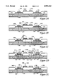
- FIG. 1A is a plan view and FIG. 1B is a sectional view of a semiconductor structure in accordance with the present invention.
- FIG. 1A is shown with cutaways to disclose polysilicon below oxide insulation and source and drain regions below silicide.
- FIGS. 2A-2E are sectional views of the semiconductor structure of FIGS. 1A and 1B at successive stages in its fabrication in accordance with the method of the present invention.
- a CMOS inverter 100 comprises an NMOS transistor 102, a first remote interconnect 104, a second remote interconnect 106, and a PMOS transistor 108, as shown in FIGS. 1A and 1B. These structures are fabricated on a substrate 110 of p-type silicon which includes an n-type region, n-well 112 at which PMOS transistor 108 is fabricated, as shown in FIG. 1B. Transistors 102 and 108 are isolated from each other and neighboring transistors (not shown) by "left", “center” and “right” field oxides 114, 116, and 118, respectively.
- NMOS transistor 102 comprises a source 120 and a drain 122, between which current can be carried at a rate regulated by the voltage at the gate 124 of transistor 102.
- PMOS transistor 108 comprises a drain 126, a source 128, and a gate 130.
- CMOS inverter 100 is implemented using a local interconnect 132 between NMOS drain 122 and PMOS drain 126.
- Local interconnect 132 makes electrical contact with NMOS drain 122 through a silicide formation 134 and with PMOS drain 126 through a silicide formation 136.
- local interconnect 132 makes electrical contact with remote interconnect 104 via a silicide formation 138.
- Local interconnect 132 extends over remote interconnect 106 and is electrically insulated therefrom by an oxide formation 140. Thus, a bridging local interconnect is achieved.
- Oxide formations 142 and 144 over gates 124 and 130 prevent shorting thereto by local interconnect 132 despite any moderate masking misalignment relative to gates 124 and 130. As indicated below, the oxide over the gates thus minimizes masking tolerances during the formation of local interconnect 132. Devices fabricated in accordance with the described prior art self-aligning silicide processes would have silicide rather than oxide on top of their gates and would not provide a bridging interconnect. Furthermore, a tolerance is required to prevent interconnect material from shorting to the gate preventing the transistor from being as compact as desired.
- NMOS source 120 Electrical access to NMOS source 120 is provided by a local interconnect 146 which contacts a silicide formation 148 over source 120 and extends over field oxide 114. Likewise, a local interconnect 150 contacts a silicide formation 152 over PMOS source 128 and extends over field oxide 118.
- CMOS inverter 100 can be fabricated in a convention manner until the structure of FIG. 2A is achieved.
- N-well 112 is defined by introducing dopant in the region of p-type substrate 110 at which PMOS transistor 108 is to be defined so that the conductivity type of the region is reversed.
- Field oxides 114, 116, and 118 are formed conventionally.
- a relatively short oxide growth cycle is then used to define gate oxides 202 between the field oxides.
- Polysilicon is then deposited and heavily doped over the field and gate oxides to increase its conductivity.
- the polysilicon is then lithographically patterned to define gates 124 and 130 and remote interconnects 104 and 106.
- the present invention departs from conventional processing by depositing a nitride layer over the structure of FIG. 2A.
- a nitride cap 204 is photolithographically defined from this layer, resulting in the structure of FIG. 2B.
- the purpose of nitride cap 204 is to prevent or limit oxide growth over remote interconnect 104 so that an electrical connection can be made thereto by local interconnect 132, as indicated by comparison of FIGS. 1B and 2B.
- nitride cap 204 involves a masking step not required in the prior art, and thus introduces an extra tolerance which must be considered. This tolerance is very relaxed.
- the nitride can extend to the left over the left edge of field oxide 116 and even over gate oxide 202 over region 206 where drain 122 is to be defined.
- the left limit is gate 124, which must not be contacted by the nitride or else interconnect 104 and drain 122 could short to it once local interconnect 132 is formed.
- Nitride cap 204 can extend to the right of remote interconnect 104 short of contacting remote interconnect 106. It is not necessary that remote interconnect 104 be entirely covered. It is sufficient that nitride cap 204 cover an area large enough for forming an electrical contact.
- the tolerances involved in forming nitride cap 204 are on the order of the feature size for inverter 100.
- Oxide is grown over the structure of FIG. 2B.
- the oxide grows relatively rapidly over the gates 124 and 130 and remote interconnect 106, and relatively slowly over the diffused source and drain regions 206, 208, 210 and 212, FIG. 2B.
- source and drain regions 206, 208, 210 and 212 can be lightly doped prior to this oxidation.
- Polysilicon is polycrystalline so that its surface is inherently less smooth than the surface of the single crystal substrate at source and drain regions 206, 208, 210 and 212. Moreover, the previous heavy doping of the polysilicon further enhances the growth rate. Crystalline substrate 110 is not heavily doped at this point so the growth rate thereover is very slow compared to that over the heavily doped polysilicon. This differential oxide growth is enhanced by low temperature oxidation, e.g., at about 800° C. At most negligible oxide growth occurs over remote interconnect 104 where it is protected by nitride cap 204.
- the oxide is then etched until it is removed over source and drain regions 206, 208, 210 and 212.
- the originally thick oxide over gates 124 and 130 is only partially removed during this etch establishing oxide formations 140, 142, and 144 over remote interconnect 106 and gates 124 and 130, as shown in FIG. 2D.
- the etch is anisotropic so that sidewalls 214 on these structures retain most of their lateral thickness.
- Nitride cap 204 is removed using a wet etch.
- An n-type dopant is implanted in regions 206 and 208 to define NMOS source 120 and NMOS drain 122, and a p-type dopant is implanted in the regions 210 and 212 to define PMOS drain 126 and PMOS source 128.
- the resulting structure is shown in FIG. 2D.
- Titanium is deposited over the structure of FIG. 2D and sintered to form silicide wherever silicon is exposed, but not where silicon dioxide is exposed.
- Other silicidable metals preferably refractory metals, can be used as alternatives to titanium.
- the metal which has not converted to silicide is then etched away, yielding the structure of FIG. 2E.
- silicide formation 148 at source 120, silicide formation 134 at drain 122, silicide formation 138 over remote interconnect 104, silicide formation 136 at drain 126, and silicide formation 152 at source 128 are created. These silicide formations serve as electrical contacts for the elements underlying them.
- Polysilicon or other conductive material can be deposited over the structure of FIG. 2E.
- the polysilicon is then patterned to define local interconnects 132, 146 and 150, shown in FIG. 1B.
- Local interconnect 146 provides electrical access to source 120 via silicide formation 148.
- the masking tolerance for local interconnect 146 is quite generous. It must overlap silicide formation 148 sufficiently for electrical connection to be assured. It can extend beyond silicide formation 148 and onto oxide-coated gate 124 without shorting. An alignment error on the order of the width of silicide formation 148 or gate 124 would be required for a short or contact failure for local interconnect 146.
- Local interconnect 150 is subject to similarly relaxed alignment tolerances is providing access to source 128 via silicide formation 152.
- Local interconnect 132 straps drains 122 and 126 to enable the inverter function for CMOS inverter 100.
- Local interconnect 132 is also subject to quite relaxed alignment tolerances. Oxide formations 140, 142 and 144 prevent shorts to remote interconnect 106 and gates 124 and 130. An alignment error on the order of the gate width or the width of drains 122 and 126 would be required for a contact failure or a short to result.
- Electrical access to gates 124 and 130 and remote interconnect 106 can be made using conventional vias through their respective oxide formations 142, 144 and 132 and later deposited oxide. These vias can be formed over pads located away from the active components of transistors 102 and 108, thus minimally impacting device speed and compactness.
- the underlying interconnect is preferably co-formed with the gate, but can be formed in a separate procedure.
- Polysilicon and polycide are suitable materials for both the gate and underlying interconnects. While the present invention has been illustrated in the context of a CMOS inverter, those skilled in the art can recognize its applicability to a broad range of alternative devices. P-well CMOS and twin-well CMOS are provided for. Doubly-doped drain and lightly doped drain structures are provided along with conventional drain structures.
- oxide-retarding material While nitride is disclosed as the oxide-retarding material, other materials can be used to define oxide-retarding covers for a non-contacting remote interconnect. While silicide is the disclose sintering product, other sintering products can result where a non-silicon substrate is used.
- the advantages of relaxed masking tolerances and bridging interconnects have wide applicability.
- the method of the present invention applies not only to CMOS processing, but also to NMOS, PMOS and non-MOS semiconductor processing techniques.
- Materials other than a nitride can be used to protect a remote interconnect or alternative structure from oxide growth. The material can prevent or inhibit oxide growth.
- Different conductor materials can be used for the local interconnects.
- Different silicidable metals can be used for the silicide formations. Dopants can be introduced at different times, either while oxide is in place over the source and drain regions, or while these regions are exposed, or both, where dopant is introduced in stages.
Abstract
Description
Claims (4)
Priority Applications (4)
| Application Number | Priority Date | Filing Date | Title |
|---|---|---|---|
| US07/419,284 US4988643A (en) | 1989-10-10 | 1989-10-10 | Self-aligning metal interconnect fabrication |
| JP2513618A JPH05503189A (en) | 1989-10-10 | 1990-10-08 | Manufacturing self-aligning metal interconnects |
| EP90914690A EP0495812A1 (en) | 1989-10-10 | 1990-10-08 | Semiconductor structure and method of fabricating it |
| PCT/EP1990/001717 WO1991006120A1 (en) | 1989-10-10 | 1990-10-08 | Self-aligning metal interconnect fabrication |
Applications Claiming Priority (1)
| Application Number | Priority Date | Filing Date | Title |
|---|---|---|---|
| US07/419,284 US4988643A (en) | 1989-10-10 | 1989-10-10 | Self-aligning metal interconnect fabrication |
Publications (1)
| Publication Number | Publication Date |
|---|---|
| US4988643A true US4988643A (en) | 1991-01-29 |
Family
ID=23661599
Family Applications (1)
| Application Number | Title | Priority Date | Filing Date |
|---|---|---|---|
| US07/419,284 Expired - Lifetime US4988643A (en) | 1989-10-10 | 1989-10-10 | Self-aligning metal interconnect fabrication |
Country Status (4)
| Country | Link |
|---|---|
| US (1) | US4988643A (en) |
| EP (1) | EP0495812A1 (en) |
| JP (1) | JPH05503189A (en) |
| WO (1) | WO1991006120A1 (en) |
Cited By (11)
| Publication number | Priority date | Publication date | Assignee | Title |
|---|---|---|---|---|
| US5223456A (en) * | 1990-05-02 | 1993-06-29 | Quality Semiconductor Inc. | High density local interconnect in an integrated circit using metal silicide |
| US5254874A (en) * | 1990-05-02 | 1993-10-19 | Quality Semiconductor Inc. | High density local interconnect in a semiconductor circuit using metal silicide |
| US5326724A (en) * | 1991-12-27 | 1994-07-05 | Texas Instruments Incorporated | Oxide-capped titanium silicide formation |
| US5521107A (en) * | 1991-02-16 | 1996-05-28 | Semiconductor Energy Laboratory Co., Ltd. | Method for forming a field-effect transistor including anodic oxidation of the gate |
| US5552344A (en) * | 1995-11-16 | 1996-09-03 | Taiwan Semiconductor Manufacturing Company | Non-etchback self-aligned via size reduction method employing ozone assisted chemical vapor deposited silicon oxide |
| US5843841A (en) * | 1994-02-25 | 1998-12-01 | Fujitsu Limited | Fabrication process of a semiconductor integrated circuit device having a local interconnect pattern and a semiconductor integrated circuit device fabricated according to such a fabrication process |
| US6492234B1 (en) * | 1997-05-13 | 2002-12-10 | Stmicroelectronics S.R.L. | Process for the selective formation of salicide on active areas of MOS devices |
| US6566711B1 (en) | 1991-08-23 | 2003-05-20 | Semiconductor Energy Laboratory Co., Ltd. | Semiconductor device having interlayer insulating film |
| US20040207777A1 (en) * | 1991-02-16 | 2004-10-21 | Semiconductor Energy Laboratory Co., Ltd. | Electro-optical device |
| US20080217705A1 (en) * | 2007-03-08 | 2008-09-11 | Hall Mark D | Trench formation in a semiconductor material |
| CN111584459A (en) * | 2014-09-12 | 2020-08-25 | 高通股份有限公司 | Integrated circuit IC fabricated using mid-process MOL with metal line local interconnects using extended vias and related methods |
Citations (5)
| Publication number | Priority date | Publication date | Assignee | Title |
|---|---|---|---|---|
| US4192059A (en) * | 1978-06-06 | 1980-03-11 | Rockwell International Corporation | Process for and structure of high density VLSI circuits, having inherently self-aligned gates and contacts for FET devices and conducting lines |
| US4528744A (en) * | 1982-04-08 | 1985-07-16 | Tokyo Shibaura Denki Kabushiki Kaisha | Method of manufacturing a semiconductor device |
| US4587711A (en) * | 1978-05-26 | 1986-05-13 | Rockwell International Corporation | Process for high density VLSI circuits, having self-aligned gates and contacts for FET devices and conducting lines |
| US4701423A (en) * | 1985-12-20 | 1987-10-20 | Ncr Corporation | Totally self-aligned CMOS process |
| US4877755A (en) * | 1988-05-31 | 1989-10-31 | Texas Instruments Incorporated | Method of forming silicides having different thicknesses |
Family Cites Families (5)
| Publication number | Priority date | Publication date | Assignee | Title |
|---|---|---|---|---|
| US4408385A (en) * | 1978-06-15 | 1983-10-11 | Texas Instruments Incorporated | Semiconductor integrated circuit with implanted resistor element in polycrystalline silicon layer |
| US4285117A (en) * | 1979-09-06 | 1981-08-25 | Teletype Corporation | Method of manufacturing a device in a silicon wafer |
| JPS56137675A (en) * | 1980-03-31 | 1981-10-27 | Chiyou Lsi Gijutsu Kenkyu Kumiai | Semiconductor device and manufacture thereof |
| JPS58138053A (en) * | 1982-02-12 | 1983-08-16 | Nec Corp | Semiconductor device and manufacture thereof |
| JPS62213277A (en) * | 1986-03-14 | 1987-09-19 | Nec Corp | Manufacture of semiconductor device |
-
1989
- 1989-10-10 US US07/419,284 patent/US4988643A/en not_active Expired - Lifetime
-
1990
- 1990-10-08 JP JP2513618A patent/JPH05503189A/en active Pending
- 1990-10-08 EP EP90914690A patent/EP0495812A1/en not_active Withdrawn
- 1990-10-08 WO PCT/EP1990/001717 patent/WO1991006120A1/en not_active Application Discontinuation
Patent Citations (5)
| Publication number | Priority date | Publication date | Assignee | Title |
|---|---|---|---|---|
| US4587711A (en) * | 1978-05-26 | 1986-05-13 | Rockwell International Corporation | Process for high density VLSI circuits, having self-aligned gates and contacts for FET devices and conducting lines |
| US4192059A (en) * | 1978-06-06 | 1980-03-11 | Rockwell International Corporation | Process for and structure of high density VLSI circuits, having inherently self-aligned gates and contacts for FET devices and conducting lines |
| US4528744A (en) * | 1982-04-08 | 1985-07-16 | Tokyo Shibaura Denki Kabushiki Kaisha | Method of manufacturing a semiconductor device |
| US4701423A (en) * | 1985-12-20 | 1987-10-20 | Ncr Corporation | Totally self-aligned CMOS process |
| US4877755A (en) * | 1988-05-31 | 1989-10-31 | Texas Instruments Incorporated | Method of forming silicides having different thicknesses |
Cited By (23)
| Publication number | Priority date | Publication date | Assignee | Title |
|---|---|---|---|---|
| US5223456A (en) * | 1990-05-02 | 1993-06-29 | Quality Semiconductor Inc. | High density local interconnect in an integrated circit using metal silicide |
| US5254874A (en) * | 1990-05-02 | 1993-10-19 | Quality Semiconductor Inc. | High density local interconnect in a semiconductor circuit using metal silicide |
| US7701523B2 (en) | 1991-02-16 | 2010-04-20 | Semiconductor Energy Laboratory Co., Ltd | Electro-optical device |
| US5521107A (en) * | 1991-02-16 | 1996-05-28 | Semiconductor Energy Laboratory Co., Ltd. | Method for forming a field-effect transistor including anodic oxidation of the gate |
| US7948569B2 (en) | 1991-02-16 | 2011-05-24 | Semiconductor Energy Laboratory Co., Ltd. | Active matrix type display device |
| US20090021663A1 (en) * | 1991-02-16 | 2009-01-22 | Semiconductor Energy Laboratory Co., Ltd. | Electro-optical device |
| US7671827B2 (en) | 1991-02-16 | 2010-03-02 | Semiconductor Energy Laboratory Co., Ltd. | Electro-optical device |
| US7646441B2 (en) | 1991-02-16 | 2010-01-12 | Semiconductor Energy Laboratory Co., Ltd. | Electro-optical display device having thin film transistors including a gate insulating film containing fluorine |
| US20040207777A1 (en) * | 1991-02-16 | 2004-10-21 | Semiconductor Energy Laboratory Co., Ltd. | Electro-optical device |
| US20050001965A1 (en) * | 1991-02-16 | 2005-01-06 | Semiconductor Energy Laboratory Co., Ltd. | Electro-optical device |
| US20050007329A1 (en) * | 1991-02-16 | 2005-01-13 | Semiconductor Energy Laboratory Co., Ltd. | Electro-optical device |
| US7420628B1 (en) | 1991-02-16 | 2008-09-02 | Semiconductor Energy Laboratory Co., Ltd. | Method of making an active-type LCD with digitally graded display |
| US6566711B1 (en) | 1991-08-23 | 2003-05-20 | Semiconductor Energy Laboratory Co., Ltd. | Semiconductor device having interlayer insulating film |
| US6977392B2 (en) | 1991-08-23 | 2005-12-20 | Semiconductor Energy Laboratory Co., Ltd. | Semiconductor display device |
| US5326724A (en) * | 1991-12-27 | 1994-07-05 | Texas Instruments Incorporated | Oxide-capped titanium silicide formation |
| US5843841A (en) * | 1994-02-25 | 1998-12-01 | Fujitsu Limited | Fabrication process of a semiconductor integrated circuit device having a local interconnect pattern and a semiconductor integrated circuit device fabricated according to such a fabrication process |
| US5850096A (en) * | 1994-02-25 | 1998-12-15 | Fujitsu Limited | Enhanced semiconductor integrated circuit device with a memory array and a peripheral circuit |
| US5552344A (en) * | 1995-11-16 | 1996-09-03 | Taiwan Semiconductor Manufacturing Company | Non-etchback self-aligned via size reduction method employing ozone assisted chemical vapor deposited silicon oxide |
| US6800901B2 (en) | 1997-05-13 | 2004-10-05 | Stmicroelectronics S.R.L. | Process for the selective formation of salicide on active areas of MOS devices |
| US6492234B1 (en) * | 1997-05-13 | 2002-12-10 | Stmicroelectronics S.R.L. | Process for the selective formation of salicide on active areas of MOS devices |
| US20080217705A1 (en) * | 2007-03-08 | 2008-09-11 | Hall Mark D | Trench formation in a semiconductor material |
| US7879663B2 (en) | 2007-03-08 | 2011-02-01 | Freescale Semiconductor, Inc. | Trench formation in a semiconductor material |
| CN111584459A (en) * | 2014-09-12 | 2020-08-25 | 高通股份有限公司 | Integrated circuit IC fabricated using mid-process MOL with metal line local interconnects using extended vias and related methods |
Also Published As
| Publication number | Publication date |
|---|---|
| JPH05503189A (en) | 1993-05-27 |
| EP0495812A1 (en) | 1992-07-29 |
| WO1991006120A1 (en) | 1991-05-02 |
Similar Documents
| Publication | Publication Date | Title |
|---|---|---|
| US4319395A (en) | Method of making self-aligned device | |
| JP3324702B2 (en) | Method of forming self-aligned source / drain contact in MOS transistor | |
| US6388296B1 (en) | CMOS self-aligned strapped interconnection | |
| US4851257A (en) | Process for the fabrication of a vertical contact | |
| US5198378A (en) | Process of fabricating elevated source/drain transistor | |
| US6274914B1 (en) | CMOS integrated circuits including source/drain plug | |
| US4988643A (en) | Self-aligning metal interconnect fabrication | |
| KR0139772B1 (en) | Semiconductor integrated circuit device and its manufacture | |
| US5114879A (en) | Method of forming a microelectronic contact | |
| US5306667A (en) | Process for forming a novel buried interconnect structure for semiconductor devices | |
| KR910006700B1 (en) | The method of manufacturing of mos type semiconductor device | |
| US6215142B1 (en) | Analog semiconductor device and method of fabricating the same | |
| US4517731A (en) | Double polysilicon process for fabricating CMOS integrated circuits | |
| KR100262243B1 (en) | Semiconductor device and method of manufacturing the same | |
| US5489545A (en) | Method of manufacturing an integrated circuit having a charge coupled device and a MOS transistor | |
| EP0513639A2 (en) | Semiconductor field effect transistor device and fabrication thereof | |
| US5702957A (en) | Method of making buried metallization structure | |
| US5471094A (en) | Self-aligned via structure | |
| JP2645088B2 (en) | Method for manufacturing semiconductor device | |
| US4914501A (en) | Vertical contact structure | |
| US4929568A (en) | Method of isolating a top gate of a MESFET and the resulting device | |
| US7061112B2 (en) | Semiconductor device including an electrical contact connected to an interconnection | |
| US6656825B2 (en) | Semiconductor device having an improved local interconnect structure and a method for forming such a device | |
| JPS58215055A (en) | Semiconductor integrated circuit device | |
| KR940008026B1 (en) | Semiconductor device having mos transistor and method of producing the same |
Legal Events
| Date | Code | Title | Description |
|---|---|---|---|
| AS | Assignment |
Owner name: VLSI TECHNOLOGY, INC., A CORP. OF DE, CALIFORNIA Free format text: ASSIGNMENT OF ASSIGNORS INTEREST.;ASSIGNOR:TSOU, MORRIS H.;REEL/FRAME:005160/0152 Effective date: 19891010 |
|
| STCF | Information on status: patent grant |
Free format text: PATENTED CASE |
|
| FPAY | Fee payment |
Year of fee payment: 4 |
|
| FPAY | Fee payment |
Year of fee payment: 8 |
|
| FEPP | Fee payment procedure |
Free format text: PAYOR NUMBER ASSIGNED (ORIGINAL EVENT CODE: ASPN); ENTITY STATUS OF PATENT OWNER: LARGE ENTITY |
|
| FPAY | Fee payment |
Year of fee payment: 12 |
|
| AS | Assignment |
Owner name: NXP B.V., NETHERLANDS Free format text: ASSIGNMENT OF ASSIGNORS INTEREST;ASSIGNOR:PHILIPS SEMICONDUCTORS INC.;REEL/FRAME:022973/0239 Effective date: 20090715 Owner name: PHILIPS SEMICONDUCTORS INC., NEW YORK Free format text: CHANGE OF NAME;ASSIGNOR:PHILIPS SEMICONDUCTORS VLSI INC.;REEL/FRAME:022973/0254 Effective date: 19991229 Owner name: PHILIPS SEMICONDUCTORS VLSI INC., NEW YORK Free format text: CHANGE OF NAME;ASSIGNOR:VLSI TECHNOLOGY, INC.;REEL/FRAME:022973/0248 Effective date: 19990702 |