US4978952A - Flat screen color video display - Google Patents
Flat screen color video display Download PDFInfo
- Publication number
- US4978952A US4978952A US07/315,734 US31573489A US4978952A US 4978952 A US4978952 A US 4978952A US 31573489 A US31573489 A US 31573489A US 4978952 A US4978952 A US 4978952A
- Authority
- US
- United States
- Prior art keywords
- light
- display
- width
- pulses
- apertures
- Prior art date
- Legal status (The legal status is an assumption and is not a legal conclusion. Google has not performed a legal analysis and makes no representation as to the accuracy of the status listed.)
- Expired - Fee Related
Links
- 230000003287 optical effect Effects 0.000 claims abstract description 31
- 230000004044 response Effects 0.000 claims abstract description 22
- OAICVXFJPJFONN-UHFFFAOYSA-N Phosphorus Chemical compound [P] OAICVXFJPJFONN-UHFFFAOYSA-N 0.000 claims description 21
- 238000000034 method Methods 0.000 claims description 21
- 238000010408 sweeping Methods 0.000 claims description 20
- 239000004973 liquid crystal related substance Substances 0.000 claims description 18
- 230000005540 biological transmission Effects 0.000 claims description 12
- 238000005253 cladding Methods 0.000 claims description 12
- 239000002131 composite material Substances 0.000 claims description 7
- 230000003213 activating effect Effects 0.000 claims description 5
- 230000002688 persistence Effects 0.000 claims description 5
- 239000003086 colorant Substances 0.000 claims description 4
- 230000008859 change Effects 0.000 claims description 3
- 238000010276 construction Methods 0.000 claims description 2
- 229920002620 polyvinyl fluoride Polymers 0.000 claims description 2
- 230000000903 blocking effect Effects 0.000 claims 4
- 230000005465 channeling Effects 0.000 abstract 1
- 238000000576 coating method Methods 0.000 description 8
- 239000011521 glass Substances 0.000 description 8
- 239000000463 material Substances 0.000 description 8
- 239000013078 crystal Substances 0.000 description 7
- 230000008569 process Effects 0.000 description 6
- 239000003990 capacitor Substances 0.000 description 5
- 238000010894 electron beam technology Methods 0.000 description 5
- 238000005516 engineering process Methods 0.000 description 5
- 229920003023 plastic Polymers 0.000 description 5
- 239000004033 plastic Substances 0.000 description 5
- 239000011248 coating agent Substances 0.000 description 4
- 238000005286 illumination Methods 0.000 description 4
- 238000004519 manufacturing process Methods 0.000 description 4
- 239000012780 transparent material Substances 0.000 description 4
- 230000003139 buffering effect Effects 0.000 description 3
- 239000012530 fluid Substances 0.000 description 3
- 230000002452 interceptive effect Effects 0.000 description 3
- 239000007788 liquid Substances 0.000 description 3
- 239000011159 matrix material Substances 0.000 description 3
- 229910052710 silicon Inorganic materials 0.000 description 3
- 239000010703 silicon Substances 0.000 description 3
- 239000007787 solid Substances 0.000 description 3
- 239000004988 Nematic liquid crystal Substances 0.000 description 2
- 239000000853 adhesive Substances 0.000 description 2
- 230000001070 adhesive effect Effects 0.000 description 2
- 230000000712 assembly Effects 0.000 description 2
- 238000000429 assembly Methods 0.000 description 2
- 238000010168 coupling process Methods 0.000 description 2
- 230000001419 dependent effect Effects 0.000 description 2
- 238000010586 diagram Methods 0.000 description 2
- 239000000835 fiber Substances 0.000 description 2
- 238000002955 isolation Methods 0.000 description 2
- 230000033001 locomotion Effects 0.000 description 2
- 230000007246 mechanism Effects 0.000 description 2
- 229910052751 metal Inorganic materials 0.000 description 2
- 239000002184 metal Substances 0.000 description 2
- 239000000203 mixture Substances 0.000 description 2
- 230000004048 modification Effects 0.000 description 2
- 238000012986 modification Methods 0.000 description 2
- 238000004513 sizing Methods 0.000 description 2
- 230000001360 synchronised effect Effects 0.000 description 2
- 230000001960 triggered effect Effects 0.000 description 2
- 239000004990 Smectic liquid crystal Substances 0.000 description 1
- 230000004913 activation Effects 0.000 description 1
- 239000003570 air Substances 0.000 description 1
- 229910052782 aluminium Inorganic materials 0.000 description 1
- XAGFODPZIPBFFR-UHFFFAOYSA-N aluminium Chemical compound [Al] XAGFODPZIPBFFR-UHFFFAOYSA-N 0.000 description 1
- 239000000872 buffer Substances 0.000 description 1
- 150000001875 compounds Chemical class 0.000 description 1
- 230000003750 conditioning effect Effects 0.000 description 1
- 229910052802 copper Inorganic materials 0.000 description 1
- 239000010949 copper Substances 0.000 description 1
- 230000008878 coupling Effects 0.000 description 1
- 238000005859 coupling reaction Methods 0.000 description 1
- 230000003247 decreasing effect Effects 0.000 description 1
- 230000001934 delay Effects 0.000 description 1
- 239000006185 dispersion Substances 0.000 description 1
- 230000005684 electric field Effects 0.000 description 1
- 239000005337 ground glass Substances 0.000 description 1
- 230000020169 heat generation Effects 0.000 description 1
- 238000002347 injection Methods 0.000 description 1
- 239000007924 injection Substances 0.000 description 1
- 238000010849 ion bombardment Methods 0.000 description 1
- 238000005040 ion trap Methods 0.000 description 1
- 230000000670 limiting effect Effects 0.000 description 1
- 238000004020 luminiscence type Methods 0.000 description 1
- 239000003921 oil Substances 0.000 description 1
- 238000000206 photolithography Methods 0.000 description 1
- 230000010287 polarization Effects 0.000 description 1
- 230000002829 reductive effect Effects 0.000 description 1
- 239000004065 semiconductor Substances 0.000 description 1
- 238000004904 shortening Methods 0.000 description 1
- 239000002356 single layer Substances 0.000 description 1
- 229910000679 solder Inorganic materials 0.000 description 1
- 230000003595 spectral effect Effects 0.000 description 1
- 238000003860 storage Methods 0.000 description 1
- 239000000758 substrate Substances 0.000 description 1
- 230000036962 time dependent Effects 0.000 description 1
- 230000007704 transition Effects 0.000 description 1
Images


Classifications
-
- G—PHYSICS
- G09—EDUCATION; CRYPTOGRAPHY; DISPLAY; ADVERTISING; SEALS
- G09G—ARRANGEMENTS OR CIRCUITS FOR CONTROL OF INDICATING DEVICES USING STATIC MEANS TO PRESENT VARIABLE INFORMATION
- G09G3/00—Control arrangements or circuits, of interest only in connection with visual indicators other than cathode-ray tubes
- G09G3/02—Control arrangements or circuits, of interest only in connection with visual indicators other than cathode-ray tubes by tracing or scanning a light beam on a screen
-
- H—ELECTRICITY
- H04—ELECTRIC COMMUNICATION TECHNIQUE
- H04N—PICTORIAL COMMUNICATION, e.g. TELEVISION
- H04N9/00—Details of colour television systems
- H04N9/12—Picture reproducers
-
- H—ELECTRICITY
- H04—ELECTRIC COMMUNICATION TECHNIQUE
- H04N—PICTORIAL COMMUNICATION, e.g. TELEVISION
- H04N9/00—Details of colour television systems
- H04N9/12—Picture reproducers
- H04N9/31—Projection devices for colour picture display, e.g. using electronic spatial light modulators [ESLM]
-
- G—PHYSICS
- G02—OPTICS
- G02F—OPTICAL DEVICES OR ARRANGEMENTS FOR THE CONTROL OF LIGHT BY MODIFICATION OF THE OPTICAL PROPERTIES OF THE MEDIA OF THE ELEMENTS INVOLVED THEREIN; NON-LINEAR OPTICS; FREQUENCY-CHANGING OF LIGHT; OPTICAL LOGIC ELEMENTS; OPTICAL ANALOGUE/DIGITAL CONVERTERS
- G02F1/00—Devices or arrangements for the control of the intensity, colour, phase, polarisation or direction of light arriving from an independent light source, e.g. switching, gating or modulating; Non-linear optics
- G02F1/01—Devices or arrangements for the control of the intensity, colour, phase, polarisation or direction of light arriving from an independent light source, e.g. switching, gating or modulating; Non-linear optics for the control of the intensity, phase, polarisation or colour
- G02F1/13—Devices or arrangements for the control of the intensity, colour, phase, polarisation or direction of light arriving from an independent light source, e.g. switching, gating or modulating; Non-linear optics for the control of the intensity, phase, polarisation or colour based on liquid crystals, e.g. single liquid crystal display cells
- G02F1/133—Constructional arrangements; Operation of liquid crystal cells; Circuit arrangements
- G02F1/1333—Constructional arrangements; Manufacturing methods
- G02F1/1335—Structural association of cells with optical devices, e.g. polarisers or reflectors
- G02F1/1336—Illuminating devices
- G02F1/133621—Illuminating devices providing coloured light
Definitions
- the present invention relates generally to a video system for displaying information and graphics and, more particularly, concerns flat screen displays useful as television screens or computer monitors.
- CTRs cathode ray tubes
- the beam is returned to the left edge, to start sweeping a new horizontal line beneath the previous line.
- the beam is cut off to blank out the screen
- This scanning process is repeated 262 times to complete an entire "field".
- a second field is generated so that its scan lines lie in-between those of the previous field, the two fields defining a complete frame, which has 525 scan lines altogether.
- the process of scanning one field within the other is referred to as "interlacing" or "interleaving”.
- the frames are repeated sixty times a second to avoid flicker and to give the appearance of a continuous moving image.
- Fiber optics are thin plastic strands that carry light.
- One well-known form of fiber optic has an inner core and outer cladding which have different indexes of refraction. As a result, light introduced into a strand at one end is refracted so that it stays within the strand as it travels along its length to the other end.
- LEDs Light emitting diodes
- LEDs are semiconductor illuminating devices which are also well known. LEDs can be made to emit light in a variety of colors and the intensity of this light can be controlled by the amount of electrical current passed through the device. LEDs can be switched on and off very quickly, but are too expensive to be made into a large color display for a television, which might require over 450,000 LEDs.
- LCDs Liquid crystal displays
- LCDs do not produce light, they pass or block it under control of an electrical signal.
- the light entering the display is first passed through a polarizing filter and then through the LCD material.
- a polarizing filter With a negative transmissive type LCD, the application of an electric field to the LCD material causes its molecules to be oriented to form another polarizer so the polarized light will be transmitted.
- the field is removed, the polarization of the LCD material changes so that the light is blocked.
- LCDs have been used to form a shutter assembly to allow light in selected areas to pass while suppressing other areas.
- the liquid crystal is not fast enough to allow a single picture element (pixel) of light through at a time to reproduce television horizontal sweep speeds. However, it can respond at vertical line frequencies.
- Twisted-nematic liquid crystal displays are both voltage-and time-dependent and are limited by the response time of their materials.
- active-matrix liquid crystal displays were developed to improve the response time, the contrast and the angle viewability.
- active-matrix liquid crystal displays require very high resolution photo lithography steps and so are both more complicated and expensive to manufacture than are twisted-nematic liquid crystal displays.
- Super twist, backlit LCDs are suitable for applications that can tolerate slower response time and narrower viewing angles.
- Those applications demanding high contrast, wide viewing angles and fast response rely on the other technologies, e.g. gas plasma and electroluminescent displays, which are much more expensive to manufacture.
- back-lit liquid crystal displays require a large amount of power, thereby shortening the battery life of the battery used to power the illumination of the display.
- liquid crystal displays in a video display which requires less power for illumination to achieve the same or better illumination than existing video displays. It is also desirable to use such a video display for television applications such that there is no compromise in performance despite the slower response time of liquid crystal displays.
- a high resolution video display for textual and graphic information includes four fundamental components: a horizontally swept light source, light guides, a shutter array, and electronic driving circuitry.
- the light source is operable, under control of the driving circuitry to produce light which sweeps horizontally at a controllable rate.
- the light source may include different colors.
- the light guides receive the light from the light source and convert it to a vertical column of light which is one picture element wide.
- the shutter array comprises a plurality of elongated horizontal shutters positioned in vertical alignment so as to intercept the light from the light guides.
- the electronic driving circuitry responds to an electrical signal (e.g.
- a television signal and produces a first control signal which sweeps the light source at the horizontal scan rate and a second control signal which opens and closes the shutters at the vertical scan rate.
- the shutters need only be opened and closed at a relatively slow speed corresponding to the vertical scan rate.
- a horizontal sweep is formed by a linear arrangement of groups of three different primary color light sources illuminating vertical optical collimators. By selecting combinations of different color light sources, the columns may be given a particular color of light at a television horizontal scan speed.
- the optical light guides are preferably in the form of collimators, each having a transparent front surface which has the width of a pixel. A plurality of these guides are arranged side-by-side to form the display. The optical guides are formed so as to internally reflect and/or refract light so the light can escape out of the light guides only through the front surface.
- the light sources may provide either monochrome or multiple color.
- the light sources may be light emitting diodes (LEDs), lasers, vacuum tube light emitters, or incandescent or fluorescent lamps. LEDs are the preferred light sources.
- Movable mirrors e.g. rotatable mirrors or piezoelectric flapper mirrors
- the mirrors could also direct the light directly to the shutter assembly.
- the shutters may be elongated linear liquid crystal display elements formed one above the other. These may be of the twisted-nematic, N cap or other type.
- the electronic circuitry drives the groups of LEDs to illuminate the collimators or light guides and sequentially allows the light to pass through the apertures of the LCD shutter assembly.
- the electronic circuitry processes video chromatic input signals so that the intensity of the light emitted from the LEDs can be varied in response thereto and the light from different colored LEDs of each group is combined together to produce any color called for by the input signal.
- the groups of LEDs are typically actuated in sequence to provide a horizontal sweep of the display and the apertures of the LCD shutter assembly are actuated in sequence to provide a vertical sweep of the display.
- the collimators may have two internal mirrors.
- One mirror is convex and the other mirror is concave.
- the convex mirror is parabolic and the concave mirror is hyperbolic so that the light rays reflecting off the hyperbolic mirror will pass through the front surface of the collimator parallel to each other and perpendicular to the front surface.
- FIG. 1 shows a schematic front view of a prior art television screen illustrating scanning and interlacing of an electron beam of a cathode ray tube;
- FIG. 2 shows an exploded, perspective view of a video display in accordance with the present invention, the various components being shown separated from each other for the sake of clarity;
- FIG. 3 shows a schematic side view of the collimator and LED depicted in FIG. 2, illustrating the reflection paths of the light;
- FIG. 4 shows a perspective front and side view of FIG. 3
- FIG. 5 shows a front view of the collimator of FIG. 3
- FIG. 6 shows a block diagram of the electronics required to operate the video display of FIG. 2;
- FIG. 7 is a schematic of the LED drive circuitry of FIG. 6 shown in greater detail
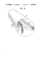
- FiG. 8 is a perspective view of yet another embodiment showing a vacuum tube emitter
- FIG. 9 is an end elevational view of the embodiment of FIG. 8;
- FIG. 10 is a partially broken top view of the embodiment of FIG. 8;
- FIG. 11 is a perspective view of another embodiment showing a flapper mirror concept
- FIG. 12 is a right side elevational view of FIG. 11;
- FIG. 13 is a top view of FIG. 11;
- FIG. 14 is a perspective view of still another embodiment showing a laser scanning technique.
- FIG. 15 is a top view of the embodiment of FIG. 14.
- FIG. 1 shows the scanning and interleaving of a cathode ray tube beam of a known television receiver.
- the beam produces an image on the screen 10 by tracing out a first field 11 during a first vertical scan, and then tracing out a second field 12 during a second vertical scan.
- the fields 11, 12, in combination, constitute a frame and the second field 12 is interleaved or interlaced within the first field 11.
- the beam starts at the upperleft most corner 13 and sweeps across horizontally (and perhaps slightly downward) to the upper rightmost corner in a generally horizontal line.
- the beam then returns to the left side following a retrace path 14 to start a new line below the previously made horizontal line.
- the beam is normally cut off or blanked so no trace appears on the screen. This process continues down the screen until field 11 is completed at the rightmost and lowest point 15. The beam then retraces to point 16 at the leftmost point on a line between the start point 13 of the first line of field 11 and the second line of that field. During this vertical retrace, the beam is also cut off.
- FIG. 2 shows the collimated video display of the present invention which can produce high resolution full color or monochrome light emitting images at high speeds from electronic signals.
- the display uses high speed light sources to generate the light.
- the sources may be lasers, laser diodes, light emitting diodes, vacuum tubes, incandescent lamps (with acoustic fluid or other suitable modulators) or other types of emitters that are capable of high speed modulation. If there are light sources of different color, they are combined and focused into light guides that produce discrete columns of parallel rays of light that are directed towards a shutter array.
- the shutter array selectively passes a horizontal section of the collimated light rays.
- the display has four fundamental components, i.e. light sources 25, light guides 20, a shutter 30, and electronic driving circuitry 21,33. Other components are required in order to realize a working device, including a power supply and signal conditioning circuitry, but these are well known.
- the four fundamental components must be coupled to each other either electrically or optically, and must be mechanically mounted in reasonably close proximity to each other.
- the light sources convert the electrical signals to light of the appropriate color or hue at video speeds.
- the first and foremost criterion for the light emitters 25 is that they must be capable of being modulated at high speed with a reasonable degree of control over the intensity.
- the light must be capable of being focused into the light guides, and therefore must reasonably approximate a point source.
- the light sources must also be a shape and size that allows them to be placed side by side for input to light guides arranged at a 0.010 inch minimum spacing between them.
- the brightness of the display is derived from the light sources.
- the maximum display output is approximately the sum of the average output of the light sources multiplied by the efficiencies of the light guides, shutter, and a ground glass diffuser surface, where used.
- the light guides e.g. collimators, convert each point light source to a vertical column of parallel light rays. Reflection is the means of control.
- the transmission medium may be air, glass or plastic and the collimators perform at up to 70% transmissivity.
- the transmission medium may use a combination of reflector types.
- a video and synchronization signal is applied to the electronics unit 21.
- the signal is separated into horizontal, vertical and video (including chromance or color) components.
- LEDs 25 Connected to electronics unit 21 are sets of three light emitting diodes (LEDs) 25. Each of these diodes emits light of a different color, i.e., red, green, yellow or blue.
- the diode sets are arranged horizontally and there is one set for each horizontal row of picture elements (pixels) of the display.
- LEDs are common in geometries of less than 0.015 inches square. The LEDs are efficient, so that high brightness can be achieved with relatively low power and a minimum of heat generation. LEDs have a lifetime of over 11 years of continuous operation, and do not degrade in storage. They are rugged and relatively insensitive to temperature changes.
- the horizontal sweep signal extracted from a television signal is applied to a circuit which has an output line for each group of LEDs (including sources of different color).
- the sweep signal preferably causes the output lines to be activated in sequence at the sweep rate.
- the cathodes of each color LED are connected to the output lines, which act to switch the cathodes of each color LED 25 to a low level.
- the anodes of the LEDs are provided with the color signals such as those corresponding to red, green and blue intensities.
- Each color LED is fed from the corresponding color signal and thus the LEDs are energized from left to right at the horizontal scan rate to emit the color dictated by the color signal and horizontal sweep signal.
- the color emitted is a color achieved by combining the outputs of two or all three of the diodes at intensities determined by the chrominance signals.
- Light 26 from the LEDs 25 is focused or channeled into respective collimators 20, one for each set of LEDs or column of pixels.
- the light enters through an entrance, e.g. lens surface 24, and diverges by internal reflection off mirrored surfaces 28,29 on the collimator edges as shown in FIGS. 2-4.
- the LEDs may be focused into the collimators simply by placing them close to the collimator inputs with the maximum beam point aimed properly.
- the LEDs may have small reflectors to focus the light into the collimator input.
- the reflectors may also gather light that is emitted from the sides of the LEDs that otherwise would have been lost.
- These reflectors may be integral with the LEDs or even made of the adhesive that bonds them to their substrate.
- the copper bonding pads of a hybrid may be "dimpled" to form a reflector prior to the LED being mounted.
- the conductive adhesive or solder may also be formed into a reflector in a similar manner.
- An oil, gel, or other liquid may be used to focus more of the light from the sources to the collimators.
- the fluid acts as a lens and mirror keeping the light output from interfering with the neighboring sources and directing it to the input of the respective collimator.
- the fluid could be applied to individual units or to the entire assembly, depending on its properties and the construction of the collimators themselves.
- the LEDs may be situated within a small cavity at the input to the collimator. The cavity would then be filled with material to secure the LED. This coupling technique is very effective at preventing interference and providing excellent optical coupling.
- More than one LED may be used for each color of each collimator to increase the brightness of the display.
- the LEDs would be connected in series, and the collimators would be made to accept the input.
- the drive circuitry would not need much, if any, modification to drive multiple LEDs.
- collimator sets with single or multiple LEDs can be used.
- One system could be used for the lower portion of the display and one for the upper portion, in a two block display.
- the collimators would be aligned vertically and in abutment, to eliminate any gaps. This would involve one set of collimators and LEDs for each section.
- the multiple collimator sets greatly increase the contrast as well as the brightness of the display, because those sections not being horizontally addressed could be turned off.
- the amount of light from each LED would be concentrated in a smaller area of the display, and therefore would be brighter.
- Mirrored surface 28 of the collimator is a convex parabolic and mirrored surface 29 is a concave hyperbolic, so that the light rays 26' reflecting off the mirrored surface 29 emerge through the front surface 27 of the collimator parallel to each other and perpendicular to the front surface 27.
- the mirrored surfaces are arranged in an offset relationship. After emerging from the front surface 27, the light rays reach the shutter assembly 30 (FIG. 2).
- the side surfaces 23 of the collimators act to reflect or refract the light from the source as the light travels in the core 26 (FIG. 5). This acts to keep the light from neighboring collimators from interfering and permits utilization of as much of the output light as possible.
- the collimators may be made of glass or plastic material, which is available in a variety of different indices of refraction with excellent optical characteristics. They are shaped, polished, and aluminized to form the mirrors on surfaces 28,29. Instead of a parabolic and hyperbolic pair, the mirrors can be circular or elliptical.
- the collimators can be injection molded from plastic or molded of high quality glass.
- FIGS. 3-5 show the details of the collimator.
- the collimator is thin (e.g., less than 0.01 inches) including its core 26 and cladding 23 which are sandwiched together.
- the core 26 is formed to allow for the transmission of light without much loss or dispersion.
- the cladding 23 may be made out of a reflective material.
- the cladding 23 may alternatively be made of a transparent material. However, if the cladding 23 and core 26 are both transparent, they should have different indices of refraction. If the cladding is made denser than that of the core 26, light is prevented from escaping through the cladding 23 by refraction. This also prevents light from outside the cladding from interfering with the light being collimated.
- the collimator both cladding and core, may be made of a solid transparent material, such as plastic or glass material.
- a solid transparent material the core 26 helps to support the mirrored surfaces 28,29.
- the core 26 could be an empty space, gas or liquid.
- Each of the elongated shutter apertures 31 is preferably a negative transmissive type of liquid crystal, but the LCD may be of any type.
- the apertures 31 become transparent with the application of a voltage to the aperture electrode 32 with a negative transmissive type.
- the aperture speed requirement of the preferred embodiment is 100uS at a minimum in order to display 500 lines of non interleaved display at 30Hz.
- Ncap type crystal may be used to increase speed, lower cost, increase the brightness, and increase the size of the active display. However, this type crystal provides lesser contrast. Thus, a high resolution display of pixels is achieved.
- the transmissivity of the shutter assembly in the on and off modes is an important factor in determining the performance of the system. Also, the contrast of the system must be lower than the contrast of the shutter device, making single layer liquid crystal elements minimally suitable for this application. An ideal contrast ratio would approach 100:1, usable contrast ratios would be in the 5 to 10:1 range.
- the contrast of the display is highly dependent on the characteristics of the shutter performance. The slower the aperture movement, or longer the transition time, the lower the overall display contrast.
- the driving circuitry will be taxed to accommodate a display with poor shutter performance.
- the shutter system must be manufacturable in a large size with a variety of aspect ratios.
- the apertures must be capable of being closely spaced, and the actuation means must not interfere with the transmission of the light.
- the LCD could be a smectic C-type for very high speed displays and for large glass. Manufacturing LCD panels is done with laser sealed edges and feed throughs for connection to the back. These panels may be combined to produce very large displays in a modular fashion.
- the LCD may use transparent metal electrodes to improve speed, or it may use highly conductive metal connectors that run the entire length of the apertures.
- a viewer may look at the shutter directly. If the light rays emerge parallel to each other, then a diffuser screen or scattering plate is placed in front of the LCD shutter assembly for a viewer to look through. Etched glass or panel frosting may be used for the viewer to look through to improve the viewing angle.
- the shutter electronics 33 drives the shutter assembly with pulses.
- the pulses open and close the shutter apertures 31 to modulate the collimated light according to the vertical scan rate of the video signal.
- the spaces between the apertures is minimized to enhance clarity. This modulation may be done, for instance, sequentially, by every other one, or in any desired manner to maximize contrasts.
- FIG. 6 shows a block diagram of the electronic circuitry which processes a composite video signal 43 into signals suitable for the LEDs 25 and the LCD shutter assembly 30.
- the driving circuitry includes a mixture of analog and logic circuits. The logic is designed so that a number of different driving sequences can be employed. The power requirements and the shutter performance will determine the complexity of the driving circuitry. Since the speed of the vertical sweep is low, standard transistor-to-transistor logic (TTL) circuitry to control may be used for that application.
- TTL transistor-to-transistor logic
- the horizontal control circuitry operates at very high speeds and power levels.
- the efficiency and type of light emitter plays a large role in determining the type and complexity of the actual circuitry. LED emitters require large current capacity in both the switching elements as well as the analog counterparts. They also require extra circuitry in order to generate persistence or other special control techniques for improved light output.
- This type of circuitry is most easily constructed on a single chip by known custom technology or else mounted on a semiconducting disc with some components silk screened onto aluminum by known hybrid custom technology.
- the composite video signal 43 is first fed into a synchronization separator (sync circuit) 51 which separates the input signal into a vertical pulse signal 41, a horizontal pulse signal 42 and a video intensity signal 44 (chroma and luminance ⁇ .
- a synchronization separator sync circuit 51 which separates the input signal into a vertical pulse signal 41, a horizontal pulse signal 42 and a video intensity signal 44 (chroma and luminance ⁇ .
- the video intensity signal 44 is fed to video amplifiers 52, which convert the chroma and luminance signals into amplitudes corresponding to red R, green G and blue B intensities.
- the video amplifiers 52 convert the intensity signals into current drive signals for each anode of each color LED, which signals appear on lines 47.
- the LED drive circuitry is designed to drive a high capacitance load.
- the horizontal clock circuit 53 is triggered by the horizontal pulse signal 42 from the sync circuit 51.
- This horizontal clock circuit 53 divides the duration between horizontal sync pulses 42 into a number of sub-intervals corresponding to the number of groups of LEDs, and provides an appropriate horizontal scan frequency. This corresponds to the horizontal resolution.
- the clock frequency is adjustable to allow for horizontal sizing requirements, i.e. by means of a change in oscillator frequency. Horizontal centering is not required because the image must start from the left side as is governed by the physical position of the LEDs and the trigger pulse from the sync circuit 51.
- the clock pulses from the horizontal clock circuit 53 are counted by a counter circuit 54, which decodes the counted signal to activate any desired number of decode signal lines 45 leading to the cathodes for groups of LEDs 25.
- the number of decode signal lines may correspond to the number of groups of LEDs.
- the decoded signals are buffered to drive the cathodes of the LEDs 25.
- the buffering is done with open collector transistors so as to electrically isolate the LEDs entirely from the rest of the circuit when they are not activated.
- An LED becomes activated when the decoded signal is present on the cathode and a video signal is simultaneously present on the anode.
- Video buffers i.e. blue 73, green 74 and red 75, of the video amplifiers 52 of FIG. 6, transmit video signals of sufficient magnitude for activating respective LEDs 25 at the anode side 25B.
- Driver transistors 71 which receive the decoded horizontal signals 72 of circuit 54 in FIG. 6 and activate the LEDs 25 at their cathode side 25A.
- Limiting resistors 59 are provided to avoid burning out the LED diodes 25 due to excess current.
- Decoupling diodes 70 are provided to effectively electrically isolate respective LEDs from the circuit when they are no longer being activated through the driver transistors. Holding capacitors 56 provide persistence of illumination of the LEDs 25 after electrical isolation takes place.
- Holding capacitors 56 keep the LEDs "on” for a short period of time after the electrical isolation takes place so as to enable the colored light from the group of LEDs to be delivered to the viewer.
- the holding capacitors 56 allow the collimated video display to more closely approximate the look of a typical CRT and to increase the light output of the display. The capacitor will not interfere with the operation of the other LEDs because of the open collector drive system. Only one holding capacitor 56 is shown in FIG. 6 for the sake of clarity, but there is actually one for each LED as indicated in FIG. 7.
- the vertical clock circuit 57 (FIG. 6) is very similar to the horizontal clock circuit 53. It is triggered by the vertical signal pulses from the sync circuit 51. A clock in circuit 57 divides up the vertical sync pulse 41 by the number of apertures in the LCD shutter assembly 10 to provide a clocked frequency of vertical pulses. This corresponds to the vertical resolution. The vertical clock frequency can be adjusted to allow for vertical sizing. A vertical centering control is not required because the signal and the image must start from the top and the physical location of the shutter apertures 31 is fixed.
- These clocked vertical pulses are counted by a counter and decoder circuit 58 which counts the number of pulses and decodes the counted signal in order to sequentially activate, at any one time, only one of the total number of vertical decoded signal lines.
- These signal lines correspond to the apertures 31 in the LCD shutter assembly or may correspond to more than one line to provide for overlay or interleaving of scan lines.
- the vertical decoded signals are buffered to directly drive the apertures 31.
- the buffering is achieved with an active totem pole transistor arrangement which provides the greatest speed for opening and closing the apertures 31.
- the collimated video display is a flat, lightweight, low power, high speed, high resolution, full color display which utilizes a combination of liquid crystal displays, optical collimators and light emitting diodes.
- the slower, vertical sweep in a typical TV screen is accomplished with the LCD elements and the higher rate horizontal sweep is accomplished by switching LED elements.
- the optical collimators expand the light from the LEDs to the vertical size of the shutter assembly or display.
- Electronic circuitry conditions a normal television composite video signal to provide the signals used by the LED and LCD elements of this display.
- a sequential horizontal sweep of the display is created.
- a sequential vertical sweep of the display is created.
- a full color or monochrome, flat screen display is formed from a conventional broadcast television signal.
- the switching need not be sequential; rather any desired order can be used (e.g. to improve contrast).
- the present invention has many intrinsic advantages over CRTs.
- the pixel addressing mechanism for the CRT is serial, and requires retrace blanking and delays.
- the present device addressing mechanism is pseudorandom, and is compatible with conventional enhancement methodologies. It can also use the blanking periods for persistence in keeping the LEDs on to increase the overall light output.
- the shutter apertures are liquid crystal, and therefore have a certain delay before the crystal actually changes.
- the liquid crystal structure if it is of the twisted-nematic type, mechanically twists when it is changing state, and the transmissivity of the aperture changes with it. It is possible to use this latency to increase the brightness without a sacrifice in resolution or speed.
- the present arrangement is capable of random addressing of apertures or lines, and pixels (LED groups) within that line. It is also possible to open more than one aperture at a time.
- the LEDs may be driven with circuitry that stores information for a line. The energy representing this information is then discharged into the LED devices for a period, determined by the circuitry, during which the entire shutter aperture is open. The stored information is then overwritten during the next access period. Information passed to the next aperture down in the vertical shutter could cause distortion, but it can be kept at a minimum. This type of distortion results in a lower contrast display, not lower resolution.
- the LEDs may be driven with circuitry that will operate them past their "linear” region in LED burst modes.
- the "linear region” is represented by a flat area on a curve plot of input power versus output power for LEDs. LEDs require that a threshold voltage level be reached first before there will be any light power output. When the threshold is reached, there is a sudden surge in light output power. At the opposite extreme, there comes a point at which the amount of output power tapers off despite steady increases in input power. In between these two extremes is the “linear region”.
- the light output of an LED is close to proportional to the drive current within the range of the "linear region”. This range is from almost zero to near the rated average current of the device.
- the LED can be operated at higher currents with lower duty cycles in order to deliver maximum brightness.
- the circuitry can be tailored to provide a reasonably linear light output. However, in this mode, the life of the LED is decreased and the spectral output is changed, but they may be within tolerable limits.
- Two apertures may be opened at the same time for twice the aperture sweep duration. This may be accomplished by alternating each frame to simulate interleaving, and at the same time the intensity can be increased without loss of contrast or resolution.
- the shutter drive circuitry requires the independent and individual drive capability for this function.
- Shutter overlap using the inherent latency of the crystal can be exploited through the use of delay and prefiring.
- the shutter apertures may be opened in a wave-like manner. This provides greater brightness with a sacrifice of contrast and color purity.
- a triple aperture method uses a very slow time base to open an aperture during normal or interleaved operation to provide greater brightness. This results in a loss of resolution, but not contrast.
- Very high brightness light sources allow multiple layer shutter assemblies to be used for greater contrast. This technique employs two identical shutter assemblies that are controlled with the same circuitry. The brightness would be reduced considerably, but the contrast could be increased by a great amount.
- the potential performance of the present system may be enhanced by changing the electronic driving techniques.
- the speed, contrast and brightness may all be improved by changing the way the shutter apertures and light sources are controlled.
- a vacuum tube may be used as the light source.
- the tube consists of three indirectly heated cathodes, one grid for each color, an anode area, and three colored phosphor coatings running the length of the tube.
- the tube can be as small as 1/4 of an inch in diameter, and from one to three feet in length. This type of emitter offers lower cost and higher brightness than LEDs, but would be less rugged, have a shorter life, and be more difficult to interface with the collimators.
- a vacuum tube light emitter is much easier to drive because the current is only required by the analog section of the circuit.
- the switching section is driven with very low power devices. Persistence is achieved with the proper selection of existing phosphor technology. Custom or semicustom integrated circuit fabrication methods are most suited for the vacuum tube drive circuitry.
- FIGS. 8-10 show a tri-color light emitting vacuum tube with multiple control grids 104 oriented in a matrix pattern with respect to the three cathodes 101 with heaters.
- Connectors 102 connect the heaters in the cathodes with outside circuitry (not shown) for varying the intensity of the electron beams eminating from the cathodes with respect to video chromance signals 44 of FIG. 6.
- the tube includes a glass envelope 100 enclosing an evacuated area.
- the three cathodes 101 are associated with the three phosphor coatings 108, each phosphor coating providing a different color of light when struck by electrons from the respective cathodes.
- a focus electrode and ion trap 103 is provided to allow only narrow beams of electrons, e.g. one for each collimator, to pass through its apertures.
- control grids 104 By controlling the activation of the control grids 104, only selected electron beams are permitted to pass by the control grid.
- Each control element of the control grid is activated to set up an opposite charge to block the electron beams in synchronism with horizontal sync pulses 42 of FIG. 6.
- a suppressor grid 106 is activated to slow the flow of electrons toward the anode coating 107 to ensure that the electrons impinge on the respective phosphor coatings 108 with the proper energy to give the desired intensity set by the luminescence signal.
- the control grid 104 is arranged in correspondence with the collimators (not shown ⁇ so that illuminating selected areas of the phosphor coating will permit light to enter only corresponding collimators. Varying the flow of the electrons emitted from the cathodes (e.g. in response to video intensity signals 44 of FIG. 6) affects the type of colors that will be achieved from the excited phosphor coating; controlling the control grid selectively will determine which areas on the phosphor coatings will be struck by the electrons in alignment with desired collimators (e.g. in response to horizontal sync pulses 42 of FIG. 6).
- FIGS. 11-13 depict an embodiment employing flapper mirrors 80.
- These flapper mirrors may be made of flexible polyvinylfluoride sheets. Flapper mirrors reduce the number of LEDs required because a flapper mirror can focus light from one group of LEDs 25 (e.g. red, blue, green) into each of a set of collimators 84 individually.
- the mirrors may be of the piezoelectric film type that are driven to move in response to electrical signals from separate drive circuitry that is synchronized with the LED drive of FIG. 6.
- FIGS. 11-13 show a flapper mirror 80 held in a mirror holder 81 that has an electrical connector.
- the piezoelectric flapper mirror 80 is in motion for sweeping the light rays 26' across the width of the display of collimators 84.
- Each collimator 84 has a hyperbolic mirrored surface 28 and parabolic mirrored surface 29 as in the embodiment of FIG. 2.
- Each collimator also has a differently angled cut away area 82 at each of the respective entrance surfaces to accommodate entry of the light rays 26' into the collimators 84 after reflection off the flapper mirrors 80 so that the light rays will refract axially along the length of the collimator toward the mirrored surface 28. Together, the cut away areas appear to form the outline of an arc.
- a rotating scanning type mirror may also be used. It is rotated so as to reflect light (e.g. from lasers) to the cut away areas 82 of the collimators, respectively, so that the light sweeps across the width of the display.
- FIGS. 14 and 15 show a rotating scanning type mirror which is used for lasers, but which does not employ collimators.
- Modulated lasers 90 emit colored light beams 95 at a rotating scanning mirror 91.
- the intensity of the light beam varies in response to video chromance signals, e.g. in a manner similar to varying the light intensity of the LEDs in response to video chromance signals 44 of FIG. 6.
- the light beams 95 are vertically diverged as they leave each laser (e.g. by diverging the light with lenses at the exit of each laser).
- the divergent light beams from the lasers mix with each other to provide a desired color intensity of light which is then reflected off the rotating scanning mirror 91 to strike a shutter 93 located across the height of the display.
- the mirror 91 is rotated by a motor 94 driven in response to separate electronic circuitry that is synchronized with the LED drive of FIG. 6. By so driving the motor 94 to rotate the mirror 91 (e.g. with respect to horizontal pulses 42 of FIG. 6), the light will sweep across the width of the display. Light passing through the shutter 93 emerges through etched glass 92, which diffuses the light. FIG. 15 shows the mirror 91 superimposed on itself in three different positions during rotation, causing the laser light to strike the shutter at three respective areas across its entire height.
- the rotatable mirror 91 is shown extending vertically to a height of the shutter, but other orientations and configurations for the mirror are also possible (e.g. angling the mirror). Three lasers 90 are shown, each emitting a different color (e.g. red, blue, green), but a single laser could be used instead to produce a monochrome display.
- the shutter 93 is the same as the shutter assembly 30 of the embodiment of FIG. 2 and is controlled in a similar manner.
- Non linear optical transistors may be used as shutters and also as valves for the collimators in the case of a single light source.
- the incident light dependent devices are driven with some of the unmodulated primary light source, or with other secondary sources.
- the entire assembly may be grown from silicon with a variety of doping stages.
- the shutter, collimators, LEDs and driving circuitry are formed by a combination of processes from a single crystal block of silicon. The crystal is very large.
- the collimators may be formed by altering the crystalline structure of the silicon to change its index of refraction at specific locations by ion bombardment, x-ray exposure, or with laser light.
- the shutter aperture pattern could be masked directly onto the front of the block.
- a face plate would contain the liquid.
- LEDs may be doped into the back of the collimator structure.
- the crystal would be exposed to a variety of doping gasses and compounds during growth.
Abstract
Description
Claims (53)
Priority Applications (3)
| Application Number | Priority Date | Filing Date | Title |
|---|---|---|---|
| US07/315,734 US4978952A (en) | 1989-02-24 | 1989-02-24 | Flat screen color video display |
| PCT/US1990/001068 WO1990010357A1 (en) | 1989-02-24 | 1990-02-26 | Video display system |
| AU51826/90A AU5182690A (en) | 1989-02-24 | 1990-02-26 | Video display system |
Applications Claiming Priority (1)
| Application Number | Priority Date | Filing Date | Title |
|---|---|---|---|
| US07/315,734 US4978952A (en) | 1989-02-24 | 1989-02-24 | Flat screen color video display |
Publications (1)
| Publication Number | Publication Date |
|---|---|
| US4978952A true US4978952A (en) | 1990-12-18 |
Family
ID=23225817
Family Applications (1)
| Application Number | Title | Priority Date | Filing Date |
|---|---|---|---|
| US07/315,734 Expired - Fee Related US4978952A (en) | 1989-02-24 | 1989-02-24 | Flat screen color video display |
Country Status (3)
| Country | Link |
|---|---|
| US (1) | US4978952A (en) |
| AU (1) | AU5182690A (en) |
| WO (1) | WO1990010357A1 (en) |
Cited By (117)
| Publication number | Priority date | Publication date | Assignee | Title |
|---|---|---|---|---|
| US5083120A (en) * | 1990-02-23 | 1992-01-21 | Bell Communications Research, Inc. | Flat panel display utilizing leaky lightguides |
| US5138309A (en) * | 1990-04-03 | 1992-08-11 | Aura Systems, Inc. | Electronic switch matrix for a video display system |
| US5144416A (en) * | 1990-10-10 | 1992-09-01 | Eastman Hart | Video display and imaging devices having liquid crystal scanning |
| US5317436A (en) * | 1990-12-31 | 1994-05-31 | Kopin Corporation | A slide assembly for projector with active matrix moveably mounted to housing |
| US5359345A (en) * | 1992-08-05 | 1994-10-25 | Cree Research, Inc. | Shuttered and cycled light emitting diode display and method of producing the same |
| US5381502A (en) * | 1993-09-29 | 1995-01-10 | Associated Universities, Inc. | Flat or curved thin optical display panel |
| US5396304A (en) * | 1990-12-31 | 1995-03-07 | Kopin Corporation | Slide projector mountable light valve display |
| US5416514A (en) * | 1990-12-27 | 1995-05-16 | North American Philips Corporation | Single panel color projection video display having control circuitry for synchronizing the color illumination system with reading/writing of the light valve |
| US5428366A (en) * | 1992-09-09 | 1995-06-27 | Dimension Technologies, Inc. | Field sequential color illumination system for liquid crystal display |
| WO1995020811A1 (en) * | 1994-01-31 | 1995-08-03 | Sdl, Inc. | Laser illuminated display system |
| US5467154A (en) * | 1992-02-20 | 1995-11-14 | Kopin Corporation | Projection monitor |
| US5475514A (en) * | 1990-12-31 | 1995-12-12 | Kopin Corporation | Transferred single crystal arrayed devices including a light shield for projection displays |
| US5479187A (en) * | 1994-02-23 | 1995-12-26 | Chunghwa Picture Tubes, Ltd. | Vertically scanned narrow light beam source for LCD display |
| US5566370A (en) * | 1994-11-03 | 1996-10-15 | Lockheed Martin Corporation | Simulation display system |
| US5597518A (en) * | 1992-04-10 | 1997-01-28 | Silicon Video Corporation | Method for producing self supporting flat video display |
| US5613751A (en) * | 1995-06-27 | 1997-03-25 | Lumitex, Inc. | Light emitting panel assemblies |
| EP0771673A1 (en) | 1995-11-01 | 1997-05-07 | Eastman Kodak Company | Method of making a color filter array element |
| US5664859A (en) * | 1994-01-03 | 1997-09-09 | Kopin Corporation | Projection display docking system |
| US5692820A (en) * | 1992-02-20 | 1997-12-02 | Kopin Corporation | Projection monitor |
| US5724062A (en) * | 1992-08-05 | 1998-03-03 | Cree Research, Inc. | High resolution, high brightness light emitting diode display and method and producing the same |
| US5748164A (en) * | 1994-12-22 | 1998-05-05 | Displaytech, Inc. | Active matrix liquid crystal image generator |
| US5757348A (en) * | 1994-12-22 | 1998-05-26 | Displaytech, Inc. | Active matrix liquid crystal image generator with hybrid writing scheme |
| US5796377A (en) * | 1990-04-03 | 1998-08-18 | Aura Systems, Inc. | Video display system having an electronic switch matrix for controlling an M×N array of piezoelectric members |
| US5812105A (en) * | 1996-06-10 | 1998-09-22 | Cree Research, Inc. | Led dot matrix drive method and apparatus |
| US5818400A (en) * | 1996-04-09 | 1998-10-06 | International Resource Management Inc. | Display device using intersecting optical beams |
| US5844540A (en) * | 1994-05-31 | 1998-12-01 | Sharp Kabushiki Kaisha | Liquid crystal display with back-light control function |
| US5895115A (en) * | 1996-01-16 | 1999-04-20 | Lumitex, Inc. | Light emitting panel assemblies for use in automotive applications and the like |
| US5940163A (en) * | 1994-07-19 | 1999-08-17 | Electro Plasma Inc. | Photon coupled color flat panel display and method of manufacture |
| US5975711A (en) * | 1995-06-27 | 1999-11-02 | Lumitex, Inc. | Integrated display panel assemblies |
| US6160596A (en) * | 1999-12-20 | 2000-12-12 | Delphi Technologies, Inc. | Backlighting system for a liquid crystal display unit |
| US6288700B1 (en) * | 1994-05-09 | 2001-09-11 | Hiroki Mori | Light emitting flat panel device which uses light guide routes to directly send light into a matrix of electronic shutters |
| EP1182633A2 (en) * | 2000-08-16 | 2002-02-27 | Gateway, Inc. | Display Assembly |
| US6414652B1 (en) * | 1997-12-19 | 2002-07-02 | Rohm Co., Ltd. | Color image reader |
| US6448951B1 (en) * | 1998-05-11 | 2002-09-10 | International Business Machines Corporation | Liquid crystal display device |
| US20020141174A1 (en) * | 1995-06-27 | 2002-10-03 | Jeffery R. Parker | Light emitting panel assemblies |
| US20020180678A1 (en) * | 1998-04-03 | 2002-12-05 | Kabushiki Kaisha Toshiba | Image display system and image display methods |
| US20030035221A1 (en) * | 1999-12-16 | 2003-02-20 | Kazuya Yoneyama | Illumination optical system and projection type image display apparatus using the same |
| US6628254B1 (en) * | 1999-03-31 | 2003-09-30 | Advanced Display Inc. | Display device and interface circuit for the display device |
| US20040071417A1 (en) * | 2002-10-09 | 2004-04-15 | Veligdan James T. | Display panel having dual directional diffusion |
| WO2005020004A2 (en) * | 2003-08-19 | 2005-03-03 | Shivji Shiraz M | Method and apparatus for light emitting devices based display |
| US20050088403A1 (en) * | 1998-09-03 | 2005-04-28 | Semiconductor Energy Laboratory Co., Ltd. | Electronic device with liquid crystal display |
| US20050122591A1 (en) * | 1999-02-23 | 2005-06-09 | Parker Jeffery R. | Light redirecting films and film systems |
| US20060114172A1 (en) * | 2004-11-26 | 2006-06-01 | Giotti, Inc. | Method and apparatus for LED based modular display |
| US20060132423A1 (en) * | 2003-06-06 | 2006-06-22 | Travis Adrian R L | Scanning backlight for flat-panel display |
| US7108414B2 (en) * | 1995-06-27 | 2006-09-19 | Solid State Opto Limited | Light emitting panel assemblies |
| US20060256256A1 (en) * | 2005-05-10 | 2006-11-16 | Samsung Electronics Co., Ltd. | Backlight unit and liquid crystal display employing the same |
| US20060262079A1 (en) * | 2005-05-19 | 2006-11-23 | Samsung Electronics Co., Ltd. | Backlight unit and liquid crystal display employing the same |
| US20070019130A1 (en) * | 2005-07-22 | 2007-01-25 | Industrial Technology Research Institute | Liquid crystal display |
| US20070052636A1 (en) * | 2002-02-09 | 2007-03-08 | Kalt Charles G | Flexible video displays and their manufacture |
| US20070118593A1 (en) * | 2004-07-26 | 2007-05-24 | Shiraz Shivji | Positioning system and method for LED display |
| US20070229453A1 (en) * | 1999-03-23 | 2007-10-04 | Sukekazu Aratani | Liquid Crystal Display Apparatus |
| US20070247871A1 (en) * | 2006-04-21 | 2007-10-25 | Samsung Electro-Mechanics Co., Ltd. | Backlight unit for liquid crystal display device |
| US20070285392A1 (en) * | 2006-06-07 | 2007-12-13 | Boon Kheng Lee | Utilizing an internal reflection surface to reflect and collimate sidelight in an optical navigation device |
| US7367705B2 (en) | 2004-11-04 | 2008-05-06 | Solid State Opto Limited | Long curved wedges in an optical film |
| US7385574B1 (en) | 1995-12-29 | 2008-06-10 | Cree, Inc. | True color flat panel display module |
| US20080204397A1 (en) * | 2007-02-22 | 2008-08-28 | Hyeon-Yong Jang | Backlight device and liquid crystal display device having the same |
| US7448775B2 (en) | 1999-02-23 | 2008-11-11 | Solid State Opto Limited | Transreflectors, transreflector systems and displays and methods of making transreflectors |
| US20090052046A1 (en) * | 2002-03-21 | 2009-02-26 | Lumus Ltd. | Light guide optical device |
| US20090073348A1 (en) * | 2007-09-17 | 2009-03-19 | Young Optics Inc. | Display and backlight module thereof |
| US7540644B1 (en) * | 2007-05-03 | 2009-06-02 | Laughing Rabbit, Inc. | LCD optic shutter |
| EP2131099A1 (en) * | 2007-03-20 | 2009-12-09 | Panasonic Corporation | Surface illumination device and liquid crystal display using the same |
| US20110254032A1 (en) * | 2010-04-20 | 2011-10-20 | Avago Technologies Ecbu Ip (Singapore) Pte. Ltd. | Electronic Assembly |
| DE102010018119A1 (en) * | 2010-04-24 | 2011-10-27 | Hella Kgaa Hueck & Co. | Optical element for lighting device of vehicle, has body, which is formed of transparent material in one-piece and has multiple bounding surfaces |
| US8130439B2 (en) | 1994-12-22 | 2012-03-06 | Micron Technology, Inc. | Optics arrangements including light source arrangements for an active matrix liquid crystal generator |
| DE102012102105A1 (en) * | 2011-03-30 | 2012-10-04 | Visteon Global Technologies, Inc. | collimator |
| US8322905B2 (en) | 1999-02-23 | 2012-12-04 | Rambus International Ltd. | Edgelit panel with curvilinear light extracting deformities |
| US8462292B2 (en) | 2008-07-31 | 2013-06-11 | Rambus Delaware Llc | Optically transmissive substrates and light emitting assemblies and methods of making same, and methods of displaying images using the optically transmissive substrates and light emitting assemblies |
| US8755059B2 (en) | 2011-11-08 | 2014-06-17 | Taishita LLC | Portable multiuse projector with fiber optic projection |
| US8827347B2 (en) | 2010-04-23 | 2014-09-09 | Magna Mirrors Of America, Inc. | Vehicle window with shade |
| US9539883B2 (en) | 2010-04-23 | 2017-01-10 | Magna Mirrors Of America, Inc. | Window with shade |
| WO2018154564A1 (en) * | 2017-02-22 | 2018-08-30 | Real View Imaging Ltd. | Pupil tracking in an image display system |
| US20190011627A1 (en) * | 2016-12-27 | 2019-01-10 | HKC Corporation Limited | Backlight module and display apparatus thereof |
| US10261321B2 (en) | 2005-11-08 | 2019-04-16 | Lumus Ltd. | Polarizing optical system |
| US10302835B2 (en) | 2017-02-22 | 2019-05-28 | Lumus Ltd. | Light guide optical assembly |
| US10437031B2 (en) | 2016-11-08 | 2019-10-08 | Lumus Ltd. | Light-guide device with optical cutoff edge and corresponding production methods |
| US10481319B2 (en) | 2017-03-22 | 2019-11-19 | Lumus Ltd. | Overlapping facets |
| US10520731B2 (en) | 2014-11-11 | 2019-12-31 | Lumus Ltd. | Compact head-mounted display system protected by a hyperfine structure |
| US10551544B2 (en) | 2018-01-21 | 2020-02-04 | Lumus Ltd. | Light-guide optical element with multiple-axis internal aperture expansion |
| US10564417B2 (en) | 2016-10-09 | 2020-02-18 | Lumus Ltd. | Aperture multiplier using a rectangular waveguide |
| US10649214B2 (en) | 2005-02-10 | 2020-05-12 | Lumus Ltd. | Substrate-guide optical device |
| US10739513B2 (en) | 2018-08-31 | 2020-08-11 | RAB Lighting Inc. | Apparatuses and methods for efficiently directing light toward and away from a mounting surface |
| US10788791B2 (en) | 2016-02-22 | 2020-09-29 | Real View Imaging Ltd. | Method and system for displaying holographic images within a real object |
| US10795316B2 (en) | 2016-02-22 | 2020-10-06 | Real View Imaging Ltd. | Wide field of view hybrid holographic display |
| US10794110B2 (en) | 2018-07-06 | 2020-10-06 | Guardian Glass, LLC | Electric potentially-driven shade with perforations, and/or method of making the same |
| US10801679B2 (en) | 2018-10-08 | 2020-10-13 | RAB Lighting Inc. | Apparatuses and methods for assembling luminaires |
| US10801258B2 (en) | 2018-07-06 | 2020-10-13 | Guardian Glass, LLC | Flexible dynamic shade with post-sputtering modified surface, and/or method of making the same |
| US10809528B2 (en) | 2014-04-23 | 2020-10-20 | Lumus Ltd. | Compact head-mounted display system |
| US10858884B2 (en) | 2018-07-06 | 2020-12-08 | Guardian Glass, LLC | Electric potentially-driven shade with improved coil strength, and/or method of making the same |
| US10871027B2 (en) | 2018-07-06 | 2020-12-22 | Guardian Glass, LLC | Electric potentially-driven shade with CIGS solar cell, and/or method of making the same |
| US10877437B2 (en) | 2016-02-22 | 2020-12-29 | Real View Imaging Ltd. | Zero order blocking and diverging for holographic imaging |
| US10876349B2 (en) | 2018-07-06 | 2020-12-29 | Guardian Glass, LLC | Electro-polymeric shade for use at elevated temperature and/or methods of making the same |
| US10895679B2 (en) | 2017-04-06 | 2021-01-19 | Lumus Ltd. | Light-guide optical element and method of its manufacture |
| US10895102B2 (en) | 2018-07-06 | 2021-01-19 | Guardian Glass, LLC | Electric potentially-driven shade with improved electrical connection between internal shade and external power source, and/or method of making the same |
| US10914114B2 (en) | 2018-07-06 | 2021-02-09 | Guardian Glass, LLC | Electric potentially-driven shade including shutter supporting surface-modified conductive coating, and/or method of making the same |
| US10927592B2 (en) | 2018-07-06 | 2021-02-23 | Guardian Glass, LLC | Electric potentially-driven shade with surface-modified polymer, and/or method of making the same |
| US11174676B2 (en) | 2020-02-03 | 2021-11-16 | Guardian Glass, LLC | Electric potentially-driven shade with improved shade extension control, and/or associated methods |
| US11210972B1 (en) | 2020-12-23 | 2021-12-28 | New Visual Media Group, L.L.C. | Optical shutter and display panel |
| US11421470B2 (en) | 2020-02-17 | 2022-08-23 | Guardian Glass, LLC | Coil skew correction techniques for electric potentially-driven shade, and/or associated methods |
| US11428040B2 (en) | 2020-02-03 | 2022-08-30 | Guardian Glass, LLC | Electrostatic latching stop bar for dynamic shade, and/or associated methods |
| US11448816B2 (en) | 2019-01-24 | 2022-09-20 | Lumus Ltd. | Optical systems including light-guide optical elements with two-dimensional expansion |
| US11523092B2 (en) | 2019-12-08 | 2022-12-06 | Lumus Ltd. | Optical systems with compact image projector |
| US11526003B2 (en) | 2018-05-23 | 2022-12-13 | Lumus Ltd. | Optical system including light-guide optical element with partially-reflective internal surfaces |
| US11543583B2 (en) | 2018-09-09 | 2023-01-03 | Lumus Ltd. | Optical systems including light-guide optical elements with two-dimensional expansion |
| US11561335B2 (en) | 2019-12-05 | 2023-01-24 | Lumus Ltd. | Light-guide optical element employing complementary coated partial reflectors, and light-guide optical element having reduced light scattering |
| US11630260B2 (en) | 2020-05-24 | 2023-04-18 | Lumus Ltd. | Production method and corresponding structures of compound light-guide optical elements |
| US11634942B2 (en) | 2020-02-03 | 2023-04-25 | Guardian Glass, LLC | Electric potentially-driven shade with electrostatic shade retraction, and/or associated methods |
| US11644676B2 (en) | 2020-09-11 | 2023-05-09 | Lumus Ltd. | Image projector coupled to a light guide optical element |
| US11663937B2 (en) | 2016-02-22 | 2023-05-30 | Real View Imaging Ltd. | Pupil tracking in an image display system |
| US11714316B2 (en) | 2017-09-20 | 2023-08-01 | New Visual Media Group, L.L.C. | Highly reflective electrostatic shutter display |
| US11789264B2 (en) | 2021-07-04 | 2023-10-17 | Lumus Ltd. | Display with stacked light-guide elements providing different parts of field of view |
| US11796729B2 (en) | 2021-02-25 | 2023-10-24 | Lumus Ltd. | Optical aperture multipliers having a rectangular waveguide |
| US11822088B2 (en) | 2021-05-19 | 2023-11-21 | Lumus Ltd. | Active optical engine |
| US11860369B2 (en) | 2021-03-01 | 2024-01-02 | Lumus Ltd. | Optical system with compact coupling from a projector into a waveguide |
| US11885966B2 (en) | 2019-12-30 | 2024-01-30 | Lumus Ltd. | Optical systems including light-guide optical elements with two-dimensional expansion |
| US11886008B2 (en) | 2021-08-23 | 2024-01-30 | Lumus Ltd. | Methods of fabrication of compound light-guide optical elements having embedded coupling-in reflectors |
| US11914187B2 (en) | 2019-07-04 | 2024-02-27 | Lumus Ltd. | Image waveguide with symmetric beam multiplication |
| US11914161B2 (en) | 2019-06-27 | 2024-02-27 | Lumus Ltd. | Apparatus and methods for eye tracking based on eye imaging via light-guide optical element |
Families Citing this family (1)
| Publication number | Priority date | Publication date | Assignee | Title |
|---|---|---|---|---|
| DE102007040113A1 (en) | 2007-08-24 | 2009-02-26 | Siemens Ag | Light for illuminating surfaces has an LED source with a shaped optic coupling into a light guide for an even light distribution |
Citations (18)
| Publication number | Priority date | Publication date | Assignee | Title |
|---|---|---|---|---|
| US3569614A (en) * | 1969-04-10 | 1971-03-09 | Thomas F Hanlon | Liquid crystal color modulator for electronic imaging systems |
| US3716658A (en) * | 1967-06-13 | 1973-02-13 | M Rackman | Liquid-crystal television display system |
| US3869195A (en) * | 1973-07-02 | 1975-03-04 | Itek Corp | Liquid crystal display containing segmented source of back-lighting |
| US3899786A (en) * | 1972-06-02 | 1975-08-12 | Siemens Ag | Liquid crystal color display system |
| US3994564A (en) * | 1975-03-31 | 1976-11-30 | Hughes Aircraft Company | Light pipe reflector for use in liquid crystal or other display |
| US4009488A (en) * | 1975-05-01 | 1977-02-22 | Smith Ronald S | Video display system and method employing propagating stress waves |
| US4140772A (en) * | 1978-02-21 | 1979-02-20 | Dart Industries Inc. | Stabilized hydrogen peroxide solutions |
| US4170771A (en) * | 1978-03-28 | 1979-10-09 | The United States Of America As Represented By The Secretary Of The Army | Orthogonal active-passive array pair matrix display |
| US4521771A (en) * | 1979-12-04 | 1985-06-04 | Omni Devices, Inc. | Combined static and dynamic image data display system |
| US4573766A (en) * | 1983-12-19 | 1986-03-04 | Cordis Corporation | LED Staggered back lighting panel for LCD module |
| US4678285A (en) * | 1984-01-13 | 1987-07-07 | Ricoh Company, Ltd. | Liquid crystal color display device |
| US4717949A (en) * | 1986-03-07 | 1988-01-05 | Dimension Technologies, Inc. | Autostereoscopic display with illuminating lines and light valve |
| US4720706A (en) * | 1985-08-26 | 1988-01-19 | Stine Edward V | Method and apparatus for electro-optical color imaging |
| US4799050A (en) * | 1986-10-23 | 1989-01-17 | Litton Systems Canada Limited | Full color liquid crystal display |
| US4818983A (en) * | 1985-08-20 | 1989-04-04 | Hamamatsu Photonics Kabushiki Kaisha | Optical image generator having a spatial light modulator and a display device |
| US4838651A (en) * | 1986-12-11 | 1989-06-13 | Nokia Graetz Gmbh | Projection tube having an insulating layer of magnesium oxide and a high transmission metal grating |
| US4870484A (en) * | 1983-05-13 | 1989-09-26 | Seiko Epson Corporation | Color display device using light shutter and color filters |
| US4878122A (en) * | 1987-09-04 | 1989-10-31 | New York Institute Of Technology | Light modulator video display apparatus |
Family Cites Families (1)
| Publication number | Priority date | Publication date | Assignee | Title |
|---|---|---|---|---|
| US4170772A (en) * | 1978-04-26 | 1979-10-09 | The United States Of America As Represented By The Secretary Of The Army | Flat panel display with full color capability |
-
1989
- 1989-02-24 US US07/315,734 patent/US4978952A/en not_active Expired - Fee Related
-
1990
- 1990-02-26 AU AU51826/90A patent/AU5182690A/en not_active Abandoned
- 1990-02-26 WO PCT/US1990/001068 patent/WO1990010357A1/en unknown
Patent Citations (18)
| Publication number | Priority date | Publication date | Assignee | Title |
|---|---|---|---|---|
| US3716658A (en) * | 1967-06-13 | 1973-02-13 | M Rackman | Liquid-crystal television display system |
| US3569614A (en) * | 1969-04-10 | 1971-03-09 | Thomas F Hanlon | Liquid crystal color modulator for electronic imaging systems |
| US3899786A (en) * | 1972-06-02 | 1975-08-12 | Siemens Ag | Liquid crystal color display system |
| US3869195A (en) * | 1973-07-02 | 1975-03-04 | Itek Corp | Liquid crystal display containing segmented source of back-lighting |
| US3994564A (en) * | 1975-03-31 | 1976-11-30 | Hughes Aircraft Company | Light pipe reflector for use in liquid crystal or other display |
| US4009488A (en) * | 1975-05-01 | 1977-02-22 | Smith Ronald S | Video display system and method employing propagating stress waves |
| US4140772A (en) * | 1978-02-21 | 1979-02-20 | Dart Industries Inc. | Stabilized hydrogen peroxide solutions |
| US4170771A (en) * | 1978-03-28 | 1979-10-09 | The United States Of America As Represented By The Secretary Of The Army | Orthogonal active-passive array pair matrix display |
| US4521771A (en) * | 1979-12-04 | 1985-06-04 | Omni Devices, Inc. | Combined static and dynamic image data display system |
| US4870484A (en) * | 1983-05-13 | 1989-09-26 | Seiko Epson Corporation | Color display device using light shutter and color filters |
| US4573766A (en) * | 1983-12-19 | 1986-03-04 | Cordis Corporation | LED Staggered back lighting panel for LCD module |
| US4678285A (en) * | 1984-01-13 | 1987-07-07 | Ricoh Company, Ltd. | Liquid crystal color display device |
| US4818983A (en) * | 1985-08-20 | 1989-04-04 | Hamamatsu Photonics Kabushiki Kaisha | Optical image generator having a spatial light modulator and a display device |
| US4720706A (en) * | 1985-08-26 | 1988-01-19 | Stine Edward V | Method and apparatus for electro-optical color imaging |
| US4717949A (en) * | 1986-03-07 | 1988-01-05 | Dimension Technologies, Inc. | Autostereoscopic display with illuminating lines and light valve |
| US4799050A (en) * | 1986-10-23 | 1989-01-17 | Litton Systems Canada Limited | Full color liquid crystal display |
| US4838651A (en) * | 1986-12-11 | 1989-06-13 | Nokia Graetz Gmbh | Projection tube having an insulating layer of magnesium oxide and a high transmission metal grating |
| US4878122A (en) * | 1987-09-04 | 1989-10-31 | New York Institute Of Technology | Light modulator video display apparatus |
Cited By (238)
| Publication number | Priority date | Publication date | Assignee | Title |
|---|---|---|---|---|
| US5083120A (en) * | 1990-02-23 | 1992-01-21 | Bell Communications Research, Inc. | Flat panel display utilizing leaky lightguides |
| US5138309A (en) * | 1990-04-03 | 1992-08-11 | Aura Systems, Inc. | Electronic switch matrix for a video display system |
| US5796377A (en) * | 1990-04-03 | 1998-08-18 | Aura Systems, Inc. | Video display system having an electronic switch matrix for controlling an M×N array of piezoelectric members |
| US5144416A (en) * | 1990-10-10 | 1992-09-01 | Eastman Hart | Video display and imaging devices having liquid crystal scanning |
| US5416514A (en) * | 1990-12-27 | 1995-05-16 | North American Philips Corporation | Single panel color projection video display having control circuitry for synchronizing the color illumination system with reading/writing of the light valve |
| US5508738A (en) * | 1990-12-27 | 1996-04-16 | North American Philips Corporation | Single panel color porjection video display having control circuitry for synchronizing the color illumination system with reading/writing of the light |
| US5396304A (en) * | 1990-12-31 | 1995-03-07 | Kopin Corporation | Slide projector mountable light valve display |
| US5581385A (en) * | 1990-12-31 | 1996-12-03 | Kopin Corporation | Single crystal silicon arrayed devices for projection displays |
| US6317175B1 (en) | 1990-12-31 | 2001-11-13 | Kopin Corporation | Single crystal silicon arrayed devices with optical shield between transistor and substrate |
| US5475514A (en) * | 1990-12-31 | 1995-12-12 | Kopin Corporation | Transferred single crystal arrayed devices including a light shield for projection displays |
| US5317436A (en) * | 1990-12-31 | 1994-05-31 | Kopin Corporation | A slide assembly for projector with active matrix moveably mounted to housing |
| US5692820A (en) * | 1992-02-20 | 1997-12-02 | Kopin Corporation | Projection monitor |
| US5467154A (en) * | 1992-02-20 | 1995-11-14 | Kopin Corporation | Projection monitor |
| US5597518A (en) * | 1992-04-10 | 1997-01-28 | Silicon Video Corporation | Method for producing self supporting flat video display |
| US5724062A (en) * | 1992-08-05 | 1998-03-03 | Cree Research, Inc. | High resolution, high brightness light emitting diode display and method and producing the same |
| US5359345A (en) * | 1992-08-05 | 1994-10-25 | Cree Research, Inc. | Shuttered and cycled light emitting diode display and method of producing the same |
| US5428366A (en) * | 1992-09-09 | 1995-06-27 | Dimension Technologies, Inc. | Field sequential color illumination system for liquid crystal display |
| US5381502A (en) * | 1993-09-29 | 1995-01-10 | Associated Universities, Inc. | Flat or curved thin optical display panel |
| US5664859A (en) * | 1994-01-03 | 1997-09-09 | Kopin Corporation | Projection display docking system |
| WO1995020811A1 (en) * | 1994-01-31 | 1995-08-03 | Sdl, Inc. | Laser illuminated display system |
| US5479187A (en) * | 1994-02-23 | 1995-12-26 | Chunghwa Picture Tubes, Ltd. | Vertically scanned narrow light beam source for LCD display |
| US6288700B1 (en) * | 1994-05-09 | 2001-09-11 | Hiroki Mori | Light emitting flat panel device which uses light guide routes to directly send light into a matrix of electronic shutters |
| US5844540A (en) * | 1994-05-31 | 1998-12-01 | Sharp Kabushiki Kaisha | Liquid crystal display with back-light control function |
| US5940163A (en) * | 1994-07-19 | 1999-08-17 | Electro Plasma Inc. | Photon coupled color flat panel display and method of manufacture |
| US5566370A (en) * | 1994-11-03 | 1996-10-15 | Lockheed Martin Corporation | Simulation display system |
| US5757348A (en) * | 1994-12-22 | 1998-05-26 | Displaytech, Inc. | Active matrix liquid crystal image generator with hybrid writing scheme |
| US5748164A (en) * | 1994-12-22 | 1998-05-05 | Displaytech, Inc. | Active matrix liquid crystal image generator |
| US8130439B2 (en) | 1994-12-22 | 2012-03-06 | Micron Technology, Inc. | Optics arrangements including light source arrangements for an active matrix liquid crystal generator |
| US6570550B1 (en) | 1994-12-22 | 2003-05-27 | Displaytech, Inc. | Active matrix liquid crystal image generator |
| US6317112B1 (en) | 1994-12-22 | 2001-11-13 | Displaytech, Inc. | Active matrix liquid crystal image generator with hybrid writing scheme |
| US8130185B2 (en) | 1994-12-22 | 2012-03-06 | Micron Technology, Inc. | Active matrix liquid crystal image generator |
| US7467887B2 (en) | 1995-06-27 | 2008-12-23 | Solid State Opto Limited | Light emitting panel assemblies |
| US20050111241A1 (en) * | 1995-06-27 | 2005-05-26 | Parker Jeffery R. | Light emitting panel assemblies |
| US8142063B2 (en) | 1995-06-27 | 2012-03-27 | Rambus International Ltd. | Light emitting panel assemblies |
| US5975711A (en) * | 1995-06-27 | 1999-11-02 | Lumitex, Inc. | Integrated display panel assemblies |
| US7322730B2 (en) | 1995-06-27 | 2008-01-29 | Solid State Opto Limited | Light emitting panel assemblies |
| US5876107A (en) * | 1995-06-27 | 1999-03-02 | Lumitex, Inc. | Light emitting panel assemblies |
| US5613751A (en) * | 1995-06-27 | 1997-03-25 | Lumitex, Inc. | Light emitting panel assemblies |
| US7357553B2 (en) | 1995-06-27 | 2008-04-15 | Solid State Opto Limited | Light emitting panel assemblies |
| US7300194B2 (en) | 1995-06-27 | 2007-11-27 | Solid State Opto Limited | Light emitting panel assemblies |
| US20020141174A1 (en) * | 1995-06-27 | 2002-10-03 | Jeffery R. Parker | Light emitting panel assemblies |
| US7374305B2 (en) | 1995-06-27 | 2008-05-20 | Solid State Opto Limited | Light emitting panel assemblies |
| US20030007344A1 (en) * | 1995-06-27 | 2003-01-09 | Parker Jeffery R. | Light emitting panel assemblies |
| US7384177B2 (en) | 1995-06-27 | 2008-06-10 | Solid State Opto Limited | Light emitting panel assemblies |
| US8123393B2 (en) | 1995-06-27 | 2012-02-28 | Rambus International Ltd. | Light emitting panel assemblies |
| US20070153549A1 (en) * | 1995-06-27 | 2007-07-05 | Solid State Opto Limited | Light emitting panel assemblies |
| US20070147087A1 (en) * | 1995-06-27 | 2007-06-28 | Parker Jeffery R | Light emitting panel assemblies |
| US20030123245A1 (en) * | 1995-06-27 | 2003-07-03 | Parker Jeffery R. | Light emitting panel assemblies |
| US20030123246A1 (en) * | 1995-06-27 | 2003-07-03 | Parker Jeffery R. | Light emitting panel assemblies |
| US20030123247A1 (en) * | 1995-06-27 | 2003-07-03 | Parker Jeffery R. | Light emitting panel assemblies |
| US8308334B2 (en) | 1995-06-27 | 2012-11-13 | Rambus International Ltd. | Light emitting panel assemblies |
| US20040012946A1 (en) * | 1995-06-27 | 2004-01-22 | Parker Jeffery R. | Light emitting panel assemblies |
| US6712481B2 (en) | 1995-06-27 | 2004-03-30 | Solid State Opto Limited | Light emitting panel assemblies |
| US7963687B2 (en) | 1995-06-27 | 2011-06-21 | Rambus International Ltd. | Light emitting panel assemblies |
| US7798695B2 (en) | 1995-06-27 | 2010-09-21 | Rambus International Ltd. | Light emitting panel assemblies |
| US7780329B2 (en) | 1995-06-27 | 2010-08-24 | Rambus International Ltd. | Light emitting panel assemblies |
| US7736043B2 (en) | 1995-06-27 | 2010-06-15 | Rambus International Ltd. | Light emitting panel assemblies |
| US20040080927A1 (en) * | 1995-06-27 | 2004-04-29 | Parker Jeffery R. | Light emitting panel assemblies |
| US6749312B2 (en) | 1995-06-27 | 2004-06-15 | Solid State Opto Limited | Light emitting panel assemblies |
| US6755547B2 (en) | 1995-06-27 | 2004-06-29 | Solid State Opto Limited | Light emitting panel assemblies |
| US20040165372A1 (en) * | 1995-06-27 | 2004-08-26 | Parker Jeffery R. | Light emitting panel assemblies |
| US7703967B2 (en) | 1995-06-27 | 2010-04-27 | Rambus International Ltd. | Light emitting panel assemblies |
| US20050007759A1 (en) * | 1995-06-27 | 2005-01-13 | Parker Jeffery R. | Light emitting panel assemblies |
| US20090257244A1 (en) * | 1995-06-27 | 2009-10-15 | Parker Jeffery R | Light emitting panel assemblies |
| US7563012B2 (en) | 1995-06-27 | 2009-07-21 | Solid State Opto Limited | Light emitting panel assemblies |
| US7537370B2 (en) | 1995-06-27 | 2009-05-26 | Solid State Opto Limited | Light emitting panel assemblies |
| US20070133224A1 (en) * | 1995-06-27 | 2007-06-14 | Parker Jeffery R | Light emitting panel assemblies |
| US20050094418A1 (en) * | 1995-06-27 | 2005-05-05 | Parker Jeffery R. | Light emitting panel assemblies |
| US7354184B2 (en) | 1995-06-27 | 2008-04-08 | Solid State Opto Limited | Light emitting panel assemblies |
| US7524101B2 (en) | 1995-06-27 | 2009-04-28 | Solid State Opto Limited | Light emitting panel assemblies |
| US7513672B2 (en) | 1995-06-27 | 2009-04-07 | Solid State Opto Limited | Light emitting panel assemblies |
| US20060028844A1 (en) * | 1995-06-27 | 2006-02-09 | Solid State Opto Limited | Light emitting panel assemblies |
| US20060028817A1 (en) * | 1995-06-27 | 2006-02-09 | Solid State Opto Limited | Light emitting panel assemblies |
| US20060028841A1 (en) * | 1995-06-27 | 2006-02-09 | Solid State Opto Limited | Light emitting panel assemblies |
| US20060028843A1 (en) * | 1995-06-27 | 2006-02-09 | Solid State Opto Limited | Light emitting panel assemblies |
| US20060028840A1 (en) * | 1995-06-27 | 2006-02-09 | Solid State Opto Limited | Light emitting panel assemblies |
| US7226196B2 (en) | 1995-06-27 | 2007-06-05 | Solid State Opto Limited | Light emitting panel assemblies |
| US7004611B2 (en) | 1995-06-27 | 2006-02-28 | Solid State Opto Limited | Light emitting panel assemblies |
| US8215816B2 (en) | 1995-06-27 | 2012-07-10 | Rambus International Ltd. | Light emitting panel assemblies |
| US7404660B2 (en) | 1995-06-27 | 2008-07-29 | Solid State Opto Limited | Light emitting panel assemblies |
| US20070103933A1 (en) * | 1995-06-27 | 2007-05-10 | Solid State Opto Limited | Light emitting panel assemblies |
| US20060158906A1 (en) * | 1995-06-27 | 2006-07-20 | Solid State Opto Limited | Light emitting panel assemblies |
| US7108414B2 (en) * | 1995-06-27 | 2006-09-19 | Solid State Opto Limited | Light emitting panel assemblies |
| US6079838A (en) * | 1995-06-27 | 2000-06-27 | Lumitex, Inc. | Light emitting panel assemblies |
| US7434974B2 (en) | 1995-06-27 | 2008-10-14 | Solid State Opto Limited | Light emitting panel assemblies |
| US20060274555A1 (en) * | 1995-06-27 | 2006-12-07 | Solid State Opto Limited | Light emitting panel assemblies |
| US20060274554A1 (en) * | 1995-06-27 | 2006-12-07 | Solid State Opto Limited | Light emitting panel assemblies |
| US7160015B2 (en) | 1995-06-27 | 2007-01-09 | Solid State Opto Limited | Light emitting panel assemblies |
| US7165873B2 (en) | 1995-06-27 | 2007-01-23 | Solid State Opto Limited | Light emitting panel assemblies |
| US7434973B2 (en) | 1995-06-27 | 2008-10-14 | Solid State Opto Limited | Light emitting panel assemblies |
| US7178965B2 (en) | 1995-06-27 | 2007-02-20 | Solid State Opto Limited | Light emitting panel assemblies having LEDs of multiple colors |
| US7404661B2 (en) | 1995-06-27 | 2008-07-29 | Solid State Opto Limited | Light emitting panel assemblies |
| US7195389B2 (en) | 1995-06-27 | 2007-03-27 | Solid State Opto Limited | Light emitting panel assemblies |
| EP0771673A1 (en) | 1995-11-01 | 1997-05-07 | Eastman Kodak Company | Method of making a color filter array element |
| US8766885B2 (en) | 1995-12-29 | 2014-07-01 | Cree, Inc. | True color flat panel display module |
| US7385574B1 (en) | 1995-12-29 | 2008-06-10 | Cree, Inc. | True color flat panel display module |
| US6886956B2 (en) | 1996-01-16 | 2005-05-03 | Solid State Opto Limited | Light emitting panel assemblies for use in automotive applications and the like |
| US20030095398A1 (en) * | 1996-01-16 | 2003-05-22 | Parker Jeffery R. | Light emitting panel assemblies for use in automotive applications and the like |
| US5895115A (en) * | 1996-01-16 | 1999-04-20 | Lumitex, Inc. | Light emitting panel assemblies for use in automotive applications and the like |
| US5818400A (en) * | 1996-04-09 | 1998-10-06 | International Resource Management Inc. | Display device using intersecting optical beams |
| US5812105A (en) * | 1996-06-10 | 1998-09-22 | Cree Research, Inc. | Led dot matrix drive method and apparatus |
| US6414652B1 (en) * | 1997-12-19 | 2002-07-02 | Rohm Co., Ltd. | Color image reader |
| US7079098B2 (en) * | 1998-04-03 | 2006-07-18 | Kabushiki Kaisha Toshiba | Image display system and image display methods |
| US20020180678A1 (en) * | 1998-04-03 | 2002-12-05 | Kabushiki Kaisha Toshiba | Image display system and image display methods |
| US6448951B1 (en) * | 1998-05-11 | 2002-09-10 | International Business Machines Corporation | Liquid crystal display device |
| US20090058795A1 (en) * | 1998-09-03 | 2009-03-05 | Semiconductor Energy Laboratory Co., Ltd. | Electronic device with liquid crystal display |
| US8368845B2 (en) | 1998-09-03 | 2013-02-05 | Semiconductor Energy Laboratory Co., Ltd. | Electronic device with liquid crystal display |
| US20050088403A1 (en) * | 1998-09-03 | 2005-04-28 | Semiconductor Energy Laboratory Co., Ltd. | Electronic device with liquid crystal display |
| US8547322B2 (en) | 1998-09-03 | 2013-10-01 | Semiconductor Energy Laboratory Co., Ltd. | Electronic device with liquid crystal display |
| US20090046218A1 (en) * | 1998-09-03 | 2009-02-19 | Semiconductor Energy Laboratory Co., Ltd. | Electronic device with liquid crystal display |
| US7916130B2 (en) | 1998-09-03 | 2011-03-29 | Semiconductor Energy Laboratory Co., Ltd. | Electronic device with liquid crystal display |
| US7262754B1 (en) * | 1998-09-03 | 2007-08-28 | Semiconductor Energy Laboratory Co., Ltd. | Electronic device with liquid crystal display |
| US7712932B2 (en) | 1999-02-23 | 2010-05-11 | Rambus International Ltd. | Light redirecting films having optical elements with curved surfaces |
| US8322905B2 (en) | 1999-02-23 | 2012-12-04 | Rambus International Ltd. | Edgelit panel with curvilinear light extracting deformities |
| US20080138024A1 (en) * | 1999-02-23 | 2008-06-12 | Parker Jeffery R | Light redirecting films and film systems |
| US7364341B2 (en) | 1999-02-23 | 2008-04-29 | Solid State Opto Limited | Light redirecting films including non-interlockable optical elements |
| US20050122591A1 (en) * | 1999-02-23 | 2005-06-09 | Parker Jeffery R. | Light redirecting films and film systems |
| US7448775B2 (en) | 1999-02-23 | 2008-11-11 | Solid State Opto Limited | Transreflectors, transreflector systems and displays and methods of making transreflectors |
| US8398274B2 (en) | 1999-02-23 | 2013-03-19 | Rambus International Ltd. | Light redirecting films including intersecting optical elements with flat and curved surfaces |
| US20070229453A1 (en) * | 1999-03-23 | 2007-10-04 | Sukekazu Aratani | Liquid Crystal Display Apparatus |
| US6720946B2 (en) | 1999-03-31 | 2004-04-13 | Advanced Display Inc. | Display device and interface circuit for the display device |
| US6628254B1 (en) * | 1999-03-31 | 2003-09-30 | Advanced Display Inc. | Display device and interface circuit for the display device |
| US20030035221A1 (en) * | 1999-12-16 | 2003-02-20 | Kazuya Yoneyama | Illumination optical system and projection type image display apparatus using the same |
| US6160596A (en) * | 1999-12-20 | 2000-12-12 | Delphi Technologies, Inc. | Backlighting system for a liquid crystal display unit |
| EP1182633A3 (en) * | 2000-08-16 | 2004-04-07 | Gateway, Inc. | Display Assembly |
| EP1182633A2 (en) * | 2000-08-16 | 2002-02-27 | Gateway, Inc. | Display Assembly |
| US6559827B1 (en) * | 2000-08-16 | 2003-05-06 | Gateway, Inc. | Display assembly |
| US7705826B2 (en) * | 2002-02-09 | 2010-04-27 | New Visual Media Group, L.L.C. | Flexible video displays and their manufacture |
| US20070052636A1 (en) * | 2002-02-09 | 2007-03-08 | Kalt Charles G | Flexible video displays and their manufacture |
| US20090052046A1 (en) * | 2002-03-21 | 2009-02-26 | Lumus Ltd. | Light guide optical device |
| US7724441B2 (en) * | 2002-03-21 | 2010-05-25 | Lumus Ltd. | Light guide optical device |
| US6999665B2 (en) * | 2002-10-09 | 2006-02-14 | Scram Technologies, Inc. | Display panel having dual directional diffusion |
| WO2004034099A3 (en) * | 2002-10-09 | 2004-12-23 | Scram Technologies Inc | Display panel having dual directional diffusion |
| WO2004034099A2 (en) * | 2002-10-09 | 2004-04-22 | Scram Technologies, Inc. | Display panel having dual directional diffusion |
| US20040071417A1 (en) * | 2002-10-09 | 2004-04-15 | Veligdan James T. | Display panel having dual directional diffusion |
| US20060132423A1 (en) * | 2003-06-06 | 2006-06-22 | Travis Adrian R L | Scanning backlight for flat-panel display |
| US8581831B2 (en) | 2003-06-06 | 2013-11-12 | Microsoft Corporation | Scanning backlight for flat-panel display |
| US7944428B2 (en) * | 2003-06-06 | 2011-05-17 | Microsoft Corporation | Scanning backlight for flat-panel display |
| US20110187293A1 (en) * | 2003-06-06 | 2011-08-04 | Microsoft Corporation | Scanning backlight for flat-panel display |
| US8104944B2 (en) | 2003-06-23 | 2012-01-31 | Rambus International Ltd. | Light emitting panel assemblies |
| US8770814B2 (en) | 2003-06-23 | 2014-07-08 | Rambus Delaware Llc | Light emitting panel assemblies |
| US9625633B2 (en) | 2003-06-23 | 2017-04-18 | Rambus Delaware Llc | Light emitting panel assemblies |
| US8459858B2 (en) | 2003-06-23 | 2013-06-11 | Rambus Delaware Llc | Light emitting panel assemblies |
| US9983340B2 (en) | 2003-06-23 | 2018-05-29 | Rambus Delaware Llc | Light emitting panel assemblies |
| US20050052376A1 (en) * | 2003-08-19 | 2005-03-10 | Shivji Shiraz M. | Method and apparatus for light emitting devices based display |
| WO2005020004A2 (en) * | 2003-08-19 | 2005-03-03 | Shivji Shiraz M | Method and apparatus for light emitting devices based display |
| WO2005020004A3 (en) * | 2003-08-19 | 2005-08-25 | Shiraz M Shivji | Method and apparatus for light emitting devices based display |
| US20070118593A1 (en) * | 2004-07-26 | 2007-05-24 | Shiraz Shivji | Positioning system and method for LED display |
| US7367705B2 (en) | 2004-11-04 | 2008-05-06 | Solid State Opto Limited | Long curved wedges in an optical film |
| US20060114172A1 (en) * | 2004-11-26 | 2006-06-01 | Giotti, Inc. | Method and apparatus for LED based modular display |
| US10962784B2 (en) | 2005-02-10 | 2021-03-30 | Lumus Ltd. | Substrate-guide optical device |
| US10649214B2 (en) | 2005-02-10 | 2020-05-12 | Lumus Ltd. | Substrate-guide optical device |
| US20060256256A1 (en) * | 2005-05-10 | 2006-11-16 | Samsung Electronics Co., Ltd. | Backlight unit and liquid crystal display employing the same |
| US7636138B2 (en) * | 2005-05-10 | 2009-12-22 | Samsung Electronics Co., Ltd. | Backlight unit and liquid crystal display employing the same, comprising at least one barrier rib between point light sources, substantially inserted into a diffusion plate |
| US20060262079A1 (en) * | 2005-05-19 | 2006-11-23 | Samsung Electronics Co., Ltd. | Backlight unit and liquid crystal display employing the same |
| US20070019130A1 (en) * | 2005-07-22 | 2007-01-25 | Industrial Technology Research Institute | Liquid crystal display |
| US10261321B2 (en) | 2005-11-08 | 2019-04-16 | Lumus Ltd. | Polarizing optical system |
| US10598937B2 (en) | 2005-11-08 | 2020-03-24 | Lumus Ltd. | Polarizing optical system |
| US8596852B2 (en) * | 2006-04-21 | 2013-12-03 | Samsung Electronics Co., Ltd. | Backlight unit for liquid crystal display device |
| US20070247871A1 (en) * | 2006-04-21 | 2007-10-25 | Samsung Electro-Mechanics Co., Ltd. | Backlight unit for liquid crystal display device |
| US9176274B2 (en) | 2006-04-21 | 2015-11-03 | Samsung Electronics Co., Ltd. | Backlight unit for liquid crystal display device |
| US20070285392A1 (en) * | 2006-06-07 | 2007-12-13 | Boon Kheng Lee | Utilizing an internal reflection surface to reflect and collimate sidelight in an optical navigation device |
| US20080204397A1 (en) * | 2007-02-22 | 2008-08-28 | Hyeon-Yong Jang | Backlight device and liquid crystal display device having the same |
| US20100053497A1 (en) * | 2007-03-20 | 2010-03-04 | Takayuki Nagata | Surface illumination device and liquid crystal display using the same |
| EP2131099A1 (en) * | 2007-03-20 | 2009-12-09 | Panasonic Corporation | Surface illumination device and liquid crystal display using the same |
| EP2131099A4 (en) * | 2007-03-20 | 2011-04-06 | Panasonic Corp | Surface illumination device and liquid crystal display using the same |
| US7540644B1 (en) * | 2007-05-03 | 2009-06-02 | Laughing Rabbit, Inc. | LCD optic shutter |
| US20090073348A1 (en) * | 2007-09-17 | 2009-03-19 | Young Optics Inc. | Display and backlight module thereof |
| US8462292B2 (en) | 2008-07-31 | 2013-06-11 | Rambus Delaware Llc | Optically transmissive substrates and light emitting assemblies and methods of making same, and methods of displaying images using the optically transmissive substrates and light emitting assemblies |
| US20110254032A1 (en) * | 2010-04-20 | 2011-10-20 | Avago Technologies Ecbu Ip (Singapore) Pte. Ltd. | Electronic Assembly |
| US8354745B2 (en) * | 2010-04-20 | 2013-01-15 | Intellectual Discovery Co., Ltd. | Electronic assembly |
| US8827347B2 (en) | 2010-04-23 | 2014-09-09 | Magna Mirrors Of America, Inc. | Vehicle window with shade |
| US9539883B2 (en) | 2010-04-23 | 2017-01-10 | Magna Mirrors Of America, Inc. | Window with shade |
| DE102010018119B4 (en) | 2010-04-24 | 2023-06-22 | HELLA GmbH & Co. KGaA | Optical element for a lighting device of a vehicle |
| DE102010018119A1 (en) * | 2010-04-24 | 2011-10-27 | Hella Kgaa Hueck & Co. | Optical element for lighting device of vehicle, has body, which is formed of transparent material in one-piece and has multiple bounding surfaces |
| DE102012102105B4 (en) * | 2011-03-30 | 2017-05-11 | Varroc Lighting Systems S.R.O | collimator |
| US8434892B2 (en) | 2011-03-30 | 2013-05-07 | Varroccorp Holding Bv | Collimator assembly |
| DE102012102105A1 (en) * | 2011-03-30 | 2012-10-04 | Visteon Global Technologies, Inc. | collimator |
| US8755059B2 (en) | 2011-11-08 | 2014-06-17 | Taishita LLC | Portable multiuse projector with fiber optic projection |
| US10908426B2 (en) | 2014-04-23 | 2021-02-02 | Lumus Ltd. | Compact head-mounted display system |
| US10809528B2 (en) | 2014-04-23 | 2020-10-20 | Lumus Ltd. | Compact head-mounted display system |
| US11543661B2 (en) | 2014-11-11 | 2023-01-03 | Lumus Ltd. | Compact head-mounted display system protected by a hyperfine structure |
| US10782532B2 (en) | 2014-11-11 | 2020-09-22 | Lumus Ltd. | Compact head-mounted display system protected by a hyperfine structure |
| US10520731B2 (en) | 2014-11-11 | 2019-12-31 | Lumus Ltd. | Compact head-mounted display system protected by a hyperfine structure |
| US10795316B2 (en) | 2016-02-22 | 2020-10-06 | Real View Imaging Ltd. | Wide field of view hybrid holographic display |
| US11754971B2 (en) | 2016-02-22 | 2023-09-12 | Real View Imaging Ltd. | Method and system for displaying holographic images within a real object |
| US10788791B2 (en) | 2016-02-22 | 2020-09-29 | Real View Imaging Ltd. | Method and system for displaying holographic images within a real object |
| US11543773B2 (en) | 2016-02-22 | 2023-01-03 | Real View Imaging Ltd. | Wide field of view hybrid holographic display |
| US10877437B2 (en) | 2016-02-22 | 2020-12-29 | Real View Imaging Ltd. | Zero order blocking and diverging for holographic imaging |
| US11663937B2 (en) | 2016-02-22 | 2023-05-30 | Real View Imaging Ltd. | Pupil tracking in an image display system |
| US11567316B2 (en) | 2016-10-09 | 2023-01-31 | Lumus Ltd. | Aperture multiplier with depolarizer |
| US10564417B2 (en) | 2016-10-09 | 2020-02-18 | Lumus Ltd. | Aperture multiplier using a rectangular waveguide |
| US11378791B2 (en) | 2016-11-08 | 2022-07-05 | Lumus Ltd. | Light-guide device with optical cutoff edge and corresponding production methods |
| US10437031B2 (en) | 2016-11-08 | 2019-10-08 | Lumus Ltd. | Light-guide device with optical cutoff edge and corresponding production methods |
| US20190011627A1 (en) * | 2016-12-27 | 2019-01-10 | HKC Corporation Limited | Backlight module and display apparatus thereof |
| US10502883B2 (en) * | 2016-12-27 | 2019-12-10 | HKC Corporation Limited | Backlight module and display apparatus thereof |
| US10473841B2 (en) | 2017-02-22 | 2019-11-12 | Lumus Ltd. | Light guide optical assembly |
| US11194084B2 (en) | 2017-02-22 | 2021-12-07 | Lumus Ltd. | Light guide optical assembly |
| US10302835B2 (en) | 2017-02-22 | 2019-05-28 | Lumus Ltd. | Light guide optical assembly |
| US10684403B2 (en) | 2017-02-22 | 2020-06-16 | Lumus Ltd. | Light guide optical assembly |
| WO2018154564A1 (en) * | 2017-02-22 | 2018-08-30 | Real View Imaging Ltd. | Pupil tracking in an image display system |
| US10481319B2 (en) | 2017-03-22 | 2019-11-19 | Lumus Ltd. | Overlapping facets |
| US11125927B2 (en) | 2017-03-22 | 2021-09-21 | Lumus Ltd. | Overlapping facets |
| US10895679B2 (en) | 2017-04-06 | 2021-01-19 | Lumus Ltd. | Light-guide optical element and method of its manufacture |
| US11714316B2 (en) | 2017-09-20 | 2023-08-01 | New Visual Media Group, L.L.C. | Highly reflective electrostatic shutter display |
| US11385393B2 (en) | 2018-01-21 | 2022-07-12 | Lumus Ltd. | Light-guide optical element with multiple-axis internal aperture expansion |
| US10551544B2 (en) | 2018-01-21 | 2020-02-04 | Lumus Ltd. | Light-guide optical element with multiple-axis internal aperture expansion |
| US11526003B2 (en) | 2018-05-23 | 2022-12-13 | Lumus Ltd. | Optical system including light-guide optical element with partially-reflective internal surfaces |
| US10876349B2 (en) | 2018-07-06 | 2020-12-29 | Guardian Glass, LLC | Electro-polymeric shade for use at elevated temperature and/or methods of making the same |
| US10895102B2 (en) | 2018-07-06 | 2021-01-19 | Guardian Glass, LLC | Electric potentially-driven shade with improved electrical connection between internal shade and external power source, and/or method of making the same |
| US10927592B2 (en) | 2018-07-06 | 2021-02-23 | Guardian Glass, LLC | Electric potentially-driven shade with surface-modified polymer, and/or method of making the same |
| US10914114B2 (en) | 2018-07-06 | 2021-02-09 | Guardian Glass, LLC | Electric potentially-driven shade including shutter supporting surface-modified conductive coating, and/or method of making the same |
| US10801258B2 (en) | 2018-07-06 | 2020-10-13 | Guardian Glass, LLC | Flexible dynamic shade with post-sputtering modified surface, and/or method of making the same |
| US10858884B2 (en) | 2018-07-06 | 2020-12-08 | Guardian Glass, LLC | Electric potentially-driven shade with improved coil strength, and/or method of making the same |
| US10871027B2 (en) | 2018-07-06 | 2020-12-22 | Guardian Glass, LLC | Electric potentially-driven shade with CIGS solar cell, and/or method of making the same |
| US10794110B2 (en) | 2018-07-06 | 2020-10-06 | Guardian Glass, LLC | Electric potentially-driven shade with perforations, and/or method of making the same |
| US11707919B2 (en) | 2018-07-06 | 2023-07-25 | Guardian Glass, LLC | Electro-polymeric shade for use at elevated temperature and/or methods of making the same |
| US10739513B2 (en) | 2018-08-31 | 2020-08-11 | RAB Lighting Inc. | Apparatuses and methods for efficiently directing light toward and away from a mounting surface |
| US11543583B2 (en) | 2018-09-09 | 2023-01-03 | Lumus Ltd. | Optical systems including light-guide optical elements with two-dimensional expansion |
| US10801679B2 (en) | 2018-10-08 | 2020-10-13 | RAB Lighting Inc. | Apparatuses and methods for assembling luminaires |
| US11448816B2 (en) | 2019-01-24 | 2022-09-20 | Lumus Ltd. | Optical systems including light-guide optical elements with two-dimensional expansion |
| US11914161B2 (en) | 2019-06-27 | 2024-02-27 | Lumus Ltd. | Apparatus and methods for eye tracking based on eye imaging via light-guide optical element |
| US11914187B2 (en) | 2019-07-04 | 2024-02-27 | Lumus Ltd. | Image waveguide with symmetric beam multiplication |
| US11561335B2 (en) | 2019-12-05 | 2023-01-24 | Lumus Ltd. | Light-guide optical element employing complementary coated partial reflectors, and light-guide optical element having reduced light scattering |
| US11523092B2 (en) | 2019-12-08 | 2022-12-06 | Lumus Ltd. | Optical systems with compact image projector |
| US11885966B2 (en) | 2019-12-30 | 2024-01-30 | Lumus Ltd. | Optical systems including light-guide optical elements with two-dimensional expansion |
| US11174676B2 (en) | 2020-02-03 | 2021-11-16 | Guardian Glass, LLC | Electric potentially-driven shade with improved shade extension control, and/or associated methods |
| US11428040B2 (en) | 2020-02-03 | 2022-08-30 | Guardian Glass, LLC | Electrostatic latching stop bar for dynamic shade, and/or associated methods |
| US11634942B2 (en) | 2020-02-03 | 2023-04-25 | Guardian Glass, LLC | Electric potentially-driven shade with electrostatic shade retraction, and/or associated methods |
| US11421470B2 (en) | 2020-02-17 | 2022-08-23 | Guardian Glass, LLC | Coil skew correction techniques for electric potentially-driven shade, and/or associated methods |
| US11630260B2 (en) | 2020-05-24 | 2023-04-18 | Lumus Ltd. | Production method and corresponding structures of compound light-guide optical elements |
| US11644676B2 (en) | 2020-09-11 | 2023-05-09 | Lumus Ltd. | Image projector coupled to a light guide optical element |
| US11210972B1 (en) | 2020-12-23 | 2021-12-28 | New Visual Media Group, L.L.C. | Optical shutter and display panel |
| US11796729B2 (en) | 2021-02-25 | 2023-10-24 | Lumus Ltd. | Optical aperture multipliers having a rectangular waveguide |
| US11860369B2 (en) | 2021-03-01 | 2024-01-02 | Lumus Ltd. | Optical system with compact coupling from a projector into a waveguide |
| US11822088B2 (en) | 2021-05-19 | 2023-11-21 | Lumus Ltd. | Active optical engine |
| US11789264B2 (en) | 2021-07-04 | 2023-10-17 | Lumus Ltd. | Display with stacked light-guide elements providing different parts of field of view |
| US11886008B2 (en) | 2021-08-23 | 2024-01-30 | Lumus Ltd. | Methods of fabrication of compound light-guide optical elements having embedded coupling-in reflectors |
Also Published As
| Publication number | Publication date |
|---|---|
| WO1990010357A1 (en) | 1990-09-07 |
| AU5182690A (en) | 1990-09-26 |
Similar Documents
| Publication | Publication Date | Title |
|---|---|---|
| US4978952A (en) | Flat screen color video display | |
| US5592193A (en) | Backlighting arrangement for LCD display panel | |
| US5353133A (en) | A display having a standard or reversed schieren microprojector at each picture element | |
| KR100212866B1 (en) | Field-sequential display system utilizing a backlit lcd pixel array and method | |
| US5479275A (en) | Backlit liquid crystal display with integral collimating, refracting, and reflecting means which refracts and collimates light from a first light source and reflects light from a second light source | |
| US7110061B2 (en) | Image display device and light emission device | |
| US6111622A (en) | Day/night backlight for a liquid crystal display | |
| US6050704A (en) | Liquid crystal device including backlight lamps having different spectral characteristics for adjusting display color and method of adjusting display color | |
| US5121233A (en) | Multi-color display | |
| US20100164919A1 (en) | Liquid crystal display device | |
| US20060038770A1 (en) | Liquid crystal display with color backlighting employing light emitting diodes | |
| US5517278A (en) | Viewfinder for video cameras | |
| TWI436130B (en) | A liquid crystal display | |
| US6310436B1 (en) | Cold cathode fluorescent lamp and display | |
| JP2004212673A (en) | Planar display device and its driving method | |
| JP2000081847A (en) | Picture display device and light emitting device | |
| US7071907B1 (en) | Display with active contrast enhancement | |
| US20070097066A1 (en) | LCD display utilizing light emitters with variable light output | |
| JPH09511588A (en) | Display screen | |
| US20030210213A1 (en) | Projector with array LED matrix light source | |
| JPH1164820A (en) | Flat display device | |
| US5381252A (en) | Opposed scanning electron beams light source for projection LCD | |
| JP2006284906A (en) | Backlight device and liquid crystal display device | |
| US5303054A (en) | Line electron beam light source for projection LCD system | |
| JPH05183782A (en) | View finder, light emitting element for view finder and video camera |
Legal Events
| Date | Code | Title | Description |
|---|---|---|---|
| AS | Assignment |
Owner name: DEAN IRWIN RESEARCH CORPORATION, CALIFORNIA Free format text: ASSIGNMENT OF ASSIGNORS INTEREST.;ASSIGNOR:IRWIN, DEAN S.;REEL/FRAME:005121/0270 Effective date: 19890223 Owner name: COLLIMATED DISPLAYS INCORPORATED, NEW YORK Free format text: ASSIGNMENT OF ASSIGNORS INTEREST.;ASSIGNOR:DEAN IRWIN RESEARCH CORPORATION A CA CORP.;REEL/FRAME:005121/0272 Effective date: 19890223 |
|
| AS | Assignment |
Owner name: PEKELNEY, RICHARD, NEW YORK Free format text: ASSIGNMENT OF ASSIGNORS INTEREST.;ASSIGNOR:COLLIMATED DISPLAYS INCORPORATED;REEL/FRAME:005951/0031 Effective date: 19911219 Owner name: FRIEDLANDER, JAMES, NEW JERSEY Free format text: ASSIGNMENT OF ASSIGNORS INTEREST.;ASSIGNOR:COLLIMATED DISPLAYS INCORPORATED;REEL/FRAME:005951/0031 Effective date: 19911219 Owner name: IRWIN, ELIZABETH, NEW JERSEY Free format text: ASSIGNMENT OF ASSIGNORS INTEREST.;ASSIGNOR:COLLIMATED DISPLAYS INCORPORATED;REEL/FRAME:005951/0031 Effective date: 19911219 |
|
| FEPP | Fee payment procedure |
Free format text: PAYOR NUMBER ASSIGNED (ORIGINAL EVENT CODE: ASPN); ENTITY STATUS OF PATENT OWNER: SMALL ENTITY |
|
| FPAY | Fee payment |
Year of fee payment: 4 |
|
| FPAY | Fee payment |
Year of fee payment: 8 |
|
| REMI | Maintenance fee reminder mailed | ||
| LAPS | Lapse for failure to pay maintenance fees | ||
| STCH | Information on status: patent discontinuation |
Free format text: PATENT EXPIRED DUE TO NONPAYMENT OF MAINTENANCE FEES UNDER 37 CFR 1.362 |
|
| FP | Lapsed due to failure to pay maintenance fee |
Effective date: 20021218 |