US4970546A - Exposure control device - Google Patents
Exposure control device Download PDFInfo
- Publication number
- US4970546A US4970546A US07/333,010 US33301089A US4970546A US 4970546 A US4970546 A US 4970546A US 33301089 A US33301089 A US 33301089A US 4970546 A US4970546 A US 4970546A
- Authority
- US
- United States
- Prior art keywords
- pulses
- exposure
- energy
- light beam
- pulse
- Prior art date
- Legal status (The legal status is an assumption and is not a legal conclusion. Google has not performed a legal analysis and makes no representation as to the accuracy of the status listed.)
- Expired - Lifetime
Links
- 238000005286 illumination Methods 0.000 claims abstract description 30
- 238000009499 grossing Methods 0.000 claims abstract description 10
- 230000003287 optical effect Effects 0.000 claims description 22
- 230000001105 regulatory effect Effects 0.000 claims description 9
- 230000001276 controlling effect Effects 0.000 claims description 6
- 238000006073 displacement reaction Methods 0.000 claims description 4
- 230000004044 response Effects 0.000 claims description 4
- 230000001427 coherent effect Effects 0.000 claims 1
- 230000001678 irradiating effect Effects 0.000 claims 1
- 230000001131 transforming effect Effects 0.000 claims 1
- 230000033001 locomotion Effects 0.000 abstract description 10
- 230000010355 oscillation Effects 0.000 description 29
- 230000008859 change Effects 0.000 description 19
- 238000000034 method Methods 0.000 description 12
- 238000002834 transmittance Methods 0.000 description 10
- 229920002120 photoresistant polymer Polymers 0.000 description 7
- 230000002829 reductive effect Effects 0.000 description 6
- 210000001747 pupil Anatomy 0.000 description 5
- 230000007246 mechanism Effects 0.000 description 4
- 230000002238 attenuated effect Effects 0.000 description 3
- 238000009826 distribution Methods 0.000 description 3
- 238000004519 manufacturing process Methods 0.000 description 3
- 239000004065 semiconductor Substances 0.000 description 3
- 241000276498 Pollachius virens Species 0.000 description 2
- 230000005540 biological transmission Effects 0.000 description 2
- 230000000694 effects Effects 0.000 description 2
- 230000006870 function Effects 0.000 description 2
- 230000010354 integration Effects 0.000 description 2
- 230000008569 process Effects 0.000 description 2
- 230000009467 reduction Effects 0.000 description 2
- 230000002441 reversible effect Effects 0.000 description 2
- 238000012360 testing method Methods 0.000 description 2
- 230000004304 visual acuity Effects 0.000 description 2
- 238000012935 Averaging Methods 0.000 description 1
- 101100117236 Drosophila melanogaster speck gene Proteins 0.000 description 1
- BJQHLKABXJIVAM-UHFFFAOYSA-N bis(2-ethylhexyl) phthalate Chemical compound CCCCC(CC)COC(=O)C1=CC=CC=C1C(=O)OCC(CC)CCCC BJQHLKABXJIVAM-UHFFFAOYSA-N 0.000 description 1
- 238000012790 confirmation Methods 0.000 description 1
- 230000007812 deficiency Effects 0.000 description 1
- 238000001514 detection method Methods 0.000 description 1
- 230000008030 elimination Effects 0.000 description 1
- 238000003379 elimination reaction Methods 0.000 description 1
- 210000000887 face Anatomy 0.000 description 1
- 230000002452 interceptive effect Effects 0.000 description 1
- 238000005259 measurement Methods 0.000 description 1
- 230000036961 partial effect Effects 0.000 description 1
- 238000000206 photolithography Methods 0.000 description 1
- 238000002360 preparation method Methods 0.000 description 1
- 230000002250 progressing effect Effects 0.000 description 1
- 239000010453 quartz Substances 0.000 description 1
- 230000035945 sensitivity Effects 0.000 description 1
- VYPSYNLAJGMNEJ-UHFFFAOYSA-N silicon dioxide Inorganic materials O=[Si]=O VYPSYNLAJGMNEJ-UHFFFAOYSA-N 0.000 description 1
- 230000000087 stabilizing effect Effects 0.000 description 1
- 238000003079 width control Methods 0.000 description 1
Images


Classifications
-
- G—PHYSICS
- G03—PHOTOGRAPHY; CINEMATOGRAPHY; ANALOGOUS TECHNIQUES USING WAVES OTHER THAN OPTICAL WAVES; ELECTROGRAPHY; HOLOGRAPHY
- G03F—PHOTOMECHANICAL PRODUCTION OF TEXTURED OR PATTERNED SURFACES, e.g. FOR PRINTING, FOR PROCESSING OF SEMICONDUCTOR DEVICES; MATERIALS THEREFOR; ORIGINALS THEREFOR; APPARATUS SPECIALLY ADAPTED THEREFOR
- G03F7/00—Photomechanical, e.g. photolithographic, production of textured or patterned surfaces, e.g. printing surfaces; Materials therefor, e.g. comprising photoresists; Apparatus specially adapted therefor
- G03F7/70—Microphotolithographic exposure; Apparatus therefor
- G03F7/70483—Information management; Active and passive control; Testing; Wafer monitoring, e.g. pattern monitoring
- G03F7/7055—Exposure light control in all parts of the microlithographic apparatus, e.g. pulse length control or light interruption
- G03F7/70583—Speckle reduction, e.g. coherence control or amplitude/wavefront splitting
-
- B—PERFORMING OPERATIONS; TRANSPORTING
- B23—MACHINE TOOLS; METAL-WORKING NOT OTHERWISE PROVIDED FOR
- B23K—SOLDERING OR UNSOLDERING; WELDING; CLADDING OR PLATING BY SOLDERING OR WELDING; CUTTING BY APPLYING HEAT LOCALLY, e.g. FLAME CUTTING; WORKING BY LASER BEAM
- B23K26/00—Working by laser beam, e.g. welding, cutting or boring
- B23K26/02—Positioning or observing the workpiece, e.g. with respect to the point of impact; Aligning, aiming or focusing the laser beam
- B23K26/06—Shaping the laser beam, e.g. by masks or multi-focusing
- B23K26/064—Shaping the laser beam, e.g. by masks or multi-focusing by means of optical elements, e.g. lenses, mirrors or prisms
- B23K26/0643—Shaping the laser beam, e.g. by masks or multi-focusing by means of optical elements, e.g. lenses, mirrors or prisms comprising mirrors
-
- B—PERFORMING OPERATIONS; TRANSPORTING
- B23—MACHINE TOOLS; METAL-WORKING NOT OTHERWISE PROVIDED FOR
- B23K—SOLDERING OR UNSOLDERING; WELDING; CLADDING OR PLATING BY SOLDERING OR WELDING; CUTTING BY APPLYING HEAT LOCALLY, e.g. FLAME CUTTING; WORKING BY LASER BEAM
- B23K26/00—Working by laser beam, e.g. welding, cutting or boring
- B23K26/02—Positioning or observing the workpiece, e.g. with respect to the point of impact; Aligning, aiming or focusing the laser beam
- B23K26/06—Shaping the laser beam, e.g. by masks or multi-focusing
- B23K26/064—Shaping the laser beam, e.g. by masks or multi-focusing by means of optical elements, e.g. lenses, mirrors or prisms
- B23K26/0648—Shaping the laser beam, e.g. by masks or multi-focusing by means of optical elements, e.g. lenses, mirrors or prisms comprising lenses
-
- G—PHYSICS
- G03—PHOTOGRAPHY; CINEMATOGRAPHY; ANALOGOUS TECHNIQUES USING WAVES OTHER THAN OPTICAL WAVES; ELECTROGRAPHY; HOLOGRAPHY
- G03F—PHOTOMECHANICAL PRODUCTION OF TEXTURED OR PATTERNED SURFACES, e.g. FOR PRINTING, FOR PROCESSING OF SEMICONDUCTOR DEVICES; MATERIALS THEREFOR; ORIGINALS THEREFOR; APPARATUS SPECIALLY ADAPTED THEREFOR
- G03F7/00—Photomechanical, e.g. photolithographic, production of textured or patterned surfaces, e.g. printing surfaces; Materials therefor, e.g. comprising photoresists; Apparatus specially adapted therefor
- G03F7/70—Microphotolithographic exposure; Apparatus therefor
- G03F7/70058—Mask illumination systems
Definitions
- the present invention relates to control of irradiation energy to a sensitive object and control for achieving uniform illumination thereon, and more particularly to an exposure control device for exposure control and achievement of uniform illumination in an exposure apparatus utilizing a pulsed laser such as an excimer laser as the exposing light source.
- a conventional energy control device for use, for example, as the exposure control device in an exposure apparatus for semiconductor device manufacture, is disclosed in the Japanese Laid-open Patent Sho No. 60-169136.
- the fluctuation in the exposure energy given to a sensitive member is reduced by dividing the exposure into a coarse exposure giving an exposure energy slightly smaller than the appropriate exposure, and a correcting exposure providing the necessary remaining exposure energy.
- the above-mentioned shot means, in case of collective exposure method, the irradiation of an entire wafer with the exposure energy through a mask, or, in case of step-and-repeat method, the irradiation of a partial area of the wafer with the exposure energy.
- the laser beam employed as the energy source may result in unevenness in illumination intensity, called speckles, on the exposure plane, due to coherence of the laser beam, and such unevenness undesirably affects the line width control in the photolithographic process in the semiconductor device manufacture.
- speckle reduction has therefore been proposed in the U.S. Pat. No. 4,619,508.
- the speckle reduction in said patent consists of causing a two-dimensional vibration (raster scanning) of the laser beam with a predetermined period for example with a vibrating mirror, thereby slightly displacing the illuminating path of the laser beam and thus reducing the spatial coherency.
- pulsed energy such as an excimer laser beam
- plural pulses will be generated in synchronization with the two-dimensional scanning performed for example with a mirror.
- the pulse duration of an excimer laser is normally as short as about 20 nsec, so that each pulse of the excimer laser beam remains almost still in said two-dimensional vibration, when the mirror vibration is conducted with a frequency of several tens of cycles per second.
- FIG. 13 is a plan view of light source images (laser spots) on the pupil plane of the projection lens, obtained by the scanning motion of the laser beam according to the method disclosed in the above-mentioned U.S. Patent. It is assumed, in the exposure optical system, that the exit end of an optical integrator 28 is positioned conjugate with the pupil plane ep of the projection lens, thus constituting a so-called Koehler illumination system.
- a parallel pulsed energy beam enters the optical integrator 28 with slightly varying incident angle by deflection for example with a mirror, the positions of the light spots SP formed on the exit faces of plural lens elements (for example rod lenses) constituting the integrator 28 also vary two-dimensionally. As the angle of said deflection is very small, said deflection can be obtained by driving a small mirror for example with a piezoelectric element.
- FIG. 14 is a magnified view of a lens element 28' in the integrator 28. Pulses are suitably generated along the two-dimensional scanning path SL, so that the light spots SP are scattered in different positions in a raster scanning. It is to be noted that FIG. 14 is a schematic view, and the actual size of the light spot SP may become close to the size of the end face of the lens element 28'. In the example shown in FIG. 14, 11 pulses are generated in a single scanning. Said pulses may be positioned regularly or randomly on the end face of the lens element 28', during a single scanning operation.
- plural pulses generated in a scanning with the mirror cause displacement of the speckle fringes (particularly interference fringes resulting from the arrangement of the lens elements 28') on the reticle serving mask or on the photosensitive wafer, and the unevenness in the illumination is reduced by the integration of plural pulses.
- An object of the present invention is to provide an exposure control device capable of controlling the amount of energy, such as the amount of exposure, with a required precision, and simultaneously achieving a uniform illumination intensity.
- Another object of the present invention is to provide an illumination control device capable of providing illuminating light with improved uniformity in intensity and without speckle fringes, by means of a simpler structure.
- means for example a vibrating mirror for moving a speckle pattern, formed with a specific periodicity by the irradiation of a pulse (excimer laser beam) on a first object (reticle) or a second object (wafer), within a predetermined range at least in one direction.
- a pulse excimer laser beam
- the minimum number of pulses to be generated during the movement by a pitch of the speckle pattern is limited to a predetermined value, and there have to be provided pulses of a number equal to or larger than said minimum number.
- the present invention is based on this principle.
- the periodical speckle pattern as shown in Fig. 13 is generated by the mutual interference of the light spots SP formed by the lens elements of the integrator 28.
- Said interference may take place for example only between two light spots SP of two neighboring lens elements, or among three light spots SP of the lens elements in the direction of array thereof, but there need be considered the mutual interference of light spots SP of a number at maximum corresponding to the number of lens elements in the direction of array thereof.
- the minimum number of pulses to be irradiated during a half cycle is determined by the number of mutually interfering light spots, among all the lens elements constituting the optical integrator.
- the speckle pattern theoretically assumes a simple sinusoidal form, and the smoothing of said speckle pattern requires two pulses with a mutual phase difference of ⁇ , corresponding to a movement by a half cycle of the speckle pattern.
- the smoothing is theoretically possible with n pulses, with each pulse at a movement of the speckle pattern by 1/n cycle.
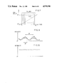
- FIG. 1 is a schematic view of an exposure apparatus embodying the present invention
- FIG. 2 is a plan view of a light amount regulating mechanism
- FIG. 3 is a chart showing the regulated light amounts obtained by the mechanism shown in FIG. 2;
- FIG. 4 is a schematic view showing the relation between a fly's eye lens and incident beams
- FIG. 5 is a view showing the relation between the oscillating direction of the beam and the cross section thereof;
- FIG. 6 is a view showing the mode of movement of light spots formed at the exit end of the fly's eye lens
- FIG. 7 is a chart showing the relation between the vibrating angle of the beam and the timing of pulse generation
- FIG. 8 is a chart showing an example of intensity distribution of interference fringes
- FIG. 9 is a chart showing an example of intensity distribution of smoothed interference fringes
- FIGS. 10A, 10B and 10C charts showing examples of the relation between the beam vibration and the timing of pulse generation
- FIG. 11 is a chart showing the mode of time-sequential pulse generation
- FIGS. 12A and 12B are flow charts showing representative function of an embodiment
- FIG. 13 is a plan view showing light source images on the pupil plane of the projection lens.
- FIG. 14 is a plan view showing the mode of beam scanning on the end face of a lens element of the optical integrator.
- the present invention will be described in detail by an embodiment thereof, applied to a stepper for projecting the pattern of a reticle onto a wafer.
- a trigger control unit 9 for generating external trigger pulses controls the oscillation of a pulsed laser unit 10 generating pulsed light beams such as an excimer laser beam.
- Said pulsed laser 10 is constructed as a stable resonator type laser having a mechanism for reducing the band width and stabilizing the wavelength, composed for example of an etalon, a dispersing element etc. positioned between two resonance mirrors positioned on both ends of a laser tube.
- the laser beam LB 0 emitted from the pulsed laser 10 is in the deep UV range, for example of a wavelength of 248 nm, and has a rectangular cross section with a vertical-to-horizontal ratio of 1/2-1/5.
- a low-speed attenuator 11 receives said beam LB 0 and reduces the light amount (energy) by 0% (complete transmission) to 100% (complete interception) in continuous level or in discrete levels.
- the attenuated beam enters a beam expander 12 composed of cylindrical lenses, and serving to emit a beam LB 1 of which cross section is transformed from the rectangular form to a substantially square form.
- a high-speed attenuator or a rapid attenuator 13 receives the beam LB 1 and attenuates the energy thereof for example in six discrete levels.
- Said high-speed attenuator 13 is for example composed of six mesh filters of different attenuating rates (transmittances) mounted on a rotary turret plate, for enabling high-speed switching of the attenuating rate during the projection of pattern of the reticle R onto the wafer W through the projection lens PL.
- FIG. 2 shows an example of said turret plate 16 and six filters 16a, 16b, 16c, 16d, 16e and 16f, in which the filter 16a consists of a simple aperture, with an attenuating rate of 0% (transmittance of 100%).
- the filters 16a-16f are positioned along a circle around the rotary shaft of the turret plate 16, with a mutual angle of about 60°, so that one of said filters is positioned in the light path of the substantially square beam LB 1 from the beam
- FIG. 3 shows the relation between the angle of rotation of the rotary turret plate 16 shown in FIG. 2 and the transmitted light amount, which is attenuated by a predetermined rate for every rotation of about 60° ( ⁇ /3).
- the transmitted light amount is 100% (attenuation of 0%) for a rotation of 2 ⁇ (360° or 0°) because the filter 16a is selected.
- the low-speed attenuator 11 and the high-speed attenuator 13 are both controlled by a light control unit 14.
- the low-speed attenuator 11 can have a slower response in comparison with the high-speed attenuator 13, but may be designed to achieve attenuation in discrete levels by means of plural mesh filters as shown in FIG. 2, or in continuous manner, in a combination of a rectangular aperture and a zoom lens system, by the change in the zooming ratio or in the aperture diameter.
- the substantially parallel beam LB 1 after desired attenuation is reflected by a vibrating mirror 20 and enters a fly's eye lens 28 serving as an optical integrator.
- Said fly's eye lens 28 is composed of a bundle of plural rod-shaped element lenses and forms secondary light source images (light spots of the beam LB 1 ) of a number corresponding to that of the element lenses.
- the vibrating mirror 20 vibrates one-dimensionally in the present embodiment, by means of an actuator employing, for example, a piezoelectric element.
- the center of vibration coincides with an imaginary line contained in the reflecting plane of the mirror 20, which therefore rotates by a small angle in reciprocating manner about said line.
- the piezoelectric element 21 is so driven by a piezo driver 22 as to obtain desired vibrating characteristics in the mirror 20. Consequently the beam LB 1 entering the fly's eye lens 28 varies its incident angle with respect to said lens 28.
- FIG. 4 is a schematic view showing the relation between the incident beam of the fly's eye lens 28 and the secondary light source images (light spots) according to the principle disclosed in the aforementioned U.S. Pat. No. 4,619,508.
- Each rod lens 28a of the fly's eye lens 28 is composed of a square quartz rod having convex spherical surfaces on both ends.
- a parallel beam LBb enters the fly's eye lens 28 parallel to the optical axis thereof, a light spot SPb is formed at the exit end of each rod lens 28a, or at a position in the air spaced by a predetermined amount from said exit end.
- FIG. 4 is a schematic view showing the relation between the incident beam of the fly's eye lens 28 and the secondary light source images (light spots) according to the principle disclosed in the aforementioned U.S. Pat. No. 4,619,508.
- Each rod lens 28a of the fly's eye lens 28 is composed of a square quartz rod having convex spherical surfaces on
- FIG. 4 shows only one light spot SPb formed on a rod lens, similar spots are formed in the exit side of all the rod lenses receiving said beam LBb, and each spot SPb is positioned at the approximate center of the exit face of the rod lens.
- a parallel beam LBa, inclined to left, with respect to the optical axis AX, in the plane of FIG. 4 is concentrated as a light spot SPa positioned at the right side of the exit plane of the rod lens 28a.
- a parallel beam LBc inclined to right with respect to the optical axis AX is concentrated as a light spot SPc positioned at the left side of the exit plane of the rod lens 28a.
- the plural beams constituting the light spots at the exit side of the fly's eye lens 28 are mostly transmitted by a beam splitter 29 as shown in FIG. 1, then enter a condenser lens 30 and are superposed on the reticle R.
- the reticle R is illuminated with a substantially uniform illumination intensity, and the photoresist layer on the wafer W is exposed, through the projection lens PL, to the pattern of the reticle R.
- the plural light spots formed at the exit end of the fly's eye lens 28 are re-formed on the entrance pupil ep of the projection lens PL, whereby a so-called Koehler illuminating system is formed.
- the wafer W is placed on a wafer stage of step-and-repeat method.
- the vibrating mirror 20 vibrates, as explained before, to displace the interference fringes (one-dimensional speckle pattern) formed on the reticle or wafer by a small amount, thereby smoothing the fringes transferred onto the photoresist layer by the integrating effect at the end of exposure, thus reducing the visibility of the interference fringes.
- the laser 10 including a stable resonator is used, the coherency of the beam in time is considerably reduced, but the spatial coherency is not sufficiently reduced, thus leaving speckles, due to the cross-sectional shape of the beam.
- FIG. 5 shows the cross section of the beams LB 0 and LB 1 .
- the beam LB 0 immediately after emerging from the laser 10 has a rectangular cross section, extended in the x-direction.
- the beam LB 0 (or LB 1 ) shows a higher spatial coherency in the y-direction perpendicular to the x-direction. Consequently, when the rod lenses 28a of the fly's eye lens 28 are arranged in the x- and y-directions as shown in FIG. 6, the interference is very weak between two light spots SP neighboring in the x-direction (longer direction of beam cross section) but is strong between two (or more) light spots SP neighboring in the y-direction (shorter direction of beam cross section).
- the beam LB 1 is vibrated by the mirror 20 in a direction F1 crossing the x-direction, as shown in FIG. 5.
- the light spots SP formed on the exit side of the rod lenses 28a of the fly's eye lens 28 simultaneously move one-dimensionally in a direction F2 as shown in FIG. 6.
- a part of the beam divided by the beam splitter 29 is concentrated on a photosensor 24 through a concentrating optical system 23.
- Said photosensor 24 is composed for example of a PIN photodiode having sufficient sensitivity in the ultraviolet wavelength range, in order to generate an exact photoelectric signal corresponding to the light amount of each pulse of the beam LB 0 (or LB 1 ).
- Said photoelectric signal is supplied to a light amount monitor circuit 26 which integrates the light amount of the pulses.
- the integrated value is supplied to a main control system 8 for exposure control
- the main control system 8 sends oscillation start and end signals to the trigger control unit 9, and instructions to the light amount control unit 14 for light amount control by the low-speed attenuator 11 or the high-speed attenuator 13.
- the main control system 8 sends a drive signal to the piezo driver 22 in order to synchronize the pulse generation of the laser 10 with the vibrating angle of the mirror 20.
- Said synchronization can also be achieved by triggering the laser 10 according to the angle of the mirror 20.
- a memory 6 is used for storing various parameters and tables required for the exposure operation and various calculations
- the half cycle of vibration of the mirror 20 corresponds to the movement of the light spot in the order of SPa - SPb - SPc (or in the reverse order), caused by an inclination of the beam by an angle ⁇ in the order of LBa - LBb - LBc (or in the reverse order)
- the actual inclination angle of the mirror 20 is equal to ⁇ /2.
- the low- and high-speed attenuators 11, 13 are composed of mesh filters of different mesh sizes, but there may be employed a rotatable polarizer if the laser beam LB 0 (or LB 1 ) is linearly polarized. In this case the transmittance of the beam can be continuously varied by the rotational position of the polarizer.
- any other structure capable of regulating the light amount or there may be employed a pulsed laser 10 equipped with means for regulating the light amount of each pulse.
- FIGS. 7 and 8 for further explaining the elimination of interference fringes on the illuminated member (reticle R or wafer W), or achieving uniform illumination intensity on said member, by the vibration of the mirror 20.
- FIG. 7 schematically shows the change in oscillation angle of the beam LB 1 entering the fly's eye lens 28, when the pulses of the laser beam LB 0 from the pulsed laser 10 have a fixed frequency (100-500 Hz), wherein the change in oscillation angle in the half cycle of the mirror 20 is assumed to be linear in time.
- 0° and ⁇ ° in the ordinate respectively correspond to the beams LBa and LBc shown in FIG. 4.
- FIG. 8 shows an example of intensity distribution in the y-direction of the interference fringes formed on the illuminated member by a pulse. It will be understood that light lines and dark lines alternate in the y-direction. However, if the fly's eye lens is composed for example of two stages, the basic component of a pitch Yp determined by the pitch of the rod lenses 28a of the fly's eye lens and the wavelength of the laser beam may be superposed with weaker interference fringes of a finer pitch.
- the reticle R In the absence of the oscillating mirror 20, the reticle R always show the interference fringes as shown in FIG. 8 at the same position, and said fringes are reproduced on the exposed pattern on the wafer W. Since the intensity of pulses of an excimer laser shows fluctuation (about ⁇ 10%), there are generally generated plural (10-100) pulses at the same position to average said fluctuation, in order to control the exposure with a desired precision. If such plural pulses contain the interference fringes as shown in FIG. 8 always at the same position of the photoresist layer on the wafer W, the uniformity of illumination is apparently insufficient for precise photolithography.
- the interference fringes as shown in FIG. 8 are displaced, on the photoresist layer, in the y-direction by a small amount ⁇ Y ( ⁇ Yp) for each of said plural pulses, whereby the interference fringes are smoothed at the end of exposure, and a substantially uniform illumination, with small ripples as shown in FIG. 9 is obtained.
- n pulses are generated during an angular change of the mirror 20 by ⁇ °/2 from the initial position as shown in FIG. 7, corresponding to the angular change of the incident beam to the fly's eye lens 28 by ⁇ ° from the initial angle (0°) or to a period from t 1 to t 2 , the change ⁇ in the oscillating angle between two pulses is approximately equal to ⁇ /n, displacing the interference fringes by an amount corresponding to ⁇ Y shown in FIG. 8.
- Pulses of a number equal to or larger than N min are generated in substantially uniform manner in the half cycle of the mirror oscillation (period of beam angular change from 0° to ⁇ °).
- Said number N min is determined by the visibility of the interference fringes (speckle) and becomes larger as the visibility increases. Said number N min is determined experimentally for example by a test exposure, and may be different between different apparatuses equipped with different optical systems. Consequently, if the pulses of a number smaller than N min are equally divided in the half cycle of beam angular change 0° to ⁇ °), there cannot be obtained uniform illumination with a desired precision.
- the average light amount of pulse at a certain angular position of the mirror should be constant for the angular range from 0° to ⁇ °.
- This condition can be satisfied by selecting the total number of pulses required for the exposure of an area (one shot) on the wafer as an integral multiple of the number Nm of the pulses during the half cycle of the beam oscillation (however Nm ⁇ N min from the foregoing condition (1)), and starting the first pulse of the exposure at the maximum angle of the mirror oscillation from 0° to ⁇ °/2 (for example at 0° providing the beam LBa shown in FIG. 4). If the total number of pulses required for the exposure of one shot is equal to an integral multiple of the number of pulses in a cycle of mirror oscillation (0°- ⁇ °/2), the first pulse in the exposure may be generated at an arbitrary angle of the mirror oscillation (0°- ⁇ °/2).
- FIGS. 10A, 10B and 10C show the angle of mirror oscillation, or the incident angle ⁇ of the beam to the fly's eye lens 28 (effectively from 0° to ⁇ °) in the ordinate as a function of time t in the abscissa, in a case of 8 pulses during the half cycle of the mirror oscillation.
- a period Te is the exposure period for a shot on the wafer, and the stepping to the next shot is conducted during the interval between the periods Te.
- Dots shown on the curve of angular change indicate the timings of pulse generation.
- FIG. 10A shows a case in which the exposure of a shot is completed in a half cycle of the mirror oscillation.
- an angular change from 0° to ⁇ ° causes the change in the incident beam from LBa to LBc shown in FIG. 4, corresponding to a displacement of the interference pattern by a pitch as shown in FIG. 8. Consequently two pulses generated at the angles 0° and ⁇ ° will cause exposures of the same interference pattern on the same position.
- the timing is so selected that a pulse is generated at 0° but not at ⁇ °, and, in case of oscillation angle change from ⁇ ° to 0°, the timing is so selected that a pulse is generated at ⁇ ° but not at 0°.
- the timing is preferably so determined that the same interference fringe pattern is not superposed at the same position.
- the number pulses in the exposure period Te is sufficiently larger than N min , for example about 100 pulses, it is scarcely necessary to consider the timing mentioned above.
- FIG. 10B shows a case in which the exposure of a shot is completed in a cycle of the mirror oscillation, so that the number of pulses per shot is doubled in comparison with the case of FIG. 10A.
- the timing of pulses is preferably so selected as to avoid overlapping in the first and second halves of the oscillation angle change (0° and ⁇ ° being also considered overlapping).
- Te half cycle of mirror oscillation
- FIG. 10C shows another case in which the oscillating mirror 20 continuously oscillates with a certain frequency, and the angular position at the first pulse in the exposure period Te is unfixed.
- the number of pulses in any exposure period Te is selected as 8 (equal to or larger than N min ) in the half cycle of the mirror oscillation, and the exposure of a shot is completed in a cycle of the mirror oscillation.
- a uniform illumination intensity and exposure control can be effectively realized at the same time, by regulating the energy of the laser beam LB and determining the optimum number of pulses so as to simultaneously satisfy the aforementioned conditions (1) and (2). Also a change in the oscillation period (speed) of the mirror 20, if combined with the change in the energy of pulse, avoids unnecessary increase in the number of pulses, and is advantageous in through-put.
- each pulse has a large energy
- a correcting exposure period containing 1 to 3 pulses of a smaller energy as shown in FIG. 11, in order to bring the integrated energy detected by the light amount monitor 26 shown in FIG. 1 exactly to a target value or an appropriate exposure value
- the energy per pulse In a pulsed laser, the energy per pulse generally fluctuates around an average value.
- the average energy per pulse (averaged value for example 100 pulses) at the exposure position (for example on the plane of projected image) is taken as P, and the amount of fluctuation thereof is taken as ⁇ P.
- the amount of appropriate energy can be represented by N ⁇ P wherein N is the average number of pulses in the coarse exposure.
- the fluctuation in the integrated energy in the correcting exposure directly influences the target appropriate energy. Consequently the maximum correcting exposure energy P' is represented by: ##EQU1## and the fluctuation ⁇ P' in each of n pulses of the correcting exposure is represented by: ##EQU2##
- ⁇ P/P is generally about 10%.
- the average number N in coarse exposure is selected larger, the fluctuation in the integrated energy at the end of coarse exposure becomes smaller, so that the number n of pulses in the correcting exposure can be reduced.
- the total number of pulses should be smaller in consideration of the throughput, so that it is desirable to reduce N by employing plural correcting pulses.
- the coarse exposure is continued with the calculation of integrated energy for each pulse with the photo-sensor 24 and the monitor 26 shown in FIG. 1, until a point where the integrated value may exceed the target value by a next pulse, in consideration of the possible fluctuation thereof.
- the discrimination level Rc for discriminating the end of coarse exposure normalized with the appropriate exposure N.P is given by (4): ##EQU5##
- the coarse exposure is continued until the measured integrated light amount, divided by N.P, exceeds said discrimination level Rc.
- the energy is preferably regulated with a maximum transmittance (100%) in the high-speed attenuator 13, and the output energy of the pulsed laser 10 or the low-speed attenuator 11 is so regulated as to obtain the optimum number N (>1) of coarse exposure pulses. In this manner the number N can be maintained low.
- the number and energy of the correcting pulses are determined from the relation (3), based on the energy thus far integrated, target value, precision A and fluctuation ⁇ P/P in the pulse energy.
- the energy is controlled by the regulation of the high-speed attenuator 13 at a desired transmittance, and the correcting exposure is conducted with the predetermined number of pulses.
- the turret plate 16 shown in FIG. 2 and having several mesh filters is suitably rotated to select a filter of desired transmittance. Since the energy transmitted in the correcting exposure is discrete as shown in FIG. 3, there will exist a suitable combination of the transmittance of the mesh filter and the number of correcting pulses for achieving the control precision A, according to the difference (deficiency in exposure) between the target value and the integrated light amount at the end of coarse exposure Also in this case it is preferable to effect confirmation according to the relation (3), assuming that the remaining correcting exposure is conducted with n pulses.
- the energy adjustment a is a ratio of the averaged pulse energy in the correcting exposure to the averaged pulse energy P in the coarse exposure.
- Values a, n satisfying: ##EQU6## will ensure a control precision ⁇ A for the integrated light amount after the correcting exposure, with respect to the appropriate exposure N.P, wherein I is the integrated light amount after the coarse exposure.
- the above-explained exposure control method can exactly control the integrated value of pulsed energy, or the total exposure to the wafer, with a desired precision.
- the present embodiment is characterized by the fact that said exposure control method is combined with the aforementioned method of obtaining uniform illumination.
- the averaged pulse energy in the coarse exposure P is larger than that in the correcting exposure, and the integrated light amount in the coarse exposure is significantly larger, naturally, than that in the correcting exposure only. Therefore it is possible to consider that uniform illumination intensity can be obtained principally from the coarse exposure
- the coarse exposure may be designed to achieve uniform illumination intensity in consideration of the number of pulses and the oscillation of the mirror 20, and uniform illumination intensity in a correcting exposure need not be particularly considered since the energy per pulse is small
- FIGS. 12A and 12B Now reference is made to flow charts shown in FIGS. 12A and 12B for explaining control sequences for executing such method.
- Said exposure S 0 can be determined for example by a test exposure and by the integrated value shown in the light amount monitor 26 when a desired integrated energy is given to the photoresist layer of the wafer. It is assumed that the coefficient K of proportionality is determined in advance between the integrated energy S given to the photoresist and the corresponding integrated value I of the monitor 26. It is also assumed that the low-speed attenuator 11 and the high-speed attenuator 13 shown in FIG. 1 are both preset at a transmittance of 100%.
- the average energy P per pulse (in mJ/cm 2 .pulse) on the exposure plane is measured with the photosensor 24 and the light amount monitor 26.
- the influence of fluctuation in the energy per pulse is canceled by the averaging of plural pulses
- the average energy P can be determined from the equation (7) with a coefficient K:
- the integrated value I on the projected image plane can also be detected, instead of the monitor 26, by a photoelectric sensor (illumination meter) placed on the X-Y stage for supporting the wafer W.
- a photoelectric sensor illumination meter
- the output thereof has to be calibrated by that of the photosensor 24.
- the photoelectric detection on the projected image plane is to be conducted in a position where the pattern (image of reticle pattern) is absent.
- the main control system 8 determines the average number N of pulses of the coarse exposure from the following equation (8), based on the measured average energy P per pulse and the appropriate exposure S 0 :
- the equation (8) means the integral part of S 0/P .
- the minimum number N min of pulses in a half cycle of the oscillating mirror 20 is experimentally determined in advance and stored in the memory 6.
- the main control system 8 reads said number N min and proceeds to the next step.
- the main control system 8 determines the minimum necessary number Nc of pulses in the coarse exposure required for securing the precision A (%) in the exposure control. Said determination may be conducted simultaneously with that of the average energy P in the step 101. Said pulse number Nc is determined from an equation (9) equivalent to (3): ##EQU7##
- the main control system 8 discriminates whether the pulse number N determined in the step 102 is larger than the minimum number Nc obtained by the equation (9) and the minimum pulse number N min in a half cycle. If at least either of Nc and N min is larger than N, the sequence proceeds to a step 105 as the desired exposure precision A or the smoothing of interference fringes cannot be attained.
- the light amount of the beam is attenuated by a predetermined proportion, for example by the low-speed attenuator 11 shown in FIG. 1. It is naturally possible also to attenuate the laser beam by the laser 10 itself.
- the main control system 8 memorizes the exact rate of attenuation A.
- the rate of attenuation is approximately determined by N/max(Nc, N min ).
- the main control system 8 discriminates whether the step 101 is to be executed again. The sequence proceeds to the step 101 or a step 107, respectively if the re-measurement is selected or not.
- the average number N of pulses in the coarse exposure is modified according to the rate of attenuation Am determined in the step 105, in the following manner:
- N' is the modified number of pulses.
- the main control system 8 determines the level Rc for discriminating the end of coarse exposure, according to the aforementioned relation (4), in which N is replaced by N' if it is newly selected in the step 107.
- this calculation is conducted by dividing the pulse number N (or N') with the integral part of the quotient obtained by dividing the average pulse number N (or N') in the coarse exposure with N min .
- the mirror 20 is set at the maximum required angular position ( ⁇ °), and the filter 16a of a transmittance 1.0 of the turret plate 16 of the high-speed attenuator 13 is aligned with the beam LB 1 to initialize the energy (100% transmission).
- the wafer W is stepped to a predetermined position (directly below the projection lens PL) by the X-Y stage, and is fixed at a position where a shot area on the wafer is aligned with the reticle R. Then the coarse exposure is initiated, and a sequence starting from a step 110 is simultaneously started.
- the oscillating mirror 20 is varied by a step ( ⁇ °), and a pulse in the coarse exposure is generated through trigger control unit 9.
- Said one-step angle ⁇ ° is determined as follows:
- the light amount monitor 26 In response to a pulse generated in the step 111, the light amount monitor 26 generates a new integrated value I, by adding a value corresponding to the light amount of a pulse to the preceding integrated value.
- the main control system 8 reads said integrated value I and determines the ratio R of the actual exposure to the appropriate exposure, according to the following equation:
- the main control system 8 compares the aforementioned discrimination level Rc with R, and the sequence proceeds to a step 113 in case of R ⁇ Rc, but returns to the step 110 in case of R ⁇ Rc.
- the coarse exposure pulses of a number Nm are given to the reticle, with a change in the beam angle by ⁇ ° each time during a half cycle of mirror oscillation, by the repetition of the above-explained steps 110-112.
- the main control system 8 discriminates whether the required control precision A is already satisfied at the end of the coarse exposure, through a comparison R ⁇ (1-A). The sequence proceeds to a next step 117 in case of R ⁇ (1-A), but to a step 114 for correcting exposure in case of R ⁇ (1-A).
- the main control system 8 determines the energy adjustment (attenuation) a and the number n of pulses required in the correcting exposure, based on the relations (5) and (6).
- a suitable mesh filter of the high-speed attenuator 13 (cf. FIG. 2) is automatically selected and set according to said energy adjustment a.
- the number of correcting pulses is generally in a range of 1 to 5, since the required adjustment a (0 ⁇ a ⁇ 1) is given by a discrete value.
- a pulse for correcting exposure is generated.
- the mirror 20 continues to be deflected by a step ( ⁇ °) in succession to the coarse exposure.
- ⁇ ° the unevenness in the illumination intensity caused by the interference fringes (one-dimensional speck pattern) on the wafer has been almost eliminated, so that the synchronization between the mirror angle and the pulse generation need not be particularly considered.
- the exposure sequence of a wafer is completed when all the shot areas on the wafer are exposed.
- control sequence according to the flow charts shown in FIGS. 12A and 12B enables the exposure operation with exposure control of a required precision and without unevenness in the illumination intensity resulting from interference fringes.
- the oscillating angle of the mirror 20 is so defined as to obtain incident beam positions to the fly's eye lens 28 which are symmetrically inclined on both sides of the optical axis AX as shown in FIG. 4, but such symmetry on both sides is not essential.
- the mirror 20 is oscillated in one-dimension only, since the interference fringes are generated principally one-dimensionally in the direction of array of the fly's eye lens 28, but, in case of two-dimensional random speckles or two-dimensional interference fringes, it becomes necessary to support the mirror 20 with a gimbal mechanism and oscillate it with piezo elements, or to employ two scanning mirrors with mutually orthogonal oscillating axes. Also in such case there can be obtained the same advantages by determining, respectively in the X- and Y-directions of beam oscillation, the minimum numbers N min (x), N min (y) of pulses required for eliminating the speckles or interference fringes in said directions, and controlling the optimum exposure based on said minimum number of pulses. It is also possible to utilize a diagonal one-dimensional oscillation of the mirror 20 having X- and Y-components therein.
- the required precision is attained by the of a correcting exposure.
- the average number N (or N') of pulses in the coarse exposure is selected sufficiently large by the use of a low-speed attenuator 11 or a high-speed attenuator 13 capable of continuously varying the rate of attenuation, or by a combination of a high-speed attenuator 11 and a low-speed attenuator 13 of discrete energy levels, the correcting exposure is scarcely necessary and may be eventually dispensed with.
- the selection of a sequence involving such correcting exposure or a sequence without such correcting exposure is made in consideration of the throughput, or the exposure time per shot.
- the total exposure time additionally includes, as shown in FIG. 11, a time required for determining and setting the energy and number of the correcting pulses, and a correcting exposure time. It is also effective, therefore, to incorporate a control sequence for calculating, in advance, the total exposure time of a mode in which the exposure is achieved by the coarse exposures only, with a reduced average energy P per pulse, and select a faster control sequence.
- FIG. 1 utilizes only one fly's eye lens 28 as the optical integrator, but there may also be employed two equivalent integrators as disclosed in the U.S. Pat. No. 4,497,015.
- Such arrangement provides secondary light source images (light spots of laser beam) of a number m 1 ⁇ m 2 on the pupil ep of the projection lens PL, wherein m 1 and m 2 are respectively numbers of rod lenses in said integrators, thereby achieving more precise uniformity of the illumination intensity.
Abstract
Description
P=I/(K·N.sub.dm) (7)
N=int(S.sub.0 /P) (8)
N'=N/Am
N.sub.m =N/int(N/N.sub.min)
Δα=α (maximum deflecting angle)/Nm
R=I/(K·S.sub.0)
Claims (5)
Applications Claiming Priority (2)
| Application Number | Priority Date | Filing Date | Title |
|---|---|---|---|
| JP63-85616 | 1988-04-07 | ||
| JP63085616A JP2569711B2 (en) | 1988-04-07 | 1988-04-07 | Exposure control device and exposure method using the same |
Publications (1)
| Publication Number | Publication Date |
|---|---|
| US4970546A true US4970546A (en) | 1990-11-13 |
Family
ID=13863778
Family Applications (1)
| Application Number | Title | Priority Date | Filing Date |
|---|---|---|---|
| US07/333,010 Expired - Lifetime US4970546A (en) | 1988-04-07 | 1989-04-04 | Exposure control device |
Country Status (2)
| Country | Link |
|---|---|
| US (1) | US4970546A (en) |
| JP (1) | JP2569711B2 (en) |
Cited By (131)
| Publication number | Priority date | Publication date | Assignee | Title |
|---|---|---|---|---|
| US5097291A (en) * | 1991-04-22 | 1992-03-17 | Nikon Corporation | Energy amount control device |
| US5119390A (en) * | 1989-08-07 | 1992-06-02 | Canon Kabushiki Kaisha | Energy amount controlling device |
| US5121160A (en) * | 1989-03-09 | 1992-06-09 | Canon Kabushiki Kaisha | Exposure method and apparatus |
| US5144362A (en) * | 1990-11-14 | 1992-09-01 | Mitsubishi Denki Kabushiki Kaisha | Projection aligner |
| US5191374A (en) * | 1988-11-17 | 1993-03-02 | Nikon Corporation | Exposure control apparatus |
| US5253040A (en) * | 1990-11-09 | 1993-10-12 | Mitsubishi Denki Kabushiki Kaisha | Projection aligner |
| US5296892A (en) * | 1992-02-01 | 1994-03-22 | Nikon Corporation | Illuminating apparatus and projection exposure apparatus provided with such an illuminating apparatus |
| US5296891A (en) * | 1990-05-02 | 1994-03-22 | Fraunhofer-Gesellschaft Zur Forderung Der Angewandten Forschung E.V. | Illumination device |
| US5300971A (en) * | 1992-02-17 | 1994-04-05 | Nikon Corporation | Projection exposure apparatus |
| US5300967A (en) * | 1992-07-31 | 1994-04-05 | Mitsubishi Denki Kabushiki Kaisha | Projection exposure apparatus |
| US5307207A (en) * | 1988-03-16 | 1994-04-26 | Nikon Corporation | Illuminating optical apparatus |
| US5400116A (en) * | 1993-11-03 | 1995-03-21 | Eastman Kodak Company | Apparatus and method for producing gradated exposures on radiation sensitive material |
| EP0655774A2 (en) * | 1993-11-02 | 1995-05-31 | Sony Corporation | Method of forming polycrystalline silicon layer and surface treatment apparatus therefor |
| US5442184A (en) * | 1993-12-10 | 1995-08-15 | Texas Instruments Incorporated | System and method for semiconductor processing using polarized radiant energy |
| US5473412A (en) * | 1993-03-08 | 1995-12-05 | Nikon Corporation | Energy amount controlling method |
| US5491534A (en) * | 1993-06-29 | 1996-02-13 | Canon Kabushiki Kaisha | Exposure apparatus and microdevice manufacturing method using the same |
| US5567928A (en) * | 1993-07-26 | 1996-10-22 | Canon Kabushiki Kaisha | Scanning exposure apparatus and method including controlling irradiation timing of an irradiation beam with respect to relative movement between the beam and a substrate |
| US5591958A (en) * | 1993-06-14 | 1997-01-07 | Nikon Corporation | Scanning exposure method and apparatus |
| US5608492A (en) * | 1994-01-26 | 1997-03-04 | Canon Kabushiki Kaisha | Scanning type exposure apparatus and method and device manufacturing method |
| US5617181A (en) * | 1994-04-28 | 1997-04-01 | Nikon Corporation | Exposure apparatus and exposure method |
| US5619376A (en) * | 1992-11-24 | 1997-04-08 | Nikon Corporation | Illuminating optical apparatus for uniformly illuminating a reticle |
| US5621529A (en) * | 1995-04-05 | 1997-04-15 | Intelligent Automation Systems, Inc. | Apparatus and method for projecting laser pattern with reduced speckle noise |
| US5627627A (en) * | 1993-02-24 | 1997-05-06 | Nikon Corporation | Exposure control apparatus and method |
| US5644383A (en) * | 1993-11-11 | 1997-07-01 | Canon Kabushiki Kaisha | Scanning exposure apparatus and device manufacturing method using the same |
| US5659383A (en) * | 1995-11-17 | 1997-08-19 | Nikon Corporation | Exposure apparatus and exposure quantity control method |
| US5673102A (en) * | 1991-02-22 | 1997-09-30 | Canon Kabushiki Kaisha | Image farming and microdevice manufacturing method and exposure apparatus in which a light source includes four quadrants of predetermined intensity |
| US5728495A (en) * | 1995-03-15 | 1998-03-17 | Nikon Corporation | Scanning exposure method and apparatus |
| US5731577A (en) * | 1995-04-21 | 1998-03-24 | Nikon Corporation | Illumination apparatus and projection exposure apparatus using the same |
| US5757838A (en) * | 1995-06-05 | 1998-05-26 | Canon Kabushiki Kaisha | Output control method for excimer laser |
| EP0844530A2 (en) * | 1996-11-25 | 1998-05-27 | Svg Lithography Systems, Inc. | Reduction of pattern noise in scanning lithographic system illuminators |
| US5798823A (en) * | 1994-11-21 | 1998-08-25 | Nikon Corporation | Illumination optical apparatus and projection exposure apparatus using it |
| US5831716A (en) * | 1993-06-10 | 1998-11-03 | Nikon Corporation | Slit-scanning type light exposure apparatus |
| US5846678A (en) * | 1994-12-22 | 1998-12-08 | Canon Kabushiki Kaisha | Exposure apparatus and device manufacturing method |
| US5854803A (en) * | 1995-01-12 | 1998-12-29 | Semiconductor Energy Laboratory Co., Ltd. | Laser illumination system |
| US5861944A (en) * | 1994-04-14 | 1999-01-19 | Nikon Corporation | Exposure apparatus |
| US5880817A (en) * | 1995-12-12 | 1999-03-09 | Nikon Corporation | Projection-exposure apparatus and method exhibiting reduced solarization and radiation compaction |
| US5892573A (en) * | 1995-09-29 | 1999-04-06 | Canon Kabushiki Kaisha | Exposure apparatus and method with multiple light receiving means |
| US5898477A (en) * | 1996-01-17 | 1999-04-27 | Canon Kabushiki Kaisha | Exposure apparatus and method of manufacturing a device using the same |
| US5912727A (en) * | 1991-12-18 | 1999-06-15 | Nikon Corporation | Projection exposure method in which mask patterns are imaged on photosensitive substrates with adjustment of illumination and projection parameters corresponding to the mask pattern |
| US5914773A (en) * | 1995-06-26 | 1999-06-22 | Canon Kabushiki Kaisha | Exposure apparatus and method using pulsed light and changing means to control both the light intensity and light emission timing |
| US5949468A (en) * | 1995-07-17 | 1999-09-07 | Canon Kabushiki Kaisha | Light quantity measuring system and exposure apparatus using the same |
| US5986744A (en) * | 1995-02-17 | 1999-11-16 | Nikon Corporation | Projection optical system, illumination apparatus, and exposure apparatus |
| US6011612A (en) * | 1992-07-03 | 2000-01-04 | Nikon Corporation | Processing apparatus using a laser light source |
| US6081319A (en) * | 1994-12-28 | 2000-06-27 | Canon Kabushiki Kaisha | Illumination system and scan type exposure apparatus |
| US6104474A (en) * | 1993-08-26 | 2000-08-15 | Nikon Corporation | Apparatus and method for controlling scanning exposure of photosensitive substrate |
| US6106139A (en) * | 1997-10-30 | 2000-08-22 | Nikon Corporation | Illumination optical apparatus and semiconductor device manufacturing method |
| EP1052545A2 (en) * | 1999-05-11 | 2000-11-15 | Carl Zeiss | Projection exposure apparatus and exposure method for microlithography |
| US6204911B1 (en) | 1995-08-30 | 2001-03-20 | Canon Kabushiki Kaisha | Exposure apparatus and device manufacturing method |
| US6252647B1 (en) * | 1990-11-15 | 2001-06-26 | Nikon Corporation | Projection exposure apparatus |
| US6252650B1 (en) | 1999-09-09 | 2001-06-26 | Nikon Corporation | Exposure apparatus, output control method for energy source, laser device using the control method, and method of producing microdevice |
| US6259510B1 (en) | 1993-02-01 | 2001-07-10 | Nikon Corporation | Exposure method and apparatus |
| US6268907B1 (en) * | 1998-05-13 | 2001-07-31 | International Business Machines Corporation | Elimination of standing waves in photoresist |
| US6268906B1 (en) * | 1993-03-15 | 2001-07-31 | Nikon Corporation | Exposure apparatus and exposure method |
| US6310679B1 (en) * | 1992-10-01 | 2001-10-30 | Nikon Corporation | Projection exposure method and apparatus |
| US6323937B1 (en) | 1998-09-28 | 2001-11-27 | Canon Kabushiki Kaisha | Projection exposure apparatus, and device manufacturing method using the same |
| EP1196947A1 (en) * | 2000-03-21 | 2002-04-17 | The Trustees Of Columbia University In The City Of New York | Surface planarization of thin silicon films during and after processing by the sequential lateral solidification method |
| EP1212784A1 (en) * | 1999-09-03 | 2002-06-12 | The Trustees Of Columbia University In The City Of New York | Methods for producing uniform large-grained and grain boundary location manipulated polycrystalline thin film semiconductors using sequential lateral solidification |
| EP1212783A1 (en) * | 1999-09-03 | 2002-06-12 | The Trustees Of Columbia University In The City Of New York | Systems and methods using sequential lateral solidification for producing single or polycrystalline silicon thin films at low temperatures |
| US6452662B2 (en) | 1998-04-08 | 2002-09-17 | Asml Netherlands B.V. | Lithography apparatus |
| US6476905B1 (en) * | 2000-01-20 | 2002-11-05 | Taiwan Semiconductor Manufacturing Co., Ltd. | Step and scan exposure system equipped with a plurality of attenuator blades for exposure control |
| US6501535B1 (en) | 1996-05-28 | 2002-12-31 | Nikon Corporation | Exposure control method and apparatus |
| US20030043356A1 (en) * | 1990-11-15 | 2003-03-06 | Nikon Corporation | Projection exposure apparatus and method |
| US6542222B1 (en) | 1999-08-02 | 2003-04-01 | Nikon Corporation | Beam output control method, beam output apparatus and exposure system, and device manufacturing method using the exposure system |
| US20030133108A1 (en) * | 2000-07-14 | 2003-07-17 | Applera Corporation | Scanning system and method for scanning a plurality of samples |
| US6636293B1 (en) | 1990-08-21 | 2003-10-21 | Nikon Corporation | Exposure method and apparatus having a decreased light intensity distribution |
| US20030196589A1 (en) * | 2002-04-17 | 2003-10-23 | Yasuhiro Mitani | Laser annealing mask and method for smoothing an annealed surface |
| US6710854B2 (en) | 1991-09-11 | 2004-03-23 | Nikon Corporation | Projection exposure apparatus |
| US20040061843A1 (en) * | 2000-11-27 | 2004-04-01 | Im James S. | Process and mask projection system for laser crystallization processing of semiconductor film regions on a substrate |
| US20040227919A1 (en) * | 1990-11-15 | 2004-11-18 | Nikon Corporation | Projection exposure apparatus and method |
| US20040233411A1 (en) * | 1990-11-15 | 2004-11-25 | Nikon Corporation | Projection exposure apparatus and method |
| US20040252386A1 (en) * | 2001-07-26 | 2004-12-16 | Fang Lei | Image transmission system from three rod lenses for rigid endoscopes |
| US20050032249A1 (en) * | 2000-03-21 | 2005-02-10 | Im James S. | Surface planarization of thin silicon films during and after processing by the sequential lateral solidification method |
| US6855486B1 (en) | 1999-09-29 | 2005-02-15 | Asml Netherlands B.V. | Lithographic method and apparatus |
| US20050034653A1 (en) * | 2001-08-27 | 2005-02-17 | James Im | Polycrystalline tft uniformity through microstructure mis-alignment |
| US20050112474A1 (en) * | 2003-11-20 | 2005-05-26 | Micronic Laser Systems Ab | Method involving a mask or a reticle |
| WO2005050720A1 (en) * | 2003-11-20 | 2005-06-02 | Micronic Laser Systems Ab | Method and apparatus for printing patterns with improved cd uniformity |
| US20050202654A1 (en) * | 2002-08-19 | 2005-09-15 | Im James S. | Process and system for laser crystallization processing of film regions on a substrate to provide substantial uniformity, and a structure of such film regions |
| US6967710B2 (en) | 1990-11-15 | 2005-11-22 | Nikon Corporation | Projection exposure apparatus and method |
| US20060006464A1 (en) * | 2002-04-01 | 2006-01-12 | Im James S | Method and system for providing a thin film with a controlled crystal orientation using pulsed laser induced melting and nucleation-initiated crystallization |
| US20060030164A1 (en) * | 2002-08-19 | 2006-02-09 | Im James S | Process and system for laser crystallization processing of film regions on a substrate to minimize edge areas, and a structure of such film regions |
| US20060055909A1 (en) * | 2004-07-29 | 2006-03-16 | Carl Zeiss Smt Ag | Illumination system for a microlithographic projection exposure apparatus |
| US20060060130A1 (en) * | 2002-08-19 | 2006-03-23 | Im James S | Process and system for laser crystallization processing of film regions on a substrate to provide substantial uniformity within arears in such regions and edge areas thereof, and a structure of film regions |
| US7046446B1 (en) * | 2004-12-15 | 2006-05-16 | Eastman Kodak Company | Speckle reduction for display system with electromechanical grating |
| US20060134890A1 (en) * | 2003-02-19 | 2006-06-22 | Im James S | System and process for processing a plurality of semiconductor thin films which are crystallized using sequential lateral solidification techniques |
| US7115503B2 (en) | 2000-10-10 | 2006-10-03 | The Trustees Of Columbia University In The City Of New York | Method and apparatus for processing thin metal layers |
| US20070007242A1 (en) * | 2003-09-16 | 2007-01-11 | The Trustees Of Columbia University In The City Of New York | Method and system for producing crystalline thin films with a uniform crystalline orientation |
| US7164152B2 (en) | 2003-09-16 | 2007-01-16 | The Trustees Of Columbia University In The City Of New York | Laser-irradiated thin films having variable thickness |
| US20070032096A1 (en) * | 2003-09-16 | 2007-02-08 | Im James S | System and process for providing multiple beam sequential lateral solidification |
| US20070117287A1 (en) * | 2005-11-23 | 2007-05-24 | Semiconductor Energy Laboratory Co., Ltd. | Laser irradiation apparatus |
| WO2007067541A2 (en) * | 2005-12-05 | 2007-06-14 | The Trustees Of Columbia University In The City Of New York | Systems and methods for processing a film, and thin films |
| US20070139660A1 (en) * | 2005-12-20 | 2007-06-21 | Semiconductor Energy Laboratory Co., Ltd. | Laser irradiation apparatus and laser irradiation method and method for manufacturing semiconductor device |
| WO2007072335A2 (en) * | 2005-12-19 | 2007-06-28 | Koninklijke Philips Electronics N.V. | Speckle reduction by angular scanning for laser projection displays |
| US20070150779A1 (en) * | 2005-12-09 | 2007-06-28 | Asml Netherlands B.V. | Lithographic apparatus and device manufacturing method |
| US7311778B2 (en) | 2003-09-19 | 2007-12-25 | The Trustees Of Columbia University In The City Of New York | Single scan irradiation for crystallization of thin films |
| US7318866B2 (en) | 2003-09-16 | 2008-01-15 | The Trustees Of Columbia University In The City Of New York | Systems and methods for inducing crystallization of thin films using multiple optical paths |
| US20080013097A1 (en) * | 2006-06-23 | 2008-01-17 | Asml Holding N.V. | Resonant scanning mirror |
| WO2008012022A1 (en) | 2006-07-24 | 2008-01-31 | Carl Zeiss Smt Ag | Optical apparatus and method for correction or improvement of the imaging behaviour of an apparatus such as this |
| US20080055579A1 (en) * | 2006-09-05 | 2008-03-06 | Joshua Monroe Cobb | Optical power modulation at high frequency |
| US7364952B2 (en) | 2003-09-16 | 2008-04-29 | The Trustees Of Columbia University In The City Of New York | Systems and methods for processing thin films |
| US20080151206A1 (en) * | 2006-12-21 | 2008-06-26 | Asml Netherlands B.V. | Lithographic apparatus and method |
| EP1975679A1 (en) | 2007-03-31 | 2008-10-01 | Sony Deutschland Gmbh | Image generating apparatus |
| US20080259450A1 (en) * | 2007-04-20 | 2008-10-23 | Canon Kabushiki Kaisha | Illumination optical apparatus, relay optical system, exposure apparatus, and device manufacturing method |
| US20090135398A1 (en) * | 2007-11-22 | 2009-05-28 | Canon Kabushiki Kaisha | Exposure apparatus and device manufacturing method |
| US7638728B2 (en) | 2003-09-16 | 2009-12-29 | The Trustees Of Columbia University In The City Of New York | Enhancing the width of polycrystalline grains with mask |
| US7645337B2 (en) | 2004-11-18 | 2010-01-12 | The Trustees Of Columbia University In The City Of New York | Systems and methods for creating crystallographic-orientation controlled poly-silicon films |
| US7656504B1 (en) * | 1990-08-21 | 2010-02-02 | Nikon Corporation | Projection exposure apparatus with luminous flux distribution |
| US7718517B2 (en) | 2002-08-19 | 2010-05-18 | Im James S | Single-shot semiconductor processing system and method having various irradiation patterns |
| US7759230B2 (en) | 2003-09-16 | 2010-07-20 | The Trustees Of Columbia University In The City Of New York | System for providing a continuous motion sequential lateral solidification for reducing or eliminating artifacts in overlap regions, and a mask for facilitating such artifact reduction/elimination |
| DE102009037113A1 (en) * | 2009-07-31 | 2010-09-23 | Carl Zeiss Laser Optics Gmbh | Suppressing interference effects on surface illuminated by laser beam, comprises guiding laser beam through optical elements before impinging on surface, and oscillatingly changing one of the optical elements in their optical properties |
| US20110095006A1 (en) * | 2009-10-26 | 2011-04-28 | Toshiba Kikai Kabushiki Kaisha | Laser dicing method and laser dicing apparatus |
| US8012861B2 (en) | 2007-11-21 | 2011-09-06 | The Trustees Of Columbia University In The City Of New York | Systems and methods for preparing epitaxially textured polycrystalline films |
| US8221544B2 (en) | 2005-04-06 | 2012-07-17 | The Trustees Of Columbia University In The City Of New York | Line scan sequential lateral solidification of thin films |
| US8415670B2 (en) | 2007-09-25 | 2013-04-09 | The Trustees Of Columbia University In The City Of New York | Methods of producing high uniformity in thin film transistor devices fabricated on laterally crystallized thin films |
| US8426296B2 (en) | 2007-11-21 | 2013-04-23 | The Trustees Of Columbia University In The City Of New York | Systems and methods for preparing epitaxially textured polycrystalline films |
| US8440581B2 (en) | 2009-11-24 | 2013-05-14 | The Trustees Of Columbia University In The City Of New York | Systems and methods for non-periodic pulse sequential lateral solidification |
| CN103336410A (en) * | 2013-06-27 | 2013-10-02 | 上海华力微电子有限公司 | Device for enhancing capability of lithographic process and lithographic process using same |
| US8557040B2 (en) | 2007-11-21 | 2013-10-15 | The Trustees Of Columbia University In The City Of New York | Systems and methods for preparation of epitaxially textured thick films |
| US8569155B2 (en) | 2008-02-29 | 2013-10-29 | The Trustees Of Columbia University In The City Of New York | Flash lamp annealing crystallization for large area thin films |
| US8614471B2 (en) | 2007-09-21 | 2013-12-24 | The Trustees Of Columbia University In The City Of New York | Collections of laterally crystallized semiconductor islands for use in thin film transistors |
| US8663387B2 (en) | 2003-09-16 | 2014-03-04 | The Trustees Of Columbia University In The City Of New York | Method and system for facilitating bi-directional growth |
| US8796159B2 (en) | 2003-09-16 | 2014-08-05 | The Trustees Of Columbia University In The City Of New York | Processes and systems for laser crystallization processing of film regions on a substrate utilizing a line-type beam, and structures of such film regions |
| US8802580B2 (en) | 2008-11-14 | 2014-08-12 | The Trustees Of Columbia University In The City Of New York | Systems and methods for the crystallization of thin films |
| US8871540B2 (en) | 2011-07-27 | 2014-10-28 | Toshiba Kikai Kabushiki Kaisha | Laser dicing method |
| US8895345B2 (en) | 2010-06-24 | 2014-11-25 | Toshiba Kikai Kabushiki Kaisha | Dicing methods |
| US9087696B2 (en) | 2009-11-03 | 2015-07-21 | The Trustees Of Columbia University In The City Of New York | Systems and methods for non-periodic pulse partial melt film processing |
| USRE46092E1 (en) | 2007-11-20 | 2016-08-02 | Daniel Redlich | Revenue sharing system that incentivizes content providers and registered users and includes payment processing |
| TWI577488B (en) * | 2014-11-17 | 2017-04-11 | 財團法人工業技術研究院 | Surface processing method |
| US9646831B2 (en) | 2009-11-03 | 2017-05-09 | The Trustees Of Columbia University In The City Of New York | Advanced excimer laser annealing for thin films |
| US10016843B2 (en) | 2015-03-20 | 2018-07-10 | Ultratech, Inc. | Systems and methods for reducing pulsed laser beam profile non-uniformities for laser annealing |
| US20190346774A1 (en) * | 2018-05-08 | 2019-11-14 | Canon Kabushiki Kaisha | Measurement apparatus, exposure apparatus, and method of manufacturing article |
| US10620447B2 (en) | 2017-01-19 | 2020-04-14 | Cognex Corporation | System and method for reduced-speckle laser line generation |
Families Citing this family (2)
| Publication number | Priority date | Publication date | Assignee | Title |
|---|---|---|---|---|
| JP3200894B2 (en) | 1991-03-05 | 2001-08-20 | 株式会社日立製作所 | Exposure method and apparatus |
| JP5178047B2 (en) * | 2007-05-01 | 2013-04-10 | ギガフォトン株式会社 | Discharge excitation laser equipment for exposure |
Citations (5)
| Publication number | Priority date | Publication date | Assignee | Title |
|---|---|---|---|---|
| US4497015A (en) * | 1982-02-26 | 1985-01-29 | Nippon Kogaku K.K. | Light illumination device |
| JPS60169136A (en) * | 1984-02-14 | 1985-09-02 | Canon Inc | Exposure controlling method and unit therefor |
| US4619508A (en) * | 1984-04-28 | 1986-10-28 | Nippon Kogaku K. K. | Illumination optical arrangement |
| US4653903A (en) * | 1984-01-24 | 1987-03-31 | Canon Kabushiki Kaisha | Exposure apparatus |
| JPS6381882A (en) * | 1986-09-25 | 1988-04-12 | Nikon Corp | Energy controller |
Family Cites Families (4)
| Publication number | Priority date | Publication date | Assignee | Title |
|---|---|---|---|---|
| FR2406236A1 (en) * | 1976-12-10 | 1979-05-11 | Thomson Csf | OPTICAL DEVICE WITH COHERENT SOURCE FOR THE QUICK TRANSFER OF PATTERNS ON SUBSTRATES, APPLIED TO THE REALIZATION OF COMPONENTS AND MICROSTRUCTURE CIRCUITS |
| JPS59226317A (en) * | 1983-06-06 | 1984-12-19 | Nippon Kogaku Kk <Nikon> | Illuminating device |
| JPH0715875B2 (en) * | 1984-12-27 | 1995-02-22 | キヤノン株式会社 | Exposure apparatus and method |
| JPS61212816A (en) * | 1985-03-18 | 1986-09-20 | Canon Inc | Lighting equipment |
-
1988
- 1988-04-07 JP JP63085616A patent/JP2569711B2/en not_active Expired - Lifetime
-
1989
- 1989-04-04 US US07/333,010 patent/US4970546A/en not_active Expired - Lifetime
Patent Citations (5)
| Publication number | Priority date | Publication date | Assignee | Title |
|---|---|---|---|---|
| US4497015A (en) * | 1982-02-26 | 1985-01-29 | Nippon Kogaku K.K. | Light illumination device |
| US4653903A (en) * | 1984-01-24 | 1987-03-31 | Canon Kabushiki Kaisha | Exposure apparatus |
| JPS60169136A (en) * | 1984-02-14 | 1985-09-02 | Canon Inc | Exposure controlling method and unit therefor |
| US4619508A (en) * | 1984-04-28 | 1986-10-28 | Nippon Kogaku K. K. | Illumination optical arrangement |
| JPS6381882A (en) * | 1986-09-25 | 1988-04-12 | Nikon Corp | Energy controller |
Cited By (244)
| Publication number | Priority date | Publication date | Assignee | Title |
|---|---|---|---|---|
| US5307207A (en) * | 1988-03-16 | 1994-04-26 | Nikon Corporation | Illuminating optical apparatus |
| US5191374A (en) * | 1988-11-17 | 1993-03-02 | Nikon Corporation | Exposure control apparatus |
| US5121160A (en) * | 1989-03-09 | 1992-06-09 | Canon Kabushiki Kaisha | Exposure method and apparatus |
| US5119390A (en) * | 1989-08-07 | 1992-06-02 | Canon Kabushiki Kaisha | Energy amount controlling device |
| US5296891A (en) * | 1990-05-02 | 1994-03-22 | Fraunhofer-Gesellschaft Zur Forderung Der Angewandten Forschung E.V. | Illumination device |
| US7656504B1 (en) * | 1990-08-21 | 2010-02-02 | Nikon Corporation | Projection exposure apparatus with luminous flux distribution |
| US6636293B1 (en) | 1990-08-21 | 2003-10-21 | Nikon Corporation | Exposure method and apparatus having a decreased light intensity distribution |
| US5253040A (en) * | 1990-11-09 | 1993-10-12 | Mitsubishi Denki Kabushiki Kaisha | Projection aligner |
| US5144362A (en) * | 1990-11-14 | 1992-09-01 | Mitsubishi Denki Kabushiki Kaisha | Projection aligner |
| US6710855B2 (en) | 1990-11-15 | 2004-03-23 | Nikon Corporation | Projection exposure apparatus and method |
| US6897942B2 (en) | 1990-11-15 | 2005-05-24 | Nikon Corporation | Projection exposure apparatus and method |
| US20030043356A1 (en) * | 1990-11-15 | 2003-03-06 | Nikon Corporation | Projection exposure apparatus and method |
| US20040227919A1 (en) * | 1990-11-15 | 2004-11-18 | Nikon Corporation | Projection exposure apparatus and method |
| US6967710B2 (en) | 1990-11-15 | 2005-11-22 | Nikon Corporation | Projection exposure apparatus and method |
| US6252647B1 (en) * | 1990-11-15 | 2001-06-26 | Nikon Corporation | Projection exposure apparatus |
| US20040233411A1 (en) * | 1990-11-15 | 2004-11-25 | Nikon Corporation | Projection exposure apparatus and method |
| US6665050B2 (en) | 1990-11-15 | 2003-12-16 | Nikon Corporation | Projection exposure methods using difracted light with increased intensity portions spaced from the optical axis |
| US6704092B2 (en) | 1990-11-15 | 2004-03-09 | Nikon Corporation | Projection exposure method and apparatus that produces an intensity distribution on a plane substantially conjugate to a projection optical system pupil plane |
| US6885433B2 (en) | 1990-11-15 | 2005-04-26 | Nikon Corporation | Projection exposure apparatus and method |
| US5673102A (en) * | 1991-02-22 | 1997-09-30 | Canon Kabushiki Kaisha | Image farming and microdevice manufacturing method and exposure apparatus in which a light source includes four quadrants of predetermined intensity |
| US6128068A (en) * | 1991-02-22 | 2000-10-03 | Canon Kabushiki Kaisha | Projection exposure apparatus including an illumination optical system that forms a secondary light source with a particular intensity distribution |
| US6084655A (en) * | 1991-02-22 | 2000-07-04 | Canon Kabushiki Kaisha | Imaging method for manufacture of microdevices |
| US5097291A (en) * | 1991-04-22 | 1992-03-17 | Nikon Corporation | Energy amount control device |
| US6864959B2 (en) | 1991-09-11 | 2005-03-08 | Nikon Corporation | Projection exposure apparatus |
| US6710854B2 (en) | 1991-09-11 | 2004-03-23 | Nikon Corporation | Projection exposure apparatus |
| US5912727A (en) * | 1991-12-18 | 1999-06-15 | Nikon Corporation | Projection exposure method in which mask patterns are imaged on photosensitive substrates with adjustment of illumination and projection parameters corresponding to the mask pattern |
| US6175405B1 (en) * | 1991-12-18 | 2001-01-16 | Nikon Corporation | Projection exposure method and method of manufacturing a projection exposure apparatus |
| US5296892A (en) * | 1992-02-01 | 1994-03-22 | Nikon Corporation | Illuminating apparatus and projection exposure apparatus provided with such an illuminating apparatus |
| US5300971A (en) * | 1992-02-17 | 1994-04-05 | Nikon Corporation | Projection exposure apparatus |
| US6011612A (en) * | 1992-07-03 | 2000-01-04 | Nikon Corporation | Processing apparatus using a laser light source |
| US5300967A (en) * | 1992-07-31 | 1994-04-05 | Mitsubishi Denki Kabushiki Kaisha | Projection exposure apparatus |
| US6310679B1 (en) * | 1992-10-01 | 2001-10-30 | Nikon Corporation | Projection exposure method and apparatus |
| US5619376A (en) * | 1992-11-24 | 1997-04-08 | Nikon Corporation | Illuminating optical apparatus for uniformly illuminating a reticle |
| US5745294A (en) * | 1992-11-24 | 1998-04-28 | Nikon Corporation | Illuminating optical apparatus |
| US6259510B1 (en) | 1993-02-01 | 2001-07-10 | Nikon Corporation | Exposure method and apparatus |
| US6411364B1 (en) | 1993-02-01 | 2002-06-25 | Nikon Corporation | Exposure apparatus |
| US5627627A (en) * | 1993-02-24 | 1997-05-06 | Nikon Corporation | Exposure control apparatus and method |
| US6456363B2 (en) * | 1993-02-24 | 2002-09-24 | Nikon Corporation | Exposure control apparatus and method |
| US6222615B1 (en) * | 1993-02-24 | 2001-04-24 | Nikon Corporation | Exposure control apparatus and method |
| US5473412A (en) * | 1993-03-08 | 1995-12-05 | Nikon Corporation | Energy amount controlling method |
| US6496247B2 (en) | 1993-03-15 | 2002-12-17 | Nikon Corporation | Exposure apparatus and exposure method |
| US6268906B1 (en) * | 1993-03-15 | 2001-07-31 | Nikon Corporation | Exposure apparatus and exposure method |
| US6713747B2 (en) | 1993-06-10 | 2004-03-30 | Nikon Corporation | Light exposure apparatus |
| US5831716A (en) * | 1993-06-10 | 1998-11-03 | Nikon Corporation | Slit-scanning type light exposure apparatus |
| US6100515A (en) * | 1993-06-14 | 2000-08-08 | Nikon Corporation | Scanning exposure method and apparatus in which a mask and a substrate are moved at different scan velocities and exposure parameters are varied |
| US5591958A (en) * | 1993-06-14 | 1997-01-07 | Nikon Corporation | Scanning exposure method and apparatus |
| US6396071B1 (en) | 1993-06-14 | 2002-05-28 | Nikon Corporation | Scanning exposure method and apparatus |
| US5699148A (en) * | 1993-06-29 | 1997-12-16 | Canon Kabushiki Kaisha | Exposure apparatus and microdevice manufacturing method using the same |
| US5491534A (en) * | 1993-06-29 | 1996-02-13 | Canon Kabushiki Kaisha | Exposure apparatus and microdevice manufacturing method using the same |
| US5567928A (en) * | 1993-07-26 | 1996-10-22 | Canon Kabushiki Kaisha | Scanning exposure apparatus and method including controlling irradiation timing of an irradiation beam with respect to relative movement between the beam and a substrate |
| US6104474A (en) * | 1993-08-26 | 2000-08-15 | Nikon Corporation | Apparatus and method for controlling scanning exposure of photosensitive substrate |
| EP1179381A3 (en) * | 1993-11-02 | 2002-02-20 | Sony Corporation | Surface treatment apparatus |
| EP0655774A3 (en) * | 1993-11-02 | 1996-07-17 | Sony Corp | Method of forming polycrystalline silicon layer and surface treatment apparatus therefor. |
| EP0655774A2 (en) * | 1993-11-02 | 1995-05-31 | Sony Corporation | Method of forming polycrystalline silicon layer and surface treatment apparatus therefor |
| KR100299292B1 (en) * | 1993-11-02 | 2001-12-01 | 이데이 노부유끼 | Polysilicon Thin Film Forming Method and Surface Treatment Apparatus |
| EP1179381A2 (en) * | 1993-11-02 | 2002-02-13 | Sony Corporation | Surface treatment apparatus |
| US5869803A (en) * | 1993-11-02 | 1999-02-09 | Sony Corporation | Method of forming polycrystalline silicon layer on substrate and surface treatment apparatus thereof |
| US5400116A (en) * | 1993-11-03 | 1995-03-21 | Eastman Kodak Company | Apparatus and method for producing gradated exposures on radiation sensitive material |
| US5644383A (en) * | 1993-11-11 | 1997-07-01 | Canon Kabushiki Kaisha | Scanning exposure apparatus and device manufacturing method using the same |
| US5442184A (en) * | 1993-12-10 | 1995-08-15 | Texas Instruments Incorporated | System and method for semiconductor processing using polarized radiant energy |
| US5608492A (en) * | 1994-01-26 | 1997-03-04 | Canon Kabushiki Kaisha | Scanning type exposure apparatus and method and device manufacturing method |
| US5861944A (en) * | 1994-04-14 | 1999-01-19 | Nikon Corporation | Exposure apparatus |
| US5617181A (en) * | 1994-04-28 | 1997-04-01 | Nikon Corporation | Exposure apparatus and exposure method |
| US5798823A (en) * | 1994-11-21 | 1998-08-25 | Nikon Corporation | Illumination optical apparatus and projection exposure apparatus using it |
| US5846678A (en) * | 1994-12-22 | 1998-12-08 | Canon Kabushiki Kaisha | Exposure apparatus and device manufacturing method |
| US6081319A (en) * | 1994-12-28 | 2000-06-27 | Canon Kabushiki Kaisha | Illumination system and scan type exposure apparatus |
| US5854803A (en) * | 1995-01-12 | 1998-12-29 | Semiconductor Energy Laboratory Co., Ltd. | Laser illumination system |
| US20050023255A1 (en) * | 1995-01-13 | 2005-02-03 | Semiconductor Energy Laboratory Co., Ltd. | Laser illumination system |
| US6468842B2 (en) | 1995-01-13 | 2002-10-22 | Semiconductor Energy Laboratory Co., Ltd. | Laser illumination system |
| US6784030B2 (en) | 1995-01-13 | 2004-08-31 | Semiconductor Energy Laboratory Co., Ltd. | Laser illumination system |
| US6210996B1 (en) | 1995-01-13 | 2001-04-03 | Semiconductor Energy Laboratory Co., Ltd. | Laser illumination system |
| US7528079B2 (en) | 1995-01-13 | 2009-05-05 | Semiconductor Energy Laboratory Co., Ltd. | Method of changing an energy attenuation factor of a linear light in order to crystallize a semiconductor film |
| US6706570B2 (en) | 1995-01-13 | 2004-03-16 | Semiconductor Energy Laboratory Co., Ltd., | Laser illumination system |
| US5986744A (en) * | 1995-02-17 | 1999-11-16 | Nikon Corporation | Projection optical system, illumination apparatus, and exposure apparatus |
| US6154270A (en) * | 1995-03-15 | 2000-11-28 | Nikon Corporation | Scanning exposure method and apparatus |
| US5728495A (en) * | 1995-03-15 | 1998-03-17 | Nikon Corporation | Scanning exposure method and apparatus |
| US5621529A (en) * | 1995-04-05 | 1997-04-15 | Intelligent Automation Systems, Inc. | Apparatus and method for projecting laser pattern with reduced speckle noise |
| US5731577A (en) * | 1995-04-21 | 1998-03-24 | Nikon Corporation | Illumination apparatus and projection exposure apparatus using the same |
| US5757838A (en) * | 1995-06-05 | 1998-05-26 | Canon Kabushiki Kaisha | Output control method for excimer laser |
| US5914773A (en) * | 1995-06-26 | 1999-06-22 | Canon Kabushiki Kaisha | Exposure apparatus and method using pulsed light and changing means to control both the light intensity and light emission timing |
| US5949468A (en) * | 1995-07-17 | 1999-09-07 | Canon Kabushiki Kaisha | Light quantity measuring system and exposure apparatus using the same |
| US6424405B2 (en) | 1995-08-30 | 2002-07-23 | Canon Kabushiki Kaisha | Exposure apparatus and device manufacturing method |
| US6204911B1 (en) | 1995-08-30 | 2001-03-20 | Canon Kabushiki Kaisha | Exposure apparatus and device manufacturing method |
| US5892573A (en) * | 1995-09-29 | 1999-04-06 | Canon Kabushiki Kaisha | Exposure apparatus and method with multiple light receiving means |
| US5659383A (en) * | 1995-11-17 | 1997-08-19 | Nikon Corporation | Exposure apparatus and exposure quantity control method |
| US5929977A (en) * | 1995-11-17 | 1999-07-27 | Nikon Corporation | Exposure apparatus and exposure quantity control method |
| US5880817A (en) * | 1995-12-12 | 1999-03-09 | Nikon Corporation | Projection-exposure apparatus and method exhibiting reduced solarization and radiation compaction |
| US5898477A (en) * | 1996-01-17 | 1999-04-27 | Canon Kabushiki Kaisha | Exposure apparatus and method of manufacturing a device using the same |
| US6501535B1 (en) | 1996-05-28 | 2002-12-31 | Nikon Corporation | Exposure control method and apparatus |
| US8680427B2 (en) | 1996-05-28 | 2014-03-25 | The Trustees Of Columbia University In The City Of New York | Uniform large-grained and gain boundary location manipulated polycrystalline thin film semiconductors formed using sequential lateral solidification and devices formed thereon |
| US8278659B2 (en) | 1996-05-28 | 2012-10-02 | The Trustees Of Columbia University In The City Of New York | Uniform large-grained and grain boundary location manipulated polycrystalline thin film semiconductors formed using sequential lateral solidification and devices formed thereon |
| US8859436B2 (en) | 1996-05-28 | 2014-10-14 | The Trustees Of Columbia University In The City Of New York | Uniform large-grained and grain boundary location manipulated polycrystalline thin film semiconductors formed using sequential lateral solidification and devices formed thereon |
| US20050255640A1 (en) * | 1996-05-28 | 2005-11-17 | Im James S | Methods for producing uniform large-grained and grain boundary location manipulated polycrystalline thin film semiconductors using sequential lateral solidification |
| US7679028B2 (en) | 1996-05-28 | 2010-03-16 | The Trustees Of Columbia University In The City Of New York | Methods for producing uniform large-grained and grain boundary location manipulated polycrystalline thin film semiconductors using sequential lateral solidification |
| US7319056B2 (en) | 1996-05-28 | 2008-01-15 | The Trustees Of Columbia University In The City Of New York | Methods for producing uniform large-grained and grain boundary location manipulated polycrystalline thin film semiconductors using sequential lateral solidification |
| EP0844530A3 (en) * | 1996-11-25 | 2000-05-03 | Svg Lithography Systems, Inc. | Reduction of pattern noise in scanning lithographic system illuminators |
| EP0844530A2 (en) * | 1996-11-25 | 1998-05-27 | Svg Lithography Systems, Inc. | Reduction of pattern noise in scanning lithographic system illuminators |
| US6106139A (en) * | 1997-10-30 | 2000-08-22 | Nikon Corporation | Illumination optical apparatus and semiconductor device manufacturing method |
| US6452662B2 (en) | 1998-04-08 | 2002-09-17 | Asml Netherlands B.V. | Lithography apparatus |
| US20040051858A1 (en) * | 1998-04-08 | 2004-03-18 | Asml Netherlands B.V. | Lithography apparatus |
| US7061583B2 (en) | 1998-04-08 | 2006-06-13 | Asml Netherlands B.V. | Lithography apparatus |
| US6268907B1 (en) * | 1998-05-13 | 2001-07-31 | International Business Machines Corporation | Elimination of standing waves in photoresist |
| US6323937B1 (en) | 1998-09-28 | 2001-11-27 | Canon Kabushiki Kaisha | Projection exposure apparatus, and device manufacturing method using the same |
| US6577381B2 (en) | 1998-09-28 | 2003-06-10 | Canon Kabushiki Kaisha | Projection exposure apparatus, and device manufacturing method using the same |
| EP1052545A2 (en) * | 1999-05-11 | 2000-11-15 | Carl Zeiss | Projection exposure apparatus and exposure method for microlithography |
| EP1052545A3 (en) * | 1999-05-11 | 2004-01-21 | Carl Zeiss | Projection exposure apparatus and exposure method for microlithography |
| US6542222B1 (en) | 1999-08-02 | 2003-04-01 | Nikon Corporation | Beam output control method, beam output apparatus and exposure system, and device manufacturing method using the exposure system |
| EP1212784A1 (en) * | 1999-09-03 | 2002-06-12 | The Trustees Of Columbia University In The City Of New York | Methods for producing uniform large-grained and grain boundary location manipulated polycrystalline thin film semiconductors using sequential lateral solidification |
| EP1212783A4 (en) * | 1999-09-03 | 2003-02-05 | Univ Columbia | Systems and methods using sequential lateral solidification for producing single or polycrystalline silicon thin films at low temperatures |
| EP1816673A3 (en) * | 1999-09-03 | 2007-11-14 | The Trustees of Columbia University in the City of New York | Methods for producing uniform large-grained and grain boundary location manipulated polycrystalline thin film semiconductors using sequential lateral solidification |
| EP1914793A1 (en) * | 1999-09-03 | 2008-04-23 | The Trustees of Columbia University | Systems and methods using sequential lateral solidification for producing single or polycrystalline silicon thin films at low temperatures |
| EP1816673A2 (en) | 1999-09-03 | 2007-08-08 | The Trustees of Columbia University of the City of New York | Methods for producing uniform large-grained and grain boundary location manipulated polycrystalline thin film semiconductors using sequential lateral solidification |
| EP1212783A1 (en) * | 1999-09-03 | 2002-06-12 | The Trustees Of Columbia University In The City Of New York | Systems and methods using sequential lateral solidification for producing single or polycrystalline silicon thin films at low temperatures |
| US6573531B1 (en) | 1999-09-03 | 2003-06-03 | The Trustees Of Columbia University In The City Of New York | Systems and methods using sequential lateral solidification for producing single or polycrystalline silicon thin films at low temperatures |
| US7029996B2 (en) | 1999-09-03 | 2006-04-18 | The Trustees Of Columbia University In The City Of New York | Methods for producing uniform large-grained and grain boundary location manipulated polycrystalline thin film semiconductors using sequential lateral solidification |
| EP1212784A4 (en) * | 1999-09-03 | 2003-01-29 | Univ Columbia | Methods for producing uniform large-grained and grain boundary location manipulated polycrystalline thin film semiconductors using sequential lateral solidification |
| US20030096489A1 (en) * | 1999-09-03 | 2003-05-22 | Im James S. | Methods for producing uniform large-grained and grain boundary location manipulated polycrystalline thin film semiconductors using sequential lateral solidification |
| US6252650B1 (en) | 1999-09-09 | 2001-06-26 | Nikon Corporation | Exposure apparatus, output control method for energy source, laser device using the control method, and method of producing microdevice |
| US6855486B1 (en) | 1999-09-29 | 2005-02-15 | Asml Netherlands B.V. | Lithographic method and apparatus |
| US6476905B1 (en) * | 2000-01-20 | 2002-11-05 | Taiwan Semiconductor Manufacturing Co., Ltd. | Step and scan exposure system equipped with a plurality of attenuator blades for exposure control |
| US7704862B2 (en) | 2000-03-21 | 2010-04-27 | The Trustees Of Columbia University | Surface planarization of thin silicon films during and after processing by the sequential lateral solidification method |
| US20050032249A1 (en) * | 2000-03-21 | 2005-02-10 | Im James S. | Surface planarization of thin silicon films during and after processing by the sequential lateral solidification method |
| US7220660B2 (en) | 2000-03-21 | 2007-05-22 | The Trustees Of Columbia University In The City Of New York | Surface planarization of thin silicon films during and after processing by the sequential lateral solidification method |
| EP1196947A4 (en) * | 2000-03-21 | 2003-08-13 | Univ Columbia | Surface planarization of thin silicon films during and after processing by the sequential lateral solidification method |
| EP1196947A1 (en) * | 2000-03-21 | 2002-04-17 | The Trustees Of Columbia University In The City Of New York | Surface planarization of thin silicon films during and after processing by the sequential lateral solidification method |
| US6965105B2 (en) * | 2000-07-14 | 2005-11-15 | Applera Corporation | Scanning system and method for scanning a plurality of samples |
| US20030133108A1 (en) * | 2000-07-14 | 2003-07-17 | Applera Corporation | Scanning system and method for scanning a plurality of samples |
| US20090140173A1 (en) * | 2000-10-10 | 2009-06-04 | Im James S | Method and apparatus for processing thin metal layers |
| US7709378B2 (en) | 2000-10-10 | 2010-05-04 | The Trustees Of Columbia University In The City Of New York | Method and apparatus for processing thin metal layers |
| US7115503B2 (en) | 2000-10-10 | 2006-10-03 | The Trustees Of Columbia University In The City Of New York | Method and apparatus for processing thin metal layers |
| US6961117B2 (en) | 2000-11-27 | 2005-11-01 | The Trustees Of Columbia University In The City Of New York | Process and mask projection system for laser crystallization processing of semiconductor film regions on a substrate |
| US20040061843A1 (en) * | 2000-11-27 | 2004-04-01 | Im James S. | Process and mask projection system for laser crystallization processing of semiconductor film regions on a substrate |
| US7586679B2 (en) * | 2001-07-26 | 2009-09-08 | Karl Storz Gmbh & Co. Kg | Image transmission system from three rod lenses for rigid endoscopes |
| US20040252386A1 (en) * | 2001-07-26 | 2004-12-16 | Fang Lei | Image transmission system from three rod lenses for rigid endoscopes |
| US7160763B2 (en) | 2001-08-27 | 2007-01-09 | The Trustees Of Columbia University In The City Of New York | Polycrystalline TFT uniformity through microstructure mis-alignment |
| US20050034653A1 (en) * | 2001-08-27 | 2005-02-17 | James Im | Polycrystalline tft uniformity through microstructure mis-alignment |
| US20060006464A1 (en) * | 2002-04-01 | 2006-01-12 | Im James S | Method and system for providing a thin film with a controlled crystal orientation using pulsed laser induced melting and nucleation-initiated crystallization |
| US7399359B2 (en) | 2002-04-01 | 2008-07-15 | The Trustees of Columbia University in theCity of New York | Method and system for providing a thin film with a controlled crystal orientation using pulsed laser induced melting and nucleation-initiated crystallization |
| US20030196589A1 (en) * | 2002-04-17 | 2003-10-23 | Yasuhiro Mitani | Laser annealing mask and method for smoothing an annealed surface |
| US7192479B2 (en) * | 2002-04-17 | 2007-03-20 | Sharp Laboratories Of America, Inc. | Laser annealing mask and method for smoothing an annealed surface |
| US20060030164A1 (en) * | 2002-08-19 | 2006-02-09 | Im James S | Process and system for laser crystallization processing of film regions on a substrate to minimize edge areas, and a structure of such film regions |
| US20050202654A1 (en) * | 2002-08-19 | 2005-09-15 | Im James S. | Process and system for laser crystallization processing of film regions on a substrate to provide substantial uniformity, and a structure of such film regions |
| US7622370B2 (en) | 2002-08-19 | 2009-11-24 | The Trustees Of Columbia University In The City Of New York | Process and system for laser crystallization processing of film regions on a substrate to minimize edge areas, and a structure of such film regions |
| US8883656B2 (en) | 2002-08-19 | 2014-11-11 | The Trustees Of Columbia University In The City Of New York | Single-shot semiconductor processing system and method having various irradiation patterns |
| US7718517B2 (en) | 2002-08-19 | 2010-05-18 | Im James S | Single-shot semiconductor processing system and method having various irradiation patterns |
| US8479681B2 (en) | 2002-08-19 | 2013-07-09 | The Trustees Of Columbia University In The City Of New York | Single-shot semiconductor processing system and method having various irradiation patterns |
| US7259081B2 (en) | 2002-08-19 | 2007-08-21 | Im James S | Process and system for laser crystallization processing of film regions on a substrate to provide substantial uniformity, and a structure of such film regions |
| US8411713B2 (en) | 2002-08-19 | 2013-04-02 | The Trustees Of Columbia University In The City Of New York | Process and system for laser crystallization processing of film regions on a substrate to minimize edge areas, and structure of such film regions |
| US20060060130A1 (en) * | 2002-08-19 | 2006-03-23 | Im James S | Process and system for laser crystallization processing of film regions on a substrate to provide substantial uniformity within arears in such regions and edge areas thereof, and a structure of film regions |
| US7906414B2 (en) | 2002-08-19 | 2011-03-15 | The Trustees Of Columbia University In The City Of New York | Single-shot semiconductor processing system and method having various irradiation patterns |
| US7300858B2 (en) | 2002-08-19 | 2007-11-27 | The Trustees Of Columbia University In The City Of New York | Laser crystallization and selective patterning using multiple beamlets |
| US20060134890A1 (en) * | 2003-02-19 | 2006-06-22 | Im James S | System and process for processing a plurality of semiconductor thin films which are crystallized using sequential lateral solidification techniques |
| US7902052B2 (en) | 2003-02-19 | 2011-03-08 | The Trustees Of Columbia University In The City Of New York | System and process for processing a plurality of semiconductor thin films which are crystallized using sequential lateral solidification techniques |
| US7341928B2 (en) | 2003-02-19 | 2008-03-11 | The Trustees Of Columbia University In The City Of New York | System and process for processing a plurality of semiconductor thin films which are crystallized using sequential lateral solidification techniques |
| US8663387B2 (en) | 2003-09-16 | 2014-03-04 | The Trustees Of Columbia University In The City Of New York | Method and system for facilitating bi-directional growth |
| US8034698B2 (en) | 2003-09-16 | 2011-10-11 | The Trustees Of Columbia University In The City Of New York | Systems and methods for inducing crystallization of thin films using multiple optical paths |
| US7691687B2 (en) | 2003-09-16 | 2010-04-06 | The Trustees Of Columbia University In The City Of New York | Method for processing laser-irradiated thin films having variable thickness |
| US8715412B2 (en) | 2003-09-16 | 2014-05-06 | The Trustees Of Columbia University In The City Of New York | Laser-irradiated thin films having variable thickness |
| US7638728B2 (en) | 2003-09-16 | 2009-12-29 | The Trustees Of Columbia University In The City Of New York | Enhancing the width of polycrystalline grains with mask |
| US7364952B2 (en) | 2003-09-16 | 2008-04-29 | The Trustees Of Columbia University In The City Of New York | Systems and methods for processing thin films |
| US7318866B2 (en) | 2003-09-16 | 2008-01-15 | The Trustees Of Columbia University In The City Of New York | Systems and methods for inducing crystallization of thin films using multiple optical paths |
| US20070007242A1 (en) * | 2003-09-16 | 2007-01-11 | The Trustees Of Columbia University In The City Of New York | Method and system for producing crystalline thin films with a uniform crystalline orientation |
| US8476144B2 (en) | 2003-09-16 | 2013-07-02 | The Trustees Of Columbia University In The City Of New York | Method for providing a continuous motion sequential lateral solidification for reducing or eliminating artifacts in edge regions, and a mask for facilitating such artifact reduction/elimination |
| US7759230B2 (en) | 2003-09-16 | 2010-07-20 | The Trustees Of Columbia University In The City Of New York | System for providing a continuous motion sequential lateral solidification for reducing or eliminating artifacts in overlap regions, and a mask for facilitating such artifact reduction/elimination |
| US20100099273A1 (en) * | 2003-09-16 | 2010-04-22 | The Trustees Of Columbia University In The City Of New York | Enhancing the width of polycrystalline grains with mask |
| US8796159B2 (en) | 2003-09-16 | 2014-08-05 | The Trustees Of Columbia University In The City Of New York | Processes and systems for laser crystallization processing of film regions on a substrate utilizing a line-type beam, and structures of such film regions |
| US9466402B2 (en) | 2003-09-16 | 2016-10-11 | The Trustees Of Columbia University In The City Of New York | Processes and systems for laser crystallization processing of film regions on a substrate utilizing a line-type beam, and structures of such film regions |
| US20070032096A1 (en) * | 2003-09-16 | 2007-02-08 | Im James S | System and process for providing multiple beam sequential lateral solidification |
| US8063338B2 (en) | 2003-09-16 | 2011-11-22 | The Trustees Of Columbia In The City Of New York | Enhancing the width of polycrystalline grains with mask |
| US7164152B2 (en) | 2003-09-16 | 2007-01-16 | The Trustees Of Columbia University In The City Of New York | Laser-irradiated thin films having variable thickness |
| US8445365B2 (en) | 2003-09-19 | 2013-05-21 | The Trustees Of Columbia University In The City Of New York | Single scan irradiation for crystallization of thin films |
| US7964480B2 (en) | 2003-09-19 | 2011-06-21 | Trustees Of Columbia University In The City Of New York | Single scan irradiation for crystallization of thin films |
| US7311778B2 (en) | 2003-09-19 | 2007-12-25 | The Trustees Of Columbia University In The City Of New York | Single scan irradiation for crystallization of thin films |
| US20050112474A1 (en) * | 2003-11-20 | 2005-05-26 | Micronic Laser Systems Ab | Method involving a mask or a reticle |
| US20070186207A1 (en) * | 2003-11-20 | 2007-08-09 | Micronic Laser Systems Ab | Method and apparatus for printing patterns with improved cd uniformity |
| KR100773665B1 (en) * | 2003-11-20 | 2007-11-05 | 마이크로닉 레이저 시스템즈 에이비 | Method and apparatus for printing patterns with improved cd uniformity |
| WO2005050720A1 (en) * | 2003-11-20 | 2005-06-02 | Micronic Laser Systems Ab | Method and apparatus for printing patterns with improved cd uniformity |
| US20060055909A1 (en) * | 2004-07-29 | 2006-03-16 | Carl Zeiss Smt Ag | Illumination system for a microlithographic projection exposure apparatus |
| US7645337B2 (en) | 2004-11-18 | 2010-01-12 | The Trustees Of Columbia University In The City Of New York | Systems and methods for creating crystallographic-orientation controlled poly-silicon films |
| US8734584B2 (en) | 2004-11-18 | 2014-05-27 | The Trustees Of Columbia University In The City Of New York | Systems and methods for creating crystallographic-orientation controlled poly-silicon films |
| US7046446B1 (en) * | 2004-12-15 | 2006-05-16 | Eastman Kodak Company | Speckle reduction for display system with electromechanical grating |
| US8617313B2 (en) | 2005-04-06 | 2013-12-31 | The Trustees Of Columbia University In The City Of New York | Line scan sequential lateral solidification of thin films |
| US8221544B2 (en) | 2005-04-06 | 2012-07-17 | The Trustees Of Columbia University In The City Of New York | Line scan sequential lateral solidification of thin films |
| US7714251B2 (en) | 2005-11-23 | 2010-05-11 | Semiconductor Energy Laboratory Co., Ltd | Laser irradiation apparatus |
| US20070117288A1 (en) * | 2005-11-23 | 2007-05-24 | Hidekazu Miyairi | Laser irradiation apparatus |
| US20070117287A1 (en) * | 2005-11-23 | 2007-05-24 | Semiconductor Energy Laboratory Co., Ltd. | Laser irradiation apparatus |
| WO2007067541A3 (en) * | 2005-12-05 | 2009-04-30 | Univ Columbia | Systems and methods for processing a film, and thin films |
| WO2007067541A2 (en) * | 2005-12-05 | 2007-06-14 | The Trustees Of Columbia University In The City Of New York | Systems and methods for processing a film, and thin films |
| US8598588B2 (en) | 2005-12-05 | 2013-12-03 | The Trustees Of Columbia University In The City Of New York | Systems and methods for processing a film, and thin films |
| US7714305B2 (en) | 2005-12-09 | 2010-05-11 | Asml Holding N.V. | Lithographic apparatus and device manufacturing method |
| US20070150778A1 (en) * | 2005-12-09 | 2007-06-28 | Asml Netherlands B.V. | Lithographic apparatus and device manufacturing method |
| US20070150779A1 (en) * | 2005-12-09 | 2007-06-28 | Asml Netherlands B.V. | Lithographic apparatus and device manufacturing method |
| US20070162781A1 (en) * | 2005-12-09 | 2007-07-12 | Asml Netherlands B.V. | Lithographic apparatus and device manufacturing method |
| US7626181B2 (en) | 2005-12-09 | 2009-12-01 | Asml Netherlands B.V. | Lithographic apparatus and device manufacturing method |
| WO2007072335A2 (en) * | 2005-12-19 | 2007-06-28 | Koninklijke Philips Electronics N.V. | Speckle reduction by angular scanning for laser projection displays |
| WO2007072335A3 (en) * | 2005-12-19 | 2007-09-13 | Koninkl Philips Electronics Nv | Speckle reduction by angular scanning for laser projection displays |
| US20080304128A1 (en) * | 2005-12-19 | 2008-12-11 | Koninklijke Philips Electronics, N.V. | Speckle Reduction by Angular Scanning for Laser Projection Displays |
| US20070139660A1 (en) * | 2005-12-20 | 2007-06-21 | Semiconductor Energy Laboratory Co., Ltd. | Laser irradiation apparatus and laser irradiation method and method for manufacturing semiconductor device |
| US7929154B2 (en) | 2005-12-20 | 2011-04-19 | Semiconductor Energy Laboratory Co., Ltd. | Laser irradiation apparatus and laser irradiation method and method for manufacturing semiconductor device |
| US7697115B2 (en) | 2006-06-23 | 2010-04-13 | Asml Holding N.V. | Resonant scanning mirror |
| US20080013097A1 (en) * | 2006-06-23 | 2008-01-17 | Asml Holding N.V. | Resonant scanning mirror |
| WO2008012022A1 (en) | 2006-07-24 | 2008-01-31 | Carl Zeiss Smt Ag | Optical apparatus and method for correction or improvement of the imaging behaviour of an apparatus such as this |
| US7706420B2 (en) | 2006-09-05 | 2010-04-27 | Corning Incorporated | Optical power modulation at high frequency |
| US20080055579A1 (en) * | 2006-09-05 | 2008-03-06 | Joshua Monroe Cobb | Optical power modulation at high frequency |
| US7834980B2 (en) * | 2006-12-21 | 2010-11-16 | Asml Netherlands B. V. | Lithographic apparatus and method |
| US20080151206A1 (en) * | 2006-12-21 | 2008-06-26 | Asml Netherlands B.V. | Lithographic apparatus and method |
| CN101276063B (en) * | 2007-03-31 | 2011-11-16 | 索尼德国有限责任公司 | Image generating apparatus |
| US8004754B2 (en) | 2007-03-31 | 2011-08-23 | Sony Deutschland Gmbh | Image generating apparatus |
| US20080259429A1 (en) * | 2007-03-31 | 2008-10-23 | Sony Deutschland Gmbh | Image generating apparatus |
| EP1975679A1 (en) | 2007-03-31 | 2008-10-01 | Sony Deutschland Gmbh | Image generating apparatus |
| US20080259450A1 (en) * | 2007-04-20 | 2008-10-23 | Canon Kabushiki Kaisha | Illumination optical apparatus, relay optical system, exposure apparatus, and device manufacturing method |
| US8436980B2 (en) * | 2007-04-20 | 2013-05-07 | Canon Kabushiki Kaisha | Illumination optical apparatus, relay optical system, exposure apparatus, and device manufacturing method |
| US8614471B2 (en) | 2007-09-21 | 2013-12-24 | The Trustees Of Columbia University In The City Of New York | Collections of laterally crystallized semiconductor islands for use in thin film transistors |
| US9012309B2 (en) | 2007-09-21 | 2015-04-21 | The Trustees Of Columbia University In The City Of New York | Collections of laterally crystallized semiconductor islands for use in thin film transistors |
| US8415670B2 (en) | 2007-09-25 | 2013-04-09 | The Trustees Of Columbia University In The City Of New York | Methods of producing high uniformity in thin film transistor devices fabricated on laterally crystallized thin films |
| USRE46092E1 (en) | 2007-11-20 | 2016-08-02 | Daniel Redlich | Revenue sharing system that incentivizes content providers and registered users and includes payment processing |
| US8871022B2 (en) | 2007-11-21 | 2014-10-28 | The Trustees Of Columbia University In The City Of New York | Systems and methods for preparation of epitaxially textured thick films |
| US8557040B2 (en) | 2007-11-21 | 2013-10-15 | The Trustees Of Columbia University In The City Of New York | Systems and methods for preparation of epitaxially textured thick films |
| US8426296B2 (en) | 2007-11-21 | 2013-04-23 | The Trustees Of Columbia University In The City Of New York | Systems and methods for preparing epitaxially textured polycrystalline films |
| US8012861B2 (en) | 2007-11-21 | 2011-09-06 | The Trustees Of Columbia University In The City Of New York | Systems and methods for preparing epitaxially textured polycrystalline films |
| US20090135398A1 (en) * | 2007-11-22 | 2009-05-28 | Canon Kabushiki Kaisha | Exposure apparatus and device manufacturing method |
| US8569155B2 (en) | 2008-02-29 | 2013-10-29 | The Trustees Of Columbia University In The City Of New York | Flash lamp annealing crystallization for large area thin films |
| US8802580B2 (en) | 2008-11-14 | 2014-08-12 | The Trustees Of Columbia University In The City Of New York | Systems and methods for the crystallization of thin films |
| DE102009037113A1 (en) * | 2009-07-31 | 2010-09-23 | Carl Zeiss Laser Optics Gmbh | Suppressing interference effects on surface illuminated by laser beam, comprises guiding laser beam through optical elements before impinging on surface, and oscillatingly changing one of the optical elements in their optical properties |
| US20110095006A1 (en) * | 2009-10-26 | 2011-04-28 | Toshiba Kikai Kabushiki Kaisha | Laser dicing method and laser dicing apparatus |
| US9087696B2 (en) | 2009-11-03 | 2015-07-21 | The Trustees Of Columbia University In The City Of New York | Systems and methods for non-periodic pulse partial melt film processing |
| US9646831B2 (en) | 2009-11-03 | 2017-05-09 | The Trustees Of Columbia University In The City Of New York | Advanced excimer laser annealing for thin films |
| US8889569B2 (en) | 2009-11-24 | 2014-11-18 | The Trustees Of Columbia University In The City Of New York | Systems and methods for non-periodic pulse sequential lateral soldification |
| US8440581B2 (en) | 2009-11-24 | 2013-05-14 | The Trustees Of Columbia University In The City Of New York | Systems and methods for non-periodic pulse sequential lateral solidification |
| US8895345B2 (en) | 2010-06-24 | 2014-11-25 | Toshiba Kikai Kabushiki Kaisha | Dicing methods |
| US8871540B2 (en) | 2011-07-27 | 2014-10-28 | Toshiba Kikai Kabushiki Kaisha | Laser dicing method |
| CN103336410B (en) * | 2013-06-27 | 2015-05-06 | 上海华力微电子有限公司 | Device for enhancing capability of lithographic process and lithographic process using same |
| CN103336410A (en) * | 2013-06-27 | 2013-10-02 | 上海华力微电子有限公司 | Device for enhancing capability of lithographic process and lithographic process using same |
| TWI577488B (en) * | 2014-11-17 | 2017-04-11 | 財團法人工業技術研究院 | Surface processing method |
| US10016843B2 (en) | 2015-03-20 | 2018-07-10 | Ultratech, Inc. | Systems and methods for reducing pulsed laser beam profile non-uniformities for laser annealing |
| US10620447B2 (en) | 2017-01-19 | 2020-04-14 | Cognex Corporation | System and method for reduced-speckle laser line generation |
| US11036057B2 (en) | 2017-01-19 | 2021-06-15 | Cognex Corporation | System and method for reduced-speckle laser line generation |
| US11487130B2 (en) | 2017-01-19 | 2022-11-01 | Cognex Corporation | System and method for reduced-speckle laser line generation |
| US20190346774A1 (en) * | 2018-05-08 | 2019-11-14 | Canon Kabushiki Kaisha | Measurement apparatus, exposure apparatus, and method of manufacturing article |
| CN110456618A (en) * | 2018-05-08 | 2019-11-15 | 佳能株式会社 | Measuring device, exposure device and the method for manufacturing article |
| KR20190128564A (en) * | 2018-05-08 | 2019-11-18 | 캐논 가부시끼가이샤 | Measurement apparatus, exposure apparatus, and method of manufacturing article |
| US10656541B2 (en) * | 2018-05-08 | 2020-05-19 | Canon Kabushiki Kaisha | Measurement apparatus, exposure apparatus, and method of manufacturing article |
| TWI729380B (en) * | 2018-05-08 | 2021-06-01 | 日商佳能股份有限公司 | Measurement apparatus, exposure apparatus, and method of manufacturing article |
| KR102517154B1 (en) | 2018-05-08 | 2023-04-04 | 캐논 가부시끼가이샤 | Measurement apparatus, exposure apparatus, and method of manufacturing article |
Also Published As
| Publication number | Publication date |
|---|---|
| JP2569711B2 (en) | 1997-01-08 |
| JPH01257327A (en) | 1989-10-13 |
Similar Documents
| Publication | Publication Date | Title |
|---|---|---|
| US4970546A (en) | Exposure control device | |
| USRE37309E1 (en) | Scanning exposure apparatus | |
| US10261421B2 (en) | Controller for optical device, exposure method and apparatus, and method for manufacturing device | |
| US5307207A (en) | Illuminating optical apparatus | |
| US5473412A (en) | Energy amount controlling method | |
| US5191374A (en) | Exposure control apparatus | |
| US5627627A (en) | Exposure control apparatus and method | |
| EP0500393B1 (en) | Imaging method for manufacture of microdevices | |
| EP0744641B1 (en) | An illumination system and method employing a deformable mirror and diffractive optical elements | |
| KR101546987B1 (en) | Illumination optical system, exposure apparatus, and device manufacturing method | |
| US4819033A (en) | Illumination apparatus for exposure | |
| KR20060128898A (en) | Exposure method and system, and device production method | |
| JPH06349701A (en) | Exposure device | |
| KR20020022559A (en) | Projection exposure device | |
| JP3230101B2 (en) | Projection exposure apparatus and method, and element manufacturing method | |
| JP3387073B2 (en) | Scanning exposure equipment | |
| JP2985089B2 (en) | Exposure control apparatus, exposure apparatus and method | |
| JP3259222B2 (en) | Exposure apparatus and method for manufacturing semiconductor element | |
| JPH02135723A (en) | Exposure controlling device | |
| JPH05251310A (en) | Exposure controller | |
| JPS63316430A (en) | Energy quantity control device | |
| JP2002033259A (en) | Method and device for projection alignment, and illuminating optical device | |
| JP2979472B2 (en) | Exposure method, semiconductor element manufacturing method and exposure apparatus | |
| JP3813634B2 (en) | Scanning slit exposure device | |
| JPH10270345A (en) | Scanning exposure method and apparatus |
Legal Events
| Date | Code | Title | Description |
|---|---|---|---|
| AS | Assignment |
Owner name: NIKON CORPORATION, 2-3, MARUNOUCHI 3-CHOME, CHIYOD Free format text: ASSIGNMENT OF ASSIGNORS INTEREST.;ASSIGNORS:SUZUKI, KAZUAKI;TANIMOTO, AKIKAZU;GO, MASATO;REEL/FRAME:005061/0024 Effective date: 19890331 |
|
| STCF | Information on status: patent grant |
Free format text: PATENTED CASE |
|
| FEPP | Fee payment procedure |
Free format text: PAYOR NUMBER ASSIGNED (ORIGINAL EVENT CODE: ASPN); ENTITY STATUS OF PATENT OWNER: LARGE ENTITY |
|
| FEPP | Fee payment procedure |
Free format text: PAYER NUMBER DE-ASSIGNED (ORIGINAL EVENT CODE: RMPN); ENTITY STATUS OF PATENT OWNER: LARGE ENTITY |
|
| FPAY | Fee payment |
Year of fee payment: 4 |
|
| FEPP | Fee payment procedure |
Free format text: PAYOR NUMBER ASSIGNED (ORIGINAL EVENT CODE: ASPN); ENTITY STATUS OF PATENT OWNER: LARGE ENTITY |
|
| FPAY | Fee payment |
Year of fee payment: 8 |
|
| FPAY | Fee payment |
Year of fee payment: 12 |