US4959631A - Planar inductor - Google Patents
Planar inductor Download PDFInfo
- Publication number
- US4959631A US4959631A US07/250,401 US25040188A US4959631A US 4959631 A US4959631 A US 4959631A US 25040188 A US25040188 A US 25040188A US 4959631 A US4959631 A US 4959631A
- Authority
- US
- United States
- Prior art keywords
- ferromagnetic
- planar inductor
- inductance
- thickness
- spiral conductor
- Prior art date
- Legal status (The legal status is an assumption and is not a legal conclusion. Google has not performed a legal analysis and makes no representation as to the accuracy of the status listed.)
- Expired - Lifetime
Links
- 230000005294 ferromagnetic effect Effects 0.000 claims abstract description 138
- 239000004020 conductor Substances 0.000 claims abstract description 84
- 230000005291 magnetic effect Effects 0.000 description 35
- 230000000052 comparative effect Effects 0.000 description 34
- 230000004907 flux Effects 0.000 description 23
- 229910000808 amorphous metal alloy Inorganic materials 0.000 description 22
- 239000000126 substance Substances 0.000 description 20
- 229920001721 polyimide Polymers 0.000 description 11
- 238000010276 construction Methods 0.000 description 8
- 230000035699 permeability Effects 0.000 description 8
- 230000005292 diamagnetic effect Effects 0.000 description 7
- 238000005530 etching Methods 0.000 description 6
- 239000000203 mixture Substances 0.000 description 6
- 238000005096 rolling process Methods 0.000 description 6
- 239000010949 copper Substances 0.000 description 5
- 230000002093 peripheral effect Effects 0.000 description 5
- RYGMFSIKBFXOCR-UHFFFAOYSA-N Copper Chemical compound [Cu] RYGMFSIKBFXOCR-UHFFFAOYSA-N 0.000 description 4
- 229910045601 alloy Inorganic materials 0.000 description 4
- 239000000956 alloy Substances 0.000 description 4
- 239000011889 copper foil Substances 0.000 description 4
- 238000010586 diagram Methods 0.000 description 4
- 230000000694 effects Effects 0.000 description 4
- 239000011888 foil Substances 0.000 description 4
- 230000009467 reduction Effects 0.000 description 4
- 239000007767 bonding agent Substances 0.000 description 3
- 230000008859 change Effects 0.000 description 3
- 230000006872 improvement Effects 0.000 description 3
- 230000000712 assembly Effects 0.000 description 2
- 238000000429 assembly Methods 0.000 description 2
- 238000005452 bending Methods 0.000 description 2
- 239000000463 material Substances 0.000 description 2
- 229920000515 polycarbonate Polymers 0.000 description 2
- 239000004417 polycarbonate Substances 0.000 description 2
- 239000000843 powder Substances 0.000 description 2
- 229910052804 chromium Inorganic materials 0.000 description 1
- 239000002131 composite material Substances 0.000 description 1
- 229910052802 copper Inorganic materials 0.000 description 1
- 230000002500 effect on skin Effects 0.000 description 1
- 229910052735 hafnium Inorganic materials 0.000 description 1
- 230000003993 interaction Effects 0.000 description 1
- 238000011835 investigation Methods 0.000 description 1
- 229910001004 magnetic alloy Inorganic materials 0.000 description 1
- 238000004519 manufacturing process Methods 0.000 description 1
- 229910052751 metal Inorganic materials 0.000 description 1
- 239000002184 metal Substances 0.000 description 1
- 229910052750 molybdenum Inorganic materials 0.000 description 1
- 229910052759 nickel Inorganic materials 0.000 description 1
- 229910052758 niobium Inorganic materials 0.000 description 1
- 229920000620 organic polymer Polymers 0.000 description 1
- 230000000149 penetrating effect Effects 0.000 description 1
- 229910052697 platinum Inorganic materials 0.000 description 1
- BASFCYQUMIYNBI-UHFFFAOYSA-N platinum Substances [Pt] BASFCYQUMIYNBI-UHFFFAOYSA-N 0.000 description 1
- -1 platinum metals Chemical class 0.000 description 1
- 229910052715 tantalum Inorganic materials 0.000 description 1
- 229910052719 titanium Inorganic materials 0.000 description 1
- 229910052721 tungsten Inorganic materials 0.000 description 1
- 229910052720 vanadium Inorganic materials 0.000 description 1
- 229910052726 zirconium Inorganic materials 0.000 description 1
Images


Classifications
-
- H—ELECTRICITY
- H01—ELECTRIC ELEMENTS
- H01F—MAGNETS; INDUCTANCES; TRANSFORMERS; SELECTION OF MATERIALS FOR THEIR MAGNETIC PROPERTIES
- H01F27/00—Details of transformers or inductances, in general
-
- H—ELECTRICITY
- H01—ELECTRIC ELEMENTS
- H01F—MAGNETS; INDUCTANCES; TRANSFORMERS; SELECTION OF MATERIALS FOR THEIR MAGNETIC PROPERTIES
- H01F17/00—Fixed inductances of the signal type
- H01F17/0006—Printed inductances
-
- H—ELECTRICITY
- H01—ELECTRIC ELEMENTS
- H01F—MAGNETS; INDUCTANCES; TRANSFORMERS; SELECTION OF MATERIALS FOR THEIR MAGNETIC PROPERTIES
- H01F5/00—Coils
Definitions
- the present invention relates to a planar inductor.
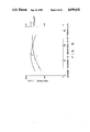
- FIG. 1A is a plane view of one such prior art planar inductor
- FIG. 1B is a sectional view of the inductor as taken along line A--A of FIG. 1A.
- Insulating layers 3a, 3b and 3c are formed of a dielectric or the like. Coils 1a and 1b are connected electrically to each other via through hole 4, and form an inductor between terminals 5a and 5b at their respective end portions.
- Spiral conductor coils 1a and 1b, insulating layers 3a, 3b and 3c, and ferromagnetic ribbons 2a and 2b, which constitute the planar inductor, must be bonded together.
- insulating layers 3a, 3b and 3c are formed from an organic polymer, for example, the individual layers may be bonded by being pressurized at a temperature not lower than the softening point of the material, or otherwise, the contact portions between the elements may be bonded by means of a suitable bonding agent.
- magnetostriction of ferromagnetic ribbons 2a and 2b is substantial, however, compressive stress or other stress acts on the surfaces of the ribbons while adjacent insulating layers 3a, 3b and 3c are being bonded. Interactions of the stress and the magnetostriction deteriorates the magnetic characteristics, thereby lowering the effective permeability. If ferromagnetic ribbons 2a and 2b are subject to strain during use of the completed planar inductor, the effective permeability also changes, so that the inductance may possibly vary. The higher the permeability, the more noticeable these phenomena will be.
- the planar inductor may be applied to an output-side choke coil of a DC-DC converter or the like.
- a high-frequency current superposed with a DC current flows through the planar inductor. Therefore, the inductor requires a good DC superposition characteristic.
- the conventional planar inductors have not, however, a very good DC superposition characteristic. If this characteristic of the inductor is poor, the inductance lowers, so that the control becomes difficult. Accordingly, the efficiency of the DC-DC converter lowers. Thus, it is not appropriate to apply the plane inductor directly to the DC-DC converter and the like.
- An object of the present invention is to provide a planar inductor in which inductance is prevented from lowering as its components are bonded together, so that the inductance value per unit volume is increased.
- Another object of the invention is to provide a planar inductor enjoying a small thickness and a higher inductor value per unit volume.
- Still another object of the invention is to provide a planar inductor having a good DC superposition characteristic.
- a planar inductor which has spiral conductor coil means sandwiched between ferromagnetic layers with insulating layers interposed therebetween, and is characterized in that the spiral conductor coil means is formed of two spiral conductor coils of the same shape arranged flush with and close to each other, the two spiral conductor coils are connected electrically to each other so that currents of different directions flow through the conductor coils, and the spiral conductor coil means is sandwiched between the two ferromagnetic layers with the insulating layers therebetween, each of the ferromagnetic layers having an area greater than the combined area of the two conductor coils.
- the absolute value of magnetostriction of each ferromagnetic layer is 1 ⁇ 10 -6 or less.
- the ferromagnetic layers are formed of an amorphous magnetic alloy.
- the average thickness of each ferromagnetic layer ranges from 4 to 20 ⁇ m.
- the ferromagnetic layers should preferably be formed of a ribbon- or film-shaped high-permeability amorphous alloy which has recently started to attract public attention.
- the ferromagnetic layers should have a composition given by
- M is at least one of elements selected from the group including Ti, V, Cr, Cu, Zr, Ni, Nb, Mo, Hf, Ta, W, and platinum metals, and a, b, , and y are values within ranges given by
- Fe is an element for adjusting the magnetostriction to 0, and M is an element used to improve the thermal stability of the permeability. Since the thermal stability can be improved by setting value b within the range from 0.3 to 0.7, x may be 0. Value x is restricted within the range 0 ⁇ x ⁇ 0.08 because the Curie temperature is too low to be practical if x exceeds 0.08. Si and B are elements essential to noncrystallization. Value y is restricted within the range 15 ⁇ y ⁇ 35 because the thermal stability is too poor if y is less than 15, and because the Curie temperature is too low to be practical if y exceeds 35. Mixture ratio b between Si and B is restricted within 0.3 ⁇ b ⁇ 0.7 because the thermal stability of the magnetic characteristic is particularly good in that case.
- the path of magnetic flux is allowed to exit only in a gap portion in the center of the spiral conductor coil means, so that the inductance per unit volume can be increased, and the inductance of the whole planar inductor can be prevented from lowering.
- the inductance can be prevented from lowering due to stress or the like which may be produced when the components of the planar inductor are bonded together.
- the inductance value per unit volume (L/V) can be prevented from being reduced. If the thickness of the ferromagnetic layer is less than 4 ⁇ m, the layer cannot enjoy a sectional area large enough for the passage of all the magnetic flux which is produced as the currents flow through the spiral conductor coils. Thus, leakage flux increases, so that the inductance lowers considerably, and therefore, inductance value L/V per unit volume is reduced. If the thickness of the ferromagnetic exceeds 20 ⁇ m, on the other hand, the sectional area of the layer in a magnetic circuit becomes large enough to allow the passage of all the magnetic flux produced in the aforesaid manner. Thus, the magnetic resistance is reduced, so that the leakage flux lessens, and the inductance increases. Since the volume of the planar inductor also increases, however, value L/V is rather reduced.
- a planar inductor which has spiral conductor coil means sandwiched between ferromagnetic layers with insulating layers interposed therebetween, and is characterized in that a ferromagnetic substance is disposed flush with and/or in the central portion of the spiral conductor coil means, and in a region surrounding the outer periphery of the spiral conductor coil means, so that the ferromagnetic substance is at least partially in contact with the ferromagnetic layers.
- the ferromagnetic substance consists essentially of a compact of ferromagnet powder or a composite including ferromagnetic powder.
- the magnetic resistance is reduced at the central and peripheral portions of the spiral conductor coil means, so that the inductance per unit volume can be increased, and the inductance of the whole planar inductor can be prevented from lowering.
- a planar inductor which has spiral conductor coil means sandwiched between ferromagnetic layers with insulating layers interposed therebetween, and is characterized in that a ferromagnetic substance is disposed flush with and/or in the central portion of the spiral conductor coil means, and in a region surrounding the outer periphery of the spiral conductor coil means.
- the magnetic resistance is reduced at the central and peripheral portions of the spiral conductor coil means, so that the inductance per unit volume can be increased, and the inductance of the whole planar inductor can be prevented from lowering.
- a planar inductor which comprises a plurality of layers of spiral conductor coil means stacked with insulating layers therebetween, and is characterized in that the spiral conductor coil means are electrically connected in series with one another so that currents of the same direction flow through the conductor coil means, and a laminated structure including the spiral conductor coil means and the insulating layers is sandwiched between ferromagnetic layers with insulating layers interposed therebetween.
- Each spiral conductor coil means of the planar inductor is generally composed of a two-layer spiral conductor coil assembly in which spiral coils on either side of each insulating layer are connected via a through hole. Unless there is a hindrance to the removal of terminals, the spiral conductor coil means may be composed of only one spiral coil.
- the average thickness of each ferromagnetic layer ranges from 4 to 20 ⁇ m.
- the ratio (t/l) of the thickness (t) of the ferromagnetic layer to the side length (l) thereof is preferably 1 ⁇ 10 -3 or more.
- laminate planar inductors may be classified into two types. According to type I, a plurality of planar inductors, each having a construction such that spiral conductor coil means is sandwiched between ferromagnetic layers with insulating layers interposed between them, are stacked in layers. Type II is constructed so that a plurality of spiral conductor coil means are stacked with insulating layers between them, and the laminated structure is sandwiched between ferromagnetic layers with insulating layers interposed between them. In type I, two insulating layers and two ferromagnetic layers exist between each two adjacent conductor coil means. In type II, on the other hand, only the insulating layer exists between each two adjacent coil means.
- the planar inductor according to the present invention (type II) is generally thinner than the planar inductor of type I, and has substantially same general inductance value as type I.
- the inductance value per unit volume is greater.
- the planar inductor of this type moreover, reduction of the inductance value per unit volume (L/V) can be prevented by restricting the average thickness of each ferromagnetic layer within the range from 4 to 20 ⁇ m. If the thickness of the ferromagnetic layer is less than 4 ⁇ m, the layer cannot enjoy a sectional area large enough for the passage of all the magnetic flux which is produced as the currents flow through the spiral conductor coils. Thus, leakage flux increases, so that the inductance lowers considerably, and inductance value L/V per unit volume is reduced.
- the sectional area of the layer in the magnetic circuit becomes large enough to allow the passage of all the magnetic flux produced in the aforesaid manner.
- the magnetic resistance is reduced, so that the leakage flux lessens, and the inductance increases. Since the volume of the planar inductor also increases, however, value L/V is rather reduced.
- the ratio (t/l) of the thickness (t) of the ferromagnetic layer to the side length (l) thereof is preferably 1 ⁇ 10-3 or more for the following reason.
- a DC current is superposed, so that the planar inductor requires a good DC superposition characteristic.
- the superposed DC current is estimated at 0.2 A or more.
- the magnetic flux is supposed to flow in the planar direction of the ferromagnetic layers.
- the coefficient of planar diamagnetic field of the ferromagnetic layers influences the planar magnetic resistance. More specifically, if the coefficient of diamagnetic field is greater, then the magnetic resistance increases in proportion. Thus, the increase of the magnetic resistance produces the same effect as a planar magnetic gap, thereby improving the DC superposition characteristic of the inductance.
- a high-permeability amorphous alloy should be used for the ferromagnetic layers.
- a square planar inductor for example, if the ratio of the thickness of each ferromagnetic layer to the side length thereof is greater, then the coefficient of planar diamagnetic field of the ferromagnetic layer increases in proportion. In other words, the greater the thickness of the ferromagnetic layer, or the shorter the side length, the greater the coefficient of diamagnetic field is. If the ratio between the thickness and the side length is 10 -3 or more, the magnetic resistance increases, so that the DC superposition characteristic of the inductance is improved.
- the spiral conductor coils or a laminated structure thereof and, therefore, the ferromagnetic layers on either side thereof are circular in shape, the magnetic resistance increases, thus improving the DC superposition characteristic of the inductance, when the ratio of the thickness of each ferromagnetic layer to the diameter thereof is 10 -3 or more.
- a laminated structure including a plurality of ferromagnetic ribbons may be used as the ferromagnetic layer, for example. The same effect may be also obtained with use of a planar inductor which has no laminate construction.
- a planar inductor which comprises spiral conductor coil means or a laminated structure including a plurality of spiral conductor coil means sandwiched between ferromagnetic layers each including a plurality of ferromagnetic ribbons, each of the ferromagnetic ribbons having a thickness of 100 ⁇ m or less.
- the magnetic flux flows in the planar direction of the ferromagnetic layers. Therefore, if each ferromagnetic layer is formed of a plurality of ferromagnetic ribbons stacked in layers, as in this planar inductor, the general thickness of the ferromagnetic layer becomes greater, so that planar diamagnetic fields increase. Thus, the magnetic resistance can be enhanced, thereby improving the DC superposition characteristic of the inductance.
- the spiral conductor coils may be stacked in layers. In this case, however, it is advisable to dispose only the insulating layers between the conductor coils, without interposing the ferromagnetic layers. This is because the existence of the ferromagnetic layers between the conductor coils is hardly conducive to the increase of the inductance, and instead, causes the general thickness of the planar inductor to increase, thereby lowering the inductance per unit volume.
- the thickness of each of the ferromagnetic ribbons constituting each ferromagnetic layer is adjusted to 100 ⁇ m less for the following reason.
- the planar inductor when applying the planar inductor to a DC-DC converter or the like which is used with a frequency of 10 kHz or more, if the ribbon thickness exceeds 100 ⁇ m, the magnetic flux is prevented from penetrating the ferromagnetic layer by a skin effect.
- the inductance cannot increase in proportion to the increase of the thickness of the ferromagnetic ribbon, so that the inductance per unit volume is rather reduced.
- the thickness of each ferromagnetic ribbon should be 4 ⁇ m or more.
- the ribbon thickness is less than 4 ⁇ m, the ribbon cannot enjoy a sectional area large enough for the passage of all the magnetic flux which is produced as the currents flow through the spiral conductor coils. Thus, leakage flux increases, so that the inductance lowers considerably, and therefore, the inductance value per unit volume is reduced.
- a plurality of ferromagnetic ribbons are used to form each ferromagnetic layer because the DC superposition characteristic cannot be improved with use of only one ribbon for each ferromagnetic layer, as in the case of the prior art planar inductors.
- the ferromagnetic ribbons used in each ferromagnetic layer are increased in number, the DC superposition characteristic is improved considerably. If the number exceeds ten, however, the effect of improvement is reduced. Thus, the volume increases for nothing, so that the inductance per unit volume lowers.
- two to ten ferromagnetic ribbons are used for the purpose.
- the ratio of the thickness (t) of each ferromagnetic layer, composed of a plurality of ferromagnetic ribbons to the side length should range from 2 ⁇ 10 -3 to 1 ⁇ 10 -2 .
- a square planar inductor for example, if the ratio of the thickness of each ferromagnetic layer to the side length thereof is greater, then the coefficient of planar diamagnetic field of the ferromagnetic layer increases in proportion. In other words, the greater the thickness of the ferromagnetic layer, or the shorter the side length, the greater the coefficient of diamagnetic field is. If the ratio between the thickness and the side length ranges from 2 ⁇ 10 -3 to 1 ⁇ 10 -2 , the magnetic resistance increases, so that the DC superposition characteristic of the inductance can be improved.
- the spiral conductor coils or a laminated structure thereof and, therefore, the ferromagnetic layers on either side thereof are circular in shape, the magnetic resistance increases, thus improving the DC superposition characteristic of the inductance, when the ratio of the thickness of each ferromagnetic layer to the diameter thereof ranges from 2 ⁇ 10 -3 to 1 ⁇ 10 -2 .
- FIG. 1A is a plane view of a prior art planar inductor
- FIG. 1B is a sectional view of the prior art planar inductor as taken along line A--A of FIG. 1A;
- FIG. 2 is a diagram for illustrating flux paths of the prior art planar inductor
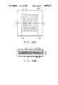
- FIG. 3A is a plane view of a planar inductor according to a first embodiment of the present invention.
- FIG. 3B is a sectional view of the planar inductor of the first embodiment as taken along line A--A of FIG. 3A;
- FIG. 4 is a diagram for illustrating a flux path of the planar inductor of the first embodiment
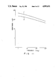
- FIG. 5 shows characteristic curves indicative of relationships between the inductance and the frequency of the planar inductor
- FIG. 6 shows characteristic curves indicative of a relationship between the inductance of the planar inductor of the first embodiment and the average thickness of a ferromagnetic ribbon and a relationship between the inductance per unit volume (L/V) and the average ribbon thickness;
- FIG. 7A is a plane view of a plan view of a planar inductor according to a second embodiment of the present invention.
- FIG. 7B is a sectional view of the planar inductor of the second embodiment as taken along line A--A of FIG. 7A;
- FIG. 8 is a diagram for illustrating flux paths of the planar inductor of the second embodiment
- FIGS. 9, 11 and 14 show characteristic curves indicative of relationships between the inductance and frequency of the planar inductor of the second embodiment
- FIGS. 10A, 12A and 15A are plane views of planar inductors according to third, fourth, and fifth embodiments of the present invention, respectively;
- FIGS. 10B, 12B and 15B are sectional views of the planar inductors of the third, fourth, and fifth embodiments as taken along lines A--A of FIGS. 10A, 12A and 15A, respectively;
- FIG. 13 is a diagram for illustrating flux paths of the planar inductor according to the fourth embodiment shown in FIG. 12;
- FIG. 16A is a plane view of a planar inductor according to a sixth embodiment of the present invention.
- FIG. 16B is a sectional view of the planar inductor of the sixth embodiment as taken along line A--A of FIG. 16A;
- FIG. 17 shows characteristic curves indicative of relationships between the respective inductances of the planar inductor of the sixth embodiment (Embodiment 6) and a planar inductor of Comparative Example 7 and the average ribbon thickness;
- FIG. 18 shows characteristic curves indicative of relationships between the inductance per unit volume (L/V) of the planar inductors of Embodiment 6 and Comparative Example 7 and the average ribbon thickness;
- FIG. 19 is a sectional view of a planar inductor according to a seventh embodiment of the present invention.
- FIG. 20 is a sectional view of a planar inductor prepared as a comparative example for the seventh embodiment
- FIG. 21 shows characteristic curves indicative of the frequency characteristics of inductances L of the planar inductors of the seventh embodiment and the comparative example
- FIG. 22 shows characteristic curves indicative of the frequency characteristics of the respective inductors per unit volume (L/V) of the planar inductors of the seventh embodiment and the comparative example;
- FIG. 23 shows characteristic curves indicative of relationships between the superposed DC current and the inductance of the planar inductor of the seventh embodiment, obtained with use of the number of amorphous alloy ribbons as a parameter;
- FIG. 24 shows characteristic curves indicative of relationships between the superposed DC current and the ratio of the inductance produced when the superposed DC voltage is applied to the inductance produced when the superposed DC voltage is not applied, with respect to the planar inductor of the seventh embodiment, obtained with use of the number of amorphous alloy ribbons as the parameter;
- FIG. 25 shows a characteristic curve indicative of a relationship between the ratio of the thickness of the amorphous alloy ribbon to the side length thereof and the ratio of the inductance produced when a superposed DC current of 0.2 A is applied to the inductance produced when the superposed DC current is not applied, with respect to the planar inductor of the seventh embodiment;
- FIG. 26A is a plane view of a planar inductor according to an eighth embodiment of the present invention.
- FIG. 26B is a sectional view as taken along line A--A' of FIG. 26A;
- FIG. 27 shows characteristic curves indicative of relationships between the superposed DC current and the inductance of the planar inductor of the eighth embodiment, obtained with use of the number of ferromagnetic ribbons as a parameter;
- FIG. 28 shows a characteristic curve indicative of a relationship between the ratio of the thickness of the laminate of the ferromagnetic layers to the side length thereof and the ratio of the inductance produced when a superposed DC current of 0.2 A is applied to the inductance produced when the superposed DC current is not applied, with respect to the planar inductor of the eighth embodiment.
- FIG. 3A is a plane view of a planar inductor according to a first embodiment of tHe present invention
- FIG. 3B is a sectional view of the planar inductor as taken along line A--A of FIG. 3A.
- like reference numerals are used to designate the same portions as are included in the prior art planar inductor shown in FIG. 1.
- the planar inductor of this embodiment is constructed so that two pairs of spiral conductor coils 1a, 1b, 1a' and 1b' of the same shape, each arranged in two layers, are situated flush with and close to each other, with insulating layers 3a, 3b and 3c alternately interposed between the layers.
- Ferromagnetic ribbons 2a and 2b which have an area wider than the area covered by the conductor coils, are pasted individually on the opposite sides of the coil assembly, with insulating layers 3a and 3c between them.
- Conductor coils 1a, 1b, 1a' and 1b' are connected electrically to one another so that currents of opposite directions flow through each two adjacent coils.
- Spiral conductor coils 1a, 1b, 1a' and 1b' are each formed of a two-layer coil which, obtained by etching a copper foil of 20 ⁇ m thickness, for example, has a 1-mm width, 1-mm coil pitch, and 10 turns.
- Insulating layers 3a, 3b and 3c are each formed of a polycarbonate sheet of 20 ⁇ m thickness, for example.
- Ferromagnetic ribbons 2a and 2b are each composed of a sheet of 25 mm by 55 mm which is obtained by cutting down a Co-based amorphous alloy ribbon (with effective permeability of about 1.2 ⁇ 10 4 at kHz and zero or nearly zero magnetostriction) having a thickness of about 16 ⁇ m and a width of 25 mm.
- the alloy ribbon may, for example, be formed by single rolling.
- the components including spiral conductor coils 1a, 1b, 1a' and 1b', are assembled by being kept at a temperature of 170° C. and a pressure of 5 kg/cm 2 for about 10 minutes, for example.
- the planar inductor of Embodiment 1 as compared with the two series-connected planar inductors of Comparative Example 1, was found to have a greater inductance value throughout the frequency band and, therefore, an improved inductance value per unit volume, thus enjoying very high efficiency.
- Alternative planar inductors for comparison were prepared. These inductors have the same construction as those of Comparative Example 1, except that the ferromagnetic ribbons are formed of an Fe-based amorphous alloy with magnetostriction of about 8 ⁇ 10 -6 .
- the inductance of the inductors of Comparative Example 2 was substantially halved when they are bent slightly. In contrast with this, the planar inductor of Embodiment 1 hardly exhibited any change although they were bent in the same manner. Thus, it was revealed that the inductance value of the planar inductor of Embodiment 1 is stable even though the inductor is subjected to a stress produced while the components are being bonded together or a bending moment during use.
- spiral conductor coils 1a, 1b, 1a' and 1b' which are formed by etching a thick copper foil of 35 ⁇ m thickness, have a width of 0.25 mm, coil pitch of 0.25 mm, 40 turns, and external size of 20 mm by 20 mm.
- These coils are arranged in two layers so that insulating layer 3b, formed of a polyimide film of 25 ⁇ m thickness, is interposed between the layers, and are connected to one another through a through hole in the center.
- a polyimide film of 12 ⁇ m thickness is used for insulating layers 3a and 3c.
- Ferromagnetic ribbons 2a and 2b which have an external size of 25 mm by 55 mm each, are obtained by cutting down four Co-based amorphous alloy ribbons with different average thicknesses, ranging from 5 to 25 ⁇ m, the alloy ribbons being formed by simple rolling and having a composition as follows:
- the effective permeability of this Co-based amorphous alloy is 2 ⁇ 10 4 (1 kHz) or 1 ⁇ 10 4 (100 kHz).
- FIG. 6 shows the dependence of the inductance (L) on the thickness of ferromagnetic ribbons 2a and 2b and the dependence of the inductance value per unit volume (L/V) on the ribbon thickness, with respect to the planar inductors described above.
- inductance L tends to increase as the average thickness of ferromagnetic ribbons 2a and 2b increases, while value L/V has a maximum when the average ribbon thickness ranges from about 10 to 15 ⁇ m.
- the ribbon thickness should range from 4 to 20 ⁇ m, preferably from 10 to 15 ⁇ m.
- FIG. 7A is a plane view of a planar inductor according to the second embodiment
- FIG. 7B is a sectional view of the inductor as taken along line A--A of FIG. 7A.
- the planar inductor of this embodiment is constructed so that two pairs of spiral conductor coils 1a and 1b of the same shape are arranged in two layers, with insulating layers 3a, 3b and 3c alternately interposed between the layers.
- Ferromagnetic ribbons 2a and 2b which have an area wider than the area covered by the conductor coils, are pasted individually on the opposite sides of the coil assembly, with insulating layers 3a and 3c between them.
- Ferromagnetic substance 10 is disposed in the center of the coil assembly so as to be in contact with ferromagnetic ribbons 2a and 2b.
- Spiral conductor coils 1a and 1b are each formed of a two-layer coil which, obtained by etching a copper foil of 20 ⁇ m thickness, for example, has a 1-mm width, 1-mm coil pitch, and 10 turns.
- Insulating layers 3a, 3b and 3c are each formed of a polycarbonate sheet of 20 ⁇ m thickness, for example.
- Ferromagnetic ribbons 2a and 2b are each composed of a sheet of 25 mm by 25 mm which is obtained by cutting down a Co-based amorphous alloy ribbon (with effective permeability of about 1.2 ⁇ 10 4 at 1 kHz and zero or nearly zero magnetostriction) having a thickness of about 16 ⁇ m and a width of 25 mm.
- the alloy ribbon may, for example, be formed by single rolling.
- Ferromagnetic substance 10 is composed of four or five pieces of 2 mm by 2 mm which are obtained by cutting down a Co-based amorphous alloy ribbon, for example.
- the components, including spiral conductor coils 1a and 1b, are assembled by being kept at a temperature of 170° C. and a pressure of 5 kg/cm 2 for about 10 minutes, for example.
- the planar inductor of Embodiment 2 in which the gap portion in the center of the coil assembly is short-circuited by means of ferromagnetic substance 10 set therein, was found to have a greater inductance value throughout the frequency band and, therefore, an improved inductance value per unit volume, as compared with Comparative Example 3, thus enjoying very high efficiency.
- An alternative planar inductor for comparison (Comparative Example 4) was prepared.
- This inductor has the same construction as that of Comparative Example 3, except that the ferromagnetic ribbons are formed of an Fe-based amorphous alloy with magnetostriction of about 8 ⁇ 10 -6 .
- the inductance of the inductor of Comparative Example 4 was substantially deteriorated when they are bent slightly.
- the planar inductor of Embodiment 2 hardly exhibited any change although they were bent in the same manner.
- the inductance value of the planar inductor of Embodiment 2 is stable even though the inductor is subjected to a stress produced while the components are being bonded together or a bending moment during use.
- a planar inductor according to Embodiment 3 was manufactured, as shown in FIG. 10.
- two planar inductors of Embodiment 2 are arranged so that two pairs of spiral conductor coils 1a, 1b, 1a' and 1b' are situated flush with and close to each other.
- Ferromagnetic ribbons 2a and 2b which have an area wider than the area covered by the conductor coils, are pasted individually on the opposite sides of the coil assembly, with insulating layers 3a and 3c between them.
- Conductor coils 1a, 1b, 1a' and 1b' are connected electrically to one another so that currents of opposite directions flow through each two adjacent coils.
- Characteristic curve I' of FIG. 11 represents the result of the examination.
- the planar inductor of Embodiment 3 as compared with Comparative Example 5, was found to have a greater inductance value throughout the frequency band and, therefore, an improved inductance value per unit volume.
- a planar inductor according to Embodiment 4 was manufactured, as shown in FIG. 12.
- This inductor has the same construction as that of Comparative Example 5, except that ferromagnetic substance 10" is disposed flush with spiral conductor coils 1a and 1b so as to surround the outer periphery of the coil assembly.
- a planar inductor composed of the same spiral conductor coils, insulating layers, and ferromagnetic ribbons as are used in Embodiment 4, was formed having a gap portion without a ferromagnetic substance surrounding the outer periphery of the coil assembly (Comparative Example 6).
- the frequency characteristic of this comparative example was also examined.
- Curve II" of FIG. 14 represents the examination result.
- the planar inductor of Embodiment 4 as compared with Comparative Example 6, was found to have a greater inductance value throughout the frequency band and, therefore, an improved inductance value per unit volume.
- a planar inductor according to Embodiment 5 was manufactured, as shown in FIG. 15.
- ferromagnetic substance 10' covers those regions where insulating layers 3a and 3c, just inside ferromagnetic ribbons 2a and 2b, respectively, are removed.
- the planar inductor of this embodiment as compared with Embodiment 4, was found to have a further greater inductance value throughout the frequency band and, therefore, an improved inductance value per unit volume.
- planar inductor with the configuration shown in FIG. 16.
- ferromagnetic substance 10 is disposed in the center of an assembly of spiral conductor coils 1a and 1b, while ferromagnetic substance 10'" is disposed in the region surrounding the outer periphery of the coil assembly.
- conductor coils 1a and 1b which are formed by etching a thick copper foil of 35 ⁇ m thickness, have a width of 0.25 mm, coil pitch of 0.25 mm, 40 turns, and external size of 20 mm by 20 mm.
- insulating layer 3b formed of a polyimide film of 25 ⁇ m thickness, is interposed between the layers, and are connected to one another through a through hole in the center.
- a polyimide film of 12 ⁇ m thickness is used for insulating layers 3a and 3c.
- Ferromagnetic ribbons 2a and 2b which have an external size of 25 mm by 25 mm each, are obtained by cutting down five Co-based amorphous alloy ribbons with different average thicknesses, ranging from 5 to 25 ⁇ m, the alloy ribbons being formed by simple rolling and having a composition as follows:
- the effective permeability of this Co-based amorphous alloy is 2 ⁇ 10 4 (1 kHz) or 1 ⁇ 10 4 (100 kHz).
- Ferromagnetic substance 10 which is disposed in the center of the coil assembly, is formed of six ribbons in layers which, having an external size of 2 mm by 2 mm, are obtained by cutting down a Co-based amorphous alloy having the aforesaid composition and an average thickness of 20 ⁇ m.
- Ferromagnetic substance 10' which is disposed outside the outer periphery of spiral conductor coils 1a and 1b, is formed of six frame-shaped ribbons in layers which, having an internal size (indicated by X in FIG. 16A) of 21 mm and an external size (indicated by Y) of 25 mm, are obtained by cutting down a Co-based amorphous alloy having the aforesaid composition and an average thickness of 20 ⁇ m.
- FIG. 17 shows the dependence of the inductance (L) on the thickness of ferromagnetic ribbons 2a and 2b
- FIG. 18 shows the dependence of the inductance value per unit volume (L/V) on the ribbon thickness, with respect to the planar inductors of the different configurations prepared in the aforesaid manner.
- full- and broken-line curves represent results for the planar inductors of Embodiment 6 and Comparative Example 7, respectively.
- inductance L tends to increase as the average thickness of ferromagnetic ribbons 2a and 2b increases, while value L/V has a maximum when the average ribbon thickness ranges from about 10 to 15 ⁇ m, without regard to the presence of ferromagnetic substances 10 and 10'".
- ferromagnetic substances 10 and 10' are disposed in the center of and outside the outer periphery of the coil assembly, both L and L/V are much greater than when the ferromagnetic substances are not used at all.
- the ribbon thickness should range from 4 to 20 ⁇ m, preferably from 10 to 15 ⁇ m.
- FIG. 19 is a sectional view of a planar inductor according to Embodiment 7 of the present invention
- FIG. 20 is a sectional view of a planar inductor prepared as a comparative example for comparison therewith.
- the plane view of the inductor resembles FIG. 1A and, therefore, is omitted.
- each spiral conductor coil assembly 1 is formed of spiral coils 1a and 1b with an external size of 20 mm by 20 mm, width of 250 ⁇ m, coil pitch of 500 ⁇ m, and 40 turns (20 turns on each side).
- Coils 1a and 1b are obtained by forming a both-sided FPC board, which includes a polyimide film (insulating layer 3b) of 25 ⁇ m thickness and Cu foils of 35 ⁇ m thickness formed on either side thereof and connected to each other through center through hole 4, and then etching the Cu foils.
- each of these inductors includes spiral conductor coil assembly 1, which is sandwiched between two 25-mm square ribbons (ferromagnetic layers 2a and 2b) 18 ⁇ m thick, with polyimide films (insulating layers 3a and 3c) of 7 ⁇ m between the coil assembly and their corresponding ribbons.
- Coil assembly 1 is composed of spiral coils 1a and 1b , with an external size of 20 mm by 20 mm, width of 250 ⁇ m, coil pitch of 500 ⁇ m, and 40 turns (20 turns on each side), and a polyimide film (insulating layer 3b) of 25 ⁇ m thickness sandwiched between the coils.
- An instantaneous bonding agent was applied to the side faces of the resulting planar inductor with the laminate construction.
- the thicknesses of the planar inductors of Embodiment 7 and Comparative Example 8 are 510 ⁇ m and 605 ⁇ m, respectively.
- FIG. 21 shows the frequency characteristic of inductance L of each planar inductor
- FIG. 22 shows that of inductance L/V per unit volume.
- inductance L of the planar inductors of Embodiment 7 and Comparative Example 8 are substantially equal.
- the inductor of Embodiment 7, which is thinner, is rather greater in inductance.
- the value of inductance L/V per unit volume of the planar inductor of Embodiment 7 is about 20% greater than that of the planar inductor of Comparative Example 7.
- the DC superposition characteristic was examined on planar inductors which have the same fundamental configuration as the one shown in FIG. 19, and in which one to ten square Co-based high-permeability amorphous alloy ribbons, having a thickness of 18 ⁇ m and a side 25 ⁇ m long, are used as ferromagnetic layers 2a and 2b.
- FIGS. 23 to 25 show results of this examination.
- FIG. 23 shows characteristic curves indicative of relationships between the superposed DC current and the inductance, obtained with use of the number of amorphous alloy ribbons as a parameter.
- FIG. 24 shows characteristic curves indicative cf relationships between the superposed DC current and the ratio of the inductance produced when the superposed DC current is applied to the inductance produced when the superposed current is not applied, obtained with use of the number of amorphous alloy ribbons as the parameter.
- FIG. 25 shows a characteristic curve indicative of a relationship between the ratio of the thickness of the laminate of the amorphous alloy ribbons to the side length thereof and the ratio of the inductance produced when a superposed DC current of 0.2 A is applied to the inductance produced when the superposed DC current is not applied. All the inductance values were measured at 50 kHz.
- inductance L 0 produced when the superposed DC current is not applied can only attain a value much smaller than n times the value obtained when n equals 1.
- number n becomes greater, then the rate of reduction of the inductance with the increase of the superposed DC current is lowered in proportion, so that the DC superposition characteristic is improved.
- the ratio (t/l) of the thickness of the ribbon laminate to the side length thereof is smaller than 10 -3 , the ratio (L 0 .2 /L 0 ) of the inductance produced when the superposed DC current of 0.2 A is applied to the inductance produced when the superposed DC current is not applied is 0.3 or less, thus indicating a poor DC superposition characteristic.
- L 0 .2 /L 0 is greater than 0.3, that is, great enough for practical use.
- L 0 .2 /L 0 is 0.8 or more, so that the DC superposition characteristic is considerably improved.
- FIG. 26A is a plane view of a planar inductor according to an eighth embodiment of the present invention
- FIG. 26B is a sectional view as taken along line A--A' of FIG. 26A.
- spiral conductor coil assembly 1 is formed of spiral coils 1a and 1b with an external size of 20 mm by 20 mm, width of 250 ⁇ m, coil pitch of 500 ⁇ m, and 40 turns (20 turns on each side).
- Coils 1a and 1b are obtained by forming a both-sided FPC board (flexible printed board), which includes a polyimide film (insulating layer 3b) of 25 ⁇ m thickness and Cu foils of 35 ⁇ m thickness formed on either side thereof and connected to each other through center through hole 4, and then etching the Cu foils.
- the planar inductor of Embodiment 8 is constructed so that conductor coil assembly 1 with the aforesaid configuration is sandwiched between two sets of ferromagnetic layers each including a plurality of square ribbons (ferromagnetic ribbons 2a and 2b) with polyimide films (insulating layers 3a and 3c) of 7 ⁇ m between the coil assembly and their corresponding sets of layers.
- Each square ribbon whose side is 25 mm long, is cut out from a Co-based high-permeability amorphous alloy ribbon which, having a average thickness of 16 ⁇ m and a width of 25 mm, is formed by simple rolling.
- An inductance is formed between terminals 5a and 5b of the planar inductor composed of these members.
- FIG. 27 shows relationships between the superposed DC current and the inductance of these planar inductors, obtained with use of the number of ferromagnetic ribbons as a parameter.
- the inductance values were measured at 50 kHz.
- FIG. 28 shows a relationship between the ratio of the thickness of the laminate of the ferromagnetic layer to the side length thereof and the ratio of the inductance (L 0 .2) produced when a superposed DC current of 0.2 A is applied to the inductance (L 0 ) produced when the superposed DC current is not applied, with respect to the aforementioned planar inductors.
- ratio t/l is smaller than 10 -3
- ratio L 0 .2 /L 0 is smaller than 0.5, thus indicating a poor DC superposition characteristic.
- t/l is 3 ⁇ 10 -3 or more
- L 0 .2 /L 0 is 0.85 or more, so that the DC superposition characteristic is considerably improved.
- a planar inductor according to the present was applied to a DC-DC converter of a 5 V/2 W type, and its efficiency was examined with use of 15 V input voltage and 0.2 A output current. Thereupon, efficiency ⁇ was found to be about 60% when n is 1, while it increased to 71% when n was increased to 5.
Abstract
Disclosed is a planar inductor which has spiral conductor coil means sandwiched between ferromagnetic layers with insulating layers interposed therebetween. The spiral conductor coil means is formed of two spiral conductor coils of the same shape arranged flush with and close to each other. Moreover, the two spiral conductor coils are connected electrically to each other so that currents of different directions flow individually through the conductor coils. Furthermore, the spiral conductor coil means is sandwiched between the two ferromagnetic layers with the insulating layers therebetween, each of the ferromagnetic layers having an area greater than the combined area of the two conductor coils. In the planar inductor according to the present invention, inductance is prevented from lowering while its components are being bonded together, so that the inductance value per unit volume is increased.
Description
1. Field of the Invention
The present invention relates to a planar inductor.
2. Description of the Related Art
Conventionally known are planar inductors in which two spiral conductor coils 1a and 1b are sandwiched between ferromagnetic ribbons 2a and 2b with insulating layers 3a, 3b and 3c alternately interposed between them, as shown in FIG. 1. FIG. 1A is a plane view of one such prior art planar inductor, and FIG. 1B is a sectional view of the inductor as taken along line A--A of FIG. 1A. Full and broken lines in the plane view of FIG. 1A, which are indicative of conductor coils 1a and 1b, respectively, correspond to the respective center lines of coils 1a and 1b shown in the sectional view of FIG. 1B. Insulating layers 3a, 3b and 3c are formed of a dielectric or the like. Coils 1a and 1b are connected electrically to each other via through hole 4, and form an inductor between terminals 5a and 5b at their respective end portions.
If a current is applied to spiral conductor coils 1a and 1b of the planar inductor, however, magnetic fluxes 6a and 6b flow in opposite directions from the center or through-hole 4, as shown in FIG. 2. As a result, gap portions 7a and 7b, where magnetic flux density is very low, exist at two positions near the central and outer peripheral portions of each conductor coil. Accordingly, the inductance is inevitably reduced. In this case, an intensive magnetic field is generated at central gap portion 73 by conductor coils 1a and 1b, while there is hardly any magnetic field at peripheral gap portion 7b. Thus, the reduction of the inductance is much greater at the peripheral portion than at the central portion.
If magnetostriction of ferromagnetic ribbons 2a and 2b is substantial, however, compressive stress or other stress acts on the surfaces of the ribbons while adjacent insulating layers 3a, 3b and 3c are being bonded. Interactions of the stress and the magnetostriction deteriorates the magnetic characteristics, thereby lowering the effective permeability. If ferromagnetic ribbons 2a and 2b are subject to strain during use of the completed planar inductor, the effective permeability also changes, so that the inductance may possibly vary. The higher the permeability, the more noticeable these phenomena will be.
In a magnetic circuit cf this planar inductor, if ferromagnetic ribbons 2a and 2b are thicker, then the magnetic resistance is generally reduced in proportion, thus increasing the inductance. However, this is inconsistent with the object to minimize the general thickness of the plane inductor.
Meanwhile, the planar inductor may be applied to an output-side choke coil of a DC-DC converter or the like. In this case, a high-frequency current superposed with a DC current flows through the planar inductor. Therefore, the inductor requires a good DC superposition characteristic.
The conventional planar inductors have not, however, a very good DC superposition characteristic. If this characteristic of the inductor is poor, the inductance lowers, so that the control becomes difficult. Accordingly, the efficiency of the DC-DC converter lowers. Thus, it is not appropriate to apply the plane inductor directly to the DC-DC converter and the like.
An object of the present invention is to provide a planar inductor in which inductance is prevented from lowering as its components are bonded together, so that the inductance value per unit volume is increased.
Another object of the invention is to provide a planar inductor enjoying a small thickness and a higher inductor value per unit volume.
Still another object of the invention is to provide a planar inductor having a good DC superposition characteristic.
According to an aspect of the present invention, there is provided a planar inductor which has spiral conductor coil means sandwiched between ferromagnetic layers with insulating layers interposed therebetween, and is characterized in that the spiral conductor coil means is formed of two spiral conductor coils of the same shape arranged flush with and close to each other, the two spiral conductor coils are connected electrically to each other so that currents of different directions flow through the conductor coils, and the spiral conductor coil means is sandwiched between the two ferromagnetic layers with the insulating layers therebetween, each of the ferromagnetic layers having an area greater than the combined area of the two conductor coils.
Preferably, the absolute value of magnetostriction of each ferromagnetic layer is 1×10⁻⁶ or less.
Preferably, moreover, the ferromagnetic layers are formed of an amorphous magnetic alloy.
Preferably, furthermore, the average thickness of each ferromagnetic layer ranges from 4 to 20 μm.
Also, the ferromagnetic layers should preferably be formed of a ribbon- or film-shaped high-permeability amorphous alloy which has recently started to attract public attention. In particular, the ferromagnetic layers should have a composition given by
(Co.sub.1-a-x Fe.sub.a M.sub.x).sub.100-y (Si.sub.1-b B.sub.b).sub.y,
where M is at least one of elements selected from the group including Ti, V, Cr, Cu, Zr, Ni, Nb, Mo, Hf, Ta, W, and platinum metals, and a, b, , and y are values within ranges given by
0.01≦a≦0.10,
0.3≦b≦0.7,
0≦x≦0.08, and
15≦y≦35,
respectively.
In the above structural formula, Fe is an element for adjusting the magnetostriction to 0, and M is an element used to improve the thermal stability of the permeability. Since the thermal stability can be improved by setting value b within the range from 0.3 to 0.7, x may be 0. Value x is restricted within the range 0≦x≦0.08 because the Curie temperature is too low to be practical if x exceeds 0.08. Si and B are elements essential to noncrystallization. Value y is restricted within the range 15≦y≦35 because the thermal stability is too poor if y is less than 15, and because the Curie temperature is too low to be practical if y exceeds 35. Mixture ratio b between Si and B is restricted within 0.3≦b≦0.7 because the thermal stability of the magnetic characteristic is particularly good in that case.
According to the planar inductor constructed in this manner, the path of magnetic flux is allowed to exit only in a gap portion in the center of the spiral conductor coil means, so that the inductance per unit volume can be increased, and the inductance of the whole planar inductor can be prevented from lowering.
By adjusting the absolute value of magnetostriction of each ferromagnetic layer to 1×10⁻⁶ or less, moreover, the inductance can be prevented from lowering due to stress or the like which may be produced when the components of the planar inductor are bonded together.
By restricting the average thickness of each ferromagnetic within the range from 4 to 20 μm, furthermore, the inductance value per unit volume (L/V) can be prevented from being reduced. If the thickness of the ferromagnetic layer is less than 4 μm, the layer cannot enjoy a sectional area large enough for the passage of all the magnetic flux which is produced as the currents flow through the spiral conductor coils. Thus, leakage flux increases, so that the inductance lowers considerably, and therefore, inductance value L/V per unit volume is reduced. If the thickness of the ferromagnetic exceeds 20 μm, on the other hand, the sectional area of the layer in a magnetic circuit becomes large enough to allow the passage of all the magnetic flux produced in the aforesaid manner. Thus, the magnetic resistance is reduced, so that the leakage flux lessens, and the inductance increases. Since the volume of the planar inductor also increases, however, value L/V is rather reduced.
According to the present invention, there is provided a planar inductor which has spiral conductor coil means sandwiched between ferromagnetic layers with insulating layers interposed therebetween, and is characterized in that a ferromagnetic substance is disposed flush with and/or in the central portion of the spiral conductor coil means, and in a region surrounding the outer periphery of the spiral conductor coil means, so that the ferromagnetic substance is at least partially in contact with the ferromagnetic layers.
Preferably, the ferromagnetic substance consists essentially of a compact of ferromagnet powder or a composite including ferromagnetic powder.
According to the planar inductor constructed in this manner, the magnetic resistance is reduced at the central and peripheral portions of the spiral conductor coil means, so that the inductance per unit volume can be increased, and the inductance of the whole planar inductor can be prevented from lowering.
According to still another aspect of the present invention, there is provided a planar inductor which has spiral conductor coil means sandwiched between ferromagnetic layers with insulating layers interposed therebetween, and is characterized in that a ferromagnetic substance is disposed flush with and/or in the central portion of the spiral conductor coil means, and in a region surrounding the outer periphery of the spiral conductor coil means.
According to the planar inductor constructed in this manner, the magnetic resistance is reduced at the central and peripheral portions of the spiral conductor coil means, so that the inductance per unit volume can be increased, and the inductance of the whole planar inductor can be prevented from lowering.
According to a further aspect of the present invention, there is provided a planar inductor which comprises a plurality of layers of spiral conductor coil means stacked with insulating layers therebetween, and is characterized in that the spiral conductor coil means are electrically connected in series with one another so that currents of the same direction flow through the conductor coil means, and a laminated structure including the spiral conductor coil means and the insulating layers is sandwiched between ferromagnetic layers with insulating layers interposed therebetween.
Each spiral conductor coil means of the planar inductor is generally composed of a two-layer spiral conductor coil assembly in which spiral coils on either side of each insulating layer are connected via a through hole. Unless there is a hindrance to the removal of terminals, the spiral conductor coil means may be composed of only one spiral coil.
Preferably, the average thickness of each ferromagnetic layer ranges from 4 to 20 μm. Moreover, the ratio (t/l) of the thickness (t) of the ferromagnetic layer to the side length (l) thereof is preferably 1×10⁻³ or more.
In general, laminate planar inductors may be classified into two types. According to type I, a plurality of planar inductors, each having a construction such that spiral conductor coil means is sandwiched between ferromagnetic layers with insulating layers interposed between them, are stacked in layers. Type II is constructed so that a plurality of spiral conductor coil means are stacked with insulating layers between them, and the laminated structure is sandwiched between ferromagnetic layers with insulating layers interposed between them. In type I, two insulating layers and two ferromagnetic layers exist between each two adjacent conductor coil means. In type II, on the other hand, only the insulating layer exists between each two adjacent coil means.
As a result of an earnest investigation by the inventors hereof, it was found that the ferromagnetic layers, existing between the adjacent spiral conductor coil means, as in the case cf type I, are hardly conducive to the increase of the inductance of the laminate planar inductors. It was also indicated that substantially the same inductance value for type I can be obtained even though only the insulating layer exists between each two adjacent spiral conductor coil means, without being accompanied by the ferromagnetic layers, as in the case of type II. Therefore, the planar inductor according to the present invention (type II) is generally thinner than the planar inductor of type I, and has substantially same general inductance value as type I. Thus, the inductance value per unit volume is greater.
According to the planar inductor of this type, moreover, reduction of the inductance value per unit volume (L/V) can be prevented by restricting the average thickness of each ferromagnetic layer within the range from 4 to 20 μm. If the thickness of the ferromagnetic layer is less than 4 μm, the layer cannot enjoy a sectional area large enough for the passage of all the magnetic flux which is produced as the currents flow through the spiral conductor coils. Thus, leakage flux increases, so that the inductance lowers considerably, and inductance value L/V per unit volume is reduced. If the thickness of the ferromagnetic layer exceeds 20 μm, on the other hand, the sectional area of the layer in the magnetic circuit becomes large enough to allow the passage of all the magnetic flux produced in the aforesaid manner. Thus, the magnetic resistance is reduced, so that the leakage flux lessens, and the inductance increases. Since the volume of the planar inductor also increases, however, value L/V is rather reduced.
In this planar inductor, the ratio (t/l) of the thickness (t) of the ferromagnetic layer to the side length (l) thereof is preferably 1×10⁻³ or more for the following reason.
Generally, when using the planar inductor according to the present invention on the output side of a DC-DC converter, a DC current is superposed, so that the planar inductor requires a good DC superposition characteristic. The superposed DC current is estimated at 0.2 A or more.
In this planar inductor, the magnetic flux is supposed to flow in the planar direction of the ferromagnetic layers. In this case, the coefficient of planar diamagnetic field of the ferromagnetic layers influences the planar magnetic resistance. More specifically, if the coefficient of diamagnetic field is greater, then the magnetic resistance increases in proportion. Thus, the increase of the magnetic resistance produces the same effect as a planar magnetic gap, thereby improving the DC superposition characteristic of the inductance. Preferably, a high-permeability amorphous alloy should be used for the ferromagnetic layers.
In a square planar inductor, for example, if the ratio of the thickness of each ferromagnetic layer to the side length thereof is greater, then the coefficient of planar diamagnetic field of the ferromagnetic layer increases in proportion. In other words, the greater the thickness of the ferromagnetic layer, or the shorter the side length, the greater the coefficient of diamagnetic field is. If the ratio between the thickness and the side length is 10-3 or more, the magnetic resistance increases, so that the DC superposition characteristic of the inductance is improved. If the spiral conductor coils or a laminated structure thereof and, therefore, the ferromagnetic layers on either side thereof are circular in shape, the magnetic resistance increases, thus improving the DC superposition characteristic of the inductance, when the ratio of the thickness of each ferromagnetic layer to the diameter thereof is 10-3 or more. In order to increase the thickness of the ferromagnetic layer, a laminated structure including a plurality of ferromagnetic ribbons may be used as the ferromagnetic layer, for example. The same effect may be also obtained with use of a planar inductor which has no laminate construction.
According to a still further aspect of the present invention, there is provided a planar inductor which comprises spiral conductor coil means or a laminated structure including a plurality of spiral conductor coil means sandwiched between ferromagnetic layers each including a plurality of ferromagnetic ribbons, each of the ferromagnetic ribbons having a thickness of 100 μm or less.
In the planar inductor constructed in this manner, the magnetic flux flows in the planar direction of the ferromagnetic layers. Therefore, if each ferromagnetic layer is formed of a plurality of ferromagnetic ribbons stacked in layers, as in this planar inductor, the general thickness of the ferromagnetic layer becomes greater, so that planar diamagnetic fields increase. Thus, the magnetic resistance can be enhanced, thereby improving the DC superposition characteristic of the inductance.
The spiral conductor coils may be stacked in layers. In this case, however, it is advisable to dispose only the insulating layers between the conductor coils, without interposing the ferromagnetic layers. This is because the existence of the ferromagnetic layers between the conductor coils is hardly conducive to the increase of the inductance, and instead, causes the general thickness of the planar inductor to increase, thereby lowering the inductance per unit volume.
In the planar inductor constructed in this manner, the thickness of each of the ferromagnetic ribbons constituting each ferromagnetic layer is adjusted to 100 μm less for the following reason. Generally, when applying the planar inductor to a DC-DC converter or the like which is used with a frequency of 10 kHz or more, if the ribbon thickness exceeds 100 μm, the magnetic flux is prevented from penetrating the ferromagnetic layer by a skin effect. Thus, the inductance cannot increase in proportion to the increase of the thickness of the ferromagnetic ribbon, so that the inductance per unit volume is rather reduced. Preferably, the thickness of each ferromagnetic ribbon should be 4 μm or more. If the ribbon thickness is less than 4 μm, the ribbon cannot enjoy a sectional area large enough for the passage of all the magnetic flux which is produced as the currents flow through the spiral conductor coils. Thus, leakage flux increases, so that the inductance lowers considerably, and therefore, the inductance value per unit volume is reduced.
In this planar inductor, moreover, a plurality of ferromagnetic ribbons are used to form each ferromagnetic layer because the DC superposition characteristic cannot be improved with use of only one ribbon for each ferromagnetic layer, as in the case of the prior art planar inductors. As the ferromagnetic ribbons used in each ferromagnetic layer are increased in number, the DC superposition characteristic is improved considerably. If the number exceeds ten, however, the effect of improvement is reduced. Thus, the volume increases for nothing, so that the inductance per unit volume lowers. Preferably, after all, two to ten ferromagnetic ribbons are used for the purpose.
For the improvement of the DC superposition characteristic, moreover, the ratio of the thickness (t) of each ferromagnetic layer, composed of a plurality of ferromagnetic ribbons to the side length, should range from 2×10⁻³ to 1×10⁻².
In a square planar inductor, for example, if the ratio of the thickness of each ferromagnetic layer to the side length thereof is greater, then the coefficient of planar diamagnetic field of the ferromagnetic layer increases in proportion. In other words, the greater the thickness of the ferromagnetic layer, or the shorter the side length, the greater the coefficient of diamagnetic field is. If the ratio between the thickness and the side length ranges from 2×10⁻³ to 1×10⁻², the magnetic resistance increases, so that the DC superposition characteristic of the inductance can be improved. If the spiral conductor coils or a laminated structure thereof and, therefore, the ferromagnetic layers on either side thereof are circular in shape, the magnetic resistance increases, thus improving the DC superposition characteristic of the inductance, when the ratio of the thickness of each ferromagnetic layer to the diameter thereof ranges from 2×10⁻³ to 1×10⁻².
FIG. 1A is a plane view of a prior art planar inductor;
FIG. 1B is a sectional view of the prior art planar inductor as taken along line A--A of FIG. 1A;
FIG. 2 is a diagram for illustrating flux paths of the prior art planar inductor;
FIG. 3A is a plane view of a planar inductor according to a first embodiment of the present invention;
FIG. 3B is a sectional view of the planar inductor of the first embodiment as taken along line A--A of FIG. 3A;
FIG. 4 is a diagram for illustrating a flux path of the planar inductor of the first embodiment;
FIG. 5 shows characteristic curves indicative of relationships between the inductance and the frequency of the planar inductor;
FIG. 6 shows characteristic curves indicative of a relationship between the inductance of the planar inductor of the first embodiment and the average thickness of a ferromagnetic ribbon and a relationship between the inductance per unit volume (L/V) and the average ribbon thickness;
FIG. 7A is a plane view of a plan view of a planar inductor according to a second embodiment of the present invention;
FIG. 7B is a sectional view of the planar inductor of the second embodiment as taken along line A--A of FIG. 7A;
FIG. 8 is a diagram for illustrating flux paths of the planar inductor of the second embodiment;
FIGS. 9, 11 and 14 show characteristic curves indicative of relationships between the inductance and frequency of the planar inductor of the second embodiment;
FIGS. 10A, 12A and 15A are plane views of planar inductors according to third, fourth, and fifth embodiments of the present invention, respectively;
FIGS. 10B, 12B and 15B are sectional views of the planar inductors of the third, fourth, and fifth embodiments as taken along lines A--A of FIGS. 10A, 12A and 15A, respectively;
FIG. 13 is a diagram for illustrating flux paths of the planar inductor according to the fourth embodiment shown in FIG. 12;
FIG. 16A is a plane view of a planar inductor according to a sixth embodiment of the present invention;
FIG. 16B is a sectional view of the planar inductor of the sixth embodiment as taken along line A--A of FIG. 16A;
FIG. 17 shows characteristic curves indicative of relationships between the respective inductances of the planar inductor of the sixth embodiment (Embodiment 6) and a planar inductor of Comparative Example 7 and the average ribbon thickness;
FIG. 18 shows characteristic curves indicative of relationships between the inductance per unit volume (L/V) of the planar inductors of Embodiment 6 and Comparative Example 7 and the average ribbon thickness;
FIG. 19 is a sectional view of a planar inductor according to a seventh embodiment of the present invention;
FIG. 20 is a sectional view of a planar inductor prepared as a comparative example for the seventh embodiment;
FIG. 21 shows characteristic curves indicative of the frequency characteristics of inductances L of the planar inductors of the seventh embodiment and the comparative example;
FIG. 22 shows characteristic curves indicative of the frequency characteristics of the respective inductors per unit volume (L/V) of the planar inductors of the seventh embodiment and the comparative example;
FIG. 23 shows characteristic curves indicative of relationships between the superposed DC current and the inductance of the planar inductor of the seventh embodiment, obtained with use of the number of amorphous alloy ribbons as a parameter;
FIG. 24 shows characteristic curves indicative of relationships between the superposed DC current and the ratio of the inductance produced when the superposed DC voltage is applied to the inductance produced when the superposed DC voltage is not applied, with respect to the planar inductor of the seventh embodiment, obtained with use of the number of amorphous alloy ribbons as the parameter;
FIG. 25 shows a characteristic curve indicative of a relationship between the ratio of the thickness of the amorphous alloy ribbon to the side length thereof and the ratio of the inductance produced when a superposed DC current of 0.2 A is applied to the inductance produced when the superposed DC current is not applied, with respect to the planar inductor of the seventh embodiment;
FIG. 26A is a plane view of a planar inductor according to an eighth embodiment of the present invention;
FIG. 26B is a sectional view as taken along line A--A' of FIG. 26A;
FIG. 27 shows characteristic curves indicative of relationships between the superposed DC current and the inductance of the planar inductor of the eighth embodiment, obtained with use of the number of ferromagnetic ribbons as a parameter; and
FIG. 28 shows a characteristic curve indicative of a relationship between the ratio of the thickness of the laminate of the ferromagnetic layers to the side length thereof and the ratio of the inductance produced when a superposed DC current of 0.2 A is applied to the inductance produced when the superposed DC current is not applied, with respect to the planar inductor of the eighth embodiment.
Preferred embodiments of the present invention will now be described with reference to the accompanying drawings.
FIG. 3A is a plane view of a planar inductor according to a first embodiment of tHe present invention, and FIG. 3B is a sectional view of the planar inductor as taken along line A--A of FIG. 3A. In these drawings, like reference numerals are used to designate the same portions as are included in the prior art planar inductor shown in FIG. 1. The planar inductor of this embodiment is constructed so that two pairs of spiral conductor coils 1a, 1b, 1a' and 1b' of the same shape, each arranged in two layers, are situated flush with and close to each other, with insulating layers 3a, 3b and 3c alternately interposed between the layers. Ferromagnetic ribbons 2a and 2b, which have an area wider than the area covered by the conductor coils, are pasted individually on the opposite sides of the coil assembly, with insulating layers 3a and 3c between them. Conductor coils 1a, 1b, 1a' and 1b' are connected electrically to one another so that currents of opposite directions flow through each two adjacent coils.
Spiral conductor coils 1a, 1b, 1a' and 1b' are each formed of a two-layer coil which, obtained by etching a copper foil of 20 μm thickness, for example, has a 1-mm width, 1-mm coil pitch, and 10 turns.
Insulating layers 3a, 3b and 3c are each formed of a polycarbonate sheet of 20 μm thickness, for example.
The components, including spiral conductor coils 1a, 1b, 1a' and 1b', are assembled by being kept at a temperature of 170° C. and a pressure of 5 kg/cm2 for about 10 minutes, for example.
The path of magnetic flux 6 of the planar inductor (Embodiment 1) constructed in this manner is indicated by an arrowhead line in FIG. 4. The frequency characteristic of this planar inductor was actually examined. Characteristic curve I of FIG. 5 represents the result of the examination.
For comparison, two planar inductors, each composed of the same spiral conductor coils, insulating layers, and ferromagnetic ribbons as are used in Embodiment 1, were simply connected electrically in series with each other (Comparative Example 1). The frequency characteristic of this comparative example was also examined. Curve II of FIG. 5 represents the examination result. In the inductors of Comparative Example 1, each ferromagnetic ribbon measures 25 mm by 25 mm.
As seen from the results shown in FIG. 5, the planar inductor of Embodiment 1, as compared with the two series-connected planar inductors of Comparative Example 1, was found to have a greater inductance value throughout the frequency band and, therefore, an improved inductance value per unit volume, thus enjoying very high efficiency.
Alternative planar inductors for comparison (Comparative Example 2) were prepared. These inductors have the same construction as those of Comparative Example 1, except that the ferromagnetic ribbons are formed of an Fe-based amorphous alloy with magnetostriction of about 8×10⁻⁶. The inductance of the inductors of Comparative Example 2 was substantially halved when they are bent slightly. In contrast with this, the planar inductor of Embodiment 1 hardly exhibited any change although they were bent in the same manner. Thus, it was revealed that the inductance value of the planar inductor of Embodiment 1 is stable even though the inductor is subjected to a stress produced while the components are being bonded together or a bending moment during use.
Subsequently, the influence of the thickness of the ferromagnetic ribbons was examined on the planar inductor of Embodiment 1. In this case, spiral conductor coils 1a, 1b, 1a' and 1b', which are formed by etching a thick copper foil of 35 μm thickness, have a width of 0.25 mm, coil pitch of 0.25 mm, 40 turns, and external size of 20 mm by 20 mm. These coils are arranged in two layers so that insulating layer 3b, formed of a polyimide film of 25 μm thickness, is interposed between the layers, and are connected to one another through a through hole in the center. A polyimide film of 12 μm thickness is used for insulating layers 3a and 3c.
(Co.sub.0.88 Fe.sub.0.06 Ni.sub.0.04 Nb.sub.0.02).sub.75 Si.sub.10 B.sub.15.
The effective permeability of this Co-based amorphous alloy is 2×10⁴ (1 kHz) or 1×10⁴ (100 kHz).
FIG. 6 shows the dependence of the inductance (L) on the thickness of ferromagnetic ribbons 2a and 2b and the dependence of the inductance value per unit volume (L/V) on the ribbon thickness, with respect to the planar inductors described above.
As seen from FIG. 6, inductance L tends to increase as the average thickness of ferromagnetic ribbons 2a and 2b increases, while value L/V has a maximum when the average ribbon thickness ranges from about 10 to 15 μm. Thus, the ribbon thickness should range from 4 to 20 μm, preferably from 10 to 15 μm.
A second embodiment of the present invention will now be described. FIG. 7A is a plane view of a planar inductor according to the second embodiment, and FIG. 7B is a sectional view of the inductor as taken along line A--A of FIG. 7A. The planar inductor of this embodiment is constructed so that two pairs of spiral conductor coils 1a and 1b of the same shape are arranged in two layers, with insulating layers 3a, 3b and 3c alternately interposed between the layers. Ferromagnetic ribbons 2a and 2b, which have an area wider than the area covered by the conductor coils, are pasted individually on the opposite sides of the coil assembly, with insulating layers 3a and 3c between them. Ferromagnetic substance 10 is disposed in the center of the coil assembly so as to be in contact with ferromagnetic ribbons 2a and 2b.
Spiral conductor coils 1a and 1b are each formed of a two-layer coil which, obtained by etching a copper foil of 20 μm thickness, for example, has a 1-mm width, 1-mm coil pitch, and 10 turns.
Insulating layers 3a, 3b and 3c are each formed of a polycarbonate sheet of 20μm thickness, for example.
The components, including spiral conductor coils 1a and 1b, are assembled by being kept at a temperature of 170° C. and a pressure of 5 kg/cm2 for about 10 minutes, for example.
The path of magnetic flux 6 of the planar inductor (Embodiment 2) constructed in this manner is indicated by an arrowhead line in FIG. 8. The frequency characteristic of this planar inductor was actually examined. Characteristic curve I of FIG. 9 represents the result of the examination.
For comparison, a planar inductor, composed of the same spiral conductor coils, insulating layers, and ferromagnetic ribbons as are used in Embodiment 2, was formed having a gap portion without a ferromagnetic substance in the center of the coil assembly (Comparative Example 3). The frequency characteristic of this comparative example was also examined. Curve II of FIG. 9 represents the examination result.
As seen from the results shown in FIG. 9, the planar inductor of Embodiment 2, in which the gap portion in the center of the coil assembly is short-circuited by means of ferromagnetic substance 10 set therein, was found to have a greater inductance value throughout the frequency band and, therefore, an improved inductance value per unit volume, as compared with Comparative Example 3, thus enjoying very high efficiency.
An alternative planar inductor for comparison (Comparative Example 4) was prepared. This inductor has the same construction as that of Comparative Example 3, except that the ferromagnetic ribbons are formed of an Fe-based amorphous alloy with magnetostriction of about 8×10⁻⁶. The inductance of the inductor of Comparative Example 4 was substantially deteriorated when they are bent slightly. In contrast with this, the planar inductor of Embodiment 2 hardly exhibited any change although they were bent in the same manner. Thus, it was revealed that the inductance value of the planar inductor of Embodiment 2 is stable even though the inductor is subjected to a stress produced while the components are being bonded together or a bending moment during use.
A planar inductor according to Embodiment 3 was manufactured, as shown in FIG. 10. In this embodiment, two planar inductors of Embodiment 2 are arranged so that two pairs of spiral conductor coils 1a, 1b, 1a' and 1b' are situated flush with and close to each other. Ferromagnetic ribbons 2a and 2b, which have an area wider than the area covered by the conductor coils, are pasted individually on the opposite sides of the coil assembly, with insulating layers 3a and 3c between them. Conductor coils 1a, 1b, 1a' and 1b' are connected electrically to one another so that currents of opposite directions flow through each two adjacent coils. The frequency characteristic of this planar inductor was actually examined. Characteristic curve I' of FIG. 11 represents the result of the examination.
For comparison, a planar inductor, composed of the same spiral conductor coils, insulating layers, and ferromagnetic ribbons as are used in Embodiment 3, was formed having a gap portion without a ferromagnetic substance in the center of the coil assembly (Comparative Example 5). The frequency characteristic of this comparative example was also examined. Curve II' of FIG. 11 represents the examination result.
As seen from the results shown n FIG. 11, the planar inductor of Embodiment 3, as compared with Comparative Example 5, was found to have a greater inductance value throughout the frequency band and, therefore, an improved inductance value per unit volume.
A planar inductor according to Embodiment 4 was manufactured, as shown in FIG. 12. This inductor has the same construction as that of Comparative Example 5, except that ferromagnetic substance 10" is disposed flush with spiral conductor coils 1a and 1b so as to surround the outer periphery of the coil assembly.
The path of magnetic flux 6 of the planar inductor (Embodiment 4) constructed in this manner is indicated by an arrowhead line in FIG. 13. The frequency characteristic of this planar inductor was actually examined. Characteristic curve I" of FIG. 14 represents the result of the examination.
For comparison, a planar inductor, composed of the same spiral conductor coils, insulating layers, and ferromagnetic ribbons as are used in Embodiment 4, was formed having a gap portion without a ferromagnetic substance surrounding the outer periphery of the coil assembly (Comparative Example 6). The frequency characteristic of this comparative example was also examined. Curve II" of FIG. 14 represents the examination result.
As seen from the results shown in FIG. 14, the planar inductor of Embodiment 4, as compared with Comparative Example 6, was found to have a greater inductance value throughout the frequency band and, therefore, an improved inductance value per unit volume.
A planar inductor according to Embodiment 5 was manufactured, as shown in FIG. 15. In this inductor, ferromagnetic substance 10'" covers those regions where insulating layers 3a and 3c, just inside ferromagnetic ribbons 2a and 2b, respectively, are removed. The planar inductor of this embodiment, as compared with Embodiment 4, was found to have a further greater inductance value throughout the frequency band and, therefore, an improved inductance value per unit volume.
The influence of the thickness of the ferromagnetic ribbons was examined on the planar inductor with the configuration shown in FIG. 16. In this planar inductor, ferromagnetic substance 10 is disposed in the center of an assembly of spiral conductor coils 1a and 1b, while ferromagnetic substance 10'" is disposed in the region surrounding the outer periphery of the coil assembly. In this case, conductor coils 1a and 1b, which are formed by etching a thick copper foil of 35 μm thickness, have a width of 0.25 mm, coil pitch of 0.25 mm, 40 turns, and external size of 20 mm by 20 mm.
These coils are arranged in two layers so that insulating layer 3b, formed of a polyimide film of 25 μm thickness, is interposed between the layers, and are connected to one another through a through hole in the center. A polyimide film of 12 μm thickness is used for insulating layers 3a and 3c.
(Co.sub.0.88 Fe.sub.0.06 Ni.sub.0.04 Nb.sub.0.02).sub.75 Si.sub.10 B.sub.15.
The effective permeability of this Co-based amorphous alloy is 2×10⁴ (1 kHz) or 1×10⁴ (100 kHz).
For comparison, five planar inductors (Comparative Example 7) were prepared. These inductors, whose ferromagnetic ribbons 2a and 2b are different in average thickness, have the same construction as aforesaid, except that neither of ferromagnetic substances is disposed in the center of or outside the outer periphery of the coil assembly.
FIG. 17 shows the dependence of the inductance (L) on the thickness of ferromagnetic ribbons 2a and 2b, and FIG. 18 shows the dependence of the inductance value per unit volume (L/V) on the ribbon thickness, with respect to the planar inductors of the different configurations prepared in the aforesaid manner. In FIGS. 17 and 18, full- and broken-line curves represent results for the planar inductors of Embodiment 6 and Comparative Example 7, respectively.
As seen from FIGS. 17 and 18, inductance L tends to increase as the average thickness of ferromagnetic ribbons 2a and 2b increases, while value L/V has a maximum when the average ribbon thickness ranges from about 10 to 15 μm, without regard to the presence of ferromagnetic substances 10 and 10'". When ferromagnetic substances 10 and 10'"are disposed in the center of and outside the outer periphery of the coil assembly, both L and L/V are much greater than when the ferromagnetic substances are not used at all. Thus, the ribbon thickness should range from 4 to 20 μm, preferably from 10 to 15 μm.
It was ascertained that the same results as are shown in FIGS. 17 and 18 can be obtained from the planar inductor of Embodiment 3 (FIG. 10) in which the two spiral conductor coils are arranged flush with each other and electrically connected so that currents of opposite directions flow through the coils.
FIG. 19 is a sectional view of a planar inductor according to Embodiment 7 of the present invention, and FIG. 20 is a sectional view of a planar inductor prepared as a comparative example for comparison therewith. In either case, the plane view of the inductor resembles FIG. 1A and, therefore, is omitted. In FIGS. 19 and 20, each spiral conductor coil assembly 1 is formed of spiral coils 1a and 1b with an external size of 20 mm by 20 mm, width of 250 μm, coil pitch of 500 μm, and 40 turns (20 turns on each side). Coils 1a and 1b are obtained by forming a both-sided FPC board, which includes a polyimide film (insulating layer 3b) of 25 μm thickness and Cu foils of 35 μm thickness formed on either side thereof and connected to each other through center through hole 4, and then etching the Cu foils.
In manufacturing the planar inductor of Embodiment 7, as shown in FIG. 19, three conductor coil assemblies 1 with the aforementioned configuration were stacked in layers with polyimide films (insulating layers 3d) of 7 μm thickness between them. The resulting laminated structure was sandwiched between two square ribbons ( ferromagnetic layers 2a and 2b) with polyimide films (insulating layers 3e and 3f) of 7 μm between the laminated structure and their corresponding ribbons. Each square ribbon, whose side is 25 mm long, was cut out from a Co-based high-permeability amorphous alloy ribbon which, having a thickness of 18 μm and a width of 25 mm, was formed by simple rolling. An instantaneous bonding agent was applied to the side faces of the resulting planar inductor with the laminate construction, in order to bond the individual layers together.
For comparison, three planar inductors (Comparative Example 8) were stacked in layers, as shown in FIG. 20. Each of these inductors includes spiral conductor coil assembly 1, which is sandwiched between two 25-mm square ribbons ( ferromagnetic layers 2a and 2b) 18 μm thick, with polyimide films (insulating layers 3a and 3c) of 7 μm between the coil assembly and their corresponding ribbons. Coil assembly 1 is composed of spiral coils 1a and 1b , with an external size of 20 mm by 20 mm, width of 250 μm, coil pitch of 500 μm, and 40 turns (20 turns on each side), and a polyimide film (insulating layer 3b) of 25 μm thickness sandwiched between the coils. An instantaneous bonding agent was applied to the side faces of the resulting planar inductor with the laminate construction.
In either of the planar inductors of Embodiment 7 and Comparative Example 8, three spiral conductor coil assemblies 1 are connected to one another so that currents of the same phase flow through them.
The thicknesses of the planar inductors of Embodiment 7 and Comparative Example 8 are 510 μm and 605 μm, respectively.
FIG. 21 shows the frequency characteristic of inductance L of each planar inductor, and FIG. 22 shows that of inductance L/V per unit volume.
As seen from FIG. 21, the values of inductance L of the planar inductors of Embodiment 7 and Comparative Example 8 are substantially equal. On the high-frequency side, however, the inductor of Embodiment 7, which is thinner, is rather greater in inductance.
As seen from FIG. 22, moreover, the value of inductance L/V per unit volume of the planar inductor of Embodiment 7 is about 20% greater than that of the planar inductor of Comparative Example 7.
The DC superposition characteristic was examined on planar inductors which have the same fundamental configuration as the one shown in FIG. 19, and in which one to ten square Co-based high-permeability amorphous alloy ribbons, having a thickness of 18 μm and a side 25 μm long, are used as ferromagnetic layers 2a and 2b. FIGS. 23 to 25 show results of this examination.
FIG. 23 shows characteristic curves indicative of relationships between the superposed DC current and the inductance, obtained with use of the number of amorphous alloy ribbons as a parameter. FIG. 24 shows characteristic curves indicative cf relationships between the superposed DC current and the ratio of the inductance produced when the superposed DC current is applied to the inductance produced when the superposed current is not applied, obtained with use of the number of amorphous alloy ribbons as the parameter. FIG. 25 shows a characteristic curve indicative of a relationship between the ratio of the thickness of the laminate of the amorphous alloy ribbons to the side length thereof and the ratio of the inductance produced when a superposed DC current of 0.2 A is applied to the inductance produced when the superposed DC current is not applied. All the inductance values were measured at 50 kHz.
As shown in FIG. 23, even if the number (n) of ribbons is increased, inductance L0 produced when the superposed DC current is not applied can only attain a value much smaller than n times the value obtained when n equals 1. As seen from FIGS. 23 and 24, however, if number n becomes greater, then the rate of reduction of the inductance with the increase of the superposed DC current is lowered in proportion, so that the DC superposition characteristic is improved.
As seen from FIG. 25, moreover, if the ratio (t/l) of the thickness of the ribbon laminate to the side length thereof is smaller than 10-3, the ratio (L0.2 /L0) of the inductance produced when the superposed DC current of 0.2 A is applied to the inductance produced when the superposed DC current is not applied is 0.3 or less, thus indicating a poor DC superposition characteristic. If t/l is 10-3 or more, on the other hand, L0.2 /L0 is greater than 0.3, that is, great enough for practical use. If t/l exceeds 3.5×10⁻³ moreover, L0.2 /L0 is 0.8 or more, so that the DC superposition characteristic is considerably improved.
FIG. 26A is a plane view of a planar inductor according to an eighth embodiment of the present invention, and FIG. 26B is a sectional view as taken along line A--A' of FIG. 26A. In FIG. 26, spiral conductor coil assembly 1 is formed of spiral coils 1a and 1b with an external size of 20 mm by 20 mm, width of 250 μm, coil pitch of 500 μm, and 40 turns (20 turns on each side). Coils 1a and 1b are obtained by forming a both-sided FPC board (flexible printed board), which includes a polyimide film (insulating layer 3b) of 25 μm thickness and Cu foils of 35 μm thickness formed on either side thereof and connected to each other through center through hole 4, and then etching the Cu foils. The planar inductor of Embodiment 8 is constructed so that conductor coil assembly 1 with the aforesaid configuration is sandwiched between two sets of ferromagnetic layers each including a plurality of square ribbons ( ferromagnetic ribbons 2a and 2b) with polyimide films (insulating layers 3a and 3c) of 7 μm between the coil assembly and their corresponding sets of layers. Each square ribbon, whose side is 25 mm long, is cut out from a Co-based high-permeability amorphous alloy ribbon which, having a average thickness of 16 μm and a width of 25 mm, is formed by simple rolling. An inductance is formed between terminals 5a and 5b of the planar inductor composed of these members.
For comparison, a conventional planar inductor (Comparative Example 9), which includes only one ferromagnetic ribbon on each side of the coil assembly, was prepared using the same materials as aforesaid.
FIG. 27 shows relationships between the superposed DC current and the inductance of these planar inductors, obtained with use of the number of ferromagnetic ribbons as a parameter. The inductance values were measured at 50 kHz.
As seen from FIG. 27, if number n becomes greater, then the rate of reduction of the inductance with the increase of the superposed DC current is lowered in proportion, so that the DC superposition characteristic is improved. If n is 15, however, substantially the same result is obtained as in the case where n is 10. Thus, it is indicated that the improvement effect of the DC superposition characteristic hardly makes any change if the ferromagnetic ribbons used exceed ten in number.
FIG. 28 shows a relationship between the ratio of the thickness of the laminate of the ferromagnetic layer to the side length thereof and the ratio of the inductance (L0.2) produced when a superposed DC current of 0.2 A is applied to the inductance (L0) produced when the superposed DC current is not applied, with respect to the aforementioned planar inductors.
As seen from FIG. 28, if ratio t/l is smaller than 10-3, ratio L0.2 /L0 is smaller than 0.5, thus indicating a poor DC superposition characteristic. If t/l is 3×10⁻³ or more, on the other hand, L0.2 /L0 is 0.85 or more, so that the DC superposition characteristic is considerably improved.
Furthermore, a planar inductor according to the present was applied to a DC-DC converter of a 5 V/2 W type, and its efficiency was examined with use of 15 V input voltage and 0.2 A output current. Thereupon, efficiency η was found to be about 60% when n is 1, while it increased to 71% when n was increased to 5.
Claims (4)
1. A planar inductor comprising a laminated structure including a plurality of spiral conductor coil means sandwiched between ferromagnetic layers each including a plurality of ferromagnetic ribbons, each said ferromagnetic ribbon having a thickness of 100 μm or less.
2. A planar inductor according to claim 1, comprising:
insulating layers interposed between said plural spiral conductor coil means and said ferromagnetic layers;
said spiral conductor coil means electrically connected in series with one another so that currents of the same direction flow through the conductor coil means; and
each of said plural spiral conductor coil means stacked with insulating layers therebetween to form a stacked structure, said stacked structure disposed between said ferromagnetic layers, wherein the ferromagnetic ribbons of each layer are separated by insulating layers.
3. A planar inductor according to claim 2, wherein the thickness of each ferromagnetic ribbon falls within the range between 4 and 100 μm.
4. A planar inductor according to claim 2, wherein a ratio of the thickness of each ferromagnetic layer, composed of a plurality of ferromagnetic ribbons, to the side length falls within the range of between 2×10⁻³ and 1×10⁻².
Applications Claiming Priority (12)
| Application Number | Priority Date | Filing Date | Title |
|---|---|---|---|
| JP24547287 | 1987-09-29 | ||
| JP62-245473 | 1987-09-29 | ||
| JP24547387 | 1987-09-29 | ||
| JP62-245472 | 1987-09-29 | ||
| JP63-62262 | 1988-03-16 | ||
| JP63-62261 | 1988-03-16 | ||
| JP63062261A JPH01157507A (en) | 1987-09-29 | 1988-03-16 | Plane inductor |
| JP6226288A JPH01157508A (en) | 1987-09-29 | 1988-03-16 | Plane inductor |
| JP63142043A JP2958892B2 (en) | 1988-06-09 | 1988-06-09 | Planar inductor |
| JP63-142043 | 1988-06-09 | ||
| JP63151779A JP2958893B2 (en) | 1988-06-20 | 1988-06-20 | Planar inductor |
| JP63-151779 | 1988-06-20 |
Publications (1)
| Publication Number | Publication Date |
|---|---|
| US4959631A true US4959631A (en) | 1990-09-25 |
Family
ID=27550882
Family Applications (1)
| Application Number | Title | Priority Date | Filing Date |
|---|---|---|---|
| US07/250,401 Expired - Lifetime US4959631A (en) | 1987-09-29 | 1988-09-28 | Planar inductor |
Country Status (4)
| Country | Link |
|---|---|
| US (1) | US4959631A (en) |
| EP (1) | EP0310396B1 (en) |
| KR (1) | KR910003292B1 (en) |
| DE (1) | DE3854177T2 (en) |
Cited By (153)
| Publication number | Priority date | Publication date | Assignee | Title |
|---|---|---|---|---|
| US5083236A (en) * | 1990-09-28 | 1992-01-21 | Motorola, Inc. | Inductor structure with integral components |
| US5142767A (en) * | 1989-11-15 | 1992-09-01 | Bf Goodrich Company | Method of manufacturing a planar coil construction |
| US5157576A (en) * | 1990-02-20 | 1992-10-20 | Tdk Corporation | Composite electric part of stacked multi-layer structure |
| US5250923A (en) * | 1992-01-10 | 1993-10-05 | Murata Manufacturing Co., Ltd. | Laminated chip common mode choke coil |
| US5302932A (en) * | 1992-05-12 | 1994-04-12 | Dale Electronics, Inc. | Monolythic multilayer chip inductor and method for making same |
| DE4306416A1 (en) * | 1993-03-02 | 1994-09-08 | Kolbe & Co Hans | Coil structure for a printed circuit board arrangement |
| US5349743A (en) * | 1991-05-02 | 1994-09-27 | At&T Bell Laboratories | Method of making a multilayer monolithic magnet component |
| US5363080A (en) * | 1991-12-27 | 1994-11-08 | Avx Corporation | High accuracy surface mount inductor |
| US5376774A (en) * | 1992-11-13 | 1994-12-27 | Electric Power Research Institute | Low emission induction heating coil |
| US5387551A (en) * | 1992-03-04 | 1995-02-07 | Kabushiki Kaisha Toshiba | Method of manufacturing flat inductance element |
| US5414401A (en) * | 1992-02-20 | 1995-05-09 | Martin Marietta Corporation | High-frequency, low-profile inductor |
| US5430613A (en) * | 1993-06-01 | 1995-07-04 | Eaton Corporation | Current transformer using a laminated toroidal core structure and a lead frame |
| EP0706304A1 (en) | 1994-10-09 | 1996-04-10 | Menu-System Ernst Wüst | Cooker |
| US5515022A (en) * | 1991-05-13 | 1996-05-07 | Tdk Corporation | Multilayered inductor |
| US5548265A (en) * | 1992-02-28 | 1996-08-20 | Fuji Electric Co., Ltd. | Thin film magnetic element |
| US5572179A (en) * | 1992-05-27 | 1996-11-05 | Fuji Electric Co., Ltd. | Thin film transformer |
| US5572779A (en) * | 1994-11-09 | 1996-11-12 | Dale Electronics, Inc. | Method of making an electronic thick film component multiple terminal |
| US5583424A (en) * | 1993-03-15 | 1996-12-10 | Kabushiki Kaisha Toshiba | Magnetic element for power supply and dc-to-dc converter |
| US5583474A (en) * | 1990-05-31 | 1996-12-10 | Kabushiki Kaisha Toshiba | Planar magnetic element |
| US5639391A (en) * | 1990-09-24 | 1997-06-17 | Dale Electronics, Inc. | Laser formed electrical component and method for making the same |
| WO1998005048A1 (en) * | 1996-07-29 | 1998-02-05 | Motorola Inc. | Low radiation planar inductor/transformer and method |
| US5849355A (en) * | 1996-09-18 | 1998-12-15 | Alliedsignal Inc. | Electroless copper plating |
| US5874883A (en) * | 1995-07-18 | 1999-02-23 | Nec Corporation | Planar-type inductor and fabrication method thereof |
| US5896078A (en) * | 1994-03-28 | 1999-04-20 | Alps Electric Co., Ltd. | Soft magnetic alloy thin film and plane-type magnetic device |
| US5900797A (en) * | 1994-11-28 | 1999-05-04 | Murata Manufacturing Co., Ltd. | Coil assembly |
| US5969590A (en) * | 1997-08-05 | 1999-10-19 | Applied Micro Circuits Corporation | Integrated circuit transformer with inductor-substrate isolation |
| US6002161A (en) * | 1995-12-27 | 1999-12-14 | Nec Corporation | Semiconductor device having inductor element made of first conductive layer of spiral configuration electrically connected to second conductive layer of insular configuration |
| US6067002A (en) * | 1995-09-12 | 2000-05-23 | Murata Manufacturing Co., Ltd. | Circuit substrate with a built-in coil |
| US6073339A (en) * | 1996-09-20 | 2000-06-13 | Tdk Corporation Of America | Method of making low profile pin-less planar magnetic devices |
| US6121852A (en) * | 1997-07-15 | 2000-09-19 | Kabushiki Kaisha Toshiba | Distributed constant element using a magnetic thin film |
| US6175293B1 (en) * | 1988-09-30 | 2001-01-16 | Kabushiki Kaisha Toshiba | Planar inductor |
| US6249205B1 (en) * | 1998-11-20 | 2001-06-19 | Steward, Inc. | Surface mount inductor with flux gap and related fabrication methods |
| US6255932B1 (en) * | 1994-03-31 | 2001-07-03 | Murata Manufacturing Co., Ltd. | Electronic component having built-in inductor |
| US6281778B1 (en) * | 1997-10-31 | 2001-08-28 | National Scientific Corp. | Monolithic inductor with magnetic flux lines guided away from substrate |
| US6293001B1 (en) | 1994-09-12 | 2001-09-25 | Matsushita Electric Industrial Co., Ltd. | Method for producing an inductor |
| US6380835B1 (en) * | 1999-07-27 | 2002-04-30 | Informaton And Communications University | Symmetric multi-layer spiral inductor for use in RF integrated circuits |
| WO2002065492A2 (en) | 2001-01-19 | 2002-08-22 | Intel Corporation | Integrated transformer |
| US6448879B1 (en) * | 1997-12-18 | 2002-09-10 | Murata Manufacturing Co., Ltd. | Coil component |
| US20030005572A1 (en) * | 1999-11-23 | 2003-01-09 | Gardner Donald S. | Integrated inductor |
| US20030042569A1 (en) * | 1999-02-26 | 2003-03-06 | Micron Technology, Inc. | Open pattern inductor |
| US20030048167A1 (en) * | 2001-08-29 | 2003-03-13 | Matsushita Electric Industrial Co., Ltd. | Magnetic device, method for manufacturing the same, and power supply module equipped with the same |
| US6593847B2 (en) * | 2000-05-22 | 2003-07-15 | The Furukawa Electric Co., Ltd. | Planar acoustic converting apparatus |
| US20030151486A1 (en) * | 1994-09-12 | 2003-08-14 | Eiichi Uriu | Inductor and method for producing the same |
| US20030210122A1 (en) * | 2002-05-13 | 2003-11-13 | Joel Concord | Inductance with a midpoint |
| US20040222492A1 (en) * | 2003-05-05 | 2004-11-11 | Gardner Donald S. | On-die micro-transformer structures with magnetic materials |
| US20040227608A1 (en) * | 2003-05-16 | 2004-11-18 | Toshifumi Nakatani | Mutual induction circuit |
| US6838970B2 (en) * | 1999-02-26 | 2005-01-04 | Memscap | Inductor for integrated circuit |
| US20050017837A1 (en) * | 1999-11-23 | 2005-01-27 | Gardner Donald S. | Integrated transformer |
| US20050035836A1 (en) * | 2001-05-30 | 2005-02-17 | Sensopad Technologies Limited | Sensing apparatus and method |
| US20050077993A1 (en) * | 2003-04-24 | 2005-04-14 | Hiroshi Kanno | High-frequency circuit |
| US20050140486A1 (en) * | 2003-12-26 | 2005-06-30 | Hung-Wen Lin | Multi-layer chip inductive element |
| US20050195061A1 (en) * | 2004-03-03 | 2005-09-08 | Atheros Communications, Inc. | Inductor layout using step symmetry for inductors |
| US20050231752A1 (en) * | 2004-04-16 | 2005-10-20 | Nokia Corporation | Image data transfer system and method |
| US20050271147A1 (en) * | 2004-06-03 | 2005-12-08 | Timothy Dupuis | Transformer isolator for digital power supply |
| US20050271148A1 (en) * | 2004-06-03 | 2005-12-08 | Timothy Dupuis | RF isolator with differential input/output |
| US20050269657A1 (en) * | 2004-06-03 | 2005-12-08 | Timothy Dupuis | On chip transformer isolator |
| US20050271149A1 (en) * | 2004-06-03 | 2005-12-08 | Timothy Dupuis | RF isolator for isolating voltage sensing and gate drivers |
| US20050272378A1 (en) * | 2004-06-03 | 2005-12-08 | Timothy Dupuis | Spread spectrum isolator |
| US20060119351A1 (en) * | 2002-10-16 | 2006-06-08 | Tt Electronics Technology Limited | Sensing apparatus and method |
| US20060125472A1 (en) * | 2002-10-16 | 2006-06-15 | Tt Electronics Technology Limited | Position sensing apparatus and method |
| US20060140168A1 (en) * | 2004-12-23 | 2006-06-29 | Samsung Electronics Co., Ltd. | Electric power-generating apparatus and method |
| US20060152323A1 (en) * | 2001-09-19 | 2006-07-13 | International Rectifier Corporation | Embedded inductor for semiconductor device circuit |
| US20060186983A1 (en) * | 2003-06-30 | 2006-08-24 | International Business Machines Corporation | On-chip inductor with magnetic core |
| US20060197642A1 (en) * | 2005-03-04 | 2006-09-07 | Michael Hargrove | Variable inductor technique |
| US20060244464A1 (en) * | 2003-02-17 | 2006-11-02 | Sensopad Limited | Sensing apparatus and method |
| US20060250155A1 (en) * | 2003-04-30 | 2006-11-09 | Baoxing Chen | Signal isolators using micro-transformers |
| US20060273872A1 (en) * | 2005-06-01 | 2006-12-07 | Intel Corporation | Power transformer |
| US20070001762A1 (en) * | 2005-06-30 | 2007-01-04 | Gerhard Schrom | DC-DC converter switching transistor current measurement technique |
| US20070030108A1 (en) * | 2004-07-15 | 2007-02-08 | Hitoshi Ishimoto | Inductance component and manufacturing method thereof |
| DE102005039379A1 (en) * | 2005-08-19 | 2007-03-01 | Fraunhofer-Gesellschaft zur Förderung der angewandten Forschung e.V. | Microelectronics inductor formed by sandwiching planar spiral coil in soft magnetic material, connects edges and center of magnetic substrates, to complete magnetic circuit |
| US20080025450A1 (en) * | 2004-06-03 | 2008-01-31 | Silicon Laboratories Inc. | Multiplexed rf isolator circuit |
| US20080031286A1 (en) * | 2004-06-03 | 2008-02-07 | Silicon Laboratories Inc. | Multiplexed rf isolator |
| US20080030080A1 (en) * | 1997-10-23 | 2008-02-07 | Baoxing Chen | Chip-scale coils and isolators based thereon |
| US20080136442A1 (en) * | 2006-07-06 | 2008-06-12 | Baoxing Chen | Signal isolator using micro-transformers |
| US20080180204A1 (en) * | 2007-01-30 | 2008-07-31 | Stmicroelectronics S.A. | Multiple-level inductance |
| US20080204116A1 (en) * | 2004-08-09 | 2008-08-28 | Sensopad Limited | Sensing Apparatus And Method |
| US20080317106A1 (en) * | 2004-06-03 | 2008-12-25 | Silicon Laboratories Inc. | Mcu with integrated voltage isolator and integrated galvanically isolated asynchronous serial data link |
| US20090027243A1 (en) * | 2004-06-03 | 2009-01-29 | Silicon Laboratories Inc. | Mcu with integrated voltage isolator to provide a galvanic isolation between input and output |
| US20090067398A1 (en) * | 2004-03-03 | 2009-03-12 | Green Michael R | Implementing Location Awareness In WLAN Devices |
| US20090171346A1 (en) * | 2007-12-28 | 2009-07-02 | Greg Leyh | High conductivity inductively equalized electrodes and methods |
| US20090243028A1 (en) * | 2004-06-03 | 2009-10-01 | Silicon Laboratories Inc. | Capacitive isolation circuitry with improved common mode detector |
| US20090306647A1 (en) * | 2008-06-05 | 2009-12-10 | Greg Leyh | Dynamically controllable multi-electrode apparatus & methods |
| US20100001823A1 (en) * | 2005-12-07 | 2010-01-07 | Mitsugu Kawarai | Flexible Coil |
| US20100022999A1 (en) * | 2008-07-24 | 2010-01-28 | Gollnick David A | Symmetrical rf electrosurgical system and methods |
| US20100052826A1 (en) * | 2004-06-03 | 2010-03-04 | Silicon Laboratories Inc. | Isolator with complementary configurable memory |
| US20100144063A1 (en) * | 2008-12-09 | 2010-06-10 | Nec Electronics Corporation | Seminconductor device |
| US20110156854A1 (en) * | 2007-10-12 | 2011-06-30 | Via Technologies, Inc. | Spiral Inductor Device |
| US8169108B2 (en) | 2004-06-03 | 2012-05-01 | Silicon Laboratories Inc. | Capacitive isolator |
| US8172835B2 (en) | 2008-06-05 | 2012-05-08 | Cutera, Inc. | Subcutaneous electric field distribution system and methods |
| US8198951B2 (en) | 2004-06-03 | 2012-06-12 | Silicon Laboratories Inc. | Capacitive isolation circuitry |
| US20130069750A1 (en) * | 2009-03-09 | 2013-03-21 | Nucurrent Inc. | System Using Multi-Layer Wire Structure for High Efficiency Wireless Communication |
| US20130068499A1 (en) * | 2011-09-15 | 2013-03-21 | Nucurrent Inc. | Method for Operation of Multi-Layer Wire Structure for High Efficiency Wireless Communication |
| US8451032B2 (en) | 2010-12-22 | 2013-05-28 | Silicon Laboratories Inc. | Capacitive isolator with schmitt trigger |
| US20130257575A1 (en) * | 2012-04-03 | 2013-10-03 | Alexander Timashov | Coil having low effective capacitance and magnetic devices including same |
| CN103765533A (en) * | 2011-08-26 | 2014-04-30 | 罗姆股份有限公司 | Magnetic metal substrate and inductance element |
| US8717136B2 (en) | 2012-01-10 | 2014-05-06 | International Business Machines Corporation | Inductor with laminated yoke |
| US20140145816A1 (en) * | 2011-09-07 | 2014-05-29 | Tdk Corporation | Laminated coil component |
| US8754500B2 (en) * | 2012-08-29 | 2014-06-17 | International Business Machines Corporation | Plated lamination structures for integrated magnetic devices |
| US20140333406A1 (en) * | 2013-05-07 | 2014-11-13 | Samsung Electro-Mechanics Co., Ltd. | Common mode filter and method of manufacturing the same |
| US20150091683A1 (en) * | 2013-09-27 | 2015-04-02 | Taiwan Semiconductor Manufacturing Company, Ltd. | Slow wave inductive structure and method of forming the same |
| US9035423B1 (en) * | 2013-12-25 | 2015-05-19 | Mitsubishi Electric Corporation | Semiconductor device with inductor having interleaved windings for controlling capacitance |
| US9064628B2 (en) | 2012-05-22 | 2015-06-23 | International Business Machines Corporation | Inductor with stacked conductors |
| CN104871307A (en) * | 2012-12-19 | 2015-08-26 | 瑞萨电子株式会社 | Semiconductor device |
| US20150270055A1 (en) * | 2014-03-20 | 2015-09-24 | Shinko Electric Industries Co., Ltd. | Inductor and Coil Substrate |
| US9208942B2 (en) | 2009-03-09 | 2015-12-08 | Nucurrent, Inc. | Multi-layer-multi-turn structure for high efficiency wireless communication |
| US9232893B2 (en) | 2009-03-09 | 2016-01-12 | Nucurrent, Inc. | Method of operation of a multi-layer-multi-turn structure for high efficiency wireless communication |
| US9293997B2 (en) | 2013-03-14 | 2016-03-22 | Analog Devices Global | Isolated error amplifier for isolated power supplies |
| US9300046B2 (en) | 2009-03-09 | 2016-03-29 | Nucurrent, Inc. | Method for manufacture of multi-layer-multi-turn high efficiency inductors |
| US9306358B2 (en) | 2009-03-09 | 2016-04-05 | Nucurrent, Inc. | Method for manufacture of multi-layer wire structure for high efficiency wireless communication |
| DE102014221568A1 (en) * | 2014-10-23 | 2016-04-28 | Siemens Aktiengesellschaft | Transformer and method for operating a transformer |
| US9439287B2 (en) | 2009-03-09 | 2016-09-06 | Nucurrent, Inc. | Multi-layer wire structure for high efficiency wireless communication |
| US9444213B2 (en) | 2009-03-09 | 2016-09-13 | Nucurrent, Inc. | Method for manufacture of multi-layer wire structure for high efficiency wireless communication |
| US9502168B1 (en) * | 2013-11-15 | 2016-11-22 | Altera Corporation | Interleaved T-coil structure and a method of manufacturing the T-coil structure |
| US9660848B2 (en) | 2014-09-15 | 2017-05-23 | Analog Devices Global | Methods and structures to generate on/off keyed carrier signals for signal isolators |
| US20170178782A1 (en) * | 2015-12-17 | 2017-06-22 | Rockwell Automation Technologies, Inc. | Compact inductor |
| US9941729B2 (en) | 2015-08-07 | 2018-04-10 | Nucurrent, Inc. | Single layer multi mode antenna for wireless power transmission using magnetic field coupling |
| US9941743B2 (en) | 2015-08-07 | 2018-04-10 | Nucurrent, Inc. | Single structure multi mode antenna having a unitary body construction for wireless power transmission using magnetic field coupling |
| US9941590B2 (en) | 2015-08-07 | 2018-04-10 | Nucurrent, Inc. | Single structure multi mode antenna for wireless power transmission using magnetic field coupling having magnetic shielding |
| US9948129B2 (en) | 2015-08-07 | 2018-04-17 | Nucurrent, Inc. | Single structure multi mode antenna for wireless power transmission using magnetic field coupling having an internal switch circuit |
| US9960628B2 (en) | 2015-08-07 | 2018-05-01 | Nucurrent, Inc. | Single structure multi mode antenna having a single layer structure with coils on opposing sides for wireless power transmission using magnetic field coupling |
| US9960629B2 (en) | 2015-08-07 | 2018-05-01 | Nucurrent, Inc. | Method of operating a single structure multi mode antenna for wireless power transmission using magnetic field coupling |
| US9998301B2 (en) | 2014-11-03 | 2018-06-12 | Analog Devices, Inc. | Signal isolator system with protection for common mode transients |
| US10063100B2 (en) | 2015-08-07 | 2018-08-28 | Nucurrent, Inc. | Electrical system incorporating a single structure multimode antenna for wireless power transmission using magnetic field coupling |
| US10270630B2 (en) | 2014-09-15 | 2019-04-23 | Analog Devices, Inc. | Demodulation of on-off-key modulated signals in signal isolator systems |
| US10283257B2 (en) * | 2016-01-08 | 2019-05-07 | Qualcomm Incorporated | Skewed co-spiral inductor structure |
| US10290608B2 (en) | 2016-09-13 | 2019-05-14 | Allegro Microsystems, Llc | Signal isolator having bidirectional diagnostic signal exchange |
| US10419251B2 (en) | 2002-09-18 | 2019-09-17 | Infineon Technologies | Digital signal transfer using integrated transformers with electrical isolation |
| US10424969B2 (en) | 2016-12-09 | 2019-09-24 | Nucurrent, Inc. | Substrate configured to facilitate through-metal energy transfer via near field magnetic coupling |
| US10536309B2 (en) | 2014-09-15 | 2020-01-14 | Analog Devices, Inc. | Demodulation of on-off-key modulated signals in signal isolator systems |
| US10636563B2 (en) | 2015-08-07 | 2020-04-28 | Nucurrent, Inc. | Method of fabricating a single structure multi mode antenna for wireless power transmission using magnetic field coupling |
| US10658847B2 (en) | 2015-08-07 | 2020-05-19 | Nucurrent, Inc. | Method of providing a single structure multi mode antenna for wireless power transmission using magnetic field coupling |
| DE102019102576A1 (en) * | 2019-02-01 | 2020-08-06 | RF360 Europe GmbH | RF filter with planar RF coil |
| US10879704B2 (en) | 2016-08-26 | 2020-12-29 | Nucurrent, Inc. | Wireless connector receiver module |
| US10903688B2 (en) | 2017-02-13 | 2021-01-26 | Nucurrent, Inc. | Wireless electrical energy transmission system with repeater |
| US10985465B2 (en) | 2015-08-19 | 2021-04-20 | Nucurrent, Inc. | Multi-mode wireless antenna configurations |
| US11056922B1 (en) | 2020-01-03 | 2021-07-06 | Nucurrent, Inc. | Wireless power transfer system for simultaneous transfer to multiple devices |
| US11115244B2 (en) | 2019-09-17 | 2021-09-07 | Allegro Microsystems, Llc | Signal isolator with three state data transmission |
| US11152151B2 (en) | 2017-05-26 | 2021-10-19 | Nucurrent, Inc. | Crossover coil structure for wireless transmission |
| US11166349B2 (en) * | 2016-03-02 | 2021-11-02 | I.R.C.A. S.P.A.—Industria Resistenze Corazzate E Affini | Induction hob and method for making induction hobs |
| US11205849B2 (en) | 2015-08-07 | 2021-12-21 | Nucurrent, Inc. | Multi-coil antenna structure with tunable inductance |
| US11227712B2 (en) | 2019-07-19 | 2022-01-18 | Nucurrent, Inc. | Preemptive thermal mitigation for wireless power systems |
| US11271430B2 (en) | 2019-07-19 | 2022-03-08 | Nucurrent, Inc. | Wireless power transfer system with extended wireless charging range |
| US11283303B2 (en) | 2020-07-24 | 2022-03-22 | Nucurrent, Inc. | Area-apportioned wireless power antenna for maximized charging volume |
| US20220113803A1 (en) * | 2016-03-31 | 2022-04-14 | Sensel, Inc. | System and method for detecting and responding to touch inputs with haptic feedback |
| US11335999B2 (en) | 2009-03-09 | 2022-05-17 | Nucurrent, Inc. | Device having a multi-layer-multi-turn antenna with frequency |
| US20220200342A1 (en) | 2020-12-22 | 2022-06-23 | Nucurrent, Inc. | Ruggedized communication for wireless power systems in multi-device environments |
| US11387040B2 (en) | 2016-12-07 | 2022-07-12 | Nitto Denko Corporation | Producing method of module |
| US11460926B2 (en) | 2016-03-31 | 2022-10-04 | Sensel, Inc. | Human-computer interface system |
| US11695302B2 (en) | 2021-02-01 | 2023-07-04 | Nucurrent, Inc. | Segmented shielding for wide area wireless power transmitter |
| US11831174B2 (en) | 2022-03-01 | 2023-11-28 | Nucurrent, Inc. | Cross talk and interference mitigation in dual wireless power transmitter |
| US11876386B2 (en) | 2020-12-22 | 2024-01-16 | Nucurrent, Inc. | Detection of foreign objects in large charging volume applications |
| US11935683B2 (en) * | 2018-12-07 | 2024-03-19 | Samsung Electro-Mechanics Co., Ltd. | Coil electronic component |
| US11972896B2 (en) | 2020-09-18 | 2024-04-30 | Virginia Tech Intellectual Properties, Inc. | Compact inductor employing redistributed magnetic flux |
Families Citing this family (16)
| Publication number | Priority date | Publication date | Assignee | Title |
|---|---|---|---|---|
| US5152480A (en) * | 1989-11-15 | 1992-10-06 | The B. F. Goodrich Company | Planar coil construction |
| DE4019241A1 (en) * | 1990-06-15 | 1991-12-19 | Telefunken Electronic Gmbh | Energy and signal transmission system - for transmitting measurement signals from vehicle tyres |
| GB2252208B (en) * | 1991-01-24 | 1995-05-03 | Burr Brown Corp | Hybrid integrated circuit planar transformer |
| US5402098A (en) * | 1991-03-25 | 1995-03-28 | Satosen Co., Ltd. | Coil |
| CA2072277A1 (en) * | 1991-07-03 | 1993-01-04 | Nobuo Shiga | Inductance element |
| EP0608127A1 (en) * | 1993-01-22 | 1994-07-27 | AT&T Corp. | Insulation system for magnetic windings having stacked planar conductors |
| US5647966A (en) * | 1994-10-04 | 1997-07-15 | Matsushita Electric Industrial Co., Ltd. | Method for producing a conductive pattern and method for producing a greensheet lamination body including the same |
| DE4442994A1 (en) | 1994-12-02 | 1996-06-05 | Philips Patentverwaltung | Planar inductance |
| KR970023498A (en) * | 1995-10-12 | 1997-05-30 | 서두칠 | Coil Assembly of Flyback Transformer |
| US6039371A (en) * | 1997-08-04 | 2000-03-21 | Smith; Mark | Vacuum stretching and gripping tool and method for laying flooring |
| JP3615024B2 (en) | 1997-08-04 | 2005-01-26 | 株式会社村田製作所 | Coil parts |
| GB2332100A (en) * | 1997-12-02 | 1999-06-09 | David Vail | An insulated winding arrangement |
| US6587025B2 (en) * | 2001-01-31 | 2003-07-01 | Vishay Dale Electronics, Inc. | Side-by-side coil inductor |
| EP1661148A2 (en) * | 2003-08-26 | 2006-05-31 | Philips Intellectual Property & Standards GmbH | Printed circuit board with integrated inductor |
| EP2779181B1 (en) * | 2013-03-12 | 2018-09-26 | NuCurrent, Inc. | Multi-layer-multi-turn structure for high efficiency inductors |
| DE102014207890A1 (en) * | 2014-04-28 | 2015-07-30 | Continental Automotive Gmbh | Foreign object detection device and power inductive charging device |
Citations (6)
| Publication number | Priority date | Publication date | Assignee | Title |
|---|---|---|---|---|
| US3833872A (en) * | 1972-06-13 | 1974-09-03 | I Marcus | Microminiature monolithic ferroceramic transformer |
| US4021705A (en) * | 1975-03-24 | 1977-05-03 | Lichtblau G J | Resonant tag circuits having one or more fusible links |
| JPS5814512A (en) * | 1981-07-17 | 1983-01-27 | Sanyo Electric Co Ltd | Inductor device |
| EP0096516A1 (en) * | 1982-06-04 | 1983-12-21 | Minnesota Mining And Manufacturing Company | Multi-turn inductor and LC network and method of construction thereof |
| US4494100A (en) * | 1982-07-12 | 1985-01-15 | Motorola, Inc. | Planar inductors |
| US4613843A (en) * | 1984-10-22 | 1986-09-23 | Ford Motor Company | Planar coil magnetic transducer |
Family Cites Families (1)
| Publication number | Priority date | Publication date | Assignee | Title |
|---|---|---|---|---|
| US4188211A (en) * | 1977-02-18 | 1980-02-12 | Tdk Electronics Company, Limited | Thermally stable amorphous magnetic alloy |
-
1988
- 1988-09-28 US US07/250,401 patent/US4959631A/en not_active Expired - Lifetime
- 1988-09-29 EP EP88309056A patent/EP0310396B1/en not_active Expired - Lifetime
- 1988-09-29 DE DE3854177T patent/DE3854177T2/en not_active Expired - Lifetime
- 1988-09-29 KR KR1019880012666A patent/KR910003292B1/en not_active IP Right Cessation
Patent Citations (6)
| Publication number | Priority date | Publication date | Assignee | Title |
|---|---|---|---|---|
| US3833872A (en) * | 1972-06-13 | 1974-09-03 | I Marcus | Microminiature monolithic ferroceramic transformer |
| US4021705A (en) * | 1975-03-24 | 1977-05-03 | Lichtblau G J | Resonant tag circuits having one or more fusible links |
| JPS5814512A (en) * | 1981-07-17 | 1983-01-27 | Sanyo Electric Co Ltd | Inductor device |
| EP0096516A1 (en) * | 1982-06-04 | 1983-12-21 | Minnesota Mining And Manufacturing Company | Multi-turn inductor and LC network and method of construction thereof |
| US4494100A (en) * | 1982-07-12 | 1985-01-15 | Motorola, Inc. | Planar inductors |
| US4613843A (en) * | 1984-10-22 | 1986-09-23 | Ford Motor Company | Planar coil magnetic transducer |
Non-Patent Citations (2)
| Title |
|---|
| IEEE Transactions on Magnetics Mag 15, No. 6, Nov. (1979) 1803 Magnetic Think Film Inductors for Integrated Circuit Applications by R. F. Soohoo. * |
| IEEE Transactions on Magnetics Mag 20, No. 5, Sep. (1984), 1804 Planer Inductor by K. Shirae et al. * |
Cited By (325)
| Publication number | Priority date | Publication date | Assignee | Title |
|---|---|---|---|---|
| US6466122B1 (en) | 1988-09-30 | 2002-10-15 | Kabushiki Kaisha Toshiba | Planar inductor |
| US6175293B1 (en) * | 1988-09-30 | 2001-01-16 | Kabushiki Kaisha Toshiba | Planar inductor |
| US5142767A (en) * | 1989-11-15 | 1992-09-01 | Bf Goodrich Company | Method of manufacturing a planar coil construction |
| US5157576A (en) * | 1990-02-20 | 1992-10-20 | Tdk Corporation | Composite electric part of stacked multi-layer structure |
| US5801521A (en) * | 1990-05-31 | 1998-09-01 | Kabushiki Kaisha Toshiba | Planar magnetic element |
| US5583474A (en) * | 1990-05-31 | 1996-12-10 | Kabushiki Kaisha Toshiba | Planar magnetic element |
| US6404317B1 (en) * | 1990-05-31 | 2002-06-11 | Kabushiki Kaisha Toshiba | Planar magnetic element |
| US6593841B1 (en) * | 1990-05-31 | 2003-07-15 | Kabushiki Kaisha Toshiba | Planar magnetic element |
| US5639391A (en) * | 1990-09-24 | 1997-06-17 | Dale Electronics, Inc. | Laser formed electrical component and method for making the same |
| US5083236A (en) * | 1990-09-28 | 1992-01-21 | Motorola, Inc. | Inductor structure with integral components |
| US5479695A (en) * | 1991-05-02 | 1996-01-02 | At&T Corp. | Method of making a multilayer monolithic magnetic component |
| US5349743A (en) * | 1991-05-02 | 1994-09-27 | At&T Bell Laboratories | Method of making a multilayer monolithic magnet component |
| US5515022A (en) * | 1991-05-13 | 1996-05-07 | Tdk Corporation | Multilayered inductor |
| US5398400A (en) * | 1991-12-27 | 1995-03-21 | Avx Corporation | Method of making high accuracy surface mount inductors |
| US5363080A (en) * | 1991-12-27 | 1994-11-08 | Avx Corporation | High accuracy surface mount inductor |
| US5250923A (en) * | 1992-01-10 | 1993-10-05 | Murata Manufacturing Co., Ltd. | Laminated chip common mode choke coil |
| US5414401A (en) * | 1992-02-20 | 1995-05-09 | Martin Marietta Corporation | High-frequency, low-profile inductor |
| US5548265A (en) * | 1992-02-28 | 1996-08-20 | Fuji Electric Co., Ltd. | Thin film magnetic element |
| US5387551A (en) * | 1992-03-04 | 1995-02-07 | Kabushiki Kaisha Toshiba | Method of manufacturing flat inductance element |
| US5302932A (en) * | 1992-05-12 | 1994-04-12 | Dale Electronics, Inc. | Monolythic multilayer chip inductor and method for making same |
| US5572179A (en) * | 1992-05-27 | 1996-11-05 | Fuji Electric Co., Ltd. | Thin film transformer |
| US5376774A (en) * | 1992-11-13 | 1994-12-27 | Electric Power Research Institute | Low emission induction heating coil |
| DE4306416A1 (en) * | 1993-03-02 | 1994-09-08 | Kolbe & Co Hans | Coil structure for a printed circuit board arrangement |
| US5583424A (en) * | 1993-03-15 | 1996-12-10 | Kabushiki Kaisha Toshiba | Magnetic element for power supply and dc-to-dc converter |
| US5694030A (en) * | 1993-03-15 | 1997-12-02 | Kabushiki Kaisha Toshiba | Magnetic element for power supply and DC-to-DC converter |
| US5430613A (en) * | 1993-06-01 | 1995-07-04 | Eaton Corporation | Current transformer using a laminated toroidal core structure and a lead frame |
| US5896078A (en) * | 1994-03-28 | 1999-04-20 | Alps Electric Co., Ltd. | Soft magnetic alloy thin film and plane-type magnetic device |
| DE19511554C2 (en) * | 1994-03-31 | 2001-07-05 | Murata Manufacturing Co | Electronic component with built-in inductance |
| US6255932B1 (en) * | 1994-03-31 | 2001-07-03 | Murata Manufacturing Co., Ltd. | Electronic component having built-in inductor |
| US7078999B2 (en) | 1994-09-12 | 2006-07-18 | Matsushita Electric Industrial Co., Ltd. | Inductor and method for producing the same |
| US6909350B2 (en) | 1994-09-12 | 2005-06-21 | Matsushita Electric Industrial Co., Ltd. | Inductor and method for producing the same |
| US6914510B2 (en) | 1994-09-12 | 2005-07-05 | Matsushita Electric Industrial Co., Ltd. | Inductor and method for producing the same |
| US20050190036A1 (en) * | 1994-09-12 | 2005-09-01 | Matsushita Electric Industrial Co., Ltd. | Inductor and method for producing the same |
| US6911887B1 (en) * | 1994-09-12 | 2005-06-28 | Matsushita Electric Industrial Co., Ltd. | Inductor and method for producing the same |
| US6911888B2 (en) | 1994-09-12 | 2005-06-28 | Matsushita Electric Industrial Co., Ltd. | Inductor and method for producing the same |
| US20030151486A1 (en) * | 1994-09-12 | 2003-08-14 | Eiichi Uriu | Inductor and method for producing the same |
| US6631545B1 (en) | 1994-09-12 | 2003-10-14 | Matsushita Electric Industrial Co., Ltd. | Method for producing a lamination ceramic chi |
| US6293001B1 (en) | 1994-09-12 | 2001-09-25 | Matsushita Electric Industrial Co., Ltd. | Method for producing an inductor |
| US20040227609A1 (en) * | 1994-09-12 | 2004-11-18 | Eiichi Uriu | Inductor and method for producing the same |
| EP0706304A1 (en) | 1994-10-09 | 1996-04-10 | Menu-System Ernst Wüst | Cooker |
| US5572779A (en) * | 1994-11-09 | 1996-11-12 | Dale Electronics, Inc. | Method of making an electronic thick film component multiple terminal |
| US5900797A (en) * | 1994-11-28 | 1999-05-04 | Murata Manufacturing Co., Ltd. | Coil assembly |
| US5874883A (en) * | 1995-07-18 | 1999-02-23 | Nec Corporation | Planar-type inductor and fabrication method thereof |
| US6067002A (en) * | 1995-09-12 | 2000-05-23 | Murata Manufacturing Co., Ltd. | Circuit substrate with a built-in coil |
| US6002161A (en) * | 1995-12-27 | 1999-12-14 | Nec Corporation | Semiconductor device having inductor element made of first conductive layer of spiral configuration electrically connected to second conductive layer of insular configuration |
| WO1998005048A1 (en) * | 1996-07-29 | 1998-02-05 | Motorola Inc. | Low radiation planar inductor/transformer and method |
| US5849355A (en) * | 1996-09-18 | 1998-12-15 | Alliedsignal Inc. | Electroless copper plating |
| US6073339A (en) * | 1996-09-20 | 2000-06-13 | Tdk Corporation Of America | Method of making low profile pin-less planar magnetic devices |
| US6121852A (en) * | 1997-07-15 | 2000-09-19 | Kabushiki Kaisha Toshiba | Distributed constant element using a magnetic thin film |
| US6414564B1 (en) | 1997-07-15 | 2002-07-02 | Kabushiki Kaisha Toshiba | Distributed constant element using a magnetic thin film |
| US5969590A (en) * | 1997-08-05 | 1999-10-19 | Applied Micro Circuits Corporation | Integrated circuit transformer with inductor-substrate isolation |
| US20080030080A1 (en) * | 1997-10-23 | 2008-02-07 | Baoxing Chen | Chip-scale coils and isolators based thereon |
| US7545059B2 (en) | 1997-10-23 | 2009-06-09 | Analog Devices, Inc. | Chip-scale coils and isolators based thereon |
| US6281778B1 (en) * | 1997-10-31 | 2001-08-28 | National Scientific Corp. | Monolithic inductor with magnetic flux lines guided away from substrate |
| US6448879B1 (en) * | 1997-12-18 | 2002-09-10 | Murata Manufacturing Co., Ltd. | Coil component |
| US6249205B1 (en) * | 1998-11-20 | 2001-06-19 | Steward, Inc. | Surface mount inductor with flux gap and related fabrication methods |
| US7091575B2 (en) | 1999-02-26 | 2006-08-15 | Micron Technology, Inc. | Open pattern inductor |
| US7380328B2 (en) * | 1999-02-26 | 2008-06-03 | Micron Technology, Inc. | Method of forming an inductor |
| US7262482B2 (en) | 1999-02-26 | 2007-08-28 | Micron Technology, Inc. | Open pattern inductor |
| US20080246578A1 (en) * | 1999-02-26 | 2008-10-09 | Micron Technology Inc. | Open pattern inductor |
| US6838970B2 (en) * | 1999-02-26 | 2005-01-04 | Memscap | Inductor for integrated circuit |
| US20030042569A1 (en) * | 1999-02-26 | 2003-03-06 | Micron Technology, Inc. | Open pattern inductor |
| US20060012007A1 (en) * | 1999-02-26 | 2006-01-19 | Micron Technology, Inc. | Open pattern inductor |
| US8009006B2 (en) | 1999-02-26 | 2011-08-30 | Micron Technology, Inc. | Open pattern inductor |
| US9929229B2 (en) | 1999-02-26 | 2018-03-27 | Micron Technology, Inc. | Process of manufacturing an open pattern inductor |
| US20040103522A1 (en) * | 1999-02-26 | 2004-06-03 | Micron Technology, Inc. | Open pattern inductor |
| US6380835B1 (en) * | 1999-07-27 | 2002-04-30 | Informaton And Communications University | Symmetric multi-layer spiral inductor for use in RF integrated circuits |
| US20040046630A1 (en) * | 1999-11-23 | 2004-03-11 | Gardner Donald S. | Integrated transformer |
| US6943658B2 (en) * | 1999-11-23 | 2005-09-13 | Intel Corporation | Integrated transformer |
| US7791447B2 (en) | 1999-11-23 | 2010-09-07 | Intel Corporation | Integrated transformer |
| US20050017837A1 (en) * | 1999-11-23 | 2005-01-27 | Gardner Donald S. | Integrated transformer |
| US7434306B2 (en) * | 1999-11-23 | 2008-10-14 | Intel Corporation | Integrated transformer |
| US20100295649A1 (en) * | 1999-11-23 | 2010-11-25 | Gardner Donald S | Integrated transformer |
| US7299537B2 (en) | 1999-11-23 | 2007-11-27 | Intel Corporation | Method of making an integrated inductor |
| US7982574B2 (en) | 1999-11-23 | 2011-07-19 | Intel Corporation | Integrated transformer |
| US7119650B2 (en) | 1999-11-23 | 2006-10-10 | Intel Corporation | Integrated transformer |
| US20030005572A1 (en) * | 1999-11-23 | 2003-01-09 | Gardner Donald S. | Integrated inductor |
| US20090015363A1 (en) * | 1999-11-23 | 2009-01-15 | Gardner Donald S | Integrated transformer |
| US20040250411A1 (en) * | 1999-11-23 | 2004-12-16 | Gardner Donald S. | Integrated inductor |
| US20050062575A1 (en) * | 1999-11-23 | 2005-03-24 | Gardner Donald S. | Integrated transformer |
| US6593847B2 (en) * | 2000-05-22 | 2003-07-15 | The Furukawa Electric Co., Ltd. | Planar acoustic converting apparatus |
| EP1352403B1 (en) * | 2001-01-19 | 2015-06-10 | Intel Corporation | Integrated transformer |
| WO2002065492A2 (en) | 2001-01-19 | 2002-08-22 | Intel Corporation | Integrated transformer |
| US7196604B2 (en) * | 2001-05-30 | 2007-03-27 | Tt Electronics Technology Limited | Sensing apparatus and method |
| US20050035836A1 (en) * | 2001-05-30 | 2005-02-17 | Sensopad Technologies Limited | Sensing apparatus and method |
| US20030048167A1 (en) * | 2001-08-29 | 2003-03-13 | Matsushita Electric Industrial Co., Ltd. | Magnetic device, method for manufacturing the same, and power supply module equipped with the same |
| US6768409B2 (en) | 2001-08-29 | 2004-07-27 | Matsushita Electric Industrial Co., Ltd. | Magnetic device, method for manufacturing the same, and power supply module equipped with the same |
| US20060152323A1 (en) * | 2001-09-19 | 2006-07-13 | International Rectifier Corporation | Embedded inductor for semiconductor device circuit |
| US7345563B2 (en) * | 2001-09-19 | 2008-03-18 | International Rectifier Corporation | Embedded inductor for semiconductor device circuit |
| US7362204B2 (en) | 2002-05-13 | 2008-04-22 | Stmicroelectronics S.A. | Inductance with a midpoint |
| US20030210122A1 (en) * | 2002-05-13 | 2003-11-13 | Joel Concord | Inductance with a midpoint |
| US10419251B2 (en) | 2002-09-18 | 2019-09-17 | Infineon Technologies | Digital signal transfer using integrated transformers with electrical isolation |
| US7298137B2 (en) | 2002-10-16 | 2007-11-20 | Tt Electronics Technology Limited | Position sensing apparatus and method |
| US20060119351A1 (en) * | 2002-10-16 | 2006-06-08 | Tt Electronics Technology Limited | Sensing apparatus and method |
| US7514919B2 (en) | 2002-10-16 | 2009-04-07 | Tt Electronics Technology Limited | Sensing apparatus and method |
| US20060125472A1 (en) * | 2002-10-16 | 2006-06-15 | Tt Electronics Technology Limited | Position sensing apparatus and method |
| US20060244464A1 (en) * | 2003-02-17 | 2006-11-02 | Sensopad Limited | Sensing apparatus and method |
| US7205775B2 (en) | 2003-02-17 | 2007-04-17 | Sensopad Limited | Sensing apparatus and method |
| US20050077993A1 (en) * | 2003-04-24 | 2005-04-14 | Hiroshi Kanno | High-frequency circuit |
| US7183888B2 (en) * | 2003-04-24 | 2007-02-27 | Matsushita Electric Industrial Co., Ltd. | High-frequency circuit |
| US20080169834A1 (en) * | 2003-04-30 | 2008-07-17 | Baoxing Chen | Signal isolators using micro-transformers |
| US8736343B2 (en) | 2003-04-30 | 2014-05-27 | Analog Devices, Inc. | Signal isolators using micro-transformers |
| US20110175642A1 (en) * | 2003-04-30 | 2011-07-21 | Analog Devices, Inc. | Signal isolators using micro-transformers |
| US20100134139A1 (en) * | 2003-04-30 | 2010-06-03 | Analog Devices, Inc. | Signal isolators using micro-transformers |
| US20060250155A1 (en) * | 2003-04-30 | 2006-11-09 | Baoxing Chen | Signal isolators using micro-transformers |
| US7920010B2 (en) | 2003-04-30 | 2011-04-05 | Analog Devices, Inc. | Signal isolators using micro-transformers |
| US7692444B2 (en) | 2003-04-30 | 2010-04-06 | Analog Devices, Inc. | Signal isolators using micro-transformers |
| US7683654B2 (en) | 2003-04-30 | 2010-03-23 | Analog Devices, Inc. | Signal isolators using micro-transformers |
| US20110068887A1 (en) * | 2003-05-05 | 2011-03-24 | Gardner Donald S | On-die micro-transformer structures with magnetic materials |
| US20040222492A1 (en) * | 2003-05-05 | 2004-11-11 | Gardner Donald S. | On-die micro-transformer structures with magnetic materials |
| US8471667B2 (en) | 2003-05-05 | 2013-06-25 | Intel Corporation | On-die micro-transformer structures with magnetic materials |
| US7852185B2 (en) | 2003-05-05 | 2010-12-14 | Intel Corporation | On-die micro-transformer structures with magnetic materials |
| US6927664B2 (en) * | 2003-05-16 | 2005-08-09 | Matsushita Electric Industrial Co., Ltd. | Mutual induction circuit |
| US20040227608A1 (en) * | 2003-05-16 | 2004-11-18 | Toshifumi Nakatani | Mutual induction circuit |
| US20060186983A1 (en) * | 2003-06-30 | 2006-08-24 | International Business Machines Corporation | On-chip inductor with magnetic core |
| US7271693B2 (en) * | 2003-06-30 | 2007-09-18 | International Business Machines Corporation | On-chip inductor with magnetic core |
| US20050140486A1 (en) * | 2003-12-26 | 2005-06-30 | Hung-Wen Lin | Multi-layer chip inductive element |
| CN1825507B (en) * | 2004-03-03 | 2011-05-18 | 美商亚瑟罗斯通讯股份有限公司 | Inductor layout using step symmetry for inductors |
| US20090067398A1 (en) * | 2004-03-03 | 2009-03-12 | Green Michael R | Implementing Location Awareness In WLAN Devices |
| US20050195061A1 (en) * | 2004-03-03 | 2005-09-08 | Atheros Communications, Inc. | Inductor layout using step symmetry for inductors |
| US8155018B2 (en) | 2004-03-03 | 2012-04-10 | Qualcomm Atheros, Inc. | Implementing location awareness in WLAN devices |
| US7242274B2 (en) * | 2004-03-03 | 2007-07-10 | Atheros Communications, Inc. | Inductor layout using step symmetry for inductors |
| US20070240298A1 (en) * | 2004-03-03 | 2007-10-18 | Atheros Communications, Inc. | Inductor Layout Using Step Symmetry For Inductors |
| US7669312B2 (en) | 2004-03-03 | 2010-03-02 | Atheros Communications, Inc. | Method of generating a layout for a differential circuit |
| US20050231752A1 (en) * | 2004-04-16 | 2005-10-20 | Nokia Corporation | Image data transfer system and method |
| US7737871B2 (en) | 2004-06-03 | 2010-06-15 | Silicon Laboratories Inc. | MCU with integrated voltage isolator to provide a galvanic isolation between input and output |
| US7447492B2 (en) | 2004-06-03 | 2008-11-04 | Silicon Laboratories Inc. | On chip transformer isolator |
| US7460604B2 (en) | 2004-06-03 | 2008-12-02 | Silicon Laboratories Inc. | RF isolator for isolating voltage sensing and gate drivers |
| US20080317106A1 (en) * | 2004-06-03 | 2008-12-25 | Silicon Laboratories Inc. | Mcu with integrated voltage isolator and integrated galvanically isolated asynchronous serial data link |
| US7376212B2 (en) | 2004-06-03 | 2008-05-20 | Silicon Laboratories Inc. | RF isolator with differential input/output |
| US20090027243A1 (en) * | 2004-06-03 | 2009-01-29 | Silicon Laboratories Inc. | Mcu with integrated voltage isolator to provide a galvanic isolation between input and output |
| US20080260050A1 (en) * | 2004-06-03 | 2008-10-23 | Silicon Laboratories Inc. | On chip transformer isolator |
| US20080031286A1 (en) * | 2004-06-03 | 2008-02-07 | Silicon Laboratories Inc. | Multiplexed rf isolator |
| US20080025450A1 (en) * | 2004-06-03 | 2008-01-31 | Silicon Laboratories Inc. | Multiplexed rf isolator circuit |
| US7856219B2 (en) | 2004-06-03 | 2010-12-21 | Silicon Laboratories Inc. | Transformer coils for providing voltage isolation |
| US7577223B2 (en) | 2004-06-03 | 2009-08-18 | Silicon Laboratories Inc. | Multiplexed RF isolator circuit |
| US20090243028A1 (en) * | 2004-06-03 | 2009-10-01 | Silicon Laboratories Inc. | Capacitive isolation circuitry with improved common mode detector |
| US20050269657A1 (en) * | 2004-06-03 | 2005-12-08 | Timothy Dupuis | On chip transformer isolator |
| US7902627B2 (en) | 2004-06-03 | 2011-03-08 | Silicon Laboratories Inc. | Capacitive isolation circuitry with improved common mode detector |
| US8441325B2 (en) | 2004-06-03 | 2013-05-14 | Silicon Laboratories Inc. | Isolator with complementary configurable memory |
| US7650130B2 (en) | 2004-06-03 | 2010-01-19 | Silicon Laboratories Inc. | Spread spectrum isolator |
| US8198951B2 (en) | 2004-06-03 | 2012-06-12 | Silicon Laboratories Inc. | Capacitive isolation circuitry |
| US8169108B2 (en) | 2004-06-03 | 2012-05-01 | Silicon Laboratories Inc. | Capacitive isolator |
| US20100052826A1 (en) * | 2004-06-03 | 2010-03-04 | Silicon Laboratories Inc. | Isolator with complementary configurable memory |
| US20080013635A1 (en) * | 2004-06-03 | 2008-01-17 | Silicon Laboratories Inc. | Transformer coils for providing voltage isolation |
| US7302247B2 (en) | 2004-06-03 | 2007-11-27 | Silicon Laboratories Inc. | Spread spectrum isolator |
| US7421028B2 (en) | 2004-06-03 | 2008-09-02 | Silicon Laboratories Inc. | Transformer isolator for digital power supply |
| US8064872B2 (en) | 2004-06-03 | 2011-11-22 | Silicon Laboratories Inc. | On chip transformer isolator |
| US20080119142A1 (en) * | 2004-06-03 | 2008-05-22 | Silicon Laboratories Inc. | Spread spectrum isolator |
| US20050271149A1 (en) * | 2004-06-03 | 2005-12-08 | Timothy Dupuis | RF isolator for isolating voltage sensing and gate drivers |
| US7738568B2 (en) | 2004-06-03 | 2010-06-15 | Silicon Laboratories Inc. | Multiplexed RF isolator |
| US20050271148A1 (en) * | 2004-06-03 | 2005-12-08 | Timothy Dupuis | RF isolator with differential input/output |
| US20050272378A1 (en) * | 2004-06-03 | 2005-12-08 | Timothy Dupuis | Spread spectrum isolator |
| US7821428B2 (en) | 2004-06-03 | 2010-10-26 | Silicon Laboratories Inc. | MCU with integrated voltage isolator and integrated galvanically isolated asynchronous serial data link |
| US20050271147A1 (en) * | 2004-06-03 | 2005-12-08 | Timothy Dupuis | Transformer isolator for digital power supply |
| US20070030108A1 (en) * | 2004-07-15 | 2007-02-08 | Hitoshi Ishimoto | Inductance component and manufacturing method thereof |
| US7403091B2 (en) * | 2004-07-15 | 2008-07-22 | Matsushita Electric Industrial Co., Ltd. | Inductance component and manufacturing method thereof |
| US20080204116A1 (en) * | 2004-08-09 | 2008-08-28 | Sensopad Limited | Sensing Apparatus And Method |
| US20060140168A1 (en) * | 2004-12-23 | 2006-06-29 | Samsung Electronics Co., Ltd. | Electric power-generating apparatus and method |
| US7598838B2 (en) | 2005-03-04 | 2009-10-06 | Seiko Epson Corporation | Variable inductor technique |
| US20060197642A1 (en) * | 2005-03-04 | 2006-09-07 | Michael Hargrove | Variable inductor technique |
| US20060273872A1 (en) * | 2005-06-01 | 2006-12-07 | Intel Corporation | Power transformer |
| US7436277B2 (en) * | 2005-06-01 | 2008-10-14 | Intel Corporation | Power transformer |
| US8482552B2 (en) | 2005-06-30 | 2013-07-09 | Micron Technology, Inc. | DC-DC converter switching transistor current measurement technique |
| US8134548B2 (en) | 2005-06-30 | 2012-03-13 | Micron Technology, Inc. | DC-DC converter switching transistor current measurement technique |
| US20070001762A1 (en) * | 2005-06-30 | 2007-01-04 | Gerhard Schrom | DC-DC converter switching transistor current measurement technique |
| US9124174B2 (en) | 2005-06-30 | 2015-09-01 | Micron Technology, Inc. | DC-DC converter switching transistor current measurement technique |
| DE102005039379A1 (en) * | 2005-08-19 | 2007-03-01 | Fraunhofer-Gesellschaft zur Förderung der angewandten Forschung e.V. | Microelectronics inductor formed by sandwiching planar spiral coil in soft magnetic material, connects edges and center of magnetic substrates, to complete magnetic circuit |
| DE102005039379B4 (en) * | 2005-08-19 | 2010-05-27 | Fraunhofer-Gesellschaft zur Förderung der angewandten Forschung e.V. | Magnetic element with spiral coil (s), arrays of such devices and method for their preparation |
| US20100001823A1 (en) * | 2005-12-07 | 2010-01-07 | Mitsugu Kawarai | Flexible Coil |
| US8373534B2 (en) | 2005-12-07 | 2013-02-12 | Sumida Corporation | Flexible coil |
| US7719305B2 (en) | 2006-07-06 | 2010-05-18 | Analog Devices, Inc. | Signal isolator using micro-transformers |
| US20080136442A1 (en) * | 2006-07-06 | 2008-06-12 | Baoxing Chen | Signal isolator using micro-transformers |
| US8581684B2 (en) * | 2007-01-30 | 2013-11-12 | Stmicroelectronics S.A. | Multiple-level inductance |
| US20080180204A1 (en) * | 2007-01-30 | 2008-07-31 | Stmicroelectronics S.A. | Multiple-level inductance |
| US20110156854A1 (en) * | 2007-10-12 | 2011-06-30 | Via Technologies, Inc. | Spiral Inductor Device |
| US8253523B2 (en) * | 2007-10-12 | 2012-08-28 | Via Technologies, Inc. | Spiral inductor device |
| US20090171346A1 (en) * | 2007-12-28 | 2009-07-02 | Greg Leyh | High conductivity inductively equalized electrodes and methods |
| US8172835B2 (en) | 2008-06-05 | 2012-05-08 | Cutera, Inc. | Subcutaneous electric field distribution system and methods |
| US8454591B2 (en) | 2008-06-05 | 2013-06-04 | Cutera, Inc. | Subcutaneous electric field distribution system and methods |
| US20090306647A1 (en) * | 2008-06-05 | 2009-12-10 | Greg Leyh | Dynamically controllable multi-electrode apparatus & methods |
| US20100022999A1 (en) * | 2008-07-24 | 2010-01-28 | Gollnick David A | Symmetrical rf electrosurgical system and methods |
| US9123571B2 (en) | 2008-12-09 | 2015-09-01 | Renesas Electronics Corporation | Semiconductor device |
| US8338193B2 (en) | 2008-12-09 | 2012-12-25 | Renesas Electronics Corporation | Semiconductor device |
| US20100144063A1 (en) * | 2008-12-09 | 2010-06-10 | Nec Electronics Corporation | Seminconductor device |
| US20110204359A1 (en) * | 2008-12-09 | 2011-08-25 | Renesas Electronics Corporation | Semiconductor device |
| US7935549B2 (en) * | 2008-12-09 | 2011-05-03 | Renesas Electronics Corporation | Seminconductor device |
| US8633037B2 (en) | 2008-12-09 | 2014-01-21 | Renesas Electronics Corporation | Semiconductor device |
| US9306358B2 (en) | 2009-03-09 | 2016-04-05 | Nucurrent, Inc. | Method for manufacture of multi-layer wire structure for high efficiency wireless communication |
| US9232893B2 (en) | 2009-03-09 | 2016-01-12 | Nucurrent, Inc. | Method of operation of a multi-layer-multi-turn structure for high efficiency wireless communication |
| US8698591B2 (en) | 2009-03-09 | 2014-04-15 | Nucurrent, Inc. | Method for operation of multi-layer-multi-turn high efficiency tunable inductors |
| US8698590B2 (en) | 2009-03-09 | 2014-04-15 | Nucurrent, Inc. | Method for operation of multi-layer-multi-turn high efficiency inductors with cavity structure |
| US8707546B2 (en) | 2009-03-09 | 2014-04-29 | Nucurrent, Inc. | Method of manufacture of multi-layer-multi-turn high efficiency tunable inductors |
| US8710948B2 (en) | 2009-03-09 | 2014-04-29 | Nucurrent, Inc. | Method for operation of multi-layer-multi-turn high efficiency inductors |
| US20130069750A1 (en) * | 2009-03-09 | 2013-03-21 | Nucurrent Inc. | System Using Multi-Layer Wire Structure for High Efficiency Wireless Communication |
| US11916400B2 (en) | 2009-03-09 | 2024-02-27 | Nucurrent, Inc. | Multi-layer-multi-turn structure for high efficiency wireless communication |
| US8692641B2 (en) | 2009-03-09 | 2014-04-08 | Nucurrent, Inc. | Multi-layer-multi-turn high efficiency inductors with cavity structures |
| EP4234001A3 (en) * | 2009-03-09 | 2023-10-18 | NuCurrent, Inc. | System and method for wireless power transfer in implantable medical devices |
| US8692642B2 (en) | 2009-03-09 | 2014-04-08 | Nucurrent, Inc. | Method for manufacture of multi-layer-multi-turn high efficiency inductors with cavity |
| US8803649B2 (en) | 2009-03-09 | 2014-08-12 | Nucurrent, Inc. | Multi-layer-multi-turn high efficiency inductors for an induction heating system |
| US8823482B2 (en) * | 2009-03-09 | 2014-09-02 | Nucurrent, Inc. | Systems using multi-layer-multi-turn high efficiency inductors |
| US8823481B2 (en) | 2009-03-09 | 2014-09-02 | Nucurrent, Inc. | Multi-layer-multi-turn high efficiency inductors for electrical circuits |
| US8855786B2 (en) | 2009-03-09 | 2014-10-07 | Nucurrent, Inc. | System and method for wireless power transfer in implantable medical devices |
| US8860545B2 (en) * | 2009-03-09 | 2014-10-14 | Nucurrent, Inc. | System using multi-layer wire structure for high efficiency wireless communication |
| US11476566B2 (en) | 2009-03-09 | 2022-10-18 | Nucurrent, Inc. | Multi-layer-multi-turn structure for high efficiency wireless communication |
| US8898885B2 (en) * | 2009-03-09 | 2014-12-02 | Nucurrent, Inc. | Method for manufacture of multi-layer-multi-turn structure for high efficiency wireless communication |
| US11336003B2 (en) | 2009-03-09 | 2022-05-17 | Nucurrent, Inc. | Multi-layer, multi-turn inductor structure for wireless transfer of power |
| US11335999B2 (en) | 2009-03-09 | 2022-05-17 | Nucurrent, Inc. | Device having a multi-layer-multi-turn antenna with frequency |
| US9444213B2 (en) | 2009-03-09 | 2016-09-13 | Nucurrent, Inc. | Method for manufacture of multi-layer wire structure for high efficiency wireless communication |
| US9439287B2 (en) | 2009-03-09 | 2016-09-06 | Nucurrent, Inc. | Multi-layer wire structure for high efficiency wireless communication |
| US20130067738A1 (en) * | 2009-03-09 | 2013-03-21 | Nucurrent Inc. | Method for Manufacture of Multi-Layer-Multi-Turn Structure for High Efficiency Wireless Communication |
| US9300046B2 (en) | 2009-03-09 | 2016-03-29 | Nucurrent, Inc. | Method for manufacture of multi-layer-multi-turn high efficiency inductors |
| US9208942B2 (en) | 2009-03-09 | 2015-12-08 | Nucurrent, Inc. | Multi-layer-multi-turn structure for high efficiency wireless communication |
| US20130208390A1 (en) * | 2009-03-09 | 2013-08-15 | Nucurrent, Inc. | Systems using multi-layer-multi-turn high efficiency inductors |
| US8451032B2 (en) | 2010-12-22 | 2013-05-28 | Silicon Laboratories Inc. | Capacitive isolator with schmitt trigger |
| CN103765533A (en) * | 2011-08-26 | 2014-04-30 | 罗姆股份有限公司 | Magnetic metal substrate and inductance element |
| US10043608B2 (en) * | 2011-09-07 | 2018-08-07 | Tdk Corporation | Laminated coil component |
| US20140145816A1 (en) * | 2011-09-07 | 2014-05-29 | Tdk Corporation | Laminated coil component |
| US10600540B2 (en) | 2011-09-07 | 2020-03-24 | Tdk Corporation | Laminated coil component |
| US20130068499A1 (en) * | 2011-09-15 | 2013-03-21 | Nucurrent Inc. | Method for Operation of Multi-Layer Wire Structure for High Efficiency Wireless Communication |
| US8717136B2 (en) | 2012-01-10 | 2014-05-06 | International Business Machines Corporation | Inductor with laminated yoke |
| US20130257575A1 (en) * | 2012-04-03 | 2013-10-03 | Alexander Timashov | Coil having low effective capacitance and magnetic devices including same |
| US9064628B2 (en) | 2012-05-22 | 2015-06-23 | International Business Machines Corporation | Inductor with stacked conductors |
| US8754500B2 (en) * | 2012-08-29 | 2014-06-17 | International Business Machines Corporation | Plated lamination structures for integrated magnetic devices |
| CN107424972A (en) * | 2012-12-19 | 2017-12-01 | 瑞萨电子株式会社 | Semiconductor device |
| CN104871307B (en) * | 2012-12-19 | 2018-01-02 | 瑞萨电子株式会社 | Semiconductor device |
| CN104871307A (en) * | 2012-12-19 | 2015-08-26 | 瑞萨电子株式会社 | Semiconductor device |
| US9293997B2 (en) | 2013-03-14 | 2016-03-22 | Analog Devices Global | Isolated error amplifier for isolated power supplies |
| US20140333406A1 (en) * | 2013-05-07 | 2014-11-13 | Samsung Electro-Mechanics Co., Ltd. | Common mode filter and method of manufacturing the same |
| US11610714B2 (en) | 2013-09-27 | 2023-03-21 | Taiwan Semiconductor Manufacturing Company, Ltd. | Slow wave inductive structure and method of forming the same |
| US11929196B2 (en) | 2013-09-27 | 2024-03-12 | Taiwan Semiconductor Manufacturing Company, Ltd. | Method of making slow wave inductive structure |
| US10510476B2 (en) * | 2013-09-27 | 2019-12-17 | Taiwan Semiconductor Manufacturing Company, Ltd. | Slow wave inductive structure and method of forming the same |
| US20150091683A1 (en) * | 2013-09-27 | 2015-04-02 | Taiwan Semiconductor Manufacturing Company, Ltd. | Slow wave inductive structure and method of forming the same |
| US11101061B2 (en) | 2013-09-27 | 2021-08-24 | Taiwan Semiconductor Manufacturing Company, Ltd. | Method of making slow wave inductive structure |
| US9502168B1 (en) * | 2013-11-15 | 2016-11-22 | Altera Corporation | Interleaved T-coil structure and a method of manufacturing the T-coil structure |
| KR20150075364A (en) * | 2013-12-25 | 2015-07-03 | 미쓰비시덴키 가부시키가이샤 | Semiconductor device |
| CN104752394A (en) * | 2013-12-25 | 2015-07-01 | 三菱电机株式会社 | Semiconductor device |
| US9035423B1 (en) * | 2013-12-25 | 2015-05-19 | Mitsubishi Electric Corporation | Semiconductor device with inductor having interleaved windings for controlling capacitance |
| CN104752394B (en) * | 2013-12-25 | 2017-11-10 | 三菱电机株式会社 | Semiconductor device |
| US20150270055A1 (en) * | 2014-03-20 | 2015-09-24 | Shinko Electric Industries Co., Ltd. | Inductor and Coil Substrate |
| US9147518B1 (en) * | 2014-03-20 | 2015-09-29 | Shinko Electric Industries Co., Ltd. | Inductor and coil substrate |
| US10536309B2 (en) | 2014-09-15 | 2020-01-14 | Analog Devices, Inc. | Demodulation of on-off-key modulated signals in signal isolator systems |
| US9660848B2 (en) | 2014-09-15 | 2017-05-23 | Analog Devices Global | Methods and structures to generate on/off keyed carrier signals for signal isolators |
| US10270630B2 (en) | 2014-09-15 | 2019-04-23 | Analog Devices, Inc. | Demodulation of on-off-key modulated signals in signal isolator systems |
| DE102014221568A1 (en) * | 2014-10-23 | 2016-04-28 | Siemens Aktiengesellschaft | Transformer and method for operating a transformer |
| US9998301B2 (en) | 2014-11-03 | 2018-06-12 | Analog Devices, Inc. | Signal isolator system with protection for common mode transients |
| US9960628B2 (en) | 2015-08-07 | 2018-05-01 | Nucurrent, Inc. | Single structure multi mode antenna having a single layer structure with coils on opposing sides for wireless power transmission using magnetic field coupling |
| US11469598B2 (en) | 2015-08-07 | 2022-10-11 | Nucurrent, Inc. | Device having a multimode antenna with variable width of conductive wire |
| US9941729B2 (en) | 2015-08-07 | 2018-04-10 | Nucurrent, Inc. | Single layer multi mode antenna for wireless power transmission using magnetic field coupling |
| US11205848B2 (en) | 2015-08-07 | 2021-12-21 | Nucurrent, Inc. | Method of providing a single structure multi mode antenna having a unitary body construction for wireless power transmission using magnetic field coupling |
| US11205849B2 (en) | 2015-08-07 | 2021-12-21 | Nucurrent, Inc. | Multi-coil antenna structure with tunable inductance |
| US10063100B2 (en) | 2015-08-07 | 2018-08-28 | Nucurrent, Inc. | Electrical system incorporating a single structure multimode antenna for wireless power transmission using magnetic field coupling |
| US9960629B2 (en) | 2015-08-07 | 2018-05-01 | Nucurrent, Inc. | Method of operating a single structure multi mode antenna for wireless power transmission using magnetic field coupling |
| US10636563B2 (en) | 2015-08-07 | 2020-04-28 | Nucurrent, Inc. | Method of fabricating a single structure multi mode antenna for wireless power transmission using magnetic field coupling |
| US11196266B2 (en) | 2015-08-07 | 2021-12-07 | Nucurrent, Inc. | Device having a multimode antenna with conductive wire width |
| US10658847B2 (en) | 2015-08-07 | 2020-05-19 | Nucurrent, Inc. | Method of providing a single structure multi mode antenna for wireless power transmission using magnetic field coupling |
| US11769629B2 (en) | 2015-08-07 | 2023-09-26 | Nucurrent, Inc. | Device having a multimode antenna with variable width of conductive wire |
| US11955809B2 (en) | 2015-08-07 | 2024-04-09 | Nucurrent, Inc. | Single structure multi mode antenna for wireless power transmission incorporating a selection circuit |
| US9941743B2 (en) | 2015-08-07 | 2018-04-10 | Nucurrent, Inc. | Single structure multi mode antenna having a unitary body construction for wireless power transmission using magnetic field coupling |
| US9941590B2 (en) | 2015-08-07 | 2018-04-10 | Nucurrent, Inc. | Single structure multi mode antenna for wireless power transmission using magnetic field coupling having magnetic shielding |
| US11025070B2 (en) | 2015-08-07 | 2021-06-01 | Nucurrent, Inc. | Device having a multimode antenna with at least one conductive wire with a plurality of turns |
| US9948129B2 (en) | 2015-08-07 | 2018-04-17 | Nucurrent, Inc. | Single structure multi mode antenna for wireless power transmission using magnetic field coupling having an internal switch circuit |
| US11316271B2 (en) | 2015-08-19 | 2022-04-26 | Nucurrent, Inc. | Multi-mode wireless antenna configurations |
| US11670856B2 (en) | 2015-08-19 | 2023-06-06 | Nucurrent, Inc. | Multi-mode wireless antenna configurations |
| US10985465B2 (en) | 2015-08-19 | 2021-04-20 | Nucurrent, Inc. | Multi-mode wireless antenna configurations |
| US20170178782A1 (en) * | 2015-12-17 | 2017-06-22 | Rockwell Automation Technologies, Inc. | Compact inductor |
| US10217555B2 (en) * | 2015-12-17 | 2019-02-26 | Rockwell Automation Technologies, Inc. | Compact inductor |
| US10283257B2 (en) * | 2016-01-08 | 2019-05-07 | Qualcomm Incorporated | Skewed co-spiral inductor structure |
| US11166349B2 (en) * | 2016-03-02 | 2021-11-02 | I.R.C.A. S.P.A.—Industria Resistenze Corazzate E Affini | Induction hob and method for making induction hobs |
| US20220113803A1 (en) * | 2016-03-31 | 2022-04-14 | Sensel, Inc. | System and method for detecting and responding to touch inputs with haptic feedback |
| US11360563B2 (en) * | 2016-03-31 | 2022-06-14 | Sensel, Inc. | System and method for detecting and responding to touch inputs with haptic feedback |
| US11592903B2 (en) * | 2016-03-31 | 2023-02-28 | Sensel, Inc. | System and method for detecting and responding to touch inputs with haptic feedback |
| US11460926B2 (en) | 2016-03-31 | 2022-10-04 | Sensel, Inc. | Human-computer interface system |
| US10879705B2 (en) | 2016-08-26 | 2020-12-29 | Nucurrent, Inc. | Wireless connector receiver module with an electrical connector |
| US10879704B2 (en) | 2016-08-26 | 2020-12-29 | Nucurrent, Inc. | Wireless connector receiver module |
| US10897140B2 (en) | 2016-08-26 | 2021-01-19 | Nucurrent, Inc. | Method of operating a wireless connector system |
| US10886751B2 (en) | 2016-08-26 | 2021-01-05 | Nucurrent, Inc. | Wireless connector transmitter module |
| US11011915B2 (en) | 2016-08-26 | 2021-05-18 | Nucurrent, Inc. | Method of making a wireless connector transmitter module |
| US10938220B2 (en) | 2016-08-26 | 2021-03-02 | Nucurrent, Inc. | Wireless connector system |
| US10931118B2 (en) | 2016-08-26 | 2021-02-23 | Nucurrent, Inc. | Wireless connector transmitter module with an electrical connector |
| US10916950B2 (en) | 2016-08-26 | 2021-02-09 | Nucurrent, Inc. | Method of making a wireless connector receiver module |
| US10903660B2 (en) | 2016-08-26 | 2021-01-26 | Nucurrent, Inc. | Wireless connector system circuit |
| US10651147B2 (en) | 2016-09-13 | 2020-05-12 | Allegro Microsystems, Llc | Signal isolator having bidirectional communication between die |
| US10290608B2 (en) | 2016-09-13 | 2019-05-14 | Allegro Microsystems, Llc | Signal isolator having bidirectional diagnostic signal exchange |
| US11387040B2 (en) | 2016-12-07 | 2022-07-12 | Nitto Denko Corporation | Producing method of module |
| US10868444B2 (en) | 2016-12-09 | 2020-12-15 | Nucurrent, Inc. | Method of operating a system having a substrate configured to facilitate through-metal energy transfer via near field magnetic coupling |
| US11418063B2 (en) | 2016-12-09 | 2022-08-16 | Nucurrent, Inc. | Method of fabricating an antenna having a substrate configured to facilitate through-metal energy transfer via near field magnetic coupling |
| US10424969B2 (en) | 2016-12-09 | 2019-09-24 | Nucurrent, Inc. | Substrate configured to facilitate through-metal energy transfer via near field magnetic coupling |
| US10432032B2 (en) | 2016-12-09 | 2019-10-01 | Nucurrent, Inc. | Wireless system having a substrate configured to facilitate through-metal energy transfer via near field magnetic coupling |
| US10432033B2 (en) | 2016-12-09 | 2019-10-01 | Nucurrent, Inc. | Electronic device having a sidewall configured to facilitate through-metal energy transfer via near field magnetic coupling |
| US10432031B2 (en) | 2016-12-09 | 2019-10-01 | Nucurrent, Inc. | Antenna having a substrate configured to facilitate through-metal energy transfer via near field magnetic coupling |
| US11764614B2 (en) | 2016-12-09 | 2023-09-19 | Nucurrent, Inc. | Method of fabricating an antenna having a substrate configured to facilitate through-metal energy transfer via near field magnetic coupling |
| US10892646B2 (en) | 2016-12-09 | 2021-01-12 | Nucurrent, Inc. | Method of fabricating an antenna having a substrate configured to facilitate through-metal energy transfer via near field magnetic coupling |
| US11223235B2 (en) | 2017-02-13 | 2022-01-11 | Nucurrent, Inc. | Wireless electrical energy transmission system |
| US11502547B2 (en) | 2017-02-13 | 2022-11-15 | Nucurrent, Inc. | Wireless electrical energy transmission system with transmitting antenna having magnetic field shielding panes |
| US11705760B2 (en) | 2017-02-13 | 2023-07-18 | Nucurrent, Inc. | Method of operating a wireless electrical energy transmission system |
| US11223234B2 (en) | 2017-02-13 | 2022-01-11 | Nucurrent, Inc. | Method of operating a wireless electrical energy transmission base |
| US10903688B2 (en) | 2017-02-13 | 2021-01-26 | Nucurrent, Inc. | Wireless electrical energy transmission system with repeater |
| US11177695B2 (en) | 2017-02-13 | 2021-11-16 | Nucurrent, Inc. | Transmitting base with magnetic shielding and flexible transmitting antenna |
| US11264837B2 (en) | 2017-02-13 | 2022-03-01 | Nucurrent, Inc. | Transmitting base with antenna having magnetic shielding panes |
| US11431200B2 (en) | 2017-02-13 | 2022-08-30 | Nucurrent, Inc. | Method of operating a wireless electrical energy transmission system |
| US10958105B2 (en) | 2017-02-13 | 2021-03-23 | Nucurrent, Inc. | Transmitting base with repeater |
| US11283295B2 (en) | 2017-05-26 | 2022-03-22 | Nucurrent, Inc. | Device orientation independent wireless transmission system |
| US11277029B2 (en) | 2017-05-26 | 2022-03-15 | Nucurrent, Inc. | Multi coil array for wireless energy transfer with flexible device orientation |
| US11152151B2 (en) | 2017-05-26 | 2021-10-19 | Nucurrent, Inc. | Crossover coil structure for wireless transmission |
| US11277028B2 (en) | 2017-05-26 | 2022-03-15 | Nucurrent, Inc. | Wireless electrical energy transmission system for flexible device orientation |
| US11652511B2 (en) | 2017-05-26 | 2023-05-16 | Nucurrent, Inc. | Inductor coil structures to influence wireless transmission performance |
| US11282638B2 (en) | 2017-05-26 | 2022-03-22 | Nucurrent, Inc. | Inductor coil structures to influence wireless transmission performance |
| US11283296B2 (en) | 2017-05-26 | 2022-03-22 | Nucurrent, Inc. | Crossover inductor coil and assembly for wireless transmission |
| US11935683B2 (en) * | 2018-12-07 | 2024-03-19 | Samsung Electro-Mechanics Co., Ltd. | Coil electronic component |
| DE102019102576A1 (en) * | 2019-02-01 | 2020-08-06 | RF360 Europe GmbH | RF filter with planar RF coil |
| US11271430B2 (en) | 2019-07-19 | 2022-03-08 | Nucurrent, Inc. | Wireless power transfer system with extended wireless charging range |
| US11756728B2 (en) | 2019-07-19 | 2023-09-12 | Nucurrent, Inc. | Wireless power transfer system with extended wireless charging range |
| US11227712B2 (en) | 2019-07-19 | 2022-01-18 | Nucurrent, Inc. | Preemptive thermal mitigation for wireless power systems |
| US11115244B2 (en) | 2019-09-17 | 2021-09-07 | Allegro Microsystems, Llc | Signal isolator with three state data transmission |
| US11056922B1 (en) | 2020-01-03 | 2021-07-06 | Nucurrent, Inc. | Wireless power transfer system for simultaneous transfer to multiple devices |
| US11811223B2 (en) | 2020-01-03 | 2023-11-07 | Nucurrent, Inc. | Wireless power transfer system for simultaneous transfer to multiple devices |
| US11658517B2 (en) | 2020-07-24 | 2023-05-23 | Nucurrent, Inc. | Area-apportioned wireless power antenna for maximized charging volume |
| US11283303B2 (en) | 2020-07-24 | 2022-03-22 | Nucurrent, Inc. | Area-apportioned wireless power antenna for maximized charging volume |
| US11972896B2 (en) | 2020-09-18 | 2024-04-30 | Virginia Tech Intellectual Properties, Inc. | Compact inductor employing redistributed magnetic flux |
| US11876386B2 (en) | 2020-12-22 | 2024-01-16 | Nucurrent, Inc. | Detection of foreign objects in large charging volume applications |
| US11881716B2 (en) | 2020-12-22 | 2024-01-23 | Nucurrent, Inc. | Ruggedized communication for wireless power systems in multi-device environments |
| US20220200342A1 (en) | 2020-12-22 | 2022-06-23 | Nucurrent, Inc. | Ruggedized communication for wireless power systems in multi-device environments |
| US11695302B2 (en) | 2021-02-01 | 2023-07-04 | Nucurrent, Inc. | Segmented shielding for wide area wireless power transmitter |
| US11831174B2 (en) | 2022-03-01 | 2023-11-28 | Nucurrent, Inc. | Cross talk and interference mitigation in dual wireless power transmitter |
Also Published As
| Publication number | Publication date |
|---|---|
| EP0310396A1 (en) | 1989-04-05 |
| KR910003292B1 (en) | 1991-05-25 |
| DE3854177T2 (en) | 1995-12-14 |
| KR890005774A (en) | 1989-05-16 |
| DE3854177D1 (en) | 1995-08-24 |
| EP0310396B1 (en) | 1995-07-19 |
Similar Documents
| Publication | Publication Date | Title |
|---|---|---|
| US4959631A (en) | Planar inductor | |
| JP2958892B2 (en) | Planar inductor | |
| US6175293B1 (en) | Planar inductor | |
| JP3621300B2 (en) | Multilayer inductor for power circuit | |
| US11404205B2 (en) | Magnetic coupling coil element and method of manufacturing the same | |
| US20050001707A1 (en) | Gapped core structure for magnetic components | |
| JP2001044037A (en) | Laminated inductor | |
| JPH04363006A (en) | Flat magnetic element | |
| JP4415930B2 (en) | Common mode filter | |
| JPH097835A (en) | Laminated noise countermeasure component | |
| JPH09270334A (en) | Plane type magnetic element and switching power source using thereof | |
| JP3540733B2 (en) | Planar magnetic element and semiconductor device using the same | |
| JP3141893B2 (en) | Planar inductor | |
| JPH06260869A (en) | Noise filter | |
| JP5098409B2 (en) | Wound-type electronic component core, manufacturing method thereof, and wound-type electronic component | |
| JPS6276509A (en) | Thin type transformer | |
| JP3162692B2 (en) | Inductors and transformers | |
| JP3373350B2 (en) | Magnetic components and methods of manufacturing | |
| JP2958893B2 (en) | Planar inductor | |
| JPH03276604A (en) | Plane inductor | |
| JPS6366045B2 (en) | ||
| JP3177893B2 (en) | Surface mount electronic components | |
| JP3490149B2 (en) | Multilayer chip transformer | |
| JPH01157508A (en) | Plane inductor | |
| JPH10270253A (en) | Inductance element and lc composite element |
Legal Events
| Date | Code | Title | Description |
|---|---|---|---|
| AS | Assignment |
Owner name: KABUSHIKI KAISHA TOSHIBA, A CORP. OF JAPAN, JAPAN Free format text: ASSIGNMENT OF ASSIGNORS INTEREST.;ASSIGNORS:HASEGAWA, MICHIO;SAHASHI, MASASHI;REEL/FRAME:005356/0776 Effective date: 19880914 |
|
| STCF | Information on status: patent grant |
Free format text: PATENTED CASE |
|
| FEPP | Fee payment procedure |
Free format text: PAYOR NUMBER ASSIGNED (ORIGINAL EVENT CODE: ASPN); ENTITY STATUS OF PATENT OWNER: LARGE ENTITY |
|
| FPAY | Fee payment |
Year of fee payment: 4 |
|
| FPAY | Fee payment |
Year of fee payment: 8 |
|
| FPAY | Fee payment |
Year of fee payment: 12 |