US4956574A - Switched anode field emission device - Google Patents
Switched anode field emission device Download PDFInfo
- Publication number
- US4956574A US4956574A US07/391,211 US39121189A US4956574A US 4956574 A US4956574 A US 4956574A US 39121189 A US39121189 A US 39121189A US 4956574 A US4956574 A US 4956574A
- Authority
- US
- United States
- Prior art keywords
- electrode
- electrons
- substrate
- field emission
- anode
- Prior art date
- Legal status (The legal status is an assumption and is not a legal conclusion. Google has not performed a legal analysis and makes no representation as to the accuracy of the status listed.)
- Expired - Lifetime
Links
Images
Classifications
-
- H—ELECTRICITY
- H01—ELECTRIC ELEMENTS
- H01J—ELECTRIC DISCHARGE TUBES OR DISCHARGE LAMPS
- H01J1/00—Details of electrodes, of magnetic control means, of screens, or of the mounting or spacing thereof, common to two or more basic types of discharge tubes or lamps
- H01J1/02—Main electrodes
- H01J1/30—Cold cathodes, e.g. field-emissive cathode
- H01J1/304—Field-emissive cathodes
- H01J1/3042—Field-emissive cathodes microengineered, e.g. Spindt-type
-
- H—ELECTRICITY
- H01—ELECTRIC ELEMENTS
- H01J—ELECTRIC DISCHARGE TUBES OR DISCHARGE LAMPS
- H01J21/00—Vacuum tubes
- H01J21/02—Tubes with a single discharge path
- H01J21/06—Tubes with a single discharge path having electrostatic control means only
- H01J21/10—Tubes with a single discharge path having electrostatic control means only with one or more immovable internal control electrodes, e.g. triode, pentode, octode
- H01J21/105—Tubes with a single discharge path having electrostatic control means only with one or more immovable internal control electrodes, e.g. triode, pentode, octode with microengineered cathode and control electrodes, e.g. Spindt-type
Definitions
- This invention relates generally to field emission devices.
- Field emission devices are known in the art. Such prior art devices are constructed in a vertical profile by means of complex deposition, etching, and evaporative metalization processes. Since the device elements are overlayed, the inter-element capacitances become significant and affect the performance of the device.
- Such prior art devices include a cathode, a gate to aid in controlling the emissions of the cathode, and an anode. Provision of only these three electrodes will not allow the resultant device to satisfactorily meet certain application needs.
- the planar field emission device disclosed herein.
- three electrodes of the device are disposed substantially coplanar with respect to one another, and not vertically.
- the device can be constructed in a simpler manner, and inter-element capacitance is minimized due to the improved proximity of the electrodes to a support surface.
- the device includes a fourth electrode, which serves as a secondary anode. Electrons emitted by the cathode are collected by whichever of the two anodes are selectively engaged.
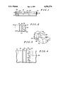
- FIG. 1 comprises a side elevational view of the invention
- FIG. 2 comprises a top plan view of the invention
- FIG. 3 comprises a perspective view of the invention
- FIG. 4 comprises a top plan view of an alternative embodiment of the invention.
- the device includes generally a substrate (101), a first electrode (102), a second electrode (103), a third electrode (104), and a fourth electrode (110).
- the substrate should generally be comprised of an insulator (a conductor may be used, but the upper surface of the conductor should be coated with an insulating layer).
- the first electrode (102), in this embodiment, comprises an emitter.
- multiple layers of insulating material (106) in this case silicon dioxide
- the conductive layer (107) comprising the first electrode (102) has a pointed portion (108). This wedge shaped portion functions, when the device is operational, to source electrons as explained in more detail below.
- the second electrode (103) forms a gate and is formed by successive depositions of conductive material. Importantly, as visible in FIG. 2, the second electrode (103) includes a notch (109) formed therein for receiving the pointed end (108) of the first electrode (102). The purpose of this configuration will be made more clear below.
- the third electrode (104) comprises a first collector and is formed by successive depositions of conductive material (111) on the surface of the substrate (101). With reference to FIG. 3, it can be more clearly seen that the pointed tip (108) of the first electrode (102) is disposed within the notch area (109) formed in the gate (103). At the same time, the insulator (106) and the air gap ensures that the first electrode (102) does not contact the gate (103).
- the fourth electrode (110) comprises a second collector and is formed by deposition of conductive material within a notch formed in the substrate (101). (This notch can either be formed through an etching process, or the conductive material can be added during a substrate building material deposition process.)
- appropriate field induced electron emission can be selectively achieved in at least two modes of operation.
- the required field is applied as a voltage to the gate (103) that is in sufficiently close proximity to the emitter (102) to induce electron emission.
- the emitted electrons are then transported from the emitter (102) to one of the collectors (104 and 110) in vacuum or atmosphere, as appropriate to the application.
- the dominant collector will be determined as a function primarily of the voltage applied thereto. In general, a somewhat stronger potential needs to be applied to the first collector (104) to compensate for the distance between the first collector (104) and the emitter (102). Conversely, a lesser voltage is required for the second collector (110) to achieve the same result.
- Energization, and off-device coupling, of the two collectors (anodes) can be selected as appropriate to a particular application.
- each device is formed substantially as described above, with the process replicated numerous times to achieve multiple parallel connected devices.
Abstract
A field emission device wherein two collecting electrodes are provided to selectively collect electrons that are emitted from an emitting electrode as induced by a gate electrode.
Description
This invention relates generally to field emission devices.
Field emission devices are known in the art. Such prior art devices are constructed in a vertical profile by means of complex deposition, etching, and evaporative metalization processes. Since the device elements are overlayed, the inter-element capacitances become significant and affect the performance of the device.
Typically, such prior art devices include a cathode, a gate to aid in controlling the emissions of the cathode, and an anode. Provision of only these three electrodes will not allow the resultant device to satisfactorily meet certain application needs.
There therefore exists a need for a field emission device that can be constructed in a simpler manner, that minimizes inter-element capacitance, and that meets applications needs not currently satisfied.
These needs and other needs are substantially met through provision of the planar field emission device disclosed herein. According to the invention, three electrodes of the device are disposed substantially coplanar with respect to one another, and not vertically. As a result, the device can be constructed in a simpler manner, and inter-element capacitance is minimized due to the improved proximity of the electrodes to a support surface. In addition, in one embodiment, the device includes a fourth electrode, which serves as a secondary anode. Electrons emitted by the cathode are collected by whichever of the two anodes are selectively engaged.
FIG. 1 comprises a side elevational view of the invention;
FIG. 2 comprises a top plan view of the invention;
FIG. 3 comprises a perspective view of the invention; and
FIG. 4 comprises a top plan view of an alternative embodiment of the invention.
Referring to FIG. 1, the invention can be seen as depicted generally by the numeral 100. The device includes generally a substrate (101), a first electrode (102), a second electrode (103), a third electrode (104), and a fourth electrode (110). The substrate should generally be comprised of an insulator (a conductor may be used, but the upper surface of the conductor should be coated with an insulating layer). The first electrode (102), in this embodiment, comprises an emitter. To form the emitter, multiple layers of insulating material (106) (in this case silicon dioxide) are deposited on the substrate (101) and a conductive layer (107) deposited thereon. With momentary reference to FIG. 2, the conductive layer (107) comprising the first electrode (102) has a pointed portion (108). This wedge shaped portion functions, when the device is operational, to source electrons as explained in more detail below.
The second electrode (103) forms a gate and is formed by successive depositions of conductive material. Importantly, as visible in FIG. 2, the second electrode (103) includes a notch (109) formed therein for receiving the pointed end (108) of the first electrode (102). The purpose of this configuration will be made more clear below.
The third electrode (104) comprises a first collector and is formed by successive depositions of conductive material (111) on the surface of the substrate (101). With reference to FIG. 3, it can be more clearly seen that the pointed tip (108) of the first electrode (102) is disposed within the notch area (109) formed in the gate (103). At the same time, the insulator (106) and the air gap ensures that the first electrode (102) does not contact the gate (103).
Lastly, the fourth electrode (110) comprises a second collector and is formed by deposition of conductive material within a notch formed in the substrate (101). (This notch can either be formed through an etching process, or the conductive material can be added during a substrate building material deposition process.)
So configured, appropriate field induced electron emission can be selectively achieved in at least two modes of operation. The required field is applied as a voltage to the gate (103) that is in sufficiently close proximity to the emitter (102) to induce electron emission. The emitted electrons are then transported from the emitter (102) to one of the collectors (104 and 110) in vacuum or atmosphere, as appropriate to the application. The dominant collector will be determined as a function primarily of the voltage applied thereto. In general, a somewhat stronger potential needs to be applied to the first collector (104) to compensate for the distance between the first collector (104) and the emitter (102). Conversely, a lesser voltage is required for the second collector (110) to achieve the same result.
Energization, and off-device coupling, of the two collectors (anodes) can be selected as appropriate to a particular application.
Referring to FIG. 4, it can be seen that a plurality of such three electrode devices can be formed on a substrate (101) in a parallel manner, to achieve improved power capabilities. In this embodiment, each device is formed substantially as described above, with the process replicated numerous times to achieve multiple parallel connected devices.
Claims (5)
1. A field emission device, comprising:
(A) an emitter for emitting electrons;
(B) a first anode disposed substantially coplanar with respect to the emitter for collecting at least some of the electrons;
(C) a second anode for selectively collecting at least some of the electrons, such that when the second anode collects electrons, the first anode does not collect electrons.
2. The field emission device of claim 1, wherein the device further includes a gate that acts to induce electron emission from the emitter.
3. A field emission device, comprising:
(A) a substrate;
(B) emitter means formed on the substrate for emitting electrons;
(C) first anode means formed on the substrate and disposed substantially coplanar with respect to the emitter means for collecting at least some of the electrons;
(D) second anode means formed on the substrate for selectively collecting at least some of the electrons, such that when the second anode means collects electrons, the first anode means does not collect electrons.
4. The field emission device of claim 1, wherein the device further includes a gate that acts to induce electron emission from the emitter.
5. A method of forming a field emission device, comprising:
(A) providing a substrate;
(B) forming a first electrode on the substrate, which first electrode acts as an electron source;
(C) forming a second electrode on the substrate substantially co-planar with the first electrode, which second electrode acts to induce electron emission from the first electrode;
(D) forming a third electrode on the substrate substantially co-planar with the first electrode, which third electrode acts to collect at least some of the electrons sourced by the first electrode;
(E) forming a fourth electrode on the substrate, which fourth electrode acts to collect at least some of the electrons sourced by the first electrode, such that when the fourth electrode collects electrons, the third electrode does not collect electrons.
Priority Applications (7)
| Application Number | Priority Date | Filing Date | Title |
|---|---|---|---|
| US07/391,211 US4956574A (en) | 1989-08-08 | 1989-08-08 | Switched anode field emission device |
| AU59263/90A AU621001B2 (en) | 1989-08-08 | 1990-06-18 | Switched anode field emission device |
| JP2509887A JPH04502229A (en) | 1989-08-08 | 1990-06-18 | Switchable anode field emission device |
| EP90909883A EP0452425A1 (en) | 1989-08-08 | 1990-06-18 | Switched anode field emission device |
| PCT/US1990/003385 WO1991002371A1 (en) | 1989-08-08 | 1990-06-18 | Switched anode field emission device |
| HU8653A HUT57944A (en) | 1989-08-08 | 1990-06-18 | Field emission element of switched anode |
| BR909006876A BR9006876A (en) | 1989-08-08 | 1990-06-18 | FIELD EMISSION DEVICE AND PROCESS FOR ITS FORMATION |
Applications Claiming Priority (1)
| Application Number | Priority Date | Filing Date | Title |
|---|---|---|---|
| US07/391,211 US4956574A (en) | 1989-08-08 | 1989-08-08 | Switched anode field emission device |
Publications (1)
| Publication Number | Publication Date |
|---|---|
| US4956574A true US4956574A (en) | 1990-09-11 |
Family
ID=23545730
Family Applications (1)
| Application Number | Title | Priority Date | Filing Date |
|---|---|---|---|
| US07/391,211 Expired - Lifetime US4956574A (en) | 1989-08-08 | 1989-08-08 | Switched anode field emission device |
Country Status (7)
| Country | Link |
|---|---|
| US (1) | US4956574A (en) |
| EP (1) | EP0452425A1 (en) |
| JP (1) | JPH04502229A (en) |
| AU (1) | AU621001B2 (en) |
| BR (1) | BR9006876A (en) |
| HU (1) | HUT57944A (en) |
| WO (1) | WO1991002371A1 (en) |
Cited By (34)
| Publication number | Priority date | Publication date | Assignee | Title |
|---|---|---|---|---|
| WO1991005363A1 (en) * | 1989-09-29 | 1991-04-18 | Motorola, Inc. | Flat panel display using field emission devices |
| WO1991012625A1 (en) * | 1990-02-09 | 1991-08-22 | Motorola, Inc. | Encapsulated field emission device |
| US5053673A (en) * | 1988-10-17 | 1991-10-01 | Matsushita Electric Industrial Co., Ltd. | Field emission cathodes and method of manufacture thereof |
| DE4132150A1 (en) * | 1990-09-27 | 1992-04-02 | Futaba Denshi Kogyo Kk | FIELD EMISSION ELEMENT AND METHOD FOR THE PRODUCTION THEREOF |
| JPH0474834U (en) * | 1990-11-08 | 1992-06-30 | ||
| US5136764A (en) * | 1990-09-27 | 1992-08-11 | Motorola, Inc. | Method for forming a field emission device |
| EP0498254A1 (en) * | 1991-01-28 | 1992-08-12 | Sony Corporation | Microelectronic ballistic transistor and process of manufacturing the same |
| US5144191A (en) * | 1991-06-12 | 1992-09-01 | Mcnc | Horizontal microelectronic field emission devices |
| FR2673481A1 (en) * | 1991-02-28 | 1992-09-04 | Motorola Inc | FIELD EMISSION TYPE DISPLAY UNIT, USING A FLAT FIELD EMISSION DEVICE AS A CONTROL DEVICE. |
| US5173634A (en) * | 1990-11-30 | 1992-12-22 | Motorola, Inc. | Current regulated field-emission device |
| US5220725A (en) * | 1991-04-09 | 1993-06-22 | Northeastern University | Micro-emitter-based low-contact-force interconnection device |
| US5245248A (en) * | 1991-04-09 | 1993-09-14 | Northeastern University | Micro-emitter-based low-contact-force interconnection device |
| US5272411A (en) * | 1992-01-28 | 1993-12-21 | Itt Corporation | Coaxial triode apparatus |
| US5312777A (en) * | 1992-09-25 | 1994-05-17 | International Business Machines Corporation | Fabrication methods for bidirectional field emission devices and storage structures |
| US5359256A (en) * | 1992-07-30 | 1994-10-25 | The United States Of America As Represented By The Secretary Of The Navy | Regulatable field emitter device and method of production thereof |
| US5382867A (en) * | 1991-10-02 | 1995-01-17 | Sharp Kabushiki Kaisha | Field-emission type electronic device |
| US5384509A (en) * | 1991-07-18 | 1995-01-24 | Motorola, Inc. | Field emission device with horizontal emitter |
| US5424605A (en) * | 1992-04-10 | 1995-06-13 | Silicon Video Corporation | Self supporting flat video display |
| US5445550A (en) * | 1993-12-22 | 1995-08-29 | Xie; Chenggang | Lateral field emitter device and method of manufacturing same |
| US5477105A (en) * | 1992-04-10 | 1995-12-19 | Silicon Video Corporation | Structure of light-emitting device with raised black matrix for use in optical devices such as flat-panel cathode-ray tubes |
| US5601966A (en) * | 1993-11-04 | 1997-02-11 | Microelectronics And Computer Technology Corporation | Methods for fabricating flat panel display systems and components |
| US5660570A (en) * | 1991-04-09 | 1997-08-26 | Northeastern University | Micro emitter based low contact force interconnection device |
| US5675216A (en) * | 1992-03-16 | 1997-10-07 | Microelectronics And Computer Technololgy Corp. | Amorphic diamond film flat field emission cathode |
| US5686790A (en) * | 1993-06-22 | 1997-11-11 | Candescent Technologies Corporation | Flat panel device with ceramic backplate |
| US5703435A (en) * | 1992-03-16 | 1997-12-30 | Microelectronics & Computer Technology Corp. | Diamond film flat field emission cathode |
| US5965971A (en) * | 1993-01-19 | 1999-10-12 | Kypwee Display Corporation | Edge emitter display device |
| US6011567A (en) * | 1990-12-28 | 2000-01-04 | Canon Kabushiki Kaisha | Image forming apparatus |
| US6127773A (en) * | 1992-03-16 | 2000-10-03 | Si Diamond Technology, Inc. | Amorphic diamond film flat field emission cathode |
| US6629869B1 (en) | 1992-03-16 | 2003-10-07 | Si Diamond Technology, Inc. | Method of making flat panel displays having diamond thin film cathode |
| US20050017648A1 (en) * | 2003-07-22 | 2005-01-27 | Ron Naaman | Display device |
| US6909104B1 (en) * | 1999-05-25 | 2005-06-21 | Nawotec Gmbh | Miniaturized terahertz radiation source |
| US20070049731A1 (en) * | 2002-06-26 | 2007-03-01 | Kevin Thorne | Rapid Isolation of Osteoinductive Protein Mixtures from Mammalian Bone Tissue |
| US20090244398A1 (en) * | 2004-05-18 | 2009-10-01 | Canon Kabushiki Kaisha | Electron-emitting device, electron-emitting apparatus, electron source, image display device and information display/reproduction apparatus |
| US20200219693A1 (en) * | 2018-08-30 | 2020-07-09 | The Institute of Microelectronics of Chinese Academy of Sciences | Field emission cathode electron source and array thereof |
Families Citing this family (1)
| Publication number | Priority date | Publication date | Assignee | Title |
|---|---|---|---|---|
| JP3235172B2 (en) * | 1991-05-13 | 2001-12-04 | セイコーエプソン株式会社 | Field electron emission device |
Citations (20)
| Publication number | Priority date | Publication date | Assignee | Title |
|---|---|---|---|---|
| US3755704A (en) * | 1970-02-06 | 1973-08-28 | Stanford Research Inst | Field emission cathode structures and devices utilizing such structures |
| US3789471A (en) * | 1970-02-06 | 1974-02-05 | Stanford Research Inst | Field emission cathode structures, devices utilizing such structures, and methods of producing such structures |
| US3812559A (en) * | 1970-07-13 | 1974-05-28 | Stanford Research Inst | Methods of producing field ionizer and field emission cathode structures |
| US3894332A (en) * | 1972-02-11 | 1975-07-15 | Westinghouse Electric Corp | Solid state radiation sensitive field electron emitter and methods of fabrication thereof |
| US3921022A (en) * | 1974-09-03 | 1975-11-18 | Rca Corp | Field emitting device and method of making same |
| US3970887A (en) * | 1974-06-19 | 1976-07-20 | Micro-Bit Corporation | Micro-structure field emission electron source |
| US3998678A (en) * | 1973-03-22 | 1976-12-21 | Hitachi, Ltd. | Method of manufacturing thin-film field-emission electron source |
| US4008412A (en) * | 1974-08-16 | 1977-02-15 | Hitachi, Ltd. | Thin-film field-emission electron source and a method for manufacturing the same |
| US4178531A (en) * | 1977-06-15 | 1979-12-11 | Rca Corporation | CRT with field-emission cathode |
| SU855782A1 (en) * | 1977-06-28 | 1981-08-15 | Предприятие П/Я Г-4468 | Electron emitter |
| US4307507A (en) * | 1980-09-10 | 1981-12-29 | The United States Of America As Represented By The Secretary Of The Navy | Method of manufacturing a field-emission cathode structure |
| US4513308A (en) * | 1982-09-23 | 1985-04-23 | The United States Of America As Represented By The Secretary Of The Navy | p-n Junction controlled field emitter array cathode |
| EP0172089A1 (en) * | 1984-07-27 | 1986-02-19 | Commissariat à l'Energie Atomique | Display device using field emission excited cathode luminescence |
| US4578614A (en) * | 1982-07-23 | 1986-03-25 | The United States Of America As Represented By The Secretary Of The Navy | Ultra-fast field emitter array vacuum integrated circuit switching device |
| US4685996A (en) * | 1986-10-14 | 1987-08-11 | Busta Heinz H | Method of making micromachined refractory metal field emitters |
| US4721885A (en) * | 1987-02-11 | 1988-01-26 | Sri International | Very high speed integrated microelectronic tubes |
| FR2604823A1 (en) * | 1986-10-02 | 1988-04-08 | Etude Surfaces Lab | ELECTRON EMITTING DEVICE AND ITS APPLICATION IN PARTICULAR TO THE PRODUCTION OF TELEVISION DISPLAY SCREENS |
| GB2204991A (en) * | 1987-05-18 | 1988-11-23 | Gen Electric Plc | Vacuum electronic device |
| US4827177A (en) * | 1986-09-08 | 1989-05-02 | The General Electric Company, P.L.C. | Field emission vacuum devices |
| US4874981A (en) * | 1988-05-10 | 1989-10-17 | Sri International | Automatically focusing field emission electrode |
Family Cites Families (5)
| Publication number | Priority date | Publication date | Assignee | Title |
|---|---|---|---|---|
| US4728851A (en) * | 1982-01-08 | 1988-03-01 | Ford Motor Company | Field emitter device with gated memory |
| US4663559A (en) * | 1982-09-17 | 1987-05-05 | Christensen Alton O | Field emission device |
| US4904895A (en) * | 1987-05-06 | 1990-02-27 | Canon Kabushiki Kaisha | Electron emission device |
| US4855636A (en) * | 1987-10-08 | 1989-08-08 | Busta Heinz H | Micromachined cold cathode vacuum tube device and method of making |
| FR2623013A1 (en) * | 1987-11-06 | 1989-05-12 | Commissariat Energie Atomique | ELECTRO SOURCE WITH EMISSIVE MICROPOINT CATHODES AND FIELD EMISSION-INDUCED CATHODOLUMINESCENCE VISUALIZATION DEVICE USING THE SOURCE |
-
1989
- 1989-08-08 US US07/391,211 patent/US4956574A/en not_active Expired - Lifetime
-
1990
- 1990-06-18 EP EP90909883A patent/EP0452425A1/en not_active Withdrawn
- 1990-06-18 WO PCT/US1990/003385 patent/WO1991002371A1/en not_active Application Discontinuation
- 1990-06-18 HU HU8653A patent/HUT57944A/en unknown
- 1990-06-18 JP JP2509887A patent/JPH04502229A/en active Pending
- 1990-06-18 BR BR909006876A patent/BR9006876A/en not_active Application Discontinuation
- 1990-06-18 AU AU59263/90A patent/AU621001B2/en not_active Ceased
Patent Citations (20)
| Publication number | Priority date | Publication date | Assignee | Title |
|---|---|---|---|---|
| US3755704A (en) * | 1970-02-06 | 1973-08-28 | Stanford Research Inst | Field emission cathode structures and devices utilizing such structures |
| US3789471A (en) * | 1970-02-06 | 1974-02-05 | Stanford Research Inst | Field emission cathode structures, devices utilizing such structures, and methods of producing such structures |
| US3812559A (en) * | 1970-07-13 | 1974-05-28 | Stanford Research Inst | Methods of producing field ionizer and field emission cathode structures |
| US3894332A (en) * | 1972-02-11 | 1975-07-15 | Westinghouse Electric Corp | Solid state radiation sensitive field electron emitter and methods of fabrication thereof |
| US3998678A (en) * | 1973-03-22 | 1976-12-21 | Hitachi, Ltd. | Method of manufacturing thin-film field-emission electron source |
| US3970887A (en) * | 1974-06-19 | 1976-07-20 | Micro-Bit Corporation | Micro-structure field emission electron source |
| US4008412A (en) * | 1974-08-16 | 1977-02-15 | Hitachi, Ltd. | Thin-film field-emission electron source and a method for manufacturing the same |
| US3921022A (en) * | 1974-09-03 | 1975-11-18 | Rca Corp | Field emitting device and method of making same |
| US4178531A (en) * | 1977-06-15 | 1979-12-11 | Rca Corporation | CRT with field-emission cathode |
| SU855782A1 (en) * | 1977-06-28 | 1981-08-15 | Предприятие П/Я Г-4468 | Electron emitter |
| US4307507A (en) * | 1980-09-10 | 1981-12-29 | The United States Of America As Represented By The Secretary Of The Navy | Method of manufacturing a field-emission cathode structure |
| US4578614A (en) * | 1982-07-23 | 1986-03-25 | The United States Of America As Represented By The Secretary Of The Navy | Ultra-fast field emitter array vacuum integrated circuit switching device |
| US4513308A (en) * | 1982-09-23 | 1985-04-23 | The United States Of America As Represented By The Secretary Of The Navy | p-n Junction controlled field emitter array cathode |
| EP0172089A1 (en) * | 1984-07-27 | 1986-02-19 | Commissariat à l'Energie Atomique | Display device using field emission excited cathode luminescence |
| US4827177A (en) * | 1986-09-08 | 1989-05-02 | The General Electric Company, P.L.C. | Field emission vacuum devices |
| FR2604823A1 (en) * | 1986-10-02 | 1988-04-08 | Etude Surfaces Lab | ELECTRON EMITTING DEVICE AND ITS APPLICATION IN PARTICULAR TO THE PRODUCTION OF TELEVISION DISPLAY SCREENS |
| US4685996A (en) * | 1986-10-14 | 1987-08-11 | Busta Heinz H | Method of making micromachined refractory metal field emitters |
| US4721885A (en) * | 1987-02-11 | 1988-01-26 | Sri International | Very high speed integrated microelectronic tubes |
| GB2204991A (en) * | 1987-05-18 | 1988-11-23 | Gen Electric Plc | Vacuum electronic device |
| US4874981A (en) * | 1988-05-10 | 1989-10-17 | Sri International | Automatically focusing field emission electrode |
Non-Patent Citations (8)
| Title |
|---|
| A Vacuum Field Effect Transistor Using Silicon Field Emitter Arrays, by Gary, 12/86 IEDM 86, pp. 776 779. * |
| A Vacuum Field Effect Transistor Using Silicon Field Emitter Arrays, by Gary, 12/86 IEDM 86, pp. 776-779. |
| Advanced Technology: Flat Cold Cathode CRTs, by Ivor Brodie, Information Display, 1/89, pp. 17 19. * |
| Advanced Technology: Flat Cold-Cathode CRTs, by Ivor Brodie, Information Display, 1/89, pp. 17-19. |
| Field Emission Cathode Array Development for High Current Density Applications by Spindt et al., dated Aug., 1982, vol. 16, of Applications of Surface Science, pp. 268 276. * |
| Field Emission Cathode Array Development for High-Current Density Applications by Spindt et al., dated Aug., 1982, vol. 16, of Applications of Surface Science, pp. 268-276. |
| Field Emitter Arrays Applied to Vacuum Flourescent Display, by Spindt et al., Jan., 1989, issue of IEEE Transactions on Electronic Devices, pp. 225 228. * |
| Field-Emitter Arrays Applied to Vacuum Flourescent Display, by Spindt et al., Jan., 1989, issue of IEEE Transactions on Electronic Devices, pp. 225-228. |
Cited By (58)
| Publication number | Priority date | Publication date | Assignee | Title |
|---|---|---|---|---|
| US5053673A (en) * | 1988-10-17 | 1991-10-01 | Matsushita Electric Industrial Co., Ltd. | Field emission cathodes and method of manufacture thereof |
| US5465024A (en) * | 1989-09-29 | 1995-11-07 | Motorola, Inc. | Flat panel display using field emission devices |
| WO1991005363A1 (en) * | 1989-09-29 | 1991-04-18 | Motorola, Inc. | Flat panel display using field emission devices |
| WO1991012625A1 (en) * | 1990-02-09 | 1991-08-22 | Motorola, Inc. | Encapsulated field emission device |
| US5079476A (en) * | 1990-02-09 | 1992-01-07 | Motorola, Inc. | Encapsulated field emission device |
| US5136764A (en) * | 1990-09-27 | 1992-08-11 | Motorola, Inc. | Method for forming a field emission device |
| DE4132150C2 (en) * | 1990-09-27 | 2002-01-10 | Futaba Denshi Kogyo Kk | Field emission element and method for its production |
| DE4132150A1 (en) * | 1990-09-27 | 1992-04-02 | Futaba Denshi Kogyo Kk | FIELD EMISSION ELEMENT AND METHOD FOR THE PRODUCTION THEREOF |
| JP2562168Y2 (en) | 1990-11-08 | 1998-02-10 | 双葉電子工業株式会社 | Field emission device |
| JPH0474834U (en) * | 1990-11-08 | 1992-06-30 | ||
| US5173634A (en) * | 1990-11-30 | 1992-12-22 | Motorola, Inc. | Current regulated field-emission device |
| US6011567A (en) * | 1990-12-28 | 2000-01-04 | Canon Kabushiki Kaisha | Image forming apparatus |
| EP0498254A1 (en) * | 1991-01-28 | 1992-08-12 | Sony Corporation | Microelectronic ballistic transistor and process of manufacturing the same |
| US5289077A (en) * | 1991-01-28 | 1994-02-22 | Sony Corporation | Microelectronic ballistic transistor |
| FR2673481A1 (en) * | 1991-02-28 | 1992-09-04 | Motorola Inc | FIELD EMISSION TYPE DISPLAY UNIT, USING A FLAT FIELD EMISSION DEVICE AS A CONTROL DEVICE. |
| US5245248A (en) * | 1991-04-09 | 1993-09-14 | Northeastern University | Micro-emitter-based low-contact-force interconnection device |
| US5220725A (en) * | 1991-04-09 | 1993-06-22 | Northeastern University | Micro-emitter-based low-contact-force interconnection device |
| US5660570A (en) * | 1991-04-09 | 1997-08-26 | Northeastern University | Micro emitter based low contact force interconnection device |
| US5144191A (en) * | 1991-06-12 | 1992-09-01 | Mcnc | Horizontal microelectronic field emission devices |
| US5384509A (en) * | 1991-07-18 | 1995-01-24 | Motorola, Inc. | Field emission device with horizontal emitter |
| US5382867A (en) * | 1991-10-02 | 1995-01-17 | Sharp Kabushiki Kaisha | Field-emission type electronic device |
| US5272411A (en) * | 1992-01-28 | 1993-12-21 | Itt Corporation | Coaxial triode apparatus |
| US6629869B1 (en) | 1992-03-16 | 2003-10-07 | Si Diamond Technology, Inc. | Method of making flat panel displays having diamond thin film cathode |
| US6127773A (en) * | 1992-03-16 | 2000-10-03 | Si Diamond Technology, Inc. | Amorphic diamond film flat field emission cathode |
| US5703435A (en) * | 1992-03-16 | 1997-12-30 | Microelectronics & Computer Technology Corp. | Diamond film flat field emission cathode |
| US5675216A (en) * | 1992-03-16 | 1997-10-07 | Microelectronics And Computer Technololgy Corp. | Amorphic diamond film flat field emission cathode |
| US5597518A (en) * | 1992-04-10 | 1997-01-28 | Silicon Video Corporation | Method for producing self supporting flat video display |
| US5725787A (en) * | 1992-04-10 | 1998-03-10 | Candescent Technologies Corporation | Fabrication of light-emitting device with raised black matrix for use in optical devices such as flat-panel cathode-ray tubes |
| US5576596A (en) * | 1992-04-10 | 1996-11-19 | Silicon Video Corporation | Optical devices such as flat-panel cathode ray tube, having raised black matrix |
| US5424605A (en) * | 1992-04-10 | 1995-06-13 | Silicon Video Corporation | Self supporting flat video display |
| US5541473A (en) * | 1992-04-10 | 1996-07-30 | Silicon Video Corporation | Grid addressed field emission cathode |
| US5667418A (en) * | 1992-04-10 | 1997-09-16 | Candescent Technologies Corporation | Method of fabricating flat panel device having internal support structure |
| US5674351A (en) * | 1992-04-10 | 1997-10-07 | Candescent Technologies Corporation | Self supporting flat video display |
| US5589731A (en) * | 1992-04-10 | 1996-12-31 | Silicon Video Corporation | Internal support structure for flat panel device |
| US5798604A (en) * | 1992-04-10 | 1998-08-25 | Candescent Technologies Corporation | Flat panel display with gate layer in contact with thicker patterned further conductive layer |
| US5477105A (en) * | 1992-04-10 | 1995-12-19 | Silicon Video Corporation | Structure of light-emitting device with raised black matrix for use in optical devices such as flat-panel cathode-ray tubes |
| US5359256A (en) * | 1992-07-30 | 1994-10-25 | The United States Of America As Represented By The Secretary Of The Navy | Regulatable field emitter device and method of production thereof |
| US5312777A (en) * | 1992-09-25 | 1994-05-17 | International Business Machines Corporation | Fabrication methods for bidirectional field emission devices and storage structures |
| US5530262A (en) * | 1992-09-25 | 1996-06-25 | International Business Machines Corporation | Bidirectional field emission devices, storage structures and fabrication methods |
| US5965971A (en) * | 1993-01-19 | 1999-10-12 | Kypwee Display Corporation | Edge emitter display device |
| US6023126A (en) * | 1993-01-19 | 2000-02-08 | Kypwee Display Corporation | Edge emitter with secondary emission display |
| US5686790A (en) * | 1993-06-22 | 1997-11-11 | Candescent Technologies Corporation | Flat panel device with ceramic backplate |
| US5652083A (en) * | 1993-11-04 | 1997-07-29 | Microelectronics And Computer Technology Corporation | Methods for fabricating flat panel display systems and components |
| US5614353A (en) * | 1993-11-04 | 1997-03-25 | Si Diamond Technology, Inc. | Methods for fabricating flat panel display systems and components |
| US5601966A (en) * | 1993-11-04 | 1997-02-11 | Microelectronics And Computer Technology Corporation | Methods for fabricating flat panel display systems and components |
| US5445550A (en) * | 1993-12-22 | 1995-08-29 | Xie; Chenggang | Lateral field emitter device and method of manufacturing same |
| US5528099A (en) * | 1993-12-22 | 1996-06-18 | Microelectronics And Computer Technology Corporation | Lateral field emitter device |
| US6909104B1 (en) * | 1999-05-25 | 2005-06-21 | Nawotec Gmbh | Miniaturized terahertz radiation source |
| US20070049731A1 (en) * | 2002-06-26 | 2007-03-01 | Kevin Thorne | Rapid Isolation of Osteoinductive Protein Mixtures from Mammalian Bone Tissue |
| WO2005008711A2 (en) * | 2003-07-22 | 2005-01-27 | Yeda Research And Development Company Ltd. | Electron emission device |
| US20050018467A1 (en) * | 2003-07-22 | 2005-01-27 | Ron Naaman | Electron emission device |
| WO2005008711A3 (en) * | 2003-07-22 | 2005-08-11 | Yeda Res & Dev | Electron emission device |
| US20050017648A1 (en) * | 2003-07-22 | 2005-01-27 | Ron Naaman | Display device |
| US7646149B2 (en) | 2003-07-22 | 2010-01-12 | Yeda Research and Development Company, Ltd, | Electronic switching device |
| US20090244398A1 (en) * | 2004-05-18 | 2009-10-01 | Canon Kabushiki Kaisha | Electron-emitting device, electron-emitting apparatus, electron source, image display device and information display/reproduction apparatus |
| US8022608B2 (en) * | 2004-05-18 | 2011-09-20 | Canon Kabushiki Kaisha | Electron-emitting device, electron-emitting apparatus, electron source, image display device and information display/reproduction apparatus |
| US20200219693A1 (en) * | 2018-08-30 | 2020-07-09 | The Institute of Microelectronics of Chinese Academy of Sciences | Field emission cathode electron source and array thereof |
| US10840050B2 (en) * | 2018-08-30 | 2020-11-17 | The Institute of Microelectronics of Chinese Academy of Sciences | Field emission cathode electron source and array thereof |
Also Published As
| Publication number | Publication date |
|---|---|
| EP0452425A1 (en) | 1991-10-23 |
| JPH04502229A (en) | 1992-04-16 |
| WO1991002371A1 (en) | 1991-02-21 |
| AU621001B2 (en) | 1992-02-27 |
| HUT57944A (en) | 1991-12-30 |
| AU5926390A (en) | 1991-03-11 |
| EP0452425A4 (en) | 1991-07-24 |
| HU905386D0 (en) | 1991-07-29 |
| BR9006876A (en) | 1991-08-27 |
Similar Documents
| Publication | Publication Date | Title |
|---|---|---|
| US4956574A (en) | Switched anode field emission device | |
| US5666019A (en) | High-frequency field-emission device | |
| EP0306173B1 (en) | Field emission devices | |
| US5075595A (en) | Field emission device with vertically integrated active control | |
| US7504767B2 (en) | Electrode structures, display devices containing the same | |
| US5173634A (en) | Current regulated field-emission device | |
| US5281890A (en) | Field emission device having a central anode | |
| US6899584B2 (en) | Insulated gate field emitter array | |
| KR960019421A (en) | Electron Emission Device and Manufacturing Method Thereof | |
| US5181874A (en) | Method of making microelectronic field emission device with air bridge anode | |
| JPH0340332A (en) | Electric field emitting type switching element and manufacture thereof | |
| US5136205A (en) | Microelectronic field emission device with air bridge anode | |
| US5430348A (en) | Inversion mode diamond electron source | |
| US5628663A (en) | Fabrication process for high-frequency field-emission device | |
| US5631196A (en) | Method for making inversion mode diamond electron source | |
| US20050275336A1 (en) | Field emission device and method for making same | |
| JP3010304B2 (en) | Vacuum tube | |
| CA2085982A1 (en) | Structures and processes for fabricating field emission cathodes | |
| JP2763219B2 (en) | Field emission type electronic device | |
| WO1997009733A1 (en) | High-frequency field-emission device and fabrication process | |
| KR960014805B1 (en) | Vmd structure and manufacturing method | |
| JPH0567426A (en) | Electric field emission type electron source | |
| JP2900692B2 (en) | Vacuum micro amplification device | |
| CN115498025A (en) | Vertical nano air channel triode with grid electrode protection layer and preparation method thereof | |
| WO1998054745B1 (en) | Structure and fabrication of electron-emitting device having specially configured focus coating |
Legal Events
| Date | Code | Title | Description |
|---|---|---|---|
| AS | Assignment |
Owner name: MOTOROLA, INC., SCHAUMBURG, IL A CORP. OF DELAWARE Free format text: ASSIGNMENT OF ASSIGNORS INTEREST.;ASSIGNOR:KANE, ROBERT C.;REEL/FRAME:005111/0442 Effective date: 19890808 |
|
| STCF | Information on status: patent grant |
Free format text: PATENTED CASE |
|
| FPAY | Fee payment |
Year of fee payment: 4 |
|
| FPAY | Fee payment |
Year of fee payment: 8 |
|
| FPAY | Fee payment |
Year of fee payment: 12 |
|
| REMI | Maintenance fee reminder mailed |