US4943909A - Computational origami - Google Patents
Computational origami Download PDFInfo
- Publication number
- US4943909A US4943909A US07/071,105 US7110587A US4943909A US 4943909 A US4943909 A US 4943909A US 7110587 A US7110587 A US 7110587A US 4943909 A US4943909 A US 4943909A
- Authority
- US
- United States
- Prior art keywords
- processing
- row
- processing element
- output
- column
- Prior art date
- Legal status (The legal status is an assumption and is not a legal conclusion. Google has not performed a legal analysis and makes no representation as to the accuracy of the status listed.)
- Expired - Lifetime
Links
Images


Classifications
-
- G—PHYSICS
- G06—COMPUTING; CALCULATING OR COUNTING
- G06F—ELECTRIC DIGITAL DATA PROCESSING
- G06F15/00—Digital computers in general; Data processing equipment in general
- G06F15/76—Architectures of general purpose stored program computers
- G06F15/80—Architectures of general purpose stored program computers comprising an array of processing units with common control, e.g. single instruction multiple data processors
- G06F15/8007—Architectures of general purpose stored program computers comprising an array of processing units with common control, e.g. single instruction multiple data processors single instruction multiple data [SIMD] multiprocessors
- G06F15/8023—Two dimensional arrays, e.g. mesh, torus
Definitions
- This invention relates to parallel computing, and more specifically to the art of processor architectures that are suitable for highly parallel computations.
- the major issues in parallel computing is identifying a sufficient parallelism to exploit, synchronizing the various processors, and managing the communications between the processing units.
- Multiprocessor networds are another type of parallel computer architectures.
- several computers work concurrently on different discernible portions of a problem, and communicate with each other via messages through the interconnection network to communicate intermediate results and to coordinate the overall solution.
- the granularity of the parallelism in multiprocessor networks is typically very coarse.
- a problem is divided into major divisible portions and each processor operates independently until the solution to the divisible portion is developed.
- the division lines of the problem are selected to minimize the necessary communications and coordination, since the communications process is cumbersome, requiring "handshaking" protocols.
- This architecture is usually employed with problems that have a high degree of parallelism, relatively simple coordination, and relatively little communication. The reason for that lies in the fact that dividing the problem into subparts often introduces a large communications and coordination burden that overloads the architecture.
- the "Hypercube" as implemented in Cal Tech by [reference] is an example of such a computer network architecture.
- Data flow architecture from yet another type of parallel computer architectures This architecture is employed most often when the algorithm to be executed can be decomposed into several portions which can be processed independently.
- This architecture is characterized by a plurality of processors to which the algorithm portions are assigned, and each processor is activated upon arrival of all of the required inputs. As a result, the coordination of the computations is acommplished by the flow of the data. It is quite a general approach for exploiting all of the parallelism that an algorithm has to offer. The main disadvantage is in managing communications to prevent interdependencies which would lead to a "deadlock" situation.
- Array processorsd comprise another type of parallel computer architecture.
- This architecture consists of many functionally equivalent processing elements (PEs) that operate under control of a single control unit.
- PEs processing elements
- the various processing elements are interconnected to permit data to flow between the processing elements.
- the interconnection topologies are fixed, although different designs employ different topologies. Some of the interconnection topologies are described in articles such as "Data Manipulating Functions in Parallel Processors and Their Implementation" T. Feng, IEEE Transactions on Computers, Vol. C-23, Number 3, Mar. 1974, pp. 309-318, "Access and Alignment of Data in an Array Processor" D. H. Lawrie, IEEE Transactions on Computers, Vol. C-24, Number 12, Mar. 1975, pp.
- array processors are most useful in applications where the same oepration is performed on many data items, such as in applications that involve matrix operations.
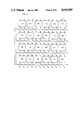
- FIG. 1 depicts a two dimensional rectangular array of processing elements
- FIG. 2 is the array of FIG. 1, functionally folded onto a single row of processing elements
- FIG. 3 is a two dimensional rectangular array where the processing elements in a row have no data dependencies on other processing elements in the row;
- FIG. 4 is a schematic diagram of a processing element that is useful in realizing the FIG. 3 arrangement
- FIG. 5 shows an arrangement with a single processing element combined with FIFO memory means and adapted to emulate an entire array of processing elements
- FIG. 6 illustrates the array connectivity that results from multiplexing the FIG. 5 arrangement to emulate an entire array
- FIGS. 7, 8 and 9 illustrate different processing array arrangements
- FIG. 10 presents an illustrative arrangement where the delay values are controllable
- FIG. 11 shows the interconnection flexibility within a processing array
- FIG. 12 is a schematic diagram of an example that is presented to illustrate the manner of implementing an arbitrary function
- FIGS. 13 and 14 show a mapping of the FIG. 12 example onto an array
- FIG. 15 depicts the realization of the FIG. 14 array with a multiplexed processing array of the type depicted in FIG. 7;
- FIG. 16 is a state diagram of another example that is presented to illustrate the manner of employing the principles of this invention.
- FIG. 17 presents a programmable logic array realization of the FIG. 16 state diagram, which assists in mapping the state diagram onto a regular array that is realizable in accordance with the principles of this invention
- FIG. 18 illustrates the arrangement for adding two numbers in a computational origami where the processing elements are half adders
- FIG. 19 depicts one means for realizing a half adder with an elemental processing elements of the type depicted in FIG. 5;
- FIG. 20 illustrates a cascaded arrangement
- the architecture of my invention overcomes many of the problems in the prior art architectures by employing a processing array of a few as a single processing element (with attendant memory) that emulates an entire array of processing elements.
- the emulated array may be arbitrarily large.
- My architecture differs from array processors in that large arrays (rows and columns) of processing elements are emulated with smaller arrays through the use of closely coupled delay elements and in that the processing elements also include a routing, or switching, capability. Control of the delay (and thus memory) in the delay elements determines the interconnection between the processing elements in the array, and full functionality is realized by allowing each processing element it the emulated array to perform any selected function without dependence on the function performed by the neighboring processing element.
- an algorithm to be implemented is conceptually mapped onto an array of processing elements arranged in rows and columns, where the data dependencies in the columns are unidirectional, and the data dependencies in the rows of processing elements are at most unidirectional.
- the scheduling of the processing and communications functions performed by the processing element is dictated by the conceptual array layout of the algorithm.
- FIG. 1 presents a two dimensional rectangular architecture which is illustrated in the aforementioned C. Mead et al. book at pp. 271-273. Its architecture is characterized by a rectangular interconnection of elemental processing units 10. Units 10-1 through 10-3 are shown in the first row, units 10-4 through 10-7 are shown in the second row, and unit 10-8 is shown in the last row.
- Each processor 10 in a particular column and row receives input signals from a processing element in the same column and in the previous row (e.g., via line 11 for unit 10-5) and from two adjacent processing elements in the same row and different columns--one from the left and one from the right--(e.g., lines 12 and 13 for unit 10-5).
- each element 10 provides output signals to the same adjacent processing elements in its row (e.g., lines 14 and 15 for unit 10-5) and to a processing element in its column and in the successive row (e.g., line 16 for unit 10-5).
- FIG. 1 architecture appears in the cited reference in connection with implementing of the so-called “inner product” operation in each processing element, it can be shown that the FIG. 1 architecture can be applied to perform any desired overall function by independently controlling the operation of each of the processing elements and enhancing the communications capability of the processing module to achieve a complete topological cover.
- This capability can be shown to exist from the following observation. Any task of processing can be divided into a collection of elemental processing steps responsive to input signals which can be carried out sequentially. Many of these processing steps can also be arranged for processing in parallel, followed by some sequentially arranged steps. Sequences of parallel execution of processing steps can be implemented with some general processing elements interconnected with some means for switching which directs the signals to the appropriate processing elements. With respect to FIG.
- steps to be performed in parallel can be assigned to a row of processors 10, subsequent steps to be performed in parallel can be assigned to a subsequent row of processing elements 10, and directing the signals to a subsequent row of processing elements 10 can be assigned to intervening row, or rows, of elements 10.
- Elements 10 can be used for switching because one can, in principle, communicate signals between columns, via the horizontal connections (lines 12, 13, 14, and 15). Additionally, it can be shown that the structure of FIG. 1 can realize all necessary computational and signal directing functions as long as each processing element 10 is capable of routing signals from any of the three inputs to any of three outputs, and performing at minimum the set of Boolean functions on the two input signals that form a complete Boolean cover.
- the first requirement relates to signal communication, while the second requirement relates to signal logical interactions. Together they permit computation.
- FIG. 1 In addition to realizing that the FIG. 1 architecture premits one to achieve any desired processing when the processing elements possess the above stated requirements, I have also realized that the computations in each row depend only on the results from the immediately previous row. What that means is that I can multiplex the operations performed in the various rows and fold them onto a single row of processors 17, as shown in FIG. 2.
- the only difference between processing elements 10 of FIG. 1 and processing elements 17 of FIG. 2 is that elements 17 must include some delay or latching means (delay line, flip-flop, register, or the like) to allow the results of one row's processing to feed back and affect the next row's processing.
- delay or latching means delay line, flip-flop, register, or the like
- FIG. 2 array It is realized, of course, that the overall processing throughout of the FIG. 2 array is reduced somewhat from the processing throughput of the FIG. 1 array. Some of the advantages of the FIG. 2 array are, however, that the hardware is minimized and the effective depth of the array (the effective number of rows) is variable and controllable, rather than fixed. The structure is, thus, decoupled from the particular algorithm that is being implemented.
- each of the processing elements in the row is controlled to perform a desired function independently of the function performed in any other processing element in the row (through function control bus 18). Further, none of the processing elements are "stuck" in time but, rather, each can perform different functions, when emulating different rows of the array.
- FIG. 2 architecture although very powerful, cannot be further reduced because each processing element 17 has data dependencies from both the left and the right adjacent processing elements in the row. That is, the processing of any element 17 cannot be completed until the processing in the adjacent elementon both sides is completed. One cannot, therefore, do the processing in a seriatim manner. This data dependence, or deadlock, prevents the computation from being futher decomposed and thus limits how much time can be traded off to reduce hardware.
- FIG. 3 architecture comprises processing elements 20 arranged in rows and columns, with each processing element 20 including two inputs and two outputs.
- the right input of each element 20 in FIG. 3 is derived from the left output in a processing element of the previous row and in the same column.
- the left input of each processing element is obtained from the right output in a processing element of the previous row and the left adjacent column.
- the adjacency relationship in each row is the same for all processing elements in the row.
- FIG. 4 depicts one embodiment for processing element 20.
- it is a very basic PLA which includes inputs 21 and 22 connected to a programmable three input by two output crossbar switch 23 which is used to distribute signals to output lines 26 and 27.
- Lines 21 and 22 are also combined in NOR gate 24, whose output is applied to crossbar switch 23.
- the cross points within crossbar switch 23 are controllable, or programmable, to effect particular interconnection patterns.
- Such controllable crosspoints may be realized with AND gates, as shown, that are controlled with a "customizing" control signal obtained from bus 30.
- element 20 can be as complex as practical, in the context of the desired functionality, operating speed (affecting throughput), and complexity of control. It can be, for example, a conventional CPU which is caused to execute any one of its rich set of primitive instructions, or even a complete computer which is caused to execute preselected subroutines.
- each processing element 17 must be used in conjunction with some delay or memory means.
- FIG. 4 processing element 20 is employed to realize the entire array of FIG. 3, different delay or memory means are necessary. This results from the fact that while the processing element implements the function of a particular element in a row, the values that were previously computed to the left of the particular element and in the same row, and to the right of the element and in the row above must be remembered.
- FIG. 5 depicts an arrangement for realizing the FIG. 3 architecture with a single processing element multiplexed to emulate both the rows and the columns. It includes a processing element 20 as described in FIG. 4 and, in addition, it includes OR gates 31 and 32 feeding element 20 and delay elements 33 and 34 (as discussed above) that receive input signals from the two output ports of element 20, respecitvely. More specifically, the right output of element 20 is applied to delay element 33, and the output of delay element 33 is connected to one of the inputs to OR gate 32. The output of OR gate 32 is connected to the left input of element 20. Correspondingly, the left output of element 20 is applied to delay element 34 and the output of delay element 34 is connected to one of the inputs of OR gate 31.
- Elements 33 and 34 are FIFO (first in, first out) memories and the delay provided by elements 33 and 34 is related, of course, to the "width" of the rows in the FIG. 3 architecture, i.e., to the number of processing elements in the rows of the emulated array. Specifically, the memory required of elements 33 and 34 is
- N is the "width" of the row.
- FIG. 3 circuit Since the FIG. 3 circuit is emulated with the FIG. 5 circuit through time multiplexing, the input, output, and control of the FIG. 5 circuit is sequential.
- the input signals are applied when the first row is emulated, and the output signals are extracted when the last row is emulated.
- the customizing control signals (bus 30) are applied with the emulation of each PE in the array. Also because of the time multiplexing, the inputs and the control signals must be applied repetitively, and the outputs must be repetitively captured. This aspect of my architecture is explained in more detail below in connection with an example.
- FIG. 5 circuit realizes an array architecture that is essentially identical to the one illustrated in FIG. 3; the only difference is in the treatment of signals at the array edges. That is, the FIG. 5 arrangement causes the array edge output signals to be naturally communicated as input signals at other array edge points and, although these connections are not always utilized, they contribute an additional degree of freedom in the implementation of a particular design.
- FIG. 6 illustrates the connectivity of the array edges (lines 41-44) when the FIG. 5 circuit is is used to emulate an entire array.
- the FIG. 5 arrangement includes a single processing element 20 which, in combination with the delay elements, emulates an entire array. Stated conversely, the entire array is folded into a single processing element.
- the degree of "folding" is selectable. It can be a function of the algorithm realized, the desired processing speed, the hardware available, or a combination of the above.
- FIGS. 7, 8 and 9 provide examples where the sub arrays employed comprise two processing elements in the same row, two processing elements in the same column, and a 2 ⁇ 2 array of processing elements.
- FIG. 7 employing two processing elements in a row requires the use of four delay elements, but each is about half the size of the delays in FIG. 5; to wit, one with a delay of N/2+1 (where N is the "length" of a row) and three with delays N/2.
- FIG. 8 employing two processing elements in a column requires the use of two delay elements as in FIG. 5 and, in addition, a delay element 35 of unit delay which connects the right most output of the top processing element (20-1) to the left most input of the lower processing element (20-2).
- FIG. 9 illustrates the case where an array is folded onto a 2 ⁇ 2 array of processing elements. It may be noted in passing that FIGS. 8-9 implement an array where the direction sense of column interconnections reverses from row to row.
- my architecture has the additional flexibility and advantage of concurrently (essentially) realizing any number of arrays of any size and in any order. That is, in one specific application there may be many inputs that appear concurrently and, therefore, it may be useful to have an array with long rows. Selecting the delay values (e.g., D 33 and D 34 ) appropriately provides the desired array width. In such an application the calculations may, perhaps, be accomplised very quickly so the required numbered of rows is small. In some other application, on the other hand, the row widths perhaps need not be large but the number of rows does need to be large. By the same technique of delay control the array may be modified to achieve that result.
- D 33 and D 34 selecting the delay values (e.g., D 33 and D 34 ) appropriately provides the desired array width. In such an application the calculations may, perhaps, be accomplised very quickly so the required numbered of rows is small. In some other application, on the other hand, the row widths perhaps need not be large but the number of rows does need to be large. By the same technique of delay control the
- the emulated array can effectively be subdivided by proper dynamic control of the delay values to optimally suit each of the processes.
- the desired number is realized by controlling when output data is accessed from the processing element(s) and new input data is inserted into the processing element(s), in combination with the control signals that dictate the functionality of each processing element.
- FIG. 10 presents an illustrative arrangement where the delay values are adjustable under influence of separate control signals.
- Delay elements D 1 and D 2 and attendant switches that follow are merely representative of any number of delay/switch combinations that can be connected in series between the outputs and the inputs of the processing element. Each switch selects either the direct signal path or the delayed signal path and thereby selected delay segments are inserted under control of signals or bus 40.
- the delays (D 1 and D 2 ) can be the same or different, and the controls to the upper string of delays and lower string of delays can be the same or different. This flexibility permits the realization of different array widths and different interconnection patterns.
- Switch 50 controlled via bus 51, can be any switch (e.g., crossbar) that effects the desired rearrangement flexibility.
- conditional branching Of particular interest with respect to control of my architecture's realization of a general purpose computer is conditional branching.
- the stored program control often includes many branching statements. When branching is called for, the program counter jumps forward or backwards some number of instructions and that causes some instructions to not be executed, or to be executed in a different order.
- branching When branching is called for, the program counter jumps forward or backwards some number of instructions and that causes some instructions to not be executed, or to be executed in a different order.
- branching When branching is called for, the program counter jumps forward or backwards some number of instructions and that causes some instructions to not be executed, or to be executed in a different order.
- conditional branching presents a difficult problem. In fact, it is no problem at all.
- Conventional computer architectures include a program counter, and counters whose state may be preset are easily realized.
- conditional jumps may be avoided completely by incorporating the enabling condition(s) in the instructions, and by carrying out each of the instructions in order, but subject to the enablement. Normally one does not do this because each of the instructions is enabled or disabled individually and at least attempted to be carried out, and because each of the instructions is more complex since it incorporates a condition.
- the massive parallelism permits rather complex instructions to be carried out with no less speed than simple instructions, and therefore, it is advantageous to generally incorporate the conditional execution inherent in the conditional branching technique into the instructions themselves.
- any means for providing control signals to the processing elements in a sequential manner is acceptable.
- This can be a conventional random access memory or a delay line.
- the operating speed of whatever serves as the program store should be no lower than the operating speed of the processing elements (20).
- the FIG. 4 embodiment of a processing element there is a need for six control signals, and those control signals can be obtained directly from, for example, six delay lines or obtained in coded form from three delay lines. Most likely the speed saving resulting from the direct control will outweigh the cost of the additional delay lines.
- the specific technology employed will, of course, control.
- FIG. 12 presents a schematic diagram that is to be implemented.
- the diagram is drawn in a manner that makes implementation easy; to wit, each gate relies on information that has been previously evaluated by circuitry above it.
- each gate relies on information that has been previously evaluated by circuitry above it.
- a circuit is presented not in this manner, it can always be redrawn so that the above condition holds.
- Situations where the above cannot be accomplished correspond to situations of instability (oscillations) or the existence of memory elements that can be identified as such and effectively extracted from the logic realization.
- the feedback path can be broken and the separated leads extended to the "top” and "bottom” respectively.
- NOR gate 41 is responsive to input signals "a” and "b"
- NOR gate 42 is responsive to input signals "c” and “d”
- NOR gate 43 is responsive to input signals "g” and "h”.
- the output of gate 41 is applied to NOR gate 44 which feeds NOR gate 45 and output lead "i”.
- the output of gate 42 is applied to NOR gates 44, 46 and 47, and the output of gates 44 and 47 are applied to gate 45.
- the output of gate 46 is also applied to NOR gate 48, which receives an additional input from input signal "e”.
- Gate 46 also receives the additional input signal "f”.
- the outputs of gates 45, 47, 48, and 43 form output signals "j", "k”, “l”, and “m”, respectively.
- Output "k” and input “f” may be one such pair of signals that were initially connected to form a set reset flip flop arrangement.
- FIG. 12 All of the active elements in FIG. 12 are NOR gates but it is well known that any Boolean function can be realized with NOR gates only.
- gates 41, 42 and 43 form the first row of processing elements.
- Gate 46 resides in the second row of processing elements, gates 44 and 47 are in the third row of processing elements and gates 45 and 48 are implemented in the fourth row of processing elements.
- FIG. 12 there is no need for any additional rows to implement the necessary signal switching, or directing. This situation is illustrated in the realization of the FIG. 12 schematic diagram with the array depicted in FIG. 13.
- FIG. 13 has the same interconnection structure that is illustrated in FIG. 9 and the different processing elements in the array take on the different functions depicted in FIG. 13.
- the FIG. 12 has the same interconnection structure that is illustrated in FIG. 9 and the different processing elements in the array take on the different functions depicted in FIG. 13.
- the FIG. 13 has the same interconnection structure that is illustrated in FIG. 9 and the different processing elements in the array take on the different functions depicted
- FIG. 12 circuit is implemented with a PE that realizes only four elemental functions: a NOR gate that provides its output signals to both outputs of the processing element, a cross-over connection, a left fork connection, and a pass-through connection.
- FIG. 14 highlights these functional assignments, with the letter A corresponding to the NOR gate, B corresponding to the cross-over, C corresponding to the left fork, D corresponding to the pass-through, and Z corresponding to a "don't care" condition.
- FIG. 15 illustrates the input signal and control signal flow into an embodiment of the FIG. 14 array with a two processing element arrangement.
- FIG. 16 presents a simple state diagram for a finite state machine having eight different states (0-7).
- the paths connecting one state to another include an arrow to indicate direction of state flow and a designation in the form of "3/C".
- the designation to the left of the slash relates to the input which causes the transition of one state to the next along the path, and the designation to the right of the slash specifies the output occurring in connection with such a transition.
- a finite state machine can be implemented with a programmable logic array and a register, as shown in FIG. 17.
- Register 53 contains the present state, and that state is employed as an input to PLA 52.
- PLA 52 is also responsive to the input of the finite state machine.
- PLA 52 has an output that contains two fields: the first is the next state of the finite state machine (which is loaded into register 53) and the second is the output message.
- a Boolean equation can be written for each bit of the PLA output. This is the Boolean equation that PLA 52 is required to realize. Given the collection of Boolean equations, a design can be implemented in accordance with the principles of my invention, as described above.
- a i , B i , C i , D i , and E i are the input signals of PLA 52 that correspond to the state and the inputs applied to the PLA.
- Boolean equation defined above can be expressed in terms of NOR function implementations in accordance with conventional techniques, and once so expressed, the Boolean function can be implemented in the manner described in connection with FIG. 12.
- a register In a conventional general purpose computer there is an A register, a B register, an arithmetic logic unit (ALU), a memory, and a program residing in the memory.
- a program to add two numbers would cause register A to be set to the first number, a subsequent instruction would cause register B to be set to the second number, and a still subsequent instruction would cause the ALU to perform the summation function.
- ALU arithmetic logic unit
- FIG. 4 implements all the necessary functions, it is clear that more hardware can be incorporated in such a processing element.
- the processing element selected for most of the above description is a two input--two output device, there is no restriction that such must be the case at all times.
- a three input--three output device can, for example, be employed where the third lead connects processing elements in the same row or, alternatively, the third lead can be used to connect to a processing element in a different row.
- the 1 ⁇ 2, 2 ⁇ 1, and 2 ⁇ 2 arrays depicted in the previous FIGS. can conceptually be viewed as multiple input and output processing elements.
- the signal processing network in the PEs can also include an arithmetic unit, a complete CPU of a conventional computer, or even an entire computer, for efficient folding and recasting of various computational algorithms.
- the processing element can also be a process within an operating system with the necessary messaging primitives. As such it could be used to organize the cooperation of the various processes and optimize the communications, between processes and, for example, disk memory.
- FIG. 20 depicts one organization for a cascade arrangement, that is modeled after FIG. 5.
- my technique of taking an algorithm, casting the algorithm into regular format, mapping this format into either a slanted (e.g., FIG. 7) or alternately slanted (e.g., FIG. 8) array with unidirectional signal flow in each row, and folding it onto itself can be applied to any algorithm from the gate level to the systems level; both in hardware and software.
Abstract
Description
D.sub.34 =N,
and
D.sub.33 =N+1
C.sub.o =A.sub.i B.sub.i C.sub.i D.sub.i E.sub.i +A.sub.i B.sub.i C.sub.i D.sub.i E.sub.i
+A.sub.i B.sub.i C.sub.i D.sub.i E.sub.i +A.sub.i B.sub.i C.sub.i D.sub.i E.sub.i +A.sub.i B.sub.i C.sub.i D.sub.i E.sub.i
______________________________________
PLA input             PLA output
state    input        state  message
______________________________________
000      11           110    11
001      00           010    11
001      01           100    01
001      10           110    01
010      00           111    00
011      01           100    01
011      10           010    01
100      00           101    00
101      10           110    01
101      11           011    11
110      01           111    00
111      10           001    00
______________________________________
Claims (19)
Priority Applications (5)
| Application Number | Priority Date | Filing Date | Title |
|---|---|---|---|
| US07/071,105 US4943909A (en) | 1987-07-08 | 1987-07-08 | Computational origami |
| EP88305948A EP0298658B1 (en) | 1987-07-08 | 1988-06-30 | Computational apparatus for parallel processing |
| DE3856015T DE3856015T2 (en) | 1987-07-08 | 1988-06-30 | Calculation device for parallel processors |
| CA000571072A CA1292577C (en) | 1987-07-08 | 1988-07-04 | Computational origami |
| JP63167894A JP2509678B2 (en) | 1987-07-08 | 1988-07-07 | Computer |
Applications Claiming Priority (1)
| Application Number | Priority Date | Filing Date | Title |
|---|---|---|---|
| US07/071,105 US4943909A (en) | 1987-07-08 | 1987-07-08 | Computational origami |
Publications (1)
| Publication Number | Publication Date |
|---|---|
| US4943909A true US4943909A (en) | 1990-07-24 |
Family
ID=22099290
Family Applications (1)
| Application Number | Title | Priority Date | Filing Date |
|---|---|---|---|
| US07/071,105 Expired - Lifetime US4943909A (en) | 1987-07-08 | 1987-07-08 | Computational origami |
Country Status (5)
| Country | Link |
|---|---|
| US (1) | US4943909A (en) |
| EP (1) | EP0298658B1 (en) |
| JP (1) | JP2509678B2 (en) |
| CA (1) | CA1292577C (en) |
| DE (1) | DE3856015T2 (en) |
Cited By (50)
| Publication number | Priority date | Publication date | Assignee | Title |
|---|---|---|---|---|
| US5060141A (en) * | 1987-12-29 | 1991-10-22 | Matsushita Electric Industrial Co., Inc. | Multiprocessor system having unidirectional communication paths |
| US5101480A (en) * | 1989-05-09 | 1992-03-31 | The University Of Michigan | Hexagonal mesh multiprocessor system |
| US5339396A (en) * | 1987-11-18 | 1994-08-16 | Hitachi, Ltd. | Interconnection network and crossbar switch for the same |
| US5434977A (en) * | 1990-01-05 | 1995-07-18 | Marpar Computer Corporation | Router chip for processing routing address bits and protocol bits using same circuitry |
| US5452468A (en) * | 1991-07-31 | 1995-09-19 | Peterson; Richard E. | Computer system with parallel processing for information organization |
| US5471623A (en) * | 1991-02-26 | 1995-11-28 | Napolitano, Jr.; Leonard M. | Lambda network having 2m-1 nodes in each of m stages with each node coupled to four other nodes for bidirectional routing of data packets between nodes |
| EP0754323A1 (en) * | 1994-03-28 | 1997-01-22 | Mark D. Estes | Polymorphic network methods and apparatus |
| US5640586A (en) * | 1992-05-12 | 1997-06-17 | International Business Machines Corporation | Scalable parallel group partitioned diagonal-fold switching tree computing apparatus |
| US5659778A (en) * | 1992-02-03 | 1997-08-19 | Tm Patents, L.P. | System and method of mapping an array to processing elements |
| US5680634A (en) * | 1991-01-16 | 1997-10-21 | Estes; Mark D. | Fixed interconnection network method and apparatus for a modular mixed-resolution, N-dimensional configuration control mechanism |
| US5838908A (en) * | 1994-11-14 | 1998-11-17 | Texas Instruments Incorporated | Device for having processors each having interface for transferring delivery units specifying direction and distance and operable to emulate plurality of field programmable gate arrays |
| US5845123A (en) * | 1990-08-16 | 1998-12-01 | The Secretary Of State For Defence In Her Britannic Majesty's Government Of The United Kingdom Of Great Britain And Northern Ireland | Digital processor for simulating operation of a parallel processing array |
| US6282583B1 (en) * | 1991-06-04 | 2001-08-28 | Silicon Graphics, Inc. | Method and apparatus for memory access in a matrix processor computer |
| US20020133688A1 (en) * | 2001-01-29 | 2002-09-19 | Ming-Hau Lee | SIMD/MIMD processing on a reconfigurable array |
| US20030088826A1 (en) * | 2001-11-06 | 2003-05-08 | Govind Kizhepat | Method and apparatus for performing computations and operations on data using data steering |
| US20030184339A1 (en) * | 2001-05-24 | 2003-10-02 | Kenji Ikeda | Integrated circuit device |
| US20050228904A1 (en) * | 2004-03-16 | 2005-10-13 | Moore Charles H | Computer processor array |
| US20060090162A1 (en) * | 2004-10-27 | 2006-04-27 | International Business Machines Corporation | Method, system, and apparatus for establishing a software configurable computing environment |
| US20070189618A1 (en) * | 2006-01-10 | 2007-08-16 | Lazar Bivolarski | Method and apparatus for processing sub-blocks of multimedia data in parallel processing systems |
| US7340585B1 (en) * | 2002-08-27 | 2008-03-04 | Xilinx, Inc. | Method and system for fast linked processor in a system on a chip (SoC) |
| US20080059763A1 (en) * | 2006-09-01 | 2008-03-06 | Lazar Bivolarski | System and method for fine-grain instruction parallelism for increased efficiency of processing compressed multimedia data |
| US20080059764A1 (en) * | 2006-09-01 | 2008-03-06 | Gheorghe Stefan | Integral parallel machine |
| US20080126757A1 (en) * | 2002-12-05 | 2008-05-29 | Gheorghe Stefan | Cellular engine for a data processing system |
| US20080250232A1 (en) * | 2004-03-29 | 2008-10-09 | Yasuhiko Nakashima | Data Processing Device, Data Processing Program, and Recording Medium Recording Data Processing Program |
| WO2007143278A3 (en) * | 2006-04-12 | 2008-10-30 | Soft Machines Inc | Apparatus and method for processing an instruction matrix specifying parallel and dependent operations |
| US7676661B1 (en) * | 2004-10-05 | 2010-03-09 | Xilinx, Inc. | Method and system for function acceleration using custom instructions |
| US7966481B2 (en) | 2006-02-16 | 2011-06-21 | Vns Portfolio Llc | Computer system and method for executing port communications without interrupting the receiving computer |
| US20150186120A1 (en) * | 2008-07-10 | 2015-07-02 | Rocketick Technologies Ltd. | Efficient parallel computation of dependency problems |
| US9766893B2 (en) | 2011-03-25 | 2017-09-19 | Intel Corporation | Executing instruction sequence code blocks by using virtual cores instantiated by partitionable engines |
| US9811342B2 (en) | 2013-03-15 | 2017-11-07 | Intel Corporation | Method for performing dual dispatch of blocks and half blocks |
| US9811377B2 (en) | 2013-03-15 | 2017-11-07 | Intel Corporation | Method for executing multithreaded instructions grouped into blocks |
| US9823930B2 (en) | 2013-03-15 | 2017-11-21 | Intel Corporation | Method for emulating a guest centralized flag architecture by using a native distributed flag architecture |
| US9842005B2 (en) | 2011-03-25 | 2017-12-12 | Intel Corporation | Register file segments for supporting code block execution by using virtual cores instantiated by partitionable engines |
| US9858080B2 (en) | 2013-03-15 | 2018-01-02 | Intel Corporation | Method for implementing a reduced size register view data structure in a microprocessor |
| US9886279B2 (en) | 2013-03-15 | 2018-02-06 | Intel Corporation | Method for populating and instruction view data structure by using register template snapshots |
| US9891924B2 (en) | 2013-03-15 | 2018-02-13 | Intel Corporation | Method for implementing a reduced size register view data structure in a microprocessor |
| US9898412B2 (en) | 2013-03-15 | 2018-02-20 | Intel Corporation | Methods, systems and apparatus for predicting the way of a set associative cache |
| US9921845B2 (en) | 2011-03-25 | 2018-03-20 | Intel Corporation | Memory fragments for supporting code block execution by using virtual cores instantiated by partitionable engines |
| US9934042B2 (en) | 2013-03-15 | 2018-04-03 | Intel Corporation | Method for dependency broadcasting through a block organized source view data structure |
| US9940134B2 (en) | 2011-05-20 | 2018-04-10 | Intel Corporation | Decentralized allocation of resources and interconnect structures to support the execution of instruction sequences by a plurality of engines |
| US9965281B2 (en) | 2006-11-14 | 2018-05-08 | Intel Corporation | Cache storing data fetched by address calculating load instruction with label used as associated name for consuming instruction to refer |
| US10031784B2 (en) | 2011-05-20 | 2018-07-24 | Intel Corporation | Interconnect system to support the execution of instruction sequences by a plurality of partitionable engines |
| US10140138B2 (en) | 2013-03-15 | 2018-11-27 | Intel Corporation | Methods, systems and apparatus for supporting wide and efficient front-end operation with guest-architecture emulation |
| US10146548B2 (en) | 2013-03-15 | 2018-12-04 | Intel Corporation | Method for populating a source view data structure by using register template snapshots |
| US10169045B2 (en) | 2013-03-15 | 2019-01-01 | Intel Corporation | Method for dependency broadcasting through a source organized source view data structure |
| US10191746B2 (en) | 2011-11-22 | 2019-01-29 | Intel Corporation | Accelerated code optimizer for a multiengine microprocessor |
| US10198266B2 (en) | 2013-03-15 | 2019-02-05 | Intel Corporation | Method for populating register view data structure by using register template snapshots |
| US10228949B2 (en) | 2010-09-17 | 2019-03-12 | Intel Corporation | Single cycle multi-branch prediction including shadow cache for early far branch prediction |
| US10509876B2 (en) | 2008-03-27 | 2019-12-17 | Rocketick Technologies Ltd | Simulation using parallel processors |
| US10521239B2 (en) | 2011-11-22 | 2019-12-31 | Intel Corporation | Microprocessor accelerated code optimizer |
Families Citing this family (5)
| Publication number | Priority date | Publication date | Assignee | Title |
|---|---|---|---|---|
| JP2785155B2 (en) * | 1990-09-10 | 1998-08-13 | 富士通株式会社 | Asynchronous control method for neurocomputer |
| US5153757A (en) * | 1991-02-27 | 1992-10-06 | At&T Bell Laboratories | Network control arrangement |
| US5172259A (en) * | 1991-02-27 | 1992-12-15 | At&T Laboratories | Embedded control network |
| US7904695B2 (en) | 2006-02-16 | 2011-03-08 | Vns Portfolio Llc | Asynchronous power saving computer |
| US7904615B2 (en) | 2006-02-16 | 2011-03-08 | Vns Portfolio Llc | Asynchronous computer communication |
Citations (2)
| Publication number | Priority date | Publication date | Assignee | Title |
|---|---|---|---|---|
| US4553203A (en) * | 1982-09-28 | 1985-11-12 | Trw Inc. | Easily schedulable horizontal computer |
| US4740894A (en) * | 1985-09-27 | 1988-04-26 | Schlumberger Systems And Services, Inc. | Computing processor with memoryless function units each connected to different part of a multiported memory |
Family Cites Families (5)
| Publication number | Priority date | Publication date | Assignee | Title |
|---|---|---|---|---|
| US3340388A (en) * | 1965-07-12 | 1967-09-05 | Ibm | Latched carry save adder circuit for multipliers |
| US3509330A (en) * | 1966-11-25 | 1970-04-28 | William G Batte | Binary accumulator with roundoff |
| NL7712367A (en) * | 1977-11-10 | 1979-05-14 | Philips Nv | DIGITAL ADDITIONAL COMPUTER. |
| JPS5971561A (en) * | 1982-10-18 | 1984-04-23 | Nippon Telegr & Teleph Corp <Ntt> | Information processing system |
| US4591980A (en) * | 1984-02-16 | 1986-05-27 | Xerox Corporation | Adaptive self-repairing processor array |
-
1987
- 1987-07-08 US US07/071,105 patent/US4943909A/en not_active Expired - Lifetime
-
1988
- 1988-06-30 DE DE3856015T patent/DE3856015T2/en not_active Expired - Fee Related
- 1988-06-30 EP EP88305948A patent/EP0298658B1/en not_active Expired - Lifetime
- 1988-07-04 CA CA000571072A patent/CA1292577C/en not_active Expired - Lifetime
- 1988-07-07 JP JP63167894A patent/JP2509678B2/en not_active Expired - Fee Related
Patent Citations (2)
| Publication number | Priority date | Publication date | Assignee | Title |
|---|---|---|---|---|
| US4553203A (en) * | 1982-09-28 | 1985-11-12 | Trw Inc. | Easily schedulable horizontal computer |
| US4740894A (en) * | 1985-09-27 | 1988-04-26 | Schlumberger Systems And Services, Inc. | Computing processor with memoryless function units each connected to different part of a multiported memory |
Non-Patent Citations (10)
| Title |
|---|
| "Access and Alignment of Data in an Array Processors," D. H. Lawrie, IEEE Transactions on Computers, vol. C-24, No. 12, Mar. 1975, pp. 1145-1155. |
| "Computational Origmai: A Geometric Approach to Regular Multiprocessing," Haw-Min Lu, thesis, Massachusetts Institute of Technology (1988). |
| "Data Manipulating Functions in Parallel Processors and Their Implementation," T. Feng, IEEE Transactions on Computers, vol. C-23, No. 3, Mar. 1974, pp. 309-318. |
| "Introduction to VLSI Systems," C. Mead et al., Addison-Wesley Publishing Co., Reading, Mass., 1980, pp. 271-273. |
| Access and Alignment of Data in an Array Processors, D. H. Lawrie, IEEE Transactions on Computers, vol. C 24, No. 12, Mar. 1975, pp. 1145 1155. * |
| Comon et al., "A Systolic Array for Computing BA-1 ", IEEE Transactions on Acoustics, Speech, and Signal Processing, vol. ASSP-35, No. 6, Jun. 1987. |
| Comon et al., A Systolic Array for Computing BA 1 , IEEE Transactions on Acoustics, Speech, and Signal Processing, vol. ASSP 35, No. 6, Jun. 1987. * |
| Computational Origmai: A Geometric Approach to Regular Multiprocessing, Haw Min Lu, thesis, Massachusetts Institute of Technology (1988). * |
| Data Manipulating Functions in Parallel Processors and Their Implementation, T. Feng, IEEE Transactions on Computers, vol. C 23, No. 3, Mar. 1974, pp. 309 318. * |
| Introduction to VLSI Systems, C. Mead et al., Addison Wesley Publishing Co., Reading, Mass., 1980, pp. 271 273. * |
Cited By (82)
| Publication number | Priority date | Publication date | Assignee | Title |
|---|---|---|---|---|
| US5339396A (en) * | 1987-11-18 | 1994-08-16 | Hitachi, Ltd. | Interconnection network and crossbar switch for the same |
| US5517619A (en) * | 1987-11-18 | 1996-05-14 | Hitachi, Ltd. | Interconnection network and crossbar switch for the same |
| US5060141A (en) * | 1987-12-29 | 1991-10-22 | Matsushita Electric Industrial Co., Inc. | Multiprocessor system having unidirectional communication paths |
| US5101480A (en) * | 1989-05-09 | 1992-03-31 | The University Of Michigan | Hexagonal mesh multiprocessor system |
| US5434977A (en) * | 1990-01-05 | 1995-07-18 | Marpar Computer Corporation | Router chip for processing routing address bits and protocol bits using same circuitry |
| US5845123A (en) * | 1990-08-16 | 1998-12-01 | The Secretary Of State For Defence In Her Britannic Majesty's Government Of The United Kingdom Of Great Britain And Northern Ireland | Digital processor for simulating operation of a parallel processing array |
| US5680634A (en) * | 1991-01-16 | 1997-10-21 | Estes; Mark D. | Fixed interconnection network method and apparatus for a modular mixed-resolution, N-dimensional configuration control mechanism |
| US5852740A (en) * | 1991-01-16 | 1998-12-22 | Estes; Mark D. | Polymorphic network methods and apparatus |
| US5471623A (en) * | 1991-02-26 | 1995-11-28 | Napolitano, Jr.; Leonard M. | Lambda network having 2m-1 nodes in each of m stages with each node coupled to four other nodes for bidirectional routing of data packets between nodes |
| US6282583B1 (en) * | 1991-06-04 | 2001-08-28 | Silicon Graphics, Inc. | Method and apparatus for memory access in a matrix processor computer |
| US5452468A (en) * | 1991-07-31 | 1995-09-19 | Peterson; Richard E. | Computer system with parallel processing for information organization |
| US5659778A (en) * | 1992-02-03 | 1997-08-19 | Tm Patents, L.P. | System and method of mapping an array to processing elements |
| US5640586A (en) * | 1992-05-12 | 1997-06-17 | International Business Machines Corporation | Scalable parallel group partitioned diagonal-fold switching tree computing apparatus |
| EP0754323B1 (en) * | 1994-03-28 | 2002-06-12 | Mark D. Estes | Polymorphic network methods and apparatus |
| EP0754323A1 (en) * | 1994-03-28 | 1997-01-22 | Mark D. Estes | Polymorphic network methods and apparatus |
| US5838908A (en) * | 1994-11-14 | 1998-11-17 | Texas Instruments Incorporated | Device for having processors each having interface for transferring delivery units specifying direction and distance and operable to emulate plurality of field programmable gate arrays |
| US20020133688A1 (en) * | 2001-01-29 | 2002-09-19 | Ming-Hau Lee | SIMD/MIMD processing on a reconfigurable array |
| US7191312B2 (en) * | 2001-05-24 | 2007-03-13 | Ipflex Inc. | Configurable interconnection of multiple different type functional units array including delay type for different instruction processing |
| US20030184339A1 (en) * | 2001-05-24 | 2003-10-02 | Kenji Ikeda | Integrated circuit device |
| US7376811B2 (en) * | 2001-11-06 | 2008-05-20 | Netxen, Inc. | Method and apparatus for performing computations and operations on data using data steering |
| US20030088826A1 (en) * | 2001-11-06 | 2003-05-08 | Govind Kizhepat | Method and apparatus for performing computations and operations on data using data steering |
| US7340585B1 (en) * | 2002-08-27 | 2008-03-04 | Xilinx, Inc. | Method and system for fast linked processor in a system on a chip (SoC) |
| US7908461B2 (en) | 2002-12-05 | 2011-03-15 | Allsearch Semi, LLC | Cellular engine for a data processing system |
| US20080126757A1 (en) * | 2002-12-05 | 2008-05-29 | Gheorghe Stefan | Cellular engine for a data processing system |
| US7937557B2 (en) | 2004-03-16 | 2011-05-03 | Vns Portfolio Llc | System and method for intercommunication between computers in an array |
| US20050228904A1 (en) * | 2004-03-16 | 2005-10-13 | Moore Charles H | Computer processor array |
| US7984266B2 (en) | 2004-03-16 | 2011-07-19 | Vns Portfolio Llc | Integrated computer array with independent functional configurations |
| US8055885B2 (en) * | 2004-03-29 | 2011-11-08 | Japan Science And Technology Agency | Data processing device for implementing instruction reuse, and digital data storage medium for storing a data processing program for implementing instruction reuse |
| US20080250232A1 (en) * | 2004-03-29 | 2008-10-09 | Yasuhiko Nakashima | Data Processing Device, Data Processing Program, and Recording Medium Recording Data Processing Program |
| US7676661B1 (en) * | 2004-10-05 | 2010-03-09 | Xilinx, Inc. | Method and system for function acceleration using custom instructions |
| US8555286B2 (en) | 2004-10-27 | 2013-10-08 | International Business Machines Corporation | Method, system, and apparatus for establishing a software configurable computing environment |
| US20060090162A1 (en) * | 2004-10-27 | 2006-04-27 | International Business Machines Corporation | Method, system, and apparatus for establishing a software configurable computing environment |
| US20070189618A1 (en) * | 2006-01-10 | 2007-08-16 | Lazar Bivolarski | Method and apparatus for processing sub-blocks of multimedia data in parallel processing systems |
| US20100066748A1 (en) * | 2006-01-10 | 2010-03-18 | Lazar Bivolarski | Method And Apparatus For Scheduling The Processing Of Multimedia Data In Parallel Processing Systems |
| US7966481B2 (en) | 2006-02-16 | 2011-06-21 | Vns Portfolio Llc | Computer system and method for executing port communications without interrupting the receiving computer |
| US9053292B2 (en) | 2006-04-12 | 2015-06-09 | Soft Machines, Inc. | Processor executing super instruction matrix with register file configurable for single or multiple threads operations |
| US10289605B2 (en) | 2006-04-12 | 2019-05-14 | Intel Corporation | Apparatus and method for processing an instruction matrix specifying parallel and dependent operations |
| WO2007143278A3 (en) * | 2006-04-12 | 2008-10-30 | Soft Machines Inc | Apparatus and method for processing an instruction matrix specifying parallel and dependent operations |
| CN101449256B (en) * | 2006-04-12 | 2013-12-25 | 索夫特机械公司 | Apparatus and method for processing instruction matrix specifying parallel and dependent operations |
| CN101449256A (en) * | 2006-04-12 | 2009-06-03 | 索夫特机械公司 | Apparatus and method for processing an instruction matrix specifying parallel and dependent operations |
| US11163720B2 (en) | 2006-04-12 | 2021-11-02 | Intel Corporation | Apparatus and method for processing an instruction matrix specifying parallel and dependent operations |
| US9886416B2 (en) | 2006-04-12 | 2018-02-06 | Intel Corporation | Apparatus and method for processing an instruction matrix specifying parallel and dependent operations |
| US20080059764A1 (en) * | 2006-09-01 | 2008-03-06 | Gheorghe Stefan | Integral parallel machine |
| US20080059763A1 (en) * | 2006-09-01 | 2008-03-06 | Lazar Bivolarski | System and method for fine-grain instruction parallelism for increased efficiency of processing compressed multimedia data |
| US9965281B2 (en) | 2006-11-14 | 2018-05-08 | Intel Corporation | Cache storing data fetched by address calculating load instruction with label used as associated name for consuming instruction to refer |
| US10585670B2 (en) | 2006-11-14 | 2020-03-10 | Intel Corporation | Cache storing data fetched by address calculating load instruction with label used as associated name for consuming instruction to refer |
| US10509876B2 (en) | 2008-03-27 | 2019-12-17 | Rocketick Technologies Ltd | Simulation using parallel processors |
| US9684494B2 (en) * | 2008-07-10 | 2017-06-20 | Rocketick Technologies Ltd. | Efficient parallel computation of dependency problems |
| US20150186120A1 (en) * | 2008-07-10 | 2015-07-02 | Rocketick Technologies Ltd. | Efficient parallel computation of dependency problems |
| US10228949B2 (en) | 2010-09-17 | 2019-03-12 | Intel Corporation | Single cycle multi-branch prediction including shadow cache for early far branch prediction |
| US9842005B2 (en) | 2011-03-25 | 2017-12-12 | Intel Corporation | Register file segments for supporting code block execution by using virtual cores instantiated by partitionable engines |
| US11204769B2 (en) | 2011-03-25 | 2021-12-21 | Intel Corporation | Memory fragments for supporting code block execution by using virtual cores instantiated by partitionable engines |
| US9766893B2 (en) | 2011-03-25 | 2017-09-19 | Intel Corporation | Executing instruction sequence code blocks by using virtual cores instantiated by partitionable engines |
| US9921845B2 (en) | 2011-03-25 | 2018-03-20 | Intel Corporation | Memory fragments for supporting code block execution by using virtual cores instantiated by partitionable engines |
| US10564975B2 (en) | 2011-03-25 | 2020-02-18 | Intel Corporation | Memory fragments for supporting code block execution by using virtual cores instantiated by partitionable engines |
| US9934072B2 (en) | 2011-03-25 | 2018-04-03 | Intel Corporation | Register file segments for supporting code block execution by using virtual cores instantiated by partitionable engines |
| US9990200B2 (en) | 2011-03-25 | 2018-06-05 | Intel Corporation | Executing instruction sequence code blocks by using virtual cores instantiated by partitionable engines |
| US10031784B2 (en) | 2011-05-20 | 2018-07-24 | Intel Corporation | Interconnect system to support the execution of instruction sequences by a plurality of partitionable engines |
| US9940134B2 (en) | 2011-05-20 | 2018-04-10 | Intel Corporation | Decentralized allocation of resources and interconnect structures to support the execution of instruction sequences by a plurality of engines |
| US10372454B2 (en) | 2011-05-20 | 2019-08-06 | Intel Corporation | Allocation of a segmented interconnect to support the execution of instruction sequences by a plurality of engines |
| US10191746B2 (en) | 2011-11-22 | 2019-01-29 | Intel Corporation | Accelerated code optimizer for a multiengine microprocessor |
| US10521239B2 (en) | 2011-11-22 | 2019-12-31 | Intel Corporation | Microprocessor accelerated code optimizer |
| US9823930B2 (en) | 2013-03-15 | 2017-11-21 | Intel Corporation | Method for emulating a guest centralized flag architecture by using a native distributed flag architecture |
| US9904625B2 (en) | 2013-03-15 | 2018-02-27 | Intel Corporation | Methods, systems and apparatus for predicting the way of a set associative cache |
| US10169045B2 (en) | 2013-03-15 | 2019-01-01 | Intel Corporation | Method for dependency broadcasting through a source organized source view data structure |
| US9891924B2 (en) | 2013-03-15 | 2018-02-13 | Intel Corporation | Method for implementing a reduced size register view data structure in a microprocessor |
| US10198266B2 (en) | 2013-03-15 | 2019-02-05 | Intel Corporation | Method for populating register view data structure by using register template snapshots |
| US9858080B2 (en) | 2013-03-15 | 2018-01-02 | Intel Corporation | Method for implementing a reduced size register view data structure in a microprocessor |
| US10248570B2 (en) | 2013-03-15 | 2019-04-02 | Intel Corporation | Methods, systems and apparatus for predicting the way of a set associative cache |
| US9886279B2 (en) | 2013-03-15 | 2018-02-06 | Intel Corporation | Method for populating and instruction view data structure by using register template snapshots |
| US11656875B2 (en) | 2013-03-15 | 2023-05-23 | Intel Corporation | Method and system for instruction block to execution unit grouping |
| US10146548B2 (en) | 2013-03-15 | 2018-12-04 | Intel Corporation | Method for populating a source view data structure by using register template snapshots |
| US10255076B2 (en) | 2013-03-15 | 2019-04-09 | Intel Corporation | Method for performing dual dispatch of blocks and half blocks |
| US10503514B2 (en) | 2013-03-15 | 2019-12-10 | Intel Corporation | Method for implementing a reduced size register view data structure in a microprocessor |
| US9811377B2 (en) | 2013-03-15 | 2017-11-07 | Intel Corporation | Method for executing multithreaded instructions grouped into blocks |
| US10146576B2 (en) | 2013-03-15 | 2018-12-04 | Intel Corporation | Method for executing multithreaded instructions grouped into blocks |
| US9934042B2 (en) | 2013-03-15 | 2018-04-03 | Intel Corporation | Method for dependency broadcasting through a block organized source view data structure |
| US9811342B2 (en) | 2013-03-15 | 2017-11-07 | Intel Corporation | Method for performing dual dispatch of blocks and half blocks |
| US10740126B2 (en) | 2013-03-15 | 2020-08-11 | Intel Corporation | Methods, systems and apparatus for supporting wide and efficient front-end operation with guest-architecture emulation |
| US10140138B2 (en) | 2013-03-15 | 2018-11-27 | Intel Corporation | Methods, systems and apparatus for supporting wide and efficient front-end operation with guest-architecture emulation |
| US9898412B2 (en) | 2013-03-15 | 2018-02-20 | Intel Corporation | Methods, systems and apparatus for predicting the way of a set associative cache |
| US10275255B2 (en) | 2013-03-15 | 2019-04-30 | Intel Corporation | Method for dependency broadcasting through a source organized source view data structure |
Also Published As
| Publication number | Publication date |
|---|---|
| JP2509678B2 (en) | 1996-06-26 |
| DE3856015D1 (en) | 1997-10-09 |
| DE3856015T2 (en) | 1998-04-02 |
| EP0298658A3 (en) | 1990-07-11 |
| EP0298658B1 (en) | 1997-09-03 |
| JPS6428767A (en) | 1989-01-31 |
| CA1292577C (en) | 1991-11-26 |
| EP0298658A2 (en) | 1989-01-11 |
Similar Documents
| Publication | Publication Date | Title |
|---|---|---|
| US4943909A (en) | Computational origami | |
| US5684980A (en) | FPGA virtual computer for executing a sequence of program instructions by successively reconfiguring a group of FPGA in response to those instructions | |
| Bittner et al. | Colt: An experiment in wormhole run-time reconfiguration | |
| Ebeling et al. | RaPiD—Reconfigurable pipelined datapath | |
| US4811214A (en) | Multinode reconfigurable pipeline computer | |
| US5828858A (en) | Worm-hole run-time reconfigurable processor field programmable gate array (FPGA) | |
| US6092174A (en) | Dynamically reconfigurable distributed integrated circuit processor and method | |
| US6023742A (en) | Reconfigurable computing architecture for providing pipelined data paths | |
| US5682491A (en) | Selective processing and routing of results among processors controlled by decoding instructions using mask value derived from instruction tag and processor identifier | |
| US5410723A (en) | Wavefront array processor for blocking the issuance of first handshake signal (req) by the presence of second handshake signal (ack) which indicates the readyness of the receiving cell | |
| Bittner et al. | Wormhole run-time reconfiguration | |
| JPH0922404A (en) | Array processor communication architecture with broadcast communication processor instruction | |
| WO1994001815A1 (en) | Method and apparatus for a unified parallel processing architecture | |
| JPH07152722A (en) | Dynamically reconstitutable switching device for simd multiprocessor | |
| WO1992018935A1 (en) | Data processor and data processing method | |
| Garzia et al. | CREMA: A coarse-grain reconfigurable array with mapping adaptiveness | |
| Chalamalasetti et al. | MORA-an architecture and programming model for a resource efficient coarse grained reconfigurable processor | |
| Brebner et al. | Runtime reconfigurable routing | |
| Wolinski et al. | A polymorphous computing fabric | |
| Denholm et al. | A unified approach for managing heterogeneous processing elements on FPGAs | |
| Schwartz et al. | The optimal synchronous cyclo-static array: a multiprocessor supercomputer for digital signal processing | |
| Lyuu et al. | Total exchange on a reconfigurable parallel architecture | |
| Frison et al. | Designing specific systolic arrays with the API15C chip | |
| Bolotski et al. | Transit Note# 95 Unifying FPGAs and SIMD Arrays | |
| JP2655243B2 (en) | Complex vector parallel computer |
Legal Events
| Date | Code | Title | Description |
|---|---|---|---|
| AS | Assignment |
Owner name: BELL TELEPHONE LABORATORIES, INCORPORATED, 600 MOU Free format text: ASSIGNMENT OF ASSIGNORS INTEREST.;ASSIGNOR:HUANG, ALAN;REEL/FRAME:004780/0532 Effective date: 19870702 Owner name: AMERICAN TELEPHONE AND TELEGRAPH COMPANY, 550 MADI Free format text: ASSIGNMENT OF ASSIGNORS INTEREST.;ASSIGNOR:HUANG, ALAN;REEL/FRAME:004780/0532 Effective date: 19870702 Owner name: BELL TELEPHONE LABORATORIES, INCORPORATED, A CORP. Free format text: ASSIGNMENT OF ASSIGNORS INTEREST;ASSIGNOR:HUANG, ALAN;REEL/FRAME:004780/0532 Effective date: 19870702 Owner name: AMERICAN TELEPHONE AND TELEGRAPH COMPANY, A CORP. Free format text: ASSIGNMENT OF ASSIGNORS INTEREST;ASSIGNOR:HUANG, ALAN;REEL/FRAME:004780/0532 Effective date: 19870702 |
|
| STCF | Information on status: patent grant |
Free format text: PATENTED CASE |
|
| FEPP | Fee payment procedure |
Free format text: PAYOR NUMBER ASSIGNED (ORIGINAL EVENT CODE: ASPN); ENTITY STATUS OF PATENT OWNER: LARGE ENTITY |
|
| FPAY | Fee payment |
Year of fee payment: 4 |
|
| AS | Assignment |
Owner name: NCR CORPORATION, OHIO Free format text: ASSIGNMENT OF ASSIGNORS INTEREST;ASSIGNOR:AT&T CORPORATION;REEL/FRAME:008194/0528 Effective date: 19960329 |
|
| FPAY | Fee payment |
Year of fee payment: 8 |
|
| FPAY | Fee payment |
Year of fee payment: 12 |