US4937644A - Asymmetrical field controlled thyristor - Google Patents
Asymmetrical field controlled thyristor Download PDFInfo
- Publication number
- US4937644A US4937644A US06/756,478 US75647885A US4937644A US 4937644 A US4937644 A US 4937644A US 75647885 A US75647885 A US 75647885A US 4937644 A US4937644 A US 4937644A
- Authority
- US
- United States
- Prior art keywords
- region
- layer
- gate
- field controlled
- cathode
- Prior art date
- Legal status (The legal status is an assumption and is not a legal conclusion. Google has not performed a legal analysis and makes no representation as to the accuracy of the status listed.)
- Expired - Lifetime
Links
- 239000010410 layer Substances 0.000 claims description 77
- 239000004065 semiconductor Substances 0.000 claims description 37
- 239000000758 substrate Substances 0.000 claims description 36
- 239000000463 material Substances 0.000 claims description 16
- 239000002355 dual-layer Substances 0.000 claims description 14
- 239000002019 doping agent Substances 0.000 claims description 12
- 229910052782 aluminium Inorganic materials 0.000 claims description 5
- XAGFODPZIPBFFR-UHFFFAOYSA-N aluminium Chemical compound [Al] XAGFODPZIPBFFR-UHFFFAOYSA-N 0.000 claims description 5
- 229910052710 silicon Inorganic materials 0.000 claims description 5
- 239000010703 silicon Substances 0.000 claims description 4
- 239000012535 impurity Substances 0.000 claims description 3
- 238000005513 bias potential Methods 0.000 claims 3
- 230000008878 coupling Effects 0.000 claims 2
- 238000010168 coupling process Methods 0.000 claims 2
- 238000005859 coupling reaction Methods 0.000 claims 2
- 230000001747 exhibiting effect Effects 0.000 claims 2
- 230000000903 blocking effect Effects 0.000 abstract description 43
- 238000012545 processing Methods 0.000 abstract description 4
- 238000000034 method Methods 0.000 abstract description 3
- 238000009792 diffusion process Methods 0.000 description 25
- 235000012431 wafers Nutrition 0.000 description 25
- 230000015556 catabolic process Effects 0.000 description 16
- 230000005684 electric field Effects 0.000 description 13
- 238000004519 manufacturing process Methods 0.000 description 10
- ZOXJGFHDIHLPTG-UHFFFAOYSA-N Boron Chemical compound [B] ZOXJGFHDIHLPTG-UHFFFAOYSA-N 0.000 description 5
- 229910052796 boron Inorganic materials 0.000 description 5
- 238000009826 distribution Methods 0.000 description 5
- 230000006872 improvement Effects 0.000 description 4
- VYPSYNLAJGMNEJ-UHFFFAOYSA-N Silicium dioxide Chemical compound O=[Si]=O VYPSYNLAJGMNEJ-UHFFFAOYSA-N 0.000 description 3
- 230000003247 decreasing effect Effects 0.000 description 3
- 230000001419 dependent effect Effects 0.000 description 3
- BHEPBYXIRTUNPN-UHFFFAOYSA-N hydridophosphorus(.) (triplet) Chemical compound [PH] BHEPBYXIRTUNPN-UHFFFAOYSA-N 0.000 description 3
- 230000004048 modification Effects 0.000 description 3
- 238000012986 modification Methods 0.000 description 3
- 229910052814 silicon oxide Inorganic materials 0.000 description 3
- XUIMIQQOPSSXEZ-UHFFFAOYSA-N Silicon Chemical compound [Si] XUIMIQQOPSSXEZ-UHFFFAOYSA-N 0.000 description 2
- 238000000637 aluminium metallisation Methods 0.000 description 2
- 230000008901 benefit Effects 0.000 description 2
- 230000007423 decrease Effects 0.000 description 2
- 238000000151 deposition Methods 0.000 description 2
- 230000008021 deposition Effects 0.000 description 2
- 230000000694 effects Effects 0.000 description 2
- 229910052751 metal Inorganic materials 0.000 description 2
- 239000002184 metal Substances 0.000 description 2
- 238000000206 photolithography Methods 0.000 description 2
- 238000005036 potential barrier Methods 0.000 description 2
- 230000006798 recombination Effects 0.000 description 2
- 238000005215 recombination Methods 0.000 description 2
- 229910052582 BN Inorganic materials 0.000 description 1
- PZNSFCLAULLKQX-UHFFFAOYSA-N Boron nitride Chemical compound N#B PZNSFCLAULLKQX-UHFFFAOYSA-N 0.000 description 1
- 229910005540 GaP Inorganic materials 0.000 description 1
- 229910001218 Gallium arsenide Inorganic materials 0.000 description 1
- OAICVXFJPJFONN-UHFFFAOYSA-N Phosphorus Chemical compound [P] OAICVXFJPJFONN-UHFFFAOYSA-N 0.000 description 1
- 238000013459 approach Methods 0.000 description 1
- 239000000969 carrier Substances 0.000 description 1
- 230000008859 change Effects 0.000 description 1
- 238000013461 design Methods 0.000 description 1
- 238000011161 development Methods 0.000 description 1
- 238000005530 etching Methods 0.000 description 1
- 230000005669 field effect Effects 0.000 description 1
- 229910052732 germanium Inorganic materials 0.000 description 1
- 238000005468 ion implantation Methods 0.000 description 1
- 238000001465 metallisation Methods 0.000 description 1
- 239000000203 mixture Substances 0.000 description 1
- 230000008520 organization Effects 0.000 description 1
- 230000001590 oxidative effect Effects 0.000 description 1
- 229910052760 oxygen Inorganic materials 0.000 description 1
- 239000001301 oxygen Substances 0.000 description 1
- 230000003071 parasitic effect Effects 0.000 description 1
- 229910052698 phosphorus Inorganic materials 0.000 description 1
- 239000011574 phosphorus Substances 0.000 description 1
- XHXFXVLFKHQFAL-UHFFFAOYSA-N phosphoryl trichloride Chemical compound ClP(Cl)(Cl)=O XHXFXVLFKHQFAL-UHFFFAOYSA-N 0.000 description 1
- 230000008569 process Effects 0.000 description 1
- 239000012808 vapor phase Substances 0.000 description 1
Images


Classifications
-
- H—ELECTRICITY
- H01—ELECTRIC ELEMENTS
- H01L—SEMICONDUCTOR DEVICES NOT COVERED BY CLASS H10
- H01L29/00—Semiconductor devices adapted for rectifying, amplifying, oscillating or switching, or capacitors or resistors with at least one potential-jump barrier or surface barrier, e.g. PN junction depletion layer or carrier concentration layer; Details of semiconductor bodies or of electrodes thereof ; Multistep manufacturing processes therefor
- H01L29/66—Types of semiconductor device ; Multistep manufacturing processes therefor
- H01L29/68—Types of semiconductor device ; Multistep manufacturing processes therefor controllable by only the electric current supplied, or only the electric potential applied, to an electrode which does not carry the current to be rectified, amplified or switched
- H01L29/70—Bipolar devices
- H01L29/72—Transistor-type devices, i.e. able to continuously respond to applied control signals
- H01L29/739—Transistor-type devices, i.e. able to continuously respond to applied control signals controlled by field-effect, e.g. bipolar static induction transistors [BSIT]
- H01L29/7391—Gated diode structures
- H01L29/7392—Gated diode structures with PN junction gate, e.g. field controlled thyristors (FCTh), static induction thyristors (SITh)
-
- H—ELECTRICITY
- H01—ELECTRIC ELEMENTS
- H01L—SEMICONDUCTOR DEVICES NOT COVERED BY CLASS H10
- H01L29/00—Semiconductor devices adapted for rectifying, amplifying, oscillating or switching, or capacitors or resistors with at least one potential-jump barrier or surface barrier, e.g. PN junction depletion layer or carrier concentration layer; Details of semiconductor bodies or of electrodes thereof ; Multistep manufacturing processes therefor
- H01L29/02—Semiconductor bodies ; Multistep manufacturing processes therefor
- H01L29/06—Semiconductor bodies ; Multistep manufacturing processes therefor characterised by their shape; characterised by the shapes, relative sizes, or dispositions of the semiconductor regions ; characterised by the concentration or distribution of impurities within semiconductor regions
- H01L29/08—Semiconductor bodies ; Multistep manufacturing processes therefor characterised by their shape; characterised by the shapes, relative sizes, or dispositions of the semiconductor regions ; characterised by the concentration or distribution of impurities within semiconductor regions with semiconductor regions connected to an electrode carrying current to be rectified, amplified or switched and such electrode being part of a semiconductor device which comprises three or more electrodes
- H01L29/083—Anode or cathode regions of thyristors or gated bipolar-mode devices
- H01L29/0834—Anode regions of thyristors or gated bipolar-mode devices, e.g. supplementary regions surrounding anode regions
Definitions
- This invention relates to power field effect semiconductor devices, and more particularly to field controlled thyristors in which the electric field distribution is patterned by employing a lightly doped N base region near the gate and cathode surfaces of the device, and a more heavily doped N base region near the anode surface of the device.
- a field controlled thyristor typically comprises a P+ N N+ rectifier with the N base containing heavily doped P+ gate regions.
- the device is operated by maintaining the N+ cathode at ground potential while applying bias voltages on the anode and gate terminals. In absence of any applied potential on the gate regions, the device behaves as a conventional rectifier. Consequently, the device is capable of conducting large current with low forward voltage drop when a positive bias is applied to the anode terminal, and can block current flow when negative bias is applied to the anode terminal.
- the gate regions of a field controlled thyristor are designed to pinch off current flow between anode and cathode when the gate is biased negative with respect to the cathode.
- the gate regions therefore, provide the device with a forward blocking capability similar to that of a conventional thyristor.
- Field controlled thyristors with good operating characteristics are those that can block large anode voltages with small gate voltages. Therefore, the ratio of anode voltage, at the onset of anode current flow, to applied gate voltage at that instant is an important parameter for these devices and is termed the blocking gain.
- This blocking gain is a strong function of the geometrical shape of the channel formed between the gate regions, and is also dependent on the N base resistivity.
- the gate regions can also be used to extinguish anode current when the device is in its conductive state.
- the gate depletion layer extends into the channel and pinches off the anode current.
- This gate voltage induced turn-off feature provides the field controlled thyristor with a high speed switching capability, making it applicable to higher frequencies than achievable with conventional thyristors.
- the buried grid gate structure Two basic types of field controlled thyristor gate structures are well known. These are the buried grid gate structure and the surface grid gate structure.
- the buried grid devices have been fabricated by diffusion of P+ grid fingers (or a mesh) into an N type substrate, followed by growth of an N type epitaxial layer over the diffused area.
- the buried grid structure has also been produced by ion-implantation of boron into an N type substrate.
- These devices exhibit moderate blocking gains (20-40) but have a limited gate turn-off capability due to the inherently high resistance of even heavily doped buried grid fingers which causes debiasing of the grid fingers during turn-off. This limitation has motivated development of surface gate devices with very low gate resistances achieved by contacting the gate fingers along their entire lengths with patterned metallization.
- a power field controlled thyristor with significant improvements in blocking gain, turn-off speed and on-state forward voltage drop can be achieved.
- This device structure has a limited reverse blocking capability and hence is termed an asymmetrical field controlled thyristor.
- This reduced reverse blocking capability is not a serious disadvantage in many high frequency inverter applications where anti-parallel diodes are used.
- both surface and buried gate devices can be fabricated in the new configuration described herein, it is of particular importance to surface gate devices because very high blocking gains can be achieved with this structure, even though conventional planar processing is employed for device fabrication. This greatly simplifies fabrication of the device and results in a higher yield during fabrication in comparison with the earlier surface gate devices.
- one object of the invention is to provide a field controlled thyristor with gate turn-off capability and high blocking gain.
- Another object is to provide a power field controlled thyristor having low forward voltage drop and a high speed switching capability.
- Another object is to provide an asymmetrical power field controlled thyristor which can be fabricated by use of conventional planar semiconductor diffusion technology.
- an asymmetrical field controlled thyristor comprises a semiconductor substrate of one type conductivity and a dual-layer base region adjoining the substrate and being comprised of an integral portion of the semiconductor material with a second type conductivity, the layer of the dual-layer base region closest to the substrate being doped at a higher concentration of the second conductivity type-determining dopants than the layer of the dual-layer base region farthest from the substrate.
- a cathode region adjoins the layer of the dual-layer base region farthest from the substrate and is comprised of the semiconducor material of the second type conductivity. The cathode region is doped at a higher concentration of the second conductivity type-determining dopants.
- a plurality of semiconductor gate regions are provided and are spaced apart from the cathode region on either side thereof.
- the gate regions adjoin the layer of the dual-layer base region farthest from the substrate and are comprised of the semiconductor material of the one type conductivity.
- First, second and third conductive means are provided for contacting the outermost surface of the cathode region, the gate regions, and the anode region, respectively.
- a method of fabricating an asymmetrical field controlled thyristor comprises oxidizing a major surface of a semiconductor substrate of a first type conductivity having two major surfaces, and diffusing dopants into the unoxidized major surface of the substrate to form a more heavily doped layer in the semiconductor substrate than the remaining portion of the substrate, the more heavily doped layer being of the same type conductivity as that of the remaining portion of the substrate.
- the oxide layer is then patterned to open a gate diffusion area therein, and dopants are diffused into the substrate through both major surfaces so as to produce a plurality of gate regions of opposite type conductivity adjoining the remaining portion of the substrate and an anode region of the opposite type conductivity adjoining the more heavily doped layer in the substrate.
- the oxide layer is next patterned to open only a cathode diffusion area therein, and dopants are diffused into the substrate through the cathode diffusion area so as to provide a cathode region of the first type conductivity adjoining the remaining portion of the substrate.
- a layer of metal is then applied over the outermost surfaces of the cathode and gate regions, and is patterned to obtain separate contacts to the cathode regions and to the gate regions respectively.
- a layer of metal is also applied over the outermost surface of the anode region in order to make contact therewith.
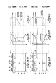
- FIG. 1A represents a sectional, schematic view of a conventional field controlled thyristor structure:
- FIG. 1B is a graphical illustration of the doping profile for the device of FIG. 1A, with dopant concentration at section 1--1' in FIG. 1A plotted along the abscissa and depth beneath the uppermost surface of the device plotted along the ordinate:
- FIG. 1C is a graphical representation of the electric field distribution in the device of FIG. 1A, with electric field strength at section 1--1' in FIG. 1A plotted along the abscissa and depth beneath the uppermost surface of the device plotted along the ordinate;
- FIG. 1D illustrates the location of the depletion layer in the device of FIG. 1A
- FIG. 2A represents a sectional, schematic view of the asymmetrical field controlled thyristor structure of the present invention
- FIG. 2B is a graphical illustration of the doping profile for the device of FIG. 2A, with dopant concentration at section 2--2' in FIG. 2A plotted along the abscissa and depth beneath the uppermost surface of the device plotted along the ordinate;
- FIG. 2C is a graphical representation of the electric field distribution in the device of FIG. 2A, with electric field strength at section 2--2' in FIG. 2A plotted along the abscissa and depth beneath the uppermost surface of the device plotted along the ordinate;
- FIG. 2D illustrates the location of the depletion layer in the device of FIG. 2A.
- FIG. 3A depicts an N type silicon wafer and oxide layer initially produced during the fabrication of the asymmetrical field controlled thyristor of the present invention
- FIG. 3B illustrates the structure of FIG. 3A after oxide removal and a phosphorus diffusion on the lowermost or back surface of the wafer
- FIG. 3C depicts the structure of FIG. 3B after fabrication of anode and gate regions
- FIG. 3D illustrates the structure of FIG. 3C subsequent creation of the source or cathode region
- FIG. 3E depicts the structure of FIG. 3D after fabrication of gate and cathode contacts.
- FIG. 3F represents the completed asymmetrical field controlled thyristor structure of the present invention with an anode contact established on the underside of the wafer.
- a conventional field controlled thhristor is illustrated as comprised of semiconductor material with an N type base region 10, a P+ anode region 12, P+ grid regions 13, and an N+ cathode region 14.
- N base region 10 forms gate interfaces 8 and a cathode interface 9 with gate regions 13 and cathode region 14, respectively, and forms an anode interface 18 with anode region 12.
- Cathode, grid and anode contacts 15, 16 and 17, respectively, are provided, typically in the form of aluminum metallization, with the remainder of the uppermost surface of the device passivated by silicon oxide layer 19.
- the asymmetrical field controlled thyristor of the instant invention is illustrated as comprised of semiconductor material with a dual-layer N type base including a lightly doped N- portion 30 and a more heavily doped N portion 31.
- the remainder of the structure is similar to that of FIG. 1A in that it includes a P+ anode region 32, P+ grid regions 33, and an N+cathode region 34.
- N- base layer 30 forms gate interfaces 41 and a cathode interface 42 with gate regions 33 and cathode region 34, respectively, and N+ base layer 31 forms an anode interface 43 with anode region 32.
- Cathode, grid and anode contacts 35, 36 and 37, respectively, are provided, typically in the form of aluminum metallization, and the remainder of the uppermost surface of the device is passivated by silicon oxide layer 39.
- FIGS. 2A and 1A Associated with the devices of FIGS. 2A and 1A are the doping profiles of the respective devices, shown in FIGS. 2B and 1B, respectively, and the electric field distribution in the respective devices during both forward blocking and reverse blocking, as shown in FIGS. 2C and 1C, respectively.
- the field controlled thyristor of the present invention shown in FIG. 2A, should be contrasted with the conventional device structure shown in FIG. 1A.
- the structure illustrated of the device of the present invention is similar to that of a conventional field controlled thyristor except that the N base of the device of the present invention comprises a two layer N base made up of very lightly doped region 30 near the gate and cathode regions and more heavily doped region 31 near the anode region.
- This modification of the doping profile exerts a strong influence upon electric field distribution in both the forward and reverse blocking stages of device operation which, in turn, results in significant improvement in forward blocking capability as described, infra.
- the change in doping profile also results in a significant improvement in forward voltage drop.
- the transistor punch-through breakdown is prevented by incorporating into the N base a more heavily doped region 31 near the anode. This allows use of a very low doping level for the remainder 30 of the N base without encountering the open base transistor breakdown effect.
- the gate depletion layer extending to the dashed line in N base layer 31 as shown in FIG. 2D, contains a low ionized impurity density which results in maintaining a high electric field throughout the depth of lightly doped N-base portion 30, as shown in FIG. 2C.
- the electric field then decreases very sharply in the more heavily doped N base region 31, thus preventing punch-through breakdown.
- the uniform doping of N base 10 in the conventional device structure shown in FIG. 1A produces a steadily decreasing electric field in N base 10 with its peak at gate junction 8, as shown in FIG. 1C.
- FIGS. 1C and 2C Because the voltage supported between the gate and anode terminals is given by the area under the electric field profile, it is evident from FIGS. 1C and 2C that, during forward blocking conditions, the structure of FIG. 2A exhibits a substantially higher breakdown voltage for the same total wafer thickness and junction diffusion depths than the structure of FIG. 1A. There is, however, no substantial difference in forward voltage drop during current conduction since the two devices are alike in wafer thickness and in junction depths of anode and cathode regions. Thus the N base doping profile for the device of FIG. 2A results in a higher forward blocking capability than that of the device in FIG. 1A, while maintaining the same forward voltage drop during current conduction.
- N base resistivity is substantially 35 ohm-cm.
- this N base material has a depletion width of substantially 90 micrometers. Since a diffusion length of at least 40 micrometers is required to maintain a low forward voltage drop, the total N base width of the conventional device would be about 130 micrometers. In the new device structure, however, thickness of more heavily doped N base portion 31 is about 30 micrometers to prevent gate depletion layer punch-through to anode region 32.
- the lightly doped N-base portion 30 of the new device structure would have a thickness of about 100 micrometers.
- the low doping level of this region results in a uniform electric field, as shown in FIG. 2C, which has a value E p of about 2 ⁇ 10 5 V/cm at breakdown as pointed out in S.M. Sze and G. Gibbons, "Avalanche Breakdown Voltages of Abrupt and Linearly Graded p-n Junctions in Ge, Si, GaAs, and GaP", Applied Physics Letters, Vol. 8, pp 111-113 (1976).
- forward blocking capability of the device of FIG. 1A extends to about 2,000 volts.
- a twofold increase in blocking voltage can be expected while maintaining the same forward voltage drop.
- N-base portion 30 Use of lightly doped N-base portion 30 in the gate area of the device of FIG. 2A results in a very large increase in blocking gain over devices of the type shown in FIG. 1A. Since the doping level of the entire N base is lower in region 30, the depletion layers from gate regions 33 extend into the channel area at lower gate voltages than from gate regions 13 in the device shown in FIG. 1A. As a result, the anode-cathode current is pinched off at a lower gate voltage than in the device shown in FIG. 1A, thus providing increased blocking gain. Moreover, if channel width is small and N- base portion 30 is very lightly doped, the diffusion potential of gate junctions 41 can be sufficient to cause gate depletion layer punch-through under the channel.
- anode-cathode current flow terminates with zero bias on the gate.
- the potential barrier in the channel at zero gate bias is small and can therefore prevent anode-cathode current flow only at anode voltages below 100 volts.
- high blocking gains can be obtained by use of the planar diffusion process, eliminating need for use of the more complex epitaxial-refill technology that has heretofore been required to achieve high blocking gains. Device processing yields may consequently be expected to improve.
- FIG. 2A Another significant advantage of the structure shown in FIG. 2A is improved gate turn-off capability.
- gate turn-off is achieved at gate voltages which create a depletion layer that pinches off the anode-cathode current, but with the depletion layer extending only a short distance from the gate junction as shown in FIG. 1D.
- the gate depletion layer sweeps out only a small fraction of the charge which is injected into N base 10 during forward conduction. The remaining charge in N base 10 must then decay by recombination. This causes the anode-cathode current to gradually tail off, decreasing switching speed of the device.
- Fabrication of the asymmetrical field controlled thyristor of the present invention begins with high resistivity, N type silicon wafers, such as wafer 30, shown in FIG. 3A.
- a typical resistivity is 2,000 ohm-cm, although resistivity above 50 ohm-cm is suitable, depending upon the breakdown voltage desired for the device.
- the higher resistivities should be selected for devices requiring higher breakdown voltages and high blocking gains.
- Wafer 30 is first oxidized, preferably in a steam-oxygen mixture at 1150° C., to obtain a silicon oxide layer of 10,000 angstroms on the surface. This oxide layer is then removed on the lowermost or back surface 40 of the wafer, which is to serve as the anode region of the device being fabricated, leaving oxide layer 39 on the upper surface.
- a phosphorous diffusion is performed on back surface 40 of the wafer to obtain a diffused layer 31 with a surface concentration of about 2 ⁇ 10 17 dopant atoms per cc and a depth of 30-50 micrometers.
- Typical phosphorous deposition may be performed at 800° C. for 30 minutes using phosphorous oxychloride, followed by a drive-in cycle at 1250° C. for 50 hours, resulting in the structure shown in FIG. 3B.
- Oxide layer 39 on the uppermost or front surface of the wafer is next patterned using conventional photolithography to open the gate diffusion area, and oxide on back surface 40 of the wafer is also removed at this time.
- a boron diffusion is then performed on both sides of the wafer, so as to diffuse boron therein through both major surfaces of the wafer. Typical diffusion may be performed at 975° C. for one hour using boron nitride source wafers, followed by a drive-in cycle at 1250° C. for two hours. This diffusion simultaneously creates anode region 32 and gate regions 33, with a surface concentration of about 1 ⁇ 10 19 cm -3 and a junction depth of about 5 micrometers, as shown in FIG. 3C. However, separate boron diffusions may alternatively be performed to fabricate these regions if desired.
- Oxide layer 39 on the front surface of the wafer is next patterned by conventional photolithography to open the cathode diffusion area.
- the oxide layer 44 formed on the back surface of the wafer is not removed during this step.
- a phosphorous diffusion is then performed to create the source or cathode region 34.
- Diffusion is typically performed with a deposition at 900° C. for 30 minutes followed by a drive-in cycle at 1000° C. for 30 minutes to obtain a junction depth of 1.5 micrometers and a surface concentration of 1 ⁇ 10 19 cm -3 resulting in the structure shown in FIG. 3D.
- Oxide layer 39 is again photolithographically patterned to open contact windows for the cathode and gate, while the oxide layer on back surface 40 is removed to open a contact area for the anode.
- Aluminum is then evaporated on the front surface to a thickness of 1-2 micrometers, and patterned photolithographically to obtain contacts 35 and 36 to the gate and cathode areas, respectively, as shown in FIG. 3E.
- An aluminum layer 37 is next evaporated on the anode side of the wafer, and sintered at 400° C. for 30 minutes to lower contact resistance, resulting in the structure illustrated in FIG. 3F.
- a typical device formed according to the aforementioned processing steps may be fabricated with a plurality of cathode fingers, each cathode finger having a width of 10 micrometers and a length of 750 micrometers.
- the cathode fingers are interdigitated with, and surrounded by, the gate region. Breakdown voltage of these devices has been found to increase with wafer thickness (or depth), and ranges from 500 volts for wafers of 5 mil thickness to 1000 volts for wafers of 10 mil thickness.
- the fabricated device can block an anode voltage of over 950 volts with an applied gate bias of but 14 volts, so that DC blocking gain exceeds 65.
- Blocking gain of the asymmetrical field controlled thyristors fabricated in accordance with the present invention has been found to be a function of N base thickness, even with gate junction depth held unchanged; that is, maximum anode blocking voltage increases with N base width. This is to be expected since the high electric field is maintained over a wider N base as wafer thickness increases.
- blocking gain has also been found to be dependent upon N base width, and increases by more than a factor of 3 in going from a base width of 65 micrometers to a base width of 190 micrometers. This dependence of the blocking gain on the N base width arises from the very low N base doping level, which results in the gate depletion layer extending across the entire N base of these devices for all wafer thicknesses, under forward blocking conditions. The pinch-off region in the channel, therefore, extends all the way from cathode 34 to N type diffused buffer layer 31.
- the device of FIG. 2A is designed to allow the gate depletion layer to punch through in the channel region without any applied gate bias. This gives the device ability to block anode current even without an applied reverse gate bias.
- the potential barrier created in the channel by the inherent potential of gate junction 41 is sufficient to block current flow only at low anode voltages; that is, as anode voltage is increased, the device switches from the blocking state to the conductive state.
- the device of FIG. 2A When the device of FIG. 2A is operating in the conductive state, its characteristics resemble those of a rectifier diode. At low anode currents, the device current increases exponentially with anode voltage and the device exhibits a low forward voltage drop due to conductivity modulation of the dual-layer N base by the injected holes and electrons from the anode and cathode regions, respectively. This conductivity modulation decreases as N base width is increased, and results in an increase in forward voltage drop with increasing base width. While the effect of increasing the base width on forward voltage drop is small at low current densities, it becomes quite severe at higher current densities. At a device current of 10 amperes, cathode current density exceeds 1000 A/cm 2 .
- the foregoing describes a field controlled thyristor with gate turn-off capability and high blocking gain.
- the device exhibits a low forward voltage drop and a high speed switching capability.
- the power field controlled thyristor of the invention readily lends itself to fabrication by conventional planar semiconductor diffusion technology.
Abstract
Description
Claims (20)
Priority Applications (1)
| Application Number | Priority Date | Filing Date | Title |
|---|---|---|---|
| US06/756,478 US4937644A (en) | 1979-11-16 | 1985-07-17 | Asymmetrical field controlled thyristor |
Applications Claiming Priority (2)
| Application Number | Priority Date | Filing Date | Title |
|---|---|---|---|
| US9494379A | 1979-11-16 | 1979-11-16 | |
| US06/756,478 US4937644A (en) | 1979-11-16 | 1985-07-17 | Asymmetrical field controlled thyristor |
Related Parent Applications (1)
| Application Number | Title | Priority Date | Filing Date |
|---|---|---|---|
| US06597895 Continuation | 1984-04-09 |
Publications (1)
| Publication Number | Publication Date |
|---|---|
| US4937644A true US4937644A (en) | 1990-06-26 |
Family
ID=26789363
Family Applications (1)
| Application Number | Title | Priority Date | Filing Date |
|---|---|---|---|
| US06/756,478 Expired - Lifetime US4937644A (en) | 1979-11-16 | 1985-07-17 | Asymmetrical field controlled thyristor |
Country Status (1)
| Country | Link |
|---|---|
| US (1) | US4937644A (en) |
Cited By (6)
| Publication number | Priority date | Publication date | Assignee | Title |
|---|---|---|---|---|
| US5317171A (en) * | 1992-04-29 | 1994-05-31 | North Carolina State University | MOS gated thyristor with remote turn-off electrode |
| US5319222A (en) * | 1992-04-29 | 1994-06-07 | North Carolina State University | MOS gated thyristor having on-state current saturation capability |
| US6011279A (en) * | 1997-04-30 | 2000-01-04 | Cree Research, Inc. | Silicon carbide field controlled bipolar switch |
| US20090168660A1 (en) * | 2007-12-28 | 2009-07-02 | United States Cellular Corporation | Zero rating in wireless prepaid communications network |
| US20130281959A1 (en) * | 2005-06-02 | 2013-10-24 | The Procter & Gamble Company | Absorbent article having traverse reinforcing element |
| CN104392911A (en) * | 2014-10-31 | 2015-03-04 | 宁波芯科电力半导体有限公司 | Boron diffusion method of high-voltage thyristor chips |
Citations (6)
| Publication number | Priority date | Publication date | Assignee | Title |
|---|---|---|---|---|
| US3409812A (en) * | 1965-11-12 | 1968-11-05 | Hughes Aircraft Co | Space-charge-limited current triode device |
| US3465216A (en) * | 1966-07-22 | 1969-09-02 | Stanislas Teszner | Bistable semiconductor device for heavy currents |
| US3482151A (en) * | 1967-04-11 | 1969-12-02 | Stanislas Teszner | Bistable semiconductor integrated device |
| US3497777A (en) * | 1967-06-13 | 1970-02-24 | Stanislas Teszner | Multichannel field-effect semi-conductor device |
| US3814995A (en) * | 1972-03-10 | 1974-06-04 | S Teszner | Field-effect gridistor-type transistor structure |
| US4223328A (en) * | 1977-06-08 | 1980-09-16 | Hitachi, Ltd. | Field controlled thyristor with dual resistivity field layer |
-
1985
- 1985-07-17 US US06/756,478 patent/US4937644A/en not_active Expired - Lifetime
Patent Citations (6)
| Publication number | Priority date | Publication date | Assignee | Title |
|---|---|---|---|---|
| US3409812A (en) * | 1965-11-12 | 1968-11-05 | Hughes Aircraft Co | Space-charge-limited current triode device |
| US3465216A (en) * | 1966-07-22 | 1969-09-02 | Stanislas Teszner | Bistable semiconductor device for heavy currents |
| US3482151A (en) * | 1967-04-11 | 1969-12-02 | Stanislas Teszner | Bistable semiconductor integrated device |
| US3497777A (en) * | 1967-06-13 | 1970-02-24 | Stanislas Teszner | Multichannel field-effect semi-conductor device |
| US3814995A (en) * | 1972-03-10 | 1974-06-04 | S Teszner | Field-effect gridistor-type transistor structure |
| US4223328A (en) * | 1977-06-08 | 1980-09-16 | Hitachi, Ltd. | Field controlled thyristor with dual resistivity field layer |
Cited By (9)
| Publication number | Priority date | Publication date | Assignee | Title |
|---|---|---|---|---|
| US5317171A (en) * | 1992-04-29 | 1994-05-31 | North Carolina State University | MOS gated thyristor with remote turn-off electrode |
| US5319222A (en) * | 1992-04-29 | 1994-06-07 | North Carolina State University | MOS gated thyristor having on-state current saturation capability |
| US6011279A (en) * | 1997-04-30 | 2000-01-04 | Cree Research, Inc. | Silicon carbide field controlled bipolar switch |
| US20130281959A1 (en) * | 2005-06-02 | 2013-10-24 | The Procter & Gamble Company | Absorbent article having traverse reinforcing element |
| US8878000B2 (en) * | 2005-06-02 | 2014-11-04 | The Procter & Gamble Company | Absorbent article having traverse reinforcing element |
| US20090168660A1 (en) * | 2007-12-28 | 2009-07-02 | United States Cellular Corporation | Zero rating in wireless prepaid communications network |
| US7701870B2 (en) | 2007-12-28 | 2010-04-20 | United States Cellular Corporation | Zero rating in wireless prepaid communications network |
| CN104392911A (en) * | 2014-10-31 | 2015-03-04 | 宁波芯科电力半导体有限公司 | Boron diffusion method of high-voltage thyristor chips |
| CN104392911B (en) * | 2014-10-31 | 2017-04-12 | 宁波芯科电力半导体有限公司 | Boron diffusion method of high-voltage thyristor chips |
Similar Documents
| Publication | Publication Date | Title |
|---|---|---|
| US4982260A (en) | Power rectifier with trenches | |
| US5241195A (en) | Merged P-I-N/Schottky power rectifier having extended P-I-N junction | |
| US4292642A (en) | Semiconductor device | |
| US4223328A (en) | Field controlled thyristor with dual resistivity field layer | |
| US4935798A (en) | Static induction type thyristor | |
| US4060821A (en) | Field controlled thyristor with buried grid | |
| US4037245A (en) | Electric field controlled diode with a current controlling surface grid | |
| US6011279A (en) | Silicon carbide field controlled bipolar switch | |
| KR20000010929A (en) | Schottky barrier rectifiers and methods of forming same | |
| US6674152B2 (en) | Bipolar diode | |
| US5387805A (en) | Field controlled thyristor | |
| US4476481A (en) | Low-loss P-i-n diode | |
| US20170256614A1 (en) | Vertical insulated gate turn-off thyristor with intermediate p+ layer in p-base | |
| US5270230A (en) | Method for making a conductivity modulation MOSFET | |
| US4089020A (en) | High power semiconductor diode | |
| US4171995A (en) | Epitaxial deposition process for producing an electrostatic induction type thyristor | |
| EP0029932B1 (en) | Asymmetrical field controlled thyristor | |
| EP0454201B1 (en) | A semiconductor device comprising a thyristor | |
| US4937644A (en) | Asymmetrical field controlled thyristor | |
| Baliga | The asymmetrical field-controlled thyristor | |
| US5504351A (en) | Insulated gate semiconductor device | |
| US5057440A (en) | Manufacturing gate turn-off thyristor having the cathode produced in two diffusion steps | |
| US4569118A (en) | Planar gate turn-off field controlled thyristors and planar junction gate field effect transistors, and method of making same | |
| GB2612636A (en) | Semiconductor device | |
| US4829349A (en) | Transistor having voltage-controlled thermionic emission |
Legal Events
| Date | Code | Title | Description |
|---|---|---|---|
| STCF | Information on status: patent grant |
Free format text: PATENTED CASE |
|
| FEPP | Fee payment procedure |
Free format text: PAYOR NUMBER ASSIGNED (ORIGINAL EVENT CODE: ASPN); ENTITY STATUS OF PATENT OWNER: LARGE ENTITY |
|
| FPAY | Fee payment |
Year of fee payment: 4 |
|
| FPAY | Fee payment |
Year of fee payment: 8 |
|
| AS | Assignment |
Owner name: INTERSIL CORPORATION, FLORIDA Free format text: ASSIGNMENT OF ASSIGNORS INTEREST;ASSIGNOR:HARRIS CORPORATION;REEL/FRAME:010255/0405 Effective date: 19990813 |
|
| AS | Assignment |
Owner name: CREDIT SUISSE FIRST BOSTON, AS COLLATERAL AGENT, N Free format text: SECURITY INTEREST;ASSIGNOR:INTERSIL CORPORATION;REEL/FRAME:010351/0410 Effective date: 19990813 |
|
| AS | Assignment |
Owner name: INTERSIL HOLDING CORPORATION, CALIFORNIA Free format text: INTELLECTUAL PROPERTY PARTIAL RELEASE;ASSIGNOR:CREIDT SUISSE FIRST BOSTON;REEL/FRAME:011667/0166 Effective date: 20010303 |
|
| AS | Assignment |
Owner name: FAIRCHILD SEMICONDUCTOR CORPORATION, MAINE Free format text: REASSIGNMENT OF PATENT APPLICATIONS;ASSIGNOR:INTERSIL CORPORATION;REEL/FRAME:012002/0206 Effective date: 20010406 |
|
| FPAY | Fee payment |
Year of fee payment: 12 |
|
| REMI | Maintenance fee reminder mailed |