US4933952A - Asynchronous digital correlator and demodulators including a correlator of this type - Google Patents
Asynchronous digital correlator and demodulators including a correlator of this type Download PDFInfo
- Publication number
- US4933952A US4933952A US07/332,968 US33296889A US4933952A US 4933952 A US4933952 A US 4933952A US 33296889 A US33296889 A US 33296889A US 4933952 A US4933952 A US 4933952A
- Authority
- US
- United States
- Prior art keywords
- values
- bit
- carrier
- correlation
- cell
- Prior art date
- Legal status (The legal status is an assumption and is not a legal conclusion. Google has not performed a legal analysis and makes no representation as to the accuracy of the status listed.)
- Expired - Fee Related
Links
Images


Classifications
-
- H—ELECTRICITY
- H04—ELECTRIC COMMUNICATION TECHNIQUE
- H04B—TRANSMISSION
- H04B1/00—Details of transmission systems, not covered by a single one of groups H04B3/00 - H04B13/00; Details of transmission systems not characterised by the medium used for transmission
- H04B1/69—Spread spectrum techniques
- H04B1/707—Spread spectrum techniques using direct sequence modulation
- H04B1/709—Correlator structure
-
- G—PHYSICS
- G06—COMPUTING; CALCULATING OR COUNTING
- G06F—ELECTRIC DIGITAL DATA PROCESSING
- G06F17/00—Digital computing or data processing equipment or methods, specially adapted for specific functions
- G06F17/10—Complex mathematical operations
- G06F17/15—Correlation function computation including computation of convolution operations
-
- H—ELECTRICITY
- H04—ELECTRIC COMMUNICATION TECHNIQUE
- H04B—TRANSMISSION
- H04B1/00—Details of transmission systems, not covered by a single one of groups H04B3/00 - H04B13/00; Details of transmission systems not characterised by the medium used for transmission
- H04B1/69—Spread spectrum techniques
- H04B1/707—Spread spectrum techniques using direct sequence modulation
- H04B1/70718—Spread spectrum techniques using direct sequence modulation with asynchronous demodulation, i.e. not requiring code synchronisation
-
- H—ELECTRICITY
- H04—ELECTRIC COMMUNICATION TECHNIQUE
- H04L—TRANSMISSION OF DIGITAL INFORMATION, e.g. TELEGRAPHIC COMMUNICATION
- H04L23/00—Apparatus or local circuits for systems other than those covered by groups H04L15/00 - H04L21/00
- H04L23/02—Apparatus or local circuits for systems other than those covered by groups H04L15/00 - H04L21/00 adapted for orthogonal signalling
-
- H—ELECTRICITY
- H04—ELECTRIC COMMUNICATION TECHNIQUE
- H04L—TRANSMISSION OF DIGITAL INFORMATION, e.g. TELEGRAPHIC COMMUNICATION
- H04L27/00—Modulated-carrier systems
- H04L27/18—Phase-modulated carrier systems, i.e. using phase-shift keying
- H04L27/22—Demodulator circuits; Receiver circuits
- H04L27/227—Demodulator circuits; Receiver circuits using coherent demodulation
- H04L27/2275—Demodulator circuits; Receiver circuits using coherent demodulation wherein the carrier recovery circuit uses the received modulated signals
- H04L27/2278—Demodulator circuits; Receiver circuits using coherent demodulation wherein the carrier recovery circuit uses the received modulated signals using correlation techniques, e.g. for spread spectrum signals
-
- H—ELECTRICITY
- H04—ELECTRIC COMMUNICATION TECHNIQUE
- H04J—MULTIPLEX COMMUNICATION
- H04J13/00—Code division multiplex systems
- H04J13/0007—Code type
- H04J13/0022—PN, e.g. Kronecker
- H04J13/0025—M-sequences
Definitions
- the invention concerns an asynchronous digital correlator and demodulators having a correlator of this type.
- This correlator enables the processing of a complex signal formed by a first carrier and a second carrier, I and Q, modulated by a pseudo-random function to spread the spectrum and modulate it by an M-ary orthogonal code.
- a complex signal of this type results, for example, from a PSK, MSK or APSK type modulation with spectrum spreading, and modulation by Walsh codes.
- the demodulation of a signal of this type makes it necessary to compress its spectrum by means of a pseudo-random function identical to the one thathas been used to spread this spectrum, and then consists in recognizing a transmitted item of data in identifying the modulating among M possible codes. These two operations can be done by means of a correlator.
- correlators that can be used to correlate a complex signal with a reference signal on a great length, such as one of 256 chips, while having, at the same time, a structure that is simple enough to enable the making of a demodulator which can be integrated in a single integrated circuit.
- Prior art types of correlators are designed for frame recognition rather than for demodulation.
- a first type of prior art correlator device commercially available in the form of an integrated circuit, works only on 64 chips.
- a second known type of correlator commercially available in integrated circuit form, works on 256 chips and has no intermediate outputs giving partial correlation values relating to a smaller number of chips.
- Known correlators have a large number of 64-chip or 256-chip correlators: they have a chain of four 64-chip correlators, or one 256-chip correlator for the carrier I; and a chain of four 64-chip correlators or one 256-chip correlator for the carrier Q, for each of the M-ary codes. Since number M may be equal to 16, the number of integrated circuits may reach 128.
- An aim of the invention is to propose an asynchronous digital correlator that enables the making, notably, of simpler demodulators which may possibly be integrated in a small number of integrated circuits or even in a single integrated circuit.
- An object of the invention is a correlator with a systolic structure wherein the computations for the carrier I and the carrier Q are temporally multiplexed, said structure being divided in such a way that it gives values of the modulus of a partial correlation function computed on far smaller lengths than the total correlation length, to enable recognition of the codes by means of a relatively simple arithmetic code computing linear combinations of these moduluses.
- an asynchronous, digital correlator to correlate a binary reference signal (REF) with a complex signal formed by a first carrier and second carrier (I, Q), modulated by a pseudo-random function and by an M-ary orthogonal encoding, said two carriers being sampled and digitized, said correlator comprising:
- a multiplexer to transmit, alternately, a value (I) of the first carrier, and a value (Q) of the second carrier, with a period equal to half their sampling period;
- a first digital filter adapted to the pseudo-random function (PN), comprising a chain of registers to store L consecutive bits of the reference signal (REF) and a chain of M correlation macro-cells receiving the sequence of multiplexed values of the first carrier and the second carrier (I and Q), each macro-cell computing the value (CPI0,..., CPI15) of a first function, called a partial correlation function, between N bits of the reference signal and N values of the first carrier (I), and then computing the value (CPQ0,..., CPQ15) of a second function, called a partial correlation function, betweenn N bits of the reference signal and N values of the second carrier (Q), N being equal to L/M;
- PN pseudo-random function
- a second digital filter adapted to at least one of the M-ary encoding codes and having computation means to determine the value of at least one linear combination of the values of the first functions of partial correlation (CPI0,... CPI15); and then to determine the value of a linear combination of the values of the second functions of partial correlation (CPQ0,..., CPQ15), the coefficients of the linear combination being unchanged and being equal to ⁇ 1; and having means to demultiplex the values of the two linear combinations (FIi, FQi), and to determine the modulus (Fi) of a vector having, as its components, the values of these two linear combinations (FIi, FQi).
- FIG. 1 is a block diagram of an exemplary embodiment of a prior art demodulator
- FIG. 2 is a block diagram of an exemplary embodiment of a first type of demodulator including a correlator according to the invention
- FIG. 3 shows a more detailed block diagram of a correlation macro-cell constituting this exemplary embodiment
- FIGS. 4 and 5 are partial diagrams of this macro-cell
- FIG. 6 is a block diagram of a computing device belonging to this exemplary embodiment
- FIG. 7 shows a block diagram of an exemplary embodiment of a second type of demodulator including a correlator according to the invention.
- FIG. 8 shows a block diagram of a computing device belonging to this embodiment.
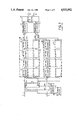
- the prior art demodulator shown in FIG. 1, has:
- two input terminals 1 and 2 respectively receiving the digital values of two carriers, I and Q, which are modulated by a pseudo-random function and by an M-ary orthogonal code, and which are sampled and digitized;
- a Walsh codes generator 13 having 16 outputs, respectively giving 16 binary signals corresponding to 16 Walsh codes, and referenced W0, ...W15;
- a generator 14 giving a pseudo-random binary signal PN, identical to the one that has been used to spread the spectrum of the two carrier waves I and Q;
- each chain such as the chain 100 having four correlators 5 to 8, each operating on 64 chips and being formed by an integrating circuit;
- each of the chains 100 to 115 and 200 to 215 by means of a single correlator integrated circuit working on 256 chips.
- the chains of correlators 100 to 115 respectively give digital values F10 to F115, which are the values of the functions of correlation of the carrier 1, respectively with the sixteen reference signals, on 256 chips.
- Each of the computing devices of the set 9 computes the modulus of a vector having, as its components, a value of the function of correlation of the carrier 1 with a reference signal corresponding to a code and a value of the function of correlation of the carrier Q with the same reference signal. For example, a computing device of the set 9 computes the square root of F10 2 +FQ0 2 .
- the set 9 gives the sixteen values, F0 to F15 of the moduluses of the functions of correlation of the complex signal formed by the carrier I and the carrier Q, correlated with the sixteen reference signals.
- the sixteen vales F0 to F15 are compared with one another by the device 10.
- This device 10 gives an output terminal 19 the index j of the correlation function with the greatest modulus. This index j designates the code that modulates the carriers I and Q.
- the device 10 also gives the value Fj of the modulus to a output terminal 20.
- This prior art demodulator is complex and bulky because there are 32 correlation chains in parallel.
- FIG. 2 is a block diagram of an exemplary embodiment of a demodulator of a first type, having a correlator according to the invention.
- This demodulator has five sub-units:
- a multiplexer 33 to transmit, alternately, a value of the carrier I and a value of the carrier Q, at a rate which is twice their sampling frequency;
- a first digital filter 31 adapted to the pseudo-random function, which spreads the spectrum of the carriers I and Q;
- a second digital filter 35 matched to the sixteen Walsh codes which can modulate the carriers I and Q to transmit a piece of data; this latter filter computes sixteen values of moduluses of correlation functions, F0 to F15, corresponding to sixteen Walsh codes;
- a device 34 selecting the maximum among these sixteen values, and giving the maximum value Fj to an output terminal 28 and giving the index j, which identifies the modulating code, at an output terminal 25.
- the first digital filter 31 has:
- a generator 24 giving a pseudo-random signal PN, identical to the one used to spread the spectrum of the complex signal to be demodulated;
- a multiplexer 23 having two data inputs, one output and one control input.
- the pseudo-random signal PN is a reference signal, REF, for demodulation.
- the bits of the signal REF are stored and shifted, one by one, in the chain of registers 40 under the control of a clock signal CKR, at the rate at which they are created by the generator 24.
- the signal CKR is given to an input terminal 25 by a standard generator of clock signals, not shown in the figure.
- the chain of registers 40 stores 256 bits of the reference signal.
- the content of these registers is transferred as a block into the chain of registers 40, under the control of a clock signal, LOAD, in synchronism with the clock signal CKS.
- the period of the signal LOAD is, for example, 10 mS, while that of CKR is, for example, 30 nS.
- the clock signal LOAD is given to an input terminal 26 by a standard generator of clock signals, not shown in the figure.
- the multiplexer 23 is a multiplexer with two inputs and one output. Its inputs are respectively connected to input terminals 21 and 22, receiving the carriers I and Q to be demodulated, in the form of digital values encoded on four bits, the negative values being encoded in the two's complement system.
- the output of the multiplexer 23 gives a value formed by four bits: X0, ..., X3 to an input of the chain 43, with sixteen correlation macro-cells.
- the multiplexer 23 and the correlation macro-cells are controlled by a clock signal CKS at a rate which is twice the sampling rate of the carriers I and Q.
- the clock signal CKS is given to an input terminal 27 by a standard generator of clock signals, not shown in FIG. 2.
- the first correlation cell in the chain 42 is a cell 43 which receives the four bits X0, ..., X3, alternately representing a value of the carrier I and a value of the carrier Q, and which receives 32 bits R0, ..., R15, R0 ..., R15, representing sixteen bits of the reference signal stored in a register of the chain 41.
- the macro-cell 43 retransmits the four bits X0, X3 to a following macro-cell, with a delay respectively equal to 16, 17, 18, 19 periods of the clock signal CKS, and respectively gives a value CPI0 of the partial correlation function corresponding to the signal I, then a value CPQ0 of the partial correlation function corresponding to the signal Q.
- Each macro-cell is identical to the macro-cell 43 and has: a sixteen bit input receiving sixteen successive bits of the reference signal and sixteen complementary bits; a four bit input receiving a value of the sequence of multiplexed values of the carriers I and Q; an output retransmitting the four bits of this value to the following macro-cell, with a delay respectively equal to 16, 17, 18, 19 periods of the clock signal CKS; and an eight bit output successively giving the value of a first partial correlation function, corresponding to the carrier I, then the value of a second partial correlation function corresponding to the carrier Q, said output being connected to an input of the linear combinations computing device 32.
- the chain of correlators 42 has 16 eight-bit outputs respectively giving sixteen values of partial correlation functions: CPI0, CPI15, corresponding to the carrier I; and then respectively giving sixteen values of partial correlation functions: CPQ0, CPQ15, correspondig to the carrier Q.
- the filter 35 has: a device 32 for the computation of linear combinations and a demultiplexing and modulus computing device 33.
- the reference signal REF is formed solely by the pseudo-random signal PN, contrary to the reference signals used in the prior art device shown in FIG. 1.
- the device 32 is a "pipeline" structure device controlled by the clock signal CKS. It has two eight-bit outputs, respectively giving values FI0, ..., FI15 which are values of the function of correlation of the signal I with the reference signal and with the sixteen Walsh codes respectively; then respectively giving values FQ0, ..., FQ15 which are values of the function of correlation of the signal Q with the reference signal and with sixteen Walsh codes respectively.
- the device 33 has sixteen outputs giving, respectively, the values F0, F15, to sixteen inputs of the device 34.
- This index j designates the Walsh code which is detected by the demodulator. In other words, it designates the piece of data which is transmitted by the signals I and Q.
- the devices 32, 33 and 34 are also controlled by the clock signal CKS.
- FIG. 3 shows a block diagram of the macro-cell 43.
- the other macro-cells of the chain 42 are identical to the macro-cell 43.
- Each macro-cell has a systolic structure formed by a matrix of 128 identical cells working on a single bit. This matrix has eight rows of sixteen cells.
- the first cell 49, of the first row of cells receives a bit X0 of a first value from the carrier I or Q. This bit X0 is propagated from one cell to another of the first row, each delay being equal to a clock signal CKS period.
- the first cell of the second row of the matrix receives the bit Xl with a delay equal to the clock signal CKS period, with reference to the bit X0. This delay is got by a D-type flip-flop 57.
- the cells of the second row retransmit the bit Xl, each with a delay equal to a clock signal CKS period.
- the first cell of the third row receives the bit X2 with a delay equal to two clock signal CKS periods: this delay is obtained by a set 58 formed by two D-type flip-flops.
- the cells of the third row retransmit the bit X2, each with a delay equal to one clock signal CKS period.
- the first cell of the third row receives the bit X3 with a delay equal to three clock signal CKS periods. This delay is got by a set 59 of three D-type flip-flops.
- the cells of the third line retransmit the bit X3,. each with a delay equal to a clock signal CKS period.
- the first cell of the fourth row receives the bit X3 with a delay equal to three clock signal CKS periods: this delay is got by a set 59 of three D-type flip-flops. Each cell of the fourth row retransmits the bit X3 with a delay equal to a clock signal CKS period.
- the first cell of the fifth line receives the bit X3 with a delay equal to four clock signal CKS periods. This delay is got by a set 60 of four D-type flip-flops. Each cell of the fifth line retransmits the X3 with a delay equal to a clock signal CKS period.
- the first cell of the eighth row receives the bit X3 with a delay equal to seven periods of the clock signal CKS. This delay is obtained by a set 63 of seven D-type flip-flops. Each cell of the eighth row retransmits the bit X3 with a delay equal to a clock signal CKS period.
- the first cell of the sixth line receives the bit X3 with a delay equal to five clock signal CKS periods.
- the delay is got by a set 61 of five D-type flip-flops.
- Each cell of the sixth row retransmits the bit X3 with a delay equal to a clock signal CKS period.
- the first cell of the seventh row receives the bit X3 with a delay equal to six periods of the clock signal CKS.
- This delay is got by a set 62 of six D-type flip-flops.
- Each cell of the seventh row retransmits the bit X3 with a delay equal to one clock signal CKS period.
- the last cell of each line therefore gives one of the bits X0, Xl, X2, X3, with a delay which depends on the order of the row, to an input of the following macro-cell in the chain 42.
- Each cell has an input receiving one partial correlation result bit, given by an output, called a partial correlation result output, belonging to the next cell.
- a partial correlation result output belonging to the next cell.
- the capacity of a macro-cell is never exceeded. Consequently, there is no provision for transmitting result bits from one macro-cell to another.
- the inputs of the partial correlation result bits of the last cells respectively receive bits C0,..., C7 having null value.
- All the cells of the first column, all the cells of the second column, etc. respectively receive the bits R15 and R15,..., RO and RO, of the reference signal.
- a carry-over input, of the first cell of the first column receives the bit R15, and gives a carry-over bit to the next cell in the same column.
- the next cell in turn, gives a carry-over bit to a next cell, each time with a delay equal to a clock signal CKS period.
- a carry-over input of the first cell respectively receives R14, ..., RO, and the cells of the following rows give carry-over bits to the cells of the following row.
- the partial correlation result output of each cell of the first column gives a correlation result bit on 16 chips.
- the first cell of the first row gives a bit SO, through a set 50 of seven D-type flip-flops giving a delay equal to seven clock signal CKS periods.
- the first cell of the second row gives a bit S1 through a set 51 of six D-type flip-flops giving a delay equal to six periods of the clock signal CKS.
- the first cell of the third row gives a bit S2, through a set 52 of five D-type flip-flops giving a delay equal to five clock signal CKS periods.
- the first cell of the fourth row gives a bit S3 through a set 53 of four D-type flip-flops, giving a delay equal to four periods of the clock signal CKS.
- the first cell of the fifth row gives a bit S4 through a set 54 of three D-type flip-flops giving a delay equal to three clock signal CKS periods.
- the first cell of the sixth row gives a bit S5 through a set 55 of two D-type flip-flops giving a delay equal to two clock signal CKS periods.
- the first cell of the seventh row gives a bit S6 through a D-type flip-flop 56 giving a delay equal to one clock signal CKS period.
- the first cell of the eighth row directly gives a bit S7.
- FIG. 4 is a more detailed block diagram of one of the cells 50 of the correlation macro-cell 43.
- the cell 50 has:
- an adder 71 having a first input which receives a bit Sin which is a partial correlation result given by the following cell on the same row and having a second input connected to the output of the gate 70;
- a first D-type flip-flop 72 having an input receiving the bit Xin; having a control input receiving the clock signal CKS; and having an output giving a bit Xout which is the preceding value of the bit Xin to the next flip-flop on the same row;
- a second D-type flip-flop 73 having an input connected to the output of the adder 71; having a control input receiving the clock signal CKS; and having an output giving a bit Sout which is a partial correlation result constituting a bit of the value of one of the functions of partial correlation of the carriers I and Q;
- a third D-type flip-flop 74 having an input connected to a carry-over output of the adder 71; having a control input receiving the clock signal CKS and having an output giving a bit Cout which is the carry-over for the next cell in the same column;
- FIG. 5 illustrates the operation of a row of the matrix of cells of the macro-cell 43 for the computation of the value of the bit S5 of the function of partial correlation of the carrier I or Q.
- This row consists of sixteen cells 79, 78, 77,..., 76.
- the first cell 79 receives the bit X (20) given by the output of the set 60 of four D-type flip-flops.
- this set 60 receives a bit X (24) at its input.
- the bits X are successively retransmitted by each of the cells of the row in adding, each time, a delay equal to a clock signal CKS period.
- the cells of the row respectively receive the bits X(20), X(19), X(18), X(17) X(5), at the instant considered. These values are respectively applied to the exclusive-NOR gates of each of the cells to obtain the product of these bits with the bits R15,..., R0 of the reference signal.
- the result of the product is applied to the first input of the adder which adds to it the value of a carry-over bit given by the homologous cell in the preceding row and which also adds to it the partial correlation result bit given by the next cell on the same row.
- the carry-over bit C15 is added to the result of the product X(20).R15 and to the bit Sout 14.
- each adder receives a partial correlation result bit given by the output of the adder of the following cell through a D-type flip-flop.
- Each flip-flop further gives a carry-over bit, C15',..., C0' respectively, to the cells of the following row.
- the output of the adder of the first cell 79 gives the value of the bit S5 through a D-type flip-flop that its cell has, and through the set 54 of three D-type flip-flops giving a delay equal to two periods of the clock signal CKS.
- FIG. 6 shows a block diagram of the linear combinations computing device 32, successively determining a value of a first partial correlation function for the signal I, and then a value of a second partial correlation function for the signal Q, for the 16 Walsh codes.
- the device 32 has 16 inputs, respectively receiving CPI0,..., CPI15 in this order; then CPQ0,..., CPQ15 in this order.
- This device 32 has a "pipeline" structure comprising four rows of operators, each operator computing a linear combination of two intermediate values determined by two operators of the preceding row. Each operator is: either an adder followed by a register or a subtractor followed by a register. The registers are controlled by the clock signal CKS.
- the first row is formed by pairs of operators: an adder and a subtractor, taken in this order, and respectively computing the sum and the difference of two values, applied respectively to two neighbouring inputs of the device 32.
- the operators of the second row form four identical groups, each having two adders and then two subtractors.
- Each of the adders adds the value given by the operator located on top of it and the intermediate value given by the operator located two ranks further on in the row above.
- Each subtractor computes the difference between the intermediate value given by the operator located on top of it and the intermediate value given by the operator located two ranks before it on the previous row.
- the operators of the third row form two identical groups, each having four adders and then four subtractors.
- Each adder computes the sum of the intermediate value given by the operator located on top of it and the intermediate value given by the operator located four ranks further on in the previous row.
- Each subtractor computes the difference between the intermediate value given by the operator on top of it, and the intermediate value given by the operator located four ranks before it on the previous row.
- the fourth row of operators is formed by eight adders and then eight subtractors.
- Each adder computs the sum of the intermediate value given by the operator located on top of it and the intermediate value given by the operator located eight ranks further on in the previous row.
- Each substractor computes the difference between the intermediate value given by the operator on top of it, and the intermediate value given by the operator located eight ranks before it on the previous row.
- the outputs of the eight adders and eight subtractors of the fourth line respectively give the values FI0, FI15, FI7, FI8, FI3, FI12, FI4, FI11, FI1, FI14, FI6, FI9, FI2, FI13, F15, FI10 of the function of correlation of the carrier I, and then give the values FQ0, FQ15, FQ7, FQ8, FQ3, FQ12, FQ4, FQ11, FQ1, FQ14, FQ6, FQ9, FQ2, FQ13, FQ5, FQ10 of the function of correlation of the carrier Q.
- FIG. 7 shows a block diagram of an exemplary embodiment of a second type of demodulator which also has a correlator according to the invention.
- the elements identical to the elements of the first exemplary embodiment carry the same reference but have the index '.
- This exemplary embodiment includes a first digital filter 88 including, notably: two chains of registers 40 and 41', a multiplexer 23'and a chain 32'of correlation macro-cells identical to the above-described elements.
- the reference signal REF' is different from the signal REF. It is given by the output of an exclusive-OR gate 82, which achieves the product of a pseudo-random signal PN and a Walsh code signal Wi.
- a generator 80 gives the pseudo-random signal PN which is identical to the one that has been used to modulate the signals I and Q to be demodulated.
- a generator 81 gives the Walsh code signal Wi.
- the reference signal REF' is thus adapted to a Walsh code chosen from among the M possible codes. This particular feature enables the second filter adapted to the Walsh encoding.
- the filtering adapted to the Walsh encoding is achieved by an adapted filter 89 comprising:
- the devices 85 and 84 respectively give the values F0 and F15 of the function of correlation, respectively for the Walsh code W0 and for the Walsh code W15.
- the generator 81 gives the Walsh code W1
- the outputs of the devices 85 and 84 respectively give the correlation functions F1 and F14, respectively corresponding to the Walsh code W1 and the Walsh code W14.
- the demodulator therefore, at a given instant, can only detect two of the sixteen Walsh codes, but this is enough for certain applications and, at the same time, enables great simplification of the computing device 83 as will be seen further below.
- the computing device 83 has 16 eight-bit inputs respectively connected to 16 outputs of the chain 42' of correlation macro-cells. These inputs respectively receive the values CPI0',..., CPI15' of the functions of partial correlation of the carrier I with the reference signal and then the values CPQ0',..., CPQ15', of the functions of partial correlation of the carrier Q with the reference signal.
- the device 83 has two eight-bit outputs, respectively connected to an input of the device 85 to give it a value FIi, then a value FQi of the function of correlation of the carrier I and the carrier Q, respectively for the Walsh code Wi; and a second output connected to an input of the device 84 to give it a value FIh then a value FQh of the function of correlation of the carrier I and the carrier Q respectively for the Walsh code Wh.
- the device 85 demultiplexes the values FIi and FQi, and then computes the modulus of a vector having these values as components. This modulus constitutes the value Fi of the function of correlation of the complex signal to be demodulated. The value Fi is given at an input of a device 90 for the detection of a maximum.
- the device 84 demultiplexes the values FIh and FQh, then computes the modulus of a vector having these values as components.
- the value Fh of this modulus constitutes the value of the correlation function of the complex signal to be demodulated for the Walsh code Wh.
- the value Fh is applied to a second input of the device 90.
- the device 90 has two outputs, respectively connected to two output terminals 86 and 87 of the demodulator, to respectively give two values j and Fj which are, respectively, the index and the value of the greater of the two values Fi and Fh.
- the value j which can be equal only to i or h, represents a transmitted piece of data.
- the devices 83, 84, and 85 are controlled by a clock signal CKS', at a rate which is twice the sampling rate of each of the carriers I and Q.
- the clock signal CKS' is given by a standard generator of clock signals, not shown in FIG. 7.
- FIG. 8 is a block diagram of the linear combinations computing device 83. It has a pipeline structure comprising four lines of operators which are all adders, except one which is a subtractor. Each operator is followed by a register which is controlled by the clock signal CKS' and is not shown in the figure.
- the first row of operators has four adders, 91 to 94, each achieving the sum of two values of partial correlation functions of even rank, and has four adders 98 to 101 each achieving the sum of two values of partial correlation functions of odd rank.
- the second row of operators has an adder 95 that adds up the intermediate values given by the operators 91 and 92, an operator 96 adding up the intermediate values given by the adders 93 and 94, an adder 102 adding up the intermediate values given by the adders 98 and 99, and an adder 103 computing the sum of the intermediate values given by the adders 100 and 101.
- the third row has an adder 97 which computes the sum of the intermediate values given by the adders 95 and 96; and includes an adder 104 which computes the sum of the intermediate values given by the adders 102 and 103.
- the fourth row has an adder 105 which computes the sum of the intermediate values given by the adder 97 and by the adder 104; and has a subtractor 106 which computes the difference between the intermediate value given by the adder 97 and the intermediate value given by the adder 104.
- the adder 105 thus gives a value equal to the sum of all the values of functions of partial correlation applied to the inputs of the device 83, while the substractor 106 gives the value of the difference between the sum of the values of the functions of partial correlation having a even rank and the sum of the functions of partial correlation having an odd rank.
- the output of the adder 105 is the output of the device 83 which gives the value FIi, then the value FQi, of the function of correlation of the carrier I and the carrier Q, respectively, for the Walsh code Wi.
- the output of the subtractor 106 forms the output of the device 83 which gives the value FIh, then the value FQh, of the function of correlation of the carrier I and the carrier Q, respectively, for the Walsh code Wh.
- the computing device 83 is simpler to make than the computing device 32 shown in FIG. 6.
- the second type of demodulator has a diagram which is simple enough for it to be integrated
- the invention can be applied, in particular, to the making of MSK, PSK or OQPSK modulators, with spread spectrum and and M-ary orthogonal coding for aeronautical on-board equipment which has to be has compact as possible.
Abstract
Description
Claims (6)
Applications Claiming Priority (2)
| Application Number | Priority Date | Filing Date | Title |
|---|---|---|---|
| FR8804682 | 1988-04-08 | ||
| FR8804682A FR2629931B1 (en) | 1988-04-08 | 1988-04-08 | ASYNCHRONOUS DIGITAL CORRELATOR AND DEMODULATORS COMPRISING SUCH A CORRELATOR |
Publications (1)
| Publication Number | Publication Date |
|---|---|
| US4933952A true US4933952A (en) | 1990-06-12 |
Family
ID=9365128
Family Applications (1)
| Application Number | Title | Priority Date | Filing Date |
|---|---|---|---|
| US07/332,968 Expired - Fee Related US4933952A (en) | 1988-04-08 | 1989-04-04 | Asynchronous digital correlator and demodulators including a correlator of this type |
Country Status (4)
| Country | Link |
|---|---|
| US (1) | US4933952A (en) |
| EP (1) | EP0336832B1 (en) |
| DE (1) | DE68911188T2 (en) |
| FR (1) | FR2629931B1 (en) |
Cited By (94)
| Publication number | Priority date | Publication date | Assignee | Title |
|---|---|---|---|---|
| US4995052A (en) * | 1987-10-19 | 1991-02-19 | Forsvarets Forskningsinstitutt | Demodulation method |
| WO1992000639A1 (en) * | 1990-06-25 | 1992-01-09 | Qualcomm Incorporated | System and method for generating signal waveforms in a cdma cellular telephone system |
| US5099494A (en) * | 1990-07-26 | 1992-03-24 | Unisys Corporation | Six channel digital demodulator |
| US5144640A (en) * | 1990-01-31 | 1992-09-01 | Futaba Denshi Kogyo K.K. | Correlation device for spectrum spread communication |
| WO1992017012A1 (en) * | 1991-03-13 | 1992-10-01 | Motorola, Inc. | Method and apparatus for accommodating a variable number of communication channels in a spread spectrum communication system |
| US5184135A (en) * | 1992-03-23 | 1993-02-02 | Gec-Marconi Electronic Systems Corp. | Phase measurement of received pseudonoise sequence using digital correlation |
| US5204875A (en) * | 1991-07-09 | 1993-04-20 | The United States Of America As Represented By The Secretary Of The Air Force | 4-ary correlator, matched filter, and decoder for coherent, direct sequence, spread spectrum applications |
| US5218562A (en) * | 1991-09-30 | 1993-06-08 | American Neuralogix, Inc. | Hamming data correlator having selectable word-length |
| US5235614A (en) * | 1991-03-13 | 1993-08-10 | Motorola, Inc. | Method and apparatus for accommodating a variable number of communication channels in a spread spectrum communication system |
| US5274675A (en) * | 1992-03-12 | 1993-12-28 | Motorola, Inc. | Method and apparatus for post-correlation scoring circuit |
| US5353352A (en) * | 1992-04-10 | 1994-10-04 | Ericsson Ge Mobile Communications Inc. | Multiple access coding for radio communications |
| US5414730A (en) * | 1993-12-21 | 1995-05-09 | Unisys Corporation | Asynchronous samples data demodulation system |
| US5467368A (en) * | 1993-11-05 | 1995-11-14 | Kokusai Denshin Denwa Kabushiki Kaisha | Spread spectrum signal demodulator |
| US5488629A (en) * | 1993-02-17 | 1996-01-30 | Matsushita Electric Industrial Co., Ltd. | Signal processing circuit for spread spectrum communications |
| WO1996010299A1 (en) * | 1994-09-28 | 1996-04-04 | Motorola Inc. | Decoder for a non-coherently demodulated signal |
| US5521937A (en) * | 1993-10-08 | 1996-05-28 | Interdigital Technology Corporation | Multicarrier direct sequence spread system and method |
| US5550809A (en) * | 1992-04-10 | 1996-08-27 | Ericsson Ge Mobile Communications, Inc. | Multiple access coding using bent sequences for mobile radio communications |
| US5555268A (en) * | 1994-01-24 | 1996-09-10 | Fattouche; Michel | Multicode direct sequence spread spectrum |
| US5568519A (en) * | 1991-06-28 | 1996-10-22 | Siemens Aktiengesellschaft | Method and apparatus for separating a signal mix |
| US5644591A (en) * | 1994-07-29 | 1997-07-01 | Qualcomm Incorporated | Method and apparatus for performing search acquisition in a CDMA communications system |
| GB2309866A (en) * | 1996-01-30 | 1997-08-06 | Sony Corp | Frequency error detection in mobile radio communications |
| US5777990A (en) * | 1995-02-28 | 1998-07-07 | Qualcomm Incorporated | Method and apparatus for providing variable rate data in a communications system using non-orthogonal overflow channels |
| US5790589A (en) * | 1996-08-14 | 1998-08-04 | Qualcomm Incorporated | System and method for rapidly reacquiring a pilot channel |
| US5805648A (en) * | 1995-07-31 | 1998-09-08 | Qualcomm Incorporated | Method and apparatus for performing search acquisition in a CDMA communication system |
| US5845072A (en) * | 1994-11-10 | 1998-12-01 | International Business Machines Corporation | Method and apparatus for parallel and pipelining transference of data between integrated circuits using a common macro interface |
| US5859840A (en) * | 1996-05-31 | 1999-01-12 | Qualcomm Incorporated | Spread spectrum communication system which defines channel groups comprising selected channels that are additional to a primary channel and transmits group messages during call set up |
| US5893035A (en) * | 1996-09-16 | 1999-04-06 | Qualcomm Incorporated | Centralized forward link power control |
| US5926500A (en) * | 1996-05-28 | 1999-07-20 | Qualcomm Incorporated | Reduced peak-to-average transmit power high data rate CDMA wireless communication system |
| US5930230A (en) * | 1996-05-28 | 1999-07-27 | Qualcomm Incorporated | High data rate CDMA wireless communication system |
| US5949814A (en) * | 1997-01-15 | 1999-09-07 | Qualcomm Incorporated | High-data-rate supplemental channel for CDMA telecommunications system |
| US5991284A (en) * | 1997-02-13 | 1999-11-23 | Qualcomm Inc. | Subchannel control loop |
| US6005889A (en) * | 1997-07-17 | 1999-12-21 | Nokia | Pseudo-random noise detector for signals having a carrier frequency offset |
| US6035209A (en) * | 1995-03-31 | 2000-03-07 | Qualcomm Incorporated | Method and apparatus for performing fast power control in a mobile communication system |
| US6094450A (en) * | 1997-06-20 | 2000-07-25 | Cincinnati Electronics Corporation | Spread spectrum chip shift keying modulation/demodulation system and method |
| US6097972A (en) * | 1997-08-29 | 2000-08-01 | Qualcomm Incorporated | Method and apparatus for processing power control signals in CDMA mobile telephone system |
| US6101173A (en) * | 1998-03-16 | 2000-08-08 | Qualcomm Incorporated | Adaptive reacquisition time in a slotted paging environment |
| US6137840A (en) * | 1995-03-31 | 2000-10-24 | Qualcomm Incorporated | Method and apparatus for performing fast power control in a mobile communication system |
| US6192068B1 (en) | 1996-10-03 | 2001-02-20 | Wi-Lan Inc. | Multicode spread spectrum communications system |
| US6204813B1 (en) | 1998-02-20 | 2001-03-20 | Trakus, Inc. | Local area multiple object tracking system |
| WO2001045290A1 (en) * | 1999-12-17 | 2001-06-21 | Golden Bridge Technology, Inc. | Sliding matched filter with flexible hardware complexity |
| US6292476B1 (en) | 1997-04-16 | 2001-09-18 | Qualcomm Inc. | Method and apparatus for providing variable rate data in a communications system using non-orthogonal overflow channels |
| US6335922B1 (en) | 1997-02-11 | 2002-01-01 | Qualcomm Incorporated | Method and apparatus for forward link rate scheduling |
| US6363060B1 (en) | 1999-06-30 | 2002-03-26 | Qualcomm Incorporated | Method and apparatus for fast WCDMA acquisition |
| US6396804B2 (en) | 1996-05-28 | 2002-05-28 | Qualcomm Incorporated | High data rate CDMA wireless communication system |
| USRE37802E1 (en) * | 1992-03-31 | 2002-07-23 | Wi-Lan Inc. | Multicode direct sequence spread spectrum |
| KR100346213B1 (en) * | 1998-09-08 | 2002-08-01 | 삼성전자 주식회사 | Apparatus and method for generating quaternary complex quasi-orthogonal code and spreading transmission signal using quaternary complex quasi-orthogonal code in cdma communication system |
| US20020106015A1 (en) * | 1996-10-29 | 2002-08-08 | Ephraim Zehavi | Method and apparatus for providing high speed data communications in a cellular environment |
| US6473449B1 (en) * | 1994-02-17 | 2002-10-29 | Proxim, Inc. | High-data-rate wireless local-area network |
| US20020167907A1 (en) * | 2001-03-29 | 2002-11-14 | Sandip Sarkar | Method and apparatus for power control in a wireless communication system |
| US6618429B2 (en) | 1990-06-25 | 2003-09-09 | Oualcomm Incorporated | System and method for generating signal waveforms in a CDMA cellular telephone system |
| US6621875B2 (en) | 1996-05-28 | 2003-09-16 | Qualcomm Incorporated | High data rate CDMA wireless communication system using variable sized channel codes |
| US6788731B2 (en) | 2002-04-26 | 2004-09-07 | Motorola, Inc. | Flexible correlation and queueing in CDMA communication systems |
| US20050059405A1 (en) * | 2003-09-17 | 2005-03-17 | Trapeze Networks, Inc. | Simulation driven wireless LAN planning |
| US20050059406A1 (en) * | 2003-09-17 | 2005-03-17 | Trapeze Networks, Inc. | Wireless LAN measurement feedback |
| US20050180358A1 (en) * | 2004-02-13 | 2005-08-18 | Trapeze Networks, Inc. | Station mobility between access points |
| US20060098759A1 (en) * | 1995-03-31 | 2006-05-11 | Tiedemann Edward G Jr | Method and apparatus for performing fast power control in a mobile communication system |
| US20060248331A1 (en) * | 2005-03-15 | 2006-11-02 | Dan Harkins | System and method for distributing keys in a wireless network |
| US20070086398A1 (en) * | 2005-10-13 | 2007-04-19 | Manish Tiwari | Identity-based networking |
| US20070106722A1 (en) * | 2005-10-27 | 2007-05-10 | Zeldin Paul E | Non-persistent and persistent information setting method and system for inter-process communication |
| US20070189148A1 (en) * | 2004-03-09 | 2007-08-16 | Garmonov Alexandr V | Signal transmitting method (variants) and device for carrying out said method |
| US20070260720A1 (en) * | 2006-05-03 | 2007-11-08 | Morain Gary E | Mobility domain |
| US20070258448A1 (en) * | 2006-05-03 | 2007-11-08 | Hu Tyng J A | System and method for restricting network access using forwarding databases |
| US20070268514A1 (en) * | 2006-05-19 | 2007-11-22 | Paul Zeldin | Method and business model for automated configuration and deployment of a wireless network in a facility without network administrator intervention |
| US20070268506A1 (en) * | 2006-05-19 | 2007-11-22 | Paul Zeldin | Autonomous auto-configuring wireless network device |
| US20070268515A1 (en) * | 2006-05-19 | 2007-11-22 | Yun Freund | System and method for automatic configuration of remote network switch and connected access point devices |
| US20070268516A1 (en) * | 2006-05-19 | 2007-11-22 | Jamsheed Bugwadia | Automated policy-based network device configuration and network deployment |
| US20070281711A1 (en) * | 2006-06-01 | 2007-12-06 | Sudheer Poorna Chandra Matta | Wireless load balancing across bands |
| US20070287500A1 (en) * | 2006-06-12 | 2007-12-13 | Philip Riley | Tuned directional antennas |
| US20080013481A1 (en) * | 2006-07-17 | 2008-01-17 | Michael Terry Simons | Wireless VLAN system and method |
| US20080096575A1 (en) * | 2006-10-16 | 2008-04-24 | Trapeze Networks, Inc. | Load balancing |
| US20080107077A1 (en) * | 2006-11-03 | 2008-05-08 | James Murphy | Subnet mobility supporting wireless handoff |
| US20090073905A1 (en) * | 2007-09-18 | 2009-03-19 | Trapeze Networks, Inc. | High level instruction convergence function |
| US7573859B2 (en) | 2005-10-13 | 2009-08-11 | Trapeze Networks, Inc. | System and method for remote monitoring in a wireless network |
| US20090274060A1 (en) * | 2005-10-13 | 2009-11-05 | Trapeze Networks, Inc. | System and method for remote monitoring in a wireless network |
| US20090293106A1 (en) * | 2005-03-31 | 2009-11-26 | Trapeze Networks, Inc. | Method and apparatus for controlling wireless network access privileges based on wireless client location |
| US7724703B2 (en) | 2005-10-13 | 2010-05-25 | Belden, Inc. | System and method for wireless network monitoring |
| US7751370B2 (en) | 2001-07-13 | 2010-07-06 | Qualcomm Incorporated | Method and apparatus for forward link rate scheduling |
| US20100329177A1 (en) * | 2006-06-09 | 2010-12-30 | James Murphy | Ap-local dynamic switching |
| US7865713B2 (en) | 2006-12-28 | 2011-01-04 | Trapeze Networks, Inc. | Application-aware wireless network system and method |
| US7873061B2 (en) | 2006-12-28 | 2011-01-18 | Trapeze Networks, Inc. | System and method for aggregation and queuing in a wireless network |
| US7912982B2 (en) | 2006-06-09 | 2011-03-22 | Trapeze Networks, Inc. | Wireless routing selection system and method |
| US8150357B2 (en) | 2008-03-28 | 2012-04-03 | Trapeze Networks, Inc. | Smoothing filter for irregular update intervals |
| US8238298B2 (en) | 2008-08-29 | 2012-08-07 | Trapeze Networks, Inc. | Picking an optimal channel for an access point in a wireless network |
| US8238942B2 (en) | 2007-11-21 | 2012-08-07 | Trapeze Networks, Inc. | Wireless station location detection |
| US8340110B2 (en) | 2006-09-15 | 2012-12-25 | Trapeze Networks, Inc. | Quality of service provisioning for wireless networks |
| US8474023B2 (en) | 2008-05-30 | 2013-06-25 | Juniper Networks, Inc. | Proactive credential caching |
| US8542836B2 (en) | 2010-12-01 | 2013-09-24 | Juniper Networks, Inc. | System, apparatus and methods for highly scalable continuous roaming within a wireless network |
| US8638762B2 (en) | 2005-10-13 | 2014-01-28 | Trapeze Networks, Inc. | System and method for network integrity |
| US8818322B2 (en) | 2006-06-09 | 2014-08-26 | Trapeze Networks, Inc. | Untethered access point mesh system and method |
| WO2014150733A1 (en) * | 2013-03-15 | 2014-09-25 | Qualcomm Incorporated | Device and method for computing a channel estimate |
| US8902904B2 (en) | 2007-09-07 | 2014-12-02 | Trapeze Networks, Inc. | Network assignment based on priority |
| US8966018B2 (en) | 2006-05-19 | 2015-02-24 | Trapeze Networks, Inc. | Automated network device configuration and network deployment |
| US8978105B2 (en) | 2008-07-25 | 2015-03-10 | Trapeze Networks, Inc. | Affirming network relationships and resource access via related networks |
| US9191799B2 (en) | 2006-06-09 | 2015-11-17 | Juniper Networks, Inc. | Sharing data between wireless switches system and method |
Families Citing this family (2)
| Publication number | Priority date | Publication date | Assignee | Title |
|---|---|---|---|---|
| AU728652B2 (en) * | 1994-08-16 | 2001-01-18 | Ericsson Inc. | Multiple access coding using bent sequences for mobile radio communications |
| US6801564B2 (en) | 2000-02-23 | 2004-10-05 | Ipr Licensing, Inc. | Reverse link correlation filter in wireless communication systems |
Citations (1)
| Publication number | Priority date | Publication date | Assignee | Title |
|---|---|---|---|---|
| US4730340A (en) * | 1980-10-31 | 1988-03-08 | Harris Corp. | Programmable time invariant coherent spread symbol correlator |
-
1988
- 1988-04-08 FR FR8804682A patent/FR2629931B1/en not_active Expired - Lifetime
-
1989
- 1989-04-04 US US07/332,968 patent/US4933952A/en not_active Expired - Fee Related
- 1989-04-04 DE DE89400918T patent/DE68911188T2/en not_active Expired - Lifetime
- 1989-04-04 EP EP89400918A patent/EP0336832B1/en not_active Expired - Lifetime
Patent Citations (1)
| Publication number | Priority date | Publication date | Assignee | Title |
|---|---|---|---|---|
| US4730340A (en) * | 1980-10-31 | 1988-03-08 | Harris Corp. | Programmable time invariant coherent spread symbol correlator |
Non-Patent Citations (8)
| Title |
|---|
| IEEE 1983 International Symposium on Circuits and Systems, Newport Beach, Calif., May 2 4, 1983, vol. 2, des 3, pp. 522 525, IEEE; A. Corry et al., Architecture of a CMOS Correlator , *p. 523, paragraphe: Correlation Algoritym, FIG. 2*. * |
| IEEE 1983 International Symposium on Circuits and Systems, Newport Beach, Calif., May 2-4, 1983, vol. 2, des 3, pp. 522-525, IEEE; A. Corry et al., "Architecture of a CMOS Correlator", *p. 523, paragraphe: Correlation Algoritym, FIG. 2*. |
| IEEE Transactions on Communications, vol. COM 32, No. 2, Feb. 1984, pp. 199 201. * |
| IEEE Transactions on Communications, vol. COM-32, No. 2, Feb. 1984, pp. 199-201. |
| IEEE, New York, U.S.A.; J. Das: "A Technique for Improving the Efficiency of M-ary Signaling", *FIGS. 1b, 2c*. |
| IEEE, New York, U.S.A.; J. Das: A Technique for Improving the Efficiency of M ary Signaling , *FIGS. 1b, 2c*. * |
| Proceedings of the Melecon 87 Mediterranean Electrotechnical Conference, 34th. Congress on Electronics, Joint Conference, pp. 157 161; M. K. Sust et al.: All Digital Signal Processing in a Spread Spectrum Communication System , *FIG. 2*. * |
| Proceedings of the Melecon '87 Mediterranean Electrotechnical Conference, 34th. Congress on Electronics, Joint Conference, pp. 157-161; M. K. Sust et al.: "All Digital Signal Processing in a Spread Spectrum Communication System", *FIG. 2*. |
Cited By (186)
| Publication number | Priority date | Publication date | Assignee | Title |
|---|---|---|---|---|
| US4995052A (en) * | 1987-10-19 | 1991-02-19 | Forsvarets Forskningsinstitutt | Demodulation method |
| US5144640A (en) * | 1990-01-31 | 1992-09-01 | Futaba Denshi Kogyo K.K. | Correlation device for spectrum spread communication |
| US5715236A (en) * | 1990-06-25 | 1998-02-03 | Qualcomm Incorporated | System and method for generating signal waveforms in a CDMA cellular telephone system |
| US5103459A (en) * | 1990-06-25 | 1992-04-07 | Qualcomm Incorporated | System and method for generating signal waveforms in a cdma cellular telephone system |
| US6618429B2 (en) | 1990-06-25 | 2003-09-09 | Oualcomm Incorporated | System and method for generating signal waveforms in a CDMA cellular telephone system |
| US20040156427A1 (en) * | 1990-06-25 | 2004-08-12 | Gilhousen Klein S. | System and method for generating signal waveforms in a CDMA cellular telephone system |
| US5943361A (en) * | 1990-06-25 | 1999-08-24 | Qualcomm Incorporated | System and method for generating signal waveforms in a CDMA cellular telephone system |
| US6693951B1 (en) | 1990-06-25 | 2004-02-17 | Qualcomm Incorporated | System and method for generating signal waveforms in a CDMA cellular telephone system |
| US5841806A (en) * | 1990-06-25 | 1998-11-24 | Qualcomm Incorporated | Method and apparatus for the transmission of energy-scaled variable rate data |
| US7839960B2 (en) | 1990-06-25 | 2010-11-23 | Qualcomm Incorporated | System and method for generating signal waveforms in a CDMA cellular telephone system |
| US5309474A (en) * | 1990-06-25 | 1994-05-03 | Qualcomm Incorporated | System and method for generating signal waveforms in a CDMA cellular telephone system |
| US7003021B2 (en) | 1990-06-25 | 2006-02-21 | Qualcomm Incorporated | System and method for generating signal waveforms in a CDMA cellular telephone system |
| WO1992000639A1 (en) * | 1990-06-25 | 1992-01-09 | Qualcomm Incorporated | System and method for generating signal waveforms in a cdma cellular telephone system |
| US5416797A (en) * | 1990-06-25 | 1995-05-16 | Qualcomm Incorporated | System and method for generating signal waveforms in a CDMA cellular telephone system |
| US5099494A (en) * | 1990-07-26 | 1992-03-24 | Unisys Corporation | Six channel digital demodulator |
| WO1992017012A1 (en) * | 1991-03-13 | 1992-10-01 | Motorola, Inc. | Method and apparatus for accommodating a variable number of communication channels in a spread spectrum communication system |
| US5235614A (en) * | 1991-03-13 | 1993-08-10 | Motorola, Inc. | Method and apparatus for accommodating a variable number of communication channels in a spread spectrum communication system |
| US5568519A (en) * | 1991-06-28 | 1996-10-22 | Siemens Aktiengesellschaft | Method and apparatus for separating a signal mix |
| US5204875A (en) * | 1991-07-09 | 1993-04-20 | The United States Of America As Represented By The Secretary Of The Air Force | 4-ary correlator, matched filter, and decoder for coherent, direct sequence, spread spectrum applications |
| US5218562A (en) * | 1991-09-30 | 1993-06-08 | American Neuralogix, Inc. | Hamming data correlator having selectable word-length |
| US5274675A (en) * | 1992-03-12 | 1993-12-28 | Motorola, Inc. | Method and apparatus for post-correlation scoring circuit |
| US5184135A (en) * | 1992-03-23 | 1993-02-02 | Gec-Marconi Electronic Systems Corp. | Phase measurement of received pseudonoise sequence using digital correlation |
| USRE37802E1 (en) * | 1992-03-31 | 2002-07-23 | Wi-Lan Inc. | Multicode direct sequence spread spectrum |
| US5742678A (en) * | 1992-04-10 | 1998-04-21 | Ericsson, Inc. | Multiple access coding for radio communications |
| US5771288A (en) * | 1992-04-10 | 1998-06-23 | Ericsson, Inc | Multiple access coding for radio communications |
| US5353352A (en) * | 1992-04-10 | 1994-10-04 | Ericsson Ge Mobile Communications Inc. | Multiple access coding for radio communications |
| US5550809A (en) * | 1992-04-10 | 1996-08-27 | Ericsson Ge Mobile Communications, Inc. | Multiple access coding using bent sequences for mobile radio communications |
| US5488629A (en) * | 1993-02-17 | 1996-01-30 | Matsushita Electric Industrial Co., Ltd. | Signal processing circuit for spread spectrum communications |
| US5610939A (en) * | 1993-02-17 | 1997-03-11 | Matsushita Electric Industrial Co., Ltd. | Signal processing circuit for spread spectrum communications |
| US5881099A (en) * | 1993-02-17 | 1999-03-09 | Matsushita Electric Industrial Co., Ltd. | Signal processing circuit for spread spectrum communications |
| US5521937A (en) * | 1993-10-08 | 1996-05-28 | Interdigital Technology Corporation | Multicarrier direct sequence spread system and method |
| US5467368A (en) * | 1993-11-05 | 1995-11-14 | Kokusai Denshin Denwa Kabushiki Kaisha | Spread spectrum signal demodulator |
| US5414730A (en) * | 1993-12-21 | 1995-05-09 | Unisys Corporation | Asynchronous samples data demodulation system |
| US5555268A (en) * | 1994-01-24 | 1996-09-10 | Fattouche; Michel | Multicode direct sequence spread spectrum |
| US6473449B1 (en) * | 1994-02-17 | 2002-10-29 | Proxim, Inc. | High-data-rate wireless local-area network |
| US5644591A (en) * | 1994-07-29 | 1997-07-01 | Qualcomm Incorporated | Method and apparatus for performing search acquisition in a CDMA communications system |
| WO1996010299A1 (en) * | 1994-09-28 | 1996-04-04 | Motorola Inc. | Decoder for a non-coherently demodulated signal |
| AU676973B2 (en) * | 1994-09-28 | 1997-03-27 | Motorola, Inc. | Decoder for a non-coherently demodulated signal |
| US5845072A (en) * | 1994-11-10 | 1998-12-01 | International Business Machines Corporation | Method and apparatus for parallel and pipelining transference of data between integrated circuits using a common macro interface |
| US20060262756A1 (en) * | 1995-02-28 | 2006-11-23 | Ephraim Zehavi | Method and apparatus for providing variable rate data in a communications system using non-orthogonal overflow channels |
| US7751371B2 (en) | 1995-02-28 | 2010-07-06 | Qualcomm Incorporated | Method and apparatus for providing variable rate data in a communications system using non-orthogonal overflow channels |
| US7167460B2 (en) | 1995-02-28 | 2007-01-23 | Qualcomm Incorporated | Method and apparatus for providing variable rate data in a communications system using non-orthogonal overflow channels |
| US5777990A (en) * | 1995-02-28 | 1998-07-07 | Qualcomm Incorporated | Method and apparatus for providing variable rate data in a communications system using non-orthogonal overflow channels |
| US6137840A (en) * | 1995-03-31 | 2000-10-24 | Qualcomm Incorporated | Method and apparatus for performing fast power control in a mobile communication system |
| US6035209A (en) * | 1995-03-31 | 2000-03-07 | Qualcomm Incorporated | Method and apparatus for performing fast power control in a mobile communication system |
| US7013160B2 (en) | 1995-03-31 | 2006-03-14 | Qualcomm Incorporated | Method and apparatus for performing fast power control in a mobile communication system |
| US20060098759A1 (en) * | 1995-03-31 | 2006-05-11 | Tiedemann Edward G Jr | Method and apparatus for performing fast power control in a mobile communication system |
| US7986749B2 (en) | 1995-03-31 | 2011-07-26 | Qualcomm Incorporated | Method and apparatus for performing fast power control in a mobile communication system |
| US7831272B2 (en) | 1995-03-31 | 2010-11-09 | Qualcomm Incorporated | Method and apparatus for performing fast power control in a mobile communication system |
| US5805648A (en) * | 1995-07-31 | 1998-09-08 | Qualcomm Incorporated | Method and apparatus for performing search acquisition in a CDMA communication system |
| US6052418A (en) * | 1996-01-30 | 2000-04-18 | Sony Corporation | Frequency error measuring apparatus and radio apparatus |
| GB2309866A (en) * | 1996-01-30 | 1997-08-06 | Sony Corp | Frequency error detection in mobile radio communications |
| US20040190600A1 (en) * | 1996-05-28 | 2004-09-30 | Odenwalder Joseph P. | High data rate CDMA wireless communication system using variable sized channel codes |
| US6678311B2 (en) | 1996-05-28 | 2004-01-13 | Qualcomm Incorporated | High data CDMA wireless communication system using variable sized channel codes |
| US8588277B2 (en) | 1996-05-28 | 2013-11-19 | Qualcomm Incorporated | High data rate CDMA wireless communication system using variable sized channel codes |
| US6549525B2 (en) | 1996-05-28 | 2003-04-15 | Qualcomm Incorporated | High data rate CDMA wireless communication system |
| US6728230B2 (en) | 1996-05-28 | 2004-04-27 | Qualcomm Incorporated | Receiver method and apparatus with complex pilot filter |
| US5926500A (en) * | 1996-05-28 | 1999-07-20 | Qualcomm Incorporated | Reduced peak-to-average transmit power high data rate CDMA wireless communication system |
| US8213485B2 (en) | 1996-05-28 | 2012-07-03 | Qualcomm Incorporated | High rate CDMA wireless communication system using variable sized channel codes |
| US6535496B1 (en) | 1996-05-28 | 2003-03-18 | Qualcomm Incorporated | Receiver method and apparatus with complex pilot filter |
| US6621875B2 (en) | 1996-05-28 | 2003-09-16 | Qualcomm Incorporated | High data rate CDMA wireless communication system using variable sized channel codes |
| US7715461B2 (en) | 1996-05-28 | 2010-05-11 | Qualcomm, Incorporated | High data rate CDMA wireless communication system using variable sized channel codes |
| US6396804B2 (en) | 1996-05-28 | 2002-05-28 | Qualcomm Incorporated | High data rate CDMA wireless communication system |
| US6424619B2 (en) | 1996-05-28 | 2002-07-23 | Qualcomm Incorporated | High data rate CDMA wireless communication system |
| US5930230A (en) * | 1996-05-28 | 1999-07-27 | Qualcomm Incorporated | High data rate CDMA wireless communication system |
| US5859840A (en) * | 1996-05-31 | 1999-01-12 | Qualcomm Incorporated | Spread spectrum communication system which defines channel groups comprising selected channels that are additional to a primary channel and transmits group messages during call set up |
| US5790589A (en) * | 1996-08-14 | 1998-08-04 | Qualcomm Incorporated | System and method for rapidly reacquiring a pilot channel |
| US5893035A (en) * | 1996-09-16 | 1999-04-06 | Qualcomm Incorporated | Centralized forward link power control |
| US6192068B1 (en) | 1996-10-03 | 2001-02-20 | Wi-Lan Inc. | Multicode spread spectrum communications system |
| US6320897B1 (en) | 1996-10-03 | 2001-11-20 | Wi-Lan Inc. | Multicode spread spectrum communications system |
| US8891663B2 (en) | 1996-10-29 | 2014-11-18 | Qualcomm Incorporated | Method and apparatus for providing high speed data communications in a cellular environment |
| US20020106015A1 (en) * | 1996-10-29 | 2002-08-08 | Ephraim Zehavi | Method and apparatus for providing high speed data communications in a cellular environment |
| US20030053432A1 (en) * | 1996-10-29 | 2003-03-20 | Qualcomm Incorporated | Method and apparatus for providing high speed data communications in a cellular environment |
| US6496543B1 (en) | 1996-10-29 | 2002-12-17 | Qualcomm Incorporated | Method and apparatus for providing high speed data communications in a cellular environment |
| US8085865B2 (en) | 1996-10-29 | 2011-12-27 | Qualcomm Incorporated | Method and apparatus for providing high speed data communications in a cellular environment |
| US7949066B2 (en) | 1996-10-29 | 2011-05-24 | Qualcomm Incorporated | Method and apparatus for providing high speed data communications in a cellular environment |
| US6574210B2 (en) | 1997-01-15 | 2003-06-03 | Qualcomm Incorporated | High-data-rate supplemental channel for CDMA telecommunications system |
| US5949814A (en) * | 1997-01-15 | 1999-09-07 | Qualcomm Incorporated | High-data-rate supplemental channel for CDMA telecommunications system |
| US6501787B1 (en) | 1997-01-15 | 2002-12-31 | Qualcomm Incorporated | High-data-rate supplemental channel for CDMA telecommunications system |
| US6298051B1 (en) | 1997-01-15 | 2001-10-02 | Qualcomm Incorporated | High-data-rate supplemental channel for CDMA telecommunications system |
| US6173007B1 (en) | 1997-01-15 | 2001-01-09 | Qualcomm Inc. | High-data-rate supplemental channel for CDMA telecommunications system |
| US6842477B2 (en) | 1997-01-15 | 2005-01-11 | Qualcomm Incorporated | High-data-rate supplemental channel for CDMA telecommunications system |
| US6335922B1 (en) | 1997-02-11 | 2002-01-01 | Qualcomm Incorporated | Method and apparatus for forward link rate scheduling |
| US7054293B2 (en) | 1997-02-11 | 2006-05-30 | Qualcomm Incorporated | Method and apparatus for forward link rate scheduling |
| US20100273503A1 (en) * | 1997-02-11 | 2010-10-28 | Qualcomm Incorporated | Method and apparatus for forward link rate scheduling |
| US8396033B2 (en) | 1997-02-11 | 2013-03-12 | Qualcomm Incorporated | Method and apparatus for forward link rate scheduling |
| US6240071B1 (en) | 1997-02-13 | 2001-05-29 | Qualcomm Incorporated | Subchannel control loop |
| US20010010684A1 (en) * | 1997-02-13 | 2001-08-02 | Serge Willenegger | Subchannel control loop |
| US5991284A (en) * | 1997-02-13 | 1999-11-23 | Qualcomm Inc. | Subchannel control loop |
| US7843863B2 (en) | 1997-02-13 | 2010-11-30 | Qualcomm Incorporated | Subchannel control loop |
| US6292476B1 (en) | 1997-04-16 | 2001-09-18 | Qualcomm Inc. | Method and apparatus for providing variable rate data in a communications system using non-orthogonal overflow channels |
| US6094450A (en) * | 1997-06-20 | 2000-07-25 | Cincinnati Electronics Corporation | Spread spectrum chip shift keying modulation/demodulation system and method |
| US6005889A (en) * | 1997-07-17 | 1999-12-21 | Nokia | Pseudo-random noise detector for signals having a carrier frequency offset |
| US6097972A (en) * | 1997-08-29 | 2000-08-01 | Qualcomm Incorporated | Method and apparatus for processing power control signals in CDMA mobile telephone system |
| US6204813B1 (en) | 1998-02-20 | 2001-03-20 | Trakus, Inc. | Local area multiple object tracking system |
| US6101173A (en) * | 1998-03-16 | 2000-08-08 | Qualcomm Incorporated | Adaptive reacquisition time in a slotted paging environment |
| KR100346213B1 (en) * | 1998-09-08 | 2002-08-01 | 삼성전자 주식회사 | Apparatus and method for generating quaternary complex quasi-orthogonal code and spreading transmission signal using quaternary complex quasi-orthogonal code in cdma communication system |
| US6363060B1 (en) | 1999-06-30 | 2002-03-26 | Qualcomm Incorporated | Method and apparatus for fast WCDMA acquisition |
| US6990091B2 (en) | 1999-06-30 | 2006-01-24 | Qualcomm Incorporated | Method and apparatus for fast WCDMA acquisition |
| US20020057664A1 (en) * | 1999-06-30 | 2002-05-16 | Sandip Sarkar | Method and apparatus for fast WCDMA acquisition |
| US20040179585A1 (en) * | 1999-12-17 | 2004-09-16 | Golden Bridge Technology Inc. | Sliding matched filter with flexible hardware complexity |
| US6714586B2 (en) | 1999-12-17 | 2004-03-30 | Golden Bridge Technology Incorporated | Sliding matched filter with flexible hardware complexity |
| WO2001045290A1 (en) * | 1999-12-17 | 2001-06-21 | Golden Bridge Technology, Inc. | Sliding matched filter with flexible hardware complexity |
| US6324210B1 (en) * | 1999-12-17 | 2001-11-27 | Golden Bridge Technology Incorporated | Sliding matched filter with flexible hardware complexity |
| US8199696B2 (en) | 2001-03-29 | 2012-06-12 | Qualcomm Incorporated | Method and apparatus for power control in a wireless communication system |
| US20020167907A1 (en) * | 2001-03-29 | 2002-11-14 | Sandip Sarkar | Method and apparatus for power control in a wireless communication system |
| US7751370B2 (en) | 2001-07-13 | 2010-07-06 | Qualcomm Incorporated | Method and apparatus for forward link rate scheduling |
| US6788731B2 (en) | 2002-04-26 | 2004-09-07 | Motorola, Inc. | Flexible correlation and queueing in CDMA communication systems |
| US20050059405A1 (en) * | 2003-09-17 | 2005-03-17 | Trapeze Networks, Inc. | Simulation driven wireless LAN planning |
| US20050059406A1 (en) * | 2003-09-17 | 2005-03-17 | Trapeze Networks, Inc. | Wireless LAN measurement feedback |
| US20070189222A1 (en) * | 2004-02-13 | 2007-08-16 | Trapeze Networks, Inc. | Station mobility between access points |
| US7221927B2 (en) | 2004-02-13 | 2007-05-22 | Trapeze Networks, Inc. | Station mobility between access points |
| US20050180358A1 (en) * | 2004-02-13 | 2005-08-18 | Trapeze Networks, Inc. | Station mobility between access points |
| US7554944B2 (en) | 2004-03-09 | 2009-06-30 | Avage Inc. | Signal transmitting method and device for carrying out said method |
| US20070189148A1 (en) * | 2004-03-09 | 2007-08-16 | Garmonov Alexandr V | Signal transmitting method (variants) and device for carrying out said method |
| US8635444B2 (en) | 2005-03-15 | 2014-01-21 | Trapeze Networks, Inc. | System and method for distributing keys in a wireless network |
| US8161278B2 (en) | 2005-03-15 | 2012-04-17 | Trapeze Networks, Inc. | System and method for distributing keys in a wireless network |
| US20060248331A1 (en) * | 2005-03-15 | 2006-11-02 | Dan Harkins | System and method for distributing keys in a wireless network |
| US7529925B2 (en) | 2005-03-15 | 2009-05-05 | Trapeze Networks, Inc. | System and method for distributing keys in a wireless network |
| US20090293106A1 (en) * | 2005-03-31 | 2009-11-26 | Trapeze Networks, Inc. | Method and apparatus for controlling wireless network access privileges based on wireless client location |
| US8270408B2 (en) | 2005-10-13 | 2012-09-18 | Trapeze Networks, Inc. | Identity-based networking |
| US20090274060A1 (en) * | 2005-10-13 | 2009-11-05 | Trapeze Networks, Inc. | System and method for remote monitoring in a wireless network |
| US8514827B2 (en) | 2005-10-13 | 2013-08-20 | Trapeze Networks, Inc. | System and network for wireless network monitoring |
| US8457031B2 (en) | 2005-10-13 | 2013-06-04 | Trapeze Networks, Inc. | System and method for reliable multicast |
| US8218449B2 (en) | 2005-10-13 | 2012-07-10 | Trapeze Networks, Inc. | System and method for remote monitoring in a wireless network |
| US7724703B2 (en) | 2005-10-13 | 2010-05-25 | Belden, Inc. | System and method for wireless network monitoring |
| US20070086398A1 (en) * | 2005-10-13 | 2007-04-19 | Manish Tiwari | Identity-based networking |
| US7551619B2 (en) | 2005-10-13 | 2009-06-23 | Trapeze Networks, Inc. | Identity-based networking |
| US8638762B2 (en) | 2005-10-13 | 2014-01-28 | Trapeze Networks, Inc. | System and method for network integrity |
| US7573859B2 (en) | 2005-10-13 | 2009-08-11 | Trapeze Networks, Inc. | System and method for remote monitoring in a wireless network |
| US8116275B2 (en) | 2005-10-13 | 2012-02-14 | Trapeze Networks, Inc. | System and network for wireless network monitoring |
| US20070106722A1 (en) * | 2005-10-27 | 2007-05-10 | Zeldin Paul E | Non-persistent and persistent information setting method and system for inter-process communication |
| US8250587B2 (en) | 2005-10-27 | 2012-08-21 | Trapeze Networks, Inc. | Non-persistent and persistent information setting method and system for inter-process communication |
| US20070260720A1 (en) * | 2006-05-03 | 2007-11-08 | Morain Gary E | Mobility domain |
| US8964747B2 (en) | 2006-05-03 | 2015-02-24 | Trapeze Networks, Inc. | System and method for restricting network access using forwarding databases |
| US20070258448A1 (en) * | 2006-05-03 | 2007-11-08 | Hu Tyng J A | System and method for restricting network access using forwarding databases |
| US7558266B2 (en) | 2006-05-03 | 2009-07-07 | Trapeze Networks, Inc. | System and method for restricting network access using forwarding databases |
| US8966018B2 (en) | 2006-05-19 | 2015-02-24 | Trapeze Networks, Inc. | Automated network device configuration and network deployment |
| US20070268516A1 (en) * | 2006-05-19 | 2007-11-22 | Jamsheed Bugwadia | Automated policy-based network device configuration and network deployment |
| US20070268515A1 (en) * | 2006-05-19 | 2007-11-22 | Yun Freund | System and method for automatic configuration of remote network switch and connected access point devices |
| US20070268514A1 (en) * | 2006-05-19 | 2007-11-22 | Paul Zeldin | Method and business model for automated configuration and deployment of a wireless network in a facility without network administrator intervention |
| US20070268506A1 (en) * | 2006-05-19 | 2007-11-22 | Paul Zeldin | Autonomous auto-configuring wireless network device |
| US20070281711A1 (en) * | 2006-06-01 | 2007-12-06 | Sudheer Poorna Chandra Matta | Wireless load balancing across bands |
| US7577453B2 (en) | 2006-06-01 | 2009-08-18 | Trapeze Networks, Inc. | Wireless load balancing across bands |
| US8818322B2 (en) | 2006-06-09 | 2014-08-26 | Trapeze Networks, Inc. | Untethered access point mesh system and method |
| US10798650B2 (en) | 2006-06-09 | 2020-10-06 | Trapeze Networks, Inc. | AP-local dynamic switching |
| US9191799B2 (en) | 2006-06-09 | 2015-11-17 | Juniper Networks, Inc. | Sharing data between wireless switches system and method |
| US7912982B2 (en) | 2006-06-09 | 2011-03-22 | Trapeze Networks, Inc. | Wireless routing selection system and method |
| US11758398B2 (en) | 2006-06-09 | 2023-09-12 | Juniper Networks, Inc. | Untethered access point mesh system and method |
| US11627461B2 (en) | 2006-06-09 | 2023-04-11 | Juniper Networks, Inc. | AP-local dynamic switching |
| US11432147B2 (en) | 2006-06-09 | 2022-08-30 | Trapeze Networks, Inc. | Untethered access point mesh system and method |
| US9258702B2 (en) | 2006-06-09 | 2016-02-09 | Trapeze Networks, Inc. | AP-local dynamic switching |
| US10834585B2 (en) | 2006-06-09 | 2020-11-10 | Trapeze Networks, Inc. | Untethered access point mesh system and method |
| US9838942B2 (en) | 2006-06-09 | 2017-12-05 | Trapeze Networks, Inc. | AP-local dynamic switching |
| US20100329177A1 (en) * | 2006-06-09 | 2010-12-30 | James Murphy | Ap-local dynamic switching |
| US10327202B2 (en) | 2006-06-09 | 2019-06-18 | Trapeze Networks, Inc. | AP-local dynamic switching |
| US10638304B2 (en) | 2006-06-09 | 2020-04-28 | Trapeze Networks, Inc. | Sharing data between wireless switches system and method |
| US7865213B2 (en) | 2006-06-12 | 2011-01-04 | Trapeze Networks, Inc. | Tuned directional antennas |
| US7844298B2 (en) | 2006-06-12 | 2010-11-30 | Belden Inc. | Tuned directional antennas |
| US20070287500A1 (en) * | 2006-06-12 | 2007-12-13 | Philip Riley | Tuned directional antennas |
| US8581790B2 (en) | 2006-06-12 | 2013-11-12 | Trapeze Networks, Inc. | Tuned directional antennas |
| US20100113098A1 (en) * | 2006-06-12 | 2010-05-06 | Trapeze Networks, Inc. | Tuned directional antennas |
| US20100103059A1 (en) * | 2006-06-12 | 2010-04-29 | Trapeze Networks, Inc. | Tuned directional antennas |
| US20080013481A1 (en) * | 2006-07-17 | 2008-01-17 | Michael Terry Simons | Wireless VLAN system and method |
| US7724704B2 (en) | 2006-07-17 | 2010-05-25 | Beiden Inc. | Wireless VLAN system and method |
| US8340110B2 (en) | 2006-09-15 | 2012-12-25 | Trapeze Networks, Inc. | Quality of service provisioning for wireless networks |
| US8446890B2 (en) | 2006-10-16 | 2013-05-21 | Juniper Networks, Inc. | Load balancing |
| US20080096575A1 (en) * | 2006-10-16 | 2008-04-24 | Trapeze Networks, Inc. | Load balancing |
| US8072952B2 (en) | 2006-10-16 | 2011-12-06 | Juniper Networks, Inc. | Load balancing |
| US20080107077A1 (en) * | 2006-11-03 | 2008-05-08 | James Murphy | Subnet mobility supporting wireless handoff |
| US8670383B2 (en) | 2006-12-28 | 2014-03-11 | Trapeze Networks, Inc. | System and method for aggregation and queuing in a wireless network |
| US7865713B2 (en) | 2006-12-28 | 2011-01-04 | Trapeze Networks, Inc. | Application-aware wireless network system and method |
| US7873061B2 (en) | 2006-12-28 | 2011-01-18 | Trapeze Networks, Inc. | System and method for aggregation and queuing in a wireless network |
| US8902904B2 (en) | 2007-09-07 | 2014-12-02 | Trapeze Networks, Inc. | Network assignment based on priority |
| US20090073905A1 (en) * | 2007-09-18 | 2009-03-19 | Trapeze Networks, Inc. | High level instruction convergence function |
| US8509128B2 (en) | 2007-09-18 | 2013-08-13 | Trapeze Networks, Inc. | High level instruction convergence function |
| US8238942B2 (en) | 2007-11-21 | 2012-08-07 | Trapeze Networks, Inc. | Wireless station location detection |
| US8150357B2 (en) | 2008-03-28 | 2012-04-03 | Trapeze Networks, Inc. | Smoothing filter for irregular update intervals |
| US8474023B2 (en) | 2008-05-30 | 2013-06-25 | Juniper Networks, Inc. | Proactive credential caching |
| US8978105B2 (en) | 2008-07-25 | 2015-03-10 | Trapeze Networks, Inc. | Affirming network relationships and resource access via related networks |
| US8238298B2 (en) | 2008-08-29 | 2012-08-07 | Trapeze Networks, Inc. | Picking an optimal channel for an access point in a wireless network |
| US8542836B2 (en) | 2010-12-01 | 2013-09-24 | Juniper Networks, Inc. | System, apparatus and methods for highly scalable continuous roaming within a wireless network |
| WO2014150733A1 (en) * | 2013-03-15 | 2014-09-25 | Qualcomm Incorporated | Device and method for computing a channel estimate |
| CN105075133B (en) * | 2013-03-15 | 2017-05-17 | 高通股份有限公司 | Device and method for computing a channel estimate |
| CN105075133A (en) * | 2013-03-15 | 2015-11-18 | 高通股份有限公司 | Device and method for computing a channel estimate |
| US9130786B2 (en) | 2013-03-15 | 2015-09-08 | Qualcomm Incorporated | Device and method for computing a channel estimate |
Also Published As
| Publication number | Publication date |
|---|---|
| EP0336832A1 (en) | 1989-10-11 |
| FR2629931B1 (en) | 1991-01-25 |
| DE68911188T2 (en) | 1994-04-07 |
| EP0336832B1 (en) | 1993-12-08 |
| FR2629931A1 (en) | 1989-10-13 |
| DE68911188D1 (en) | 1994-01-20 |
Similar Documents
| Publication | Publication Date | Title |
|---|---|---|
| US4933952A (en) | Asynchronous digital correlator and demodulators including a correlator of this type | |
| US6823000B1 (en) | Method and apparatus for optimal dot product calculation | |
| US4707839A (en) | Spread spectrum correlator for recovering CCSK data from a PN spread MSK waveform | |
| CA1153800A (en) | Bi-orthogonal pcm communications system employing multiplexed noise codes | |
| RU2280957C2 (en) | Method, transmitter, and receiver for digital communications with expanded signal spectrum by way of modulation using complementary golay numbers | |
| US6404732B1 (en) | Digital modulation system using modified orthogonal codes to reduce autocorrelation | |
| US6606344B2 (en) | Method and apparatus for generating complex four-phase sequences for a CDMA communication system | |
| US6512798B1 (en) | Digital communication system of orthogonal modulation type | |
| JPH06296171A (en) | Broad-band transmission system | |
| US6091761A (en) | Despreading method and arrangement in communication system | |
| RU99114846A (en) | PHASE SHIFT ENCODED CHANNEL | |
| US6212219B1 (en) | Spread spectrum communication system | |
| GB2208578A (en) | Spread spectrum communication receiver | |
| US3430143A (en) | Communications system wherein information is represented by the phase difference between adjacent tones | |
| EP0358581B1 (en) | A unique word detection system | |
| US5285458A (en) | System for suppressing spread of error generated in differential coding | |
| JP2002135168A (en) | Rach receiver | |
| US20050102340A1 (en) | Apparatus for spreading, scrambling and correlation in a reconfigurable digital signal processor | |
| HISHINAGA et al. | The synchronization acquisition of M-ary/SS communication system with differential detector | |
| JPH1117652A (en) | Frame synchronization detection circuit | |
| KR0139674B1 (en) | Non-coherent hadamard demodulator | |
| KR100805342B1 (en) | A method for quadrature spreading | |
| US6724812B2 (en) | Matching filter calculating correlation valve utilizing exclusive-or of two data and exclusive-or of two codes corresponding to the input data | |
| SU1100619A1 (en) | Device for multiplying single-digit g-ary numbers | |
| RU2153770C1 (en) | Method of reception of wide-band signal and device for its realization ( versions ) |
Legal Events
| Date | Code | Title | Description |
|---|---|---|---|
| AS | Assignment |
Owner name: LMT RADIOPROFESSIONNELLE, 46 47, QUAI ALPHONSE LE Free format text: ASSIGNMENT OF ASSIGNORS INTEREST.;ASSIGNORS:ALBRIEUX, VINCENT;SOUFFLET, DIDIER;REEL/FRAME:005059/0965 Effective date: 19890320 |
|
| FEPP | Fee payment procedure |
Free format text: PAYOR NUMBER ASSIGNED (ORIGINAL EVENT CODE: ASPN); ENTITY STATUS OF PATENT OWNER: LARGE ENTITY |
|
| FPAY | Fee payment |
Year of fee payment: 4 |
|
| FPAY | Fee payment |
Year of fee payment: 8 |
|
| REMI | Maintenance fee reminder mailed | ||
| LAPS | Lapse for failure to pay maintenance fees | ||
| STCH | Information on status: patent discontinuation |
Free format text: PATENT EXPIRED DUE TO NONPAYMENT OF MAINTENANCE FEES UNDER 37 CFR 1.362 |
|
| FP | Lapsed due to failure to pay maintenance fee |
Effective date: 20020612 |