US4918521A - Solid state imaging apparatus - Google Patents
Solid state imaging apparatus Download PDFInfo
- Publication number
- US4918521A US4918521A US07/143,995 US14399588A US4918521A US 4918521 A US4918521 A US 4918521A US 14399588 A US14399588 A US 14399588A US 4918521 A US4918521 A US 4918521A
- Authority
- US
- United States
- Prior art keywords
- solid state
- state imaging
- imaging chip
- chip
- circuit substrate
- Prior art date
- Legal status (The legal status is an assumption and is not a legal conclusion. Google has not performed a legal analysis and makes no representation as to the accuracy of the status listed.)
- Expired - Lifetime
Links
Images


Classifications
-
- A—HUMAN NECESSITIES
- A61—MEDICAL OR VETERINARY SCIENCE; HYGIENE
- A61B—DIAGNOSIS; SURGERY; IDENTIFICATION
- A61B1/00—Instruments for performing medical examinations of the interior of cavities or tubes of the body by visual or photographical inspection, e.g. endoscopes; Illuminating arrangements therefor
- A61B1/00163—Optical arrangements
- A61B1/00174—Optical arrangements characterised by the viewing angles
- A61B1/00179—Optical arrangements characterised by the viewing angles for off-axis viewing
-
- A—HUMAN NECESSITIES
- A61—MEDICAL OR VETERINARY SCIENCE; HYGIENE
- A61B—DIAGNOSIS; SURGERY; IDENTIFICATION
- A61B1/00—Instruments for performing medical examinations of the interior of cavities or tubes of the body by visual or photographical inspection, e.g. endoscopes; Illuminating arrangements therefor
- A61B1/00064—Constructional details of the endoscope body
- A61B1/0011—Manufacturing of endoscope parts
-
- A—HUMAN NECESSITIES
- A61—MEDICAL OR VETERINARY SCIENCE; HYGIENE
- A61B—DIAGNOSIS; SURGERY; IDENTIFICATION
- A61B1/00—Instruments for performing medical examinations of the interior of cavities or tubes of the body by visual or photographical inspection, e.g. endoscopes; Illuminating arrangements therefor
- A61B1/00163—Optical arrangements
- A61B1/00174—Optical arrangements characterised by the viewing angles
- A61B1/00177—Optical arrangements characterised by the viewing angles for 90 degrees side-viewing
-
- A—HUMAN NECESSITIES
- A61—MEDICAL OR VETERINARY SCIENCE; HYGIENE
- A61B—DIAGNOSIS; SURGERY; IDENTIFICATION
- A61B1/00—Instruments for performing medical examinations of the interior of cavities or tubes of the body by visual or photographical inspection, e.g. endoscopes; Illuminating arrangements therefor
- A61B1/04—Instruments for performing medical examinations of the interior of cavities or tubes of the body by visual or photographical inspection, e.g. endoscopes; Illuminating arrangements therefor combined with photographic or television appliances
- A61B1/05—Instruments for performing medical examinations of the interior of cavities or tubes of the body by visual or photographical inspection, e.g. endoscopes; Illuminating arrangements therefor combined with photographic or television appliances characterised by the image sensor, e.g. camera, being in the distal end portion
- A61B1/051—Details of CCD assembly
-
- H—ELECTRICITY
- H04—ELECTRIC COMMUNICATION TECHNIQUE
- H04N—PICTORIAL COMMUNICATION, e.g. TELEVISION
- H04N23/00—Cameras or camera modules comprising electronic image sensors; Control thereof
- H04N23/50—Constructional details
- H04N23/54—Mounting of pick-up tubes, electronic image sensors, deviation or focusing coils
-
- H—ELECTRICITY
- H04—ELECTRIC COMMUNICATION TECHNIQUE
- H04N—PICTORIAL COMMUNICATION, e.g. TELEVISION
- H04N23/00—Cameras or camera modules comprising electronic image sensors; Control thereof
- H04N23/50—Constructional details
- H04N23/555—Constructional details for picking-up images in sites, inaccessible due to their dimensions or hazardous conditions, e.g. endoscopes or borescopes
Definitions
- This invention relates to solid state imaging apparatus capable of being made smaller.
- the insertable part of an electronic endoscope using the above mentioned solid state imaging device is made as small as possible in the diameter.
- the solid state imaging apparatus to be embedded into the tip of the insertable part of the endoscope should be made small.
- a solid state imaging chip is provided parallelly with the surface of a base member and is arranged at right angles with the optical axis of an objective lens, such electronic parts as an amplifying circuit and a driving circuit for producing various driving clocks are fitted to another substrate different from the base member, the substrate is then connected to the back surface of the base member and the above mentioned electronic parts are enclosed on the periphery with an electric shielding member or the like so as to be packaged.
- a solid state imaging chip is provided parallelly with the surface side of a base member and is arranged parallelly with the optical axis of an objective so that the optical axis may be bent by using such optical part as a prism and led to the solid state imaging chip.
- the above mentioned solid state imaging apparatus has defects that, as not only the size of the prism but also the thickness of the cover glass provided on the surface of the solid state imaging chip, the thickness of the solid state imaging chip itself and the thickness of the base member are in the diametral direction of the endoscope, the tip part of the endoscope will have to be thick.
- An object of the present invention is to provide a solid state imaging apparatus wherein the connection of the solid state imaging chip with the base member is simple and positive, the occupied space is small, the electronic parts can be arranged by effectively using a small space, the reliability is improved and the size can be made small.
- a solid state imaging chip is arranged substantially at right angles with a circuit substrate so that the solid state imaging chip, circuit substrate and electronic parts may be arranged three-dimensionally.
- FIGS. 1 to 4 relate to the first embodiment of the present invention.
- FIG. 1 is a magnified sectioned view on line B--B' in FIG. 2 showing an industrial endoscope tip part internally fitted with a solid state imaging apparatus.
- FIG. 2 is a magnified sectioned view on line A--A' in FIG. 1.
- FIG. 3 is a schematic perspective view of an endoscope tip part.
- FIG. 4 is an explanatory diagram showing the formation of an essential part.
- FIGS. 5 and 6 relate to the second embodiment of the present invention.
- FIG. 5 is a magnified sectioned view on line D--D' in FIG. 6 showing a bronchial endoscope tip part internally fitted with a solid state imaging apparatus.
- FIG. 6 is a magnified sectioned view on line C--C' in FIG. 5.
- FIG. 7 is a sectioned view of an endoscope tip part having a built-in solid state imaging apparatus of the third embodiment of the present invention.
- FIG. 8 is a sectioned view of an endoscope tip part having a built-in solid state imaging apparatus of the fourth embodiment of the present invention.
- FIG. 9 is a sectioned view of a TV camera having a built-in imaging apparatus of the fifth embodiment of the present invention.
- FIG. 10 is a sectioned view of a TV camera having a built-in imaging apparatus of the sixth embodiment of the present invention.
- FIG. 11 is an explanatory view of a solid state imaging apparatus of the seventh embodiment of the present invention.
- FIG. 12 is a sectioned view of a straight view type endoscope having a built-in imaging apparatus of the eighth embodiment of the present invention.
- FIG. 13 is a sectioned view of a TV camera having a built-in imaging apparatus of the ninth embodiment of the present invention.
- FIG. 14 is an explanatory view of an imaging apparatus of the tenth embodiment of the present invention.
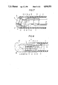
- FIGS. 15 to 17 relate to the eleventh embodiment of the present invention.
- FIG. 15 is a magnified sectioned view of an endoscope tip part.
- FIG. 16 is a sectioned view in the direction of E--E' in FIG. 15.
- FIG. 17 is a sectioned view in the direction of F--F' in FIG. 15.
- FIGS. 1 to 4 relate to the first embodiment of the present invention.
- FIG. 1 is a magnified sectioned view on line B--B' in FIG. 2 showing an industrial endoscope tip part internally fitted with a solid state imaging apparatus.
- FIG. 2 is a magnified sectioned view on line A--A' in FIG. 1.
- FIG. 3 is a schematic perspective view of an endoscope tip part.
- FIG. 4 is an explanatory diagram showing the formation of an essential part.
- the present invention is applied to an industrial endoscope.
- a tip body 1a is formed of a filler, has in the lengthwise direction light guide inserting holes 4 through which are inserted a pair of meniscus-like light guides 6 on both sides of the tip side formed to be flange-like s shown in FIG. 3 and forms on the rear side in the lengthwise direction a pair of light guide incisions 4a communicating with the light guide inserting holes 4.
- a coating sheath 2 made of an insulating material and extended from the rear of the insertable part is fitted and connected to a step formed in the rear of the flange-like tip side.
- a solid state imaging apparatus 3 is embedded with the corners substantially in contact with the outer peripheral part of the tip body 1a within the tip body 1a as held by the above mentioned light guides 6 in FIG. 2.
- An objective lens system 9 formed of a plurality of lenses 7 positioned by an objective frame 10 and spacer 5 is embedded with the optical axis center in the lengthwise direction of the endoscope in front of the above mentioned solid state imaging apparatus 3.
- a cover glass 8 which is also a color filter array is provided adjacently in parallel in the rear of the above mentioned objective system 9.
- a solid state imaging chip 12 die-bonded to a die-bonding pad member 13 formed of a brass plate, for example, gold-plated on both surfaces is arranged adjacently to the above mentioned objective system 9 so as to be substantially at right angles with the lengthwise direction of the endoscope and to have the projected part of the objective system overlapped.
- the material forming the die-bonding pad member 13 may be plastics or ceramics as painted or baked with a conductive paint or plated with a metal.
- the die-bonding pad member 13 is slightly larger than the solid state imaging chip 12. Therefore, even if the position of the solid state imaging chip 12 is somewhat displaced, the solid state imaging chip 12 will not protrude beyond the die-bonding pad member 13 and a reference potential will be given over the entire back surface of the solid state imaging chip.
- the right and left ends and upper end of the die-bonding pad member 13 coincide respectively with the right and left ends and upper end of the cover glass. That is to say, the dimension in the right and left direction of the die-bonding pad member 13 is equal to the dimension in the right and left direction of the cover glass 8.
- an image area 11 of a square, for example, of 2.5 mm. ⁇ 2.5 mm. is formed in the central part except the periphery and chip side bonding pads 15, for example, eight, are provided on one somewhat wide side of the periphery of this image area 11.
- the image area 11 consists of about 30,000 pixels of which the part of 2.5 ⁇ is used.
- a circuit substrate 14 of a thickness, for example, of about 0.3 mm. is provided in the lengthwise direction of the endoscope so as to be in contact with the outer periphery of the tip body 1a, that is, the inner periphery of the coating sheath 2.
- the diameter of the tip body 1a can be made smallest and the small space can be utilized most effectively.
- Conductor patterns are provided on both surfaces of the above mentioned circuit substrate 14, for example, a laminated ceramic condenser 16, chip resistance 17 and cables 18 are fitted to one surface and an IC chip 19 is connected to the other surface through bonding wires 21.
- the above mentioned laminated ceramic condenser 16 is positioned on the front part of the circuit substrate 14.
- One electrode (GND on the circuit) (in a circuit formation in which one electrode 16 is earthed) is electrically and mechanically connected with the above mentioned die-bonding pad member 13.
- the laminated ceramic condenser 16 may not be connected with the die-bonding pad member 13 but may be connected substantially at right angles with the circuit substrate 14 by using the end surface of the die-bonding pad member 13.
- base side bonding pads 22, for example, eight, are provided and are connected through bonding wires 21 with a chip side bonding pads 15 provided on the solid state imaging chip 12.
- the circuit fitted on the circuit substrate 14 is to amplify in the current an output video signal, for example, from the solid state imaging chip 12.
- the end surface in order to increase the smoothness of the end surface, the end surface may be ground and then metalized. Further, in order to minutely form a bonding pad pattern, the end surface may be pattern-printed rather than being so-called side-brazed. Otherwise, a pattern may be formed by laser-trimming after the entire end surface is metalized.
- the solid state imaging chip 12 provided on the circuit substrate 14 has a VDD for an electrode voltage as of an external electrode, V out 1 and V out 2 for the first and second signal outputs, SUB for earthing, ⁇ S 1 and ⁇ S 2 for applying the first and second serial shift clocks, ⁇ P for applying a parallel shift clock, ⁇ T for applying a transfer pulse from the first shift register to the second shift register and ⁇ AB for applying an antiblooming clock which are electrically connected with signal cables 18 through wirings provided on the circuit substrate 14.
- the ⁇ S 1 , ⁇ S 2 , ⁇ P, ⁇ AB, ⁇ T, V out 1 and V out 2 of the above mentioned signal cables 18 are of high frequencies and therefore become noise sources. Therefore, shielding wires are used for their signal lines.
- the VDD and SUB do not become noise sources for the outside and therefore single lines are used for their transmission.
- V out 1 and V out 2 are provided on the circuit substrate 14 and are input into current amplifiers formed in an IC chip 19. That is to say, the V out 1 and V out 2 are applied to the bases of a pair of transistors Q, are electrically amplified and are output from the emitters. The signals output from the respective emitters pass through matching printed resistances r1 and are input into a signal processing circuit not illustrated on the base side. Further, an equivalent resistance r2 provided on the IC chip 19 is connected with the SUB and a dummy is output in the shielding wire as a signal line.
- the laminated ceramic condenser 16 is connected with the VDD, SUB and die-bonding pad member 13.
- the die-bonding pad member 13 is connected with the back surface of the solid state imaging chip 12 and SUB.
- a serial shift clock is to be applied to the ⁇ S1 and ⁇ S2 through a chip resistance 17 for damping.
- the solid state imaging chip 12 to which a driving clock has been applied through the signal cable 18 outputs an observed image formed on the imaging surface as a picture image signal by the photoelectric conversion.
- This picture image signal is amplified by the IC chip 19 forming an amplifying circuit and is delivered to a signal processing circuit not illustrated.
- a composite video signal produced from the picture image signal is output to a monitor not illustrated to display the observed image on the picture surface of the monitor.
- the insertable part tip can be made small in the diameter and can be made short.
- FIGS. 5 and 6 relate to the second embodiment of the present invention.
- FIG. 5 is a magnified sectioned view on line D--D' in FIG. 6 showing a bronchial endoscope tip part internally fitted with a solid state imaging apparatus.
- FIG. 6 is a magnified sectioned view on line C--C' in FIG. 5.
- This embodiment is to apply the present invention to a bronchial endoscope.
- a tip body 1a is formed of a filler in an endoscope tip part 1.
- this tip body 1a formed to be in the form of a flange in the front part, a pair of light guides 6 and a channel 26 for a forceps are inserted parallelly in the lengthwise direction and further a solid state imaging apparatus 3 is embedded in the lengthwise direction.
- curvable frames 27 connected rotatably with each other and made curvable vertically and horizontally are secured in the tip positions and the outer periphery is coated with a coating sheath 2 to be of an outer diameter, for example, of 5.6 mm.
- the tip body 1 is plated or painted with a conductor paint to form a conductive layer on the contact surface with the above mentioned coating sheath which reaches a video processor (camera controlling unit) not illustrated through the curvable frames 27 to develop a shielding effect.
- a video processor camera controlling unit
- an objective system 9 formed of a plurality of lenses 7 positioned by an objective frame 10 and spacer 5 is embedded with the optical axis center in the lengthwise direction of the endoscope.
- a cover glass 8 is provided parallelly adjacently to the rear of the above mentioned objective system 9. Further, in the rear of the cover glass 8, a solid state imaging chip 12 of dimensions, for example, of 1.65 mm. ⁇ 1.4 mm. is arranged adjacently to the above mentioned objective system 9 so as to be substantially at right angles with the lengthwise direction of the endoscope and to have the projection of the objective system 9 overlapped on it.
- the above mentioned solid state imaging chip 12 has an image area 11 of a square of 1 mm. ⁇ 1 mm. and about 10,000 pixels formed in the central part except the periphery.
- Chip side bonding pads 15, for example, five, are provided on one somewhat wider side on the periphery of this image area 11.
- a laminated ceramic condenser 16 and signal cable 18 are fitted to one surface of the above mentioned circuit substrate 14 and the signal cable 18 and an IC chip 19 are fitted to the other surface of the circuit substrate 14.
- the center of the IC chip 19 is provided as displaced in the horizontal direction in FIG. 6 with respect to the circuit substrate 14.
- the above mentioned solid state imaging chip 12 is die-bonding directly with one electrode (GND on the circuit) (in the circuit formation in which one electrode of the laminated ceramic condenser 16 is earthed) of the laminated ceramic condenser 16.
- base side bonding pads 22 for example, five, are provided and are connected with the chip side bonding pads 15 provided on the solid state imaging chip 12 through bonding wires 21.
- the spacing of the base side bonding pads 22 is larger than the spacing of the chip side bonding pads 15, because it is more difficult to provide the base side bonding pads on the end surface of the circuit substrate 14 than to provide the chip side bonding pads 15 on the solid state imaging chip 12.
- an amplifying circuit is formed of this laminated ceramic condenser 16 and IC chip 19.
- the width in the diametral direction of the circuit substrate is provided to be larger than the width of the solid state imaging chip 12 and, as mentioned above, the solid state imaging chip 12 and IC chip 19 are provided eccentrically from the circuit substrate 14. Further, a forceps channel 26 is provided so as to be adjacent to the solid state imaging chip 12, to be in the displaced direction of the circuit substrate 14 with respect to the solid state imaging chip 12 and to be adjacent to the circuit substrate 14.
- each of the solid state imaging chip 12, cover glass 8 and IC chip 19 is 0.5 mm. and the inside diameter of the coating sheath 2 is 4.6 mm.
- the solid state imaging chip 12 to be used is smaller than in the first embodiment, the solid state imaging apparatus 3 is made smaller by directly die-bonding the laminated ceramic condenser and the space through which the forceps channel 26 and light guide 6 can be inserted is secured within the endoscope tip part 1 by providing the solid state imaging chip 12 and IC chip 19 eccentrically with respect to the circuit substrate 14.
- FIG. 7 is a sectioned view of an endoscope tip part having a built-in solid state imaging apparatus of the third embodiment of the present invention.
- the present invention is applied to a front oblique view type endoscope.
- An endoscope tip part 1 is provided with a rigid substantially columnar tip body 1a.
- An observing through hole 31 obliquely upward inclined in the lengthwise direction of the endoscope tip part 1 is provided in the central part of this tip body 1.
- An objective frame 10 in which the objective system 9 is positioned by spacers 5 is fitted and fixed within the observing through hole 31 so as to be exposed in the rear end part out of the tip body 1.
- a solid state imaging chip 12 is overlapped on the rear end surface of the above mentioned objective system 9. Further, a die-bonding pad member 13 having a flange part 32 in the edge part on the oblique view direction side is overlapped on the rear end surface of this solid state imaging chip 12.
- the above mentioned flange part 32 has an angle somewhat larger than a right angle with the jointing plane of the above mentioned solid state imaging chip 12 with the die-bonding pad member 13.
- the plane circuit substrate 14 provided with wirings is jointed with the flange surface 33 forming the flange part 32 so as to be parallel with the lengthwise direction of the endoscope tip part 1.
- a flexible tubular coating sheath 2 is externally fitted and fixed to the rear end part of the above mentioned tip body 1a.
- an IC chip 19 is electrically connected to the circuit substrate 14 by face-bonding which can make the height of the connecting part lower than by wire-bonding.
- the solid state imaging chip 12 and circuit substrate 14 are electrically connected with each other through bonding wires 21.
- a laminated ceramic condenser 16 and chip resistance 17 are provided and electrically connected.
- This circuit substrate 14, laminated ceramic condenser 16 and chip resistance 17 are respectively separately directly soldered with signal cables 18 so as to be able to transmit signals to and from a signal processing circuit not illustrated provided on the base side.
- the solid state imaging chip 12, bonding wire 21, IC chip 19 and a part of the laminated ceramic condenser 16 are sealed with a sealing resin 34.
- the circuit substrate 14 is provided in this space, further the IC chip 19 is connected on the circuit substrate 14 by face-bonding, no flat land for connecting the signal cables 18 is provided on the circuit substrate and the signal cables 18 are soldered directly to the electronic parts, in case the circuit substrate 14 is made short and is provided within the endoscope tip part 1, the outside diameter of the endoscope tip part 1 can be made small and the rigid part can be made short.
- FIG. 8 is a sectioned view of an endoscope tip part having a built-in solid state imaging apparatus of the fourth embodiment of the present invention.
- the present invention is applied to a side view type endoscope.
- An endoscope tip part 1 is provided with a tip body 1a formed to be columnar of such material high in the strength and moistureproofness as an epoxy, polyphenylene sulfide (PPS) or polyimide type resin.
- a solid state imaging apparatus 3 formed of an image forming optical system 36, solid state imaging chip 12, circuit substrate 14 and electronic parts is sealed within the above mentioned tip body 1a.
- an objective 37 forming the image forming optical system 36 is provided with the optical axis at right angles with the lengthwise direction of the endoscope tip part 1.
- a right angular prism 38 is provided so as to make the optical axis of the above mentioned objective 37 parallel with the lengthwise direction of the endoscope tip part 1 and to rearward bend it.
- a circuit substrate 14 is provided so as to be parallel with the lengthwise direction of the endoscope tip part 1 and to be in contact on the front end surface with the rear end surface of the right angular prism 38. Further, an image forming lens frame 40 in which an image forming lens system 39 is positioned by spacers 5 is provided in contact on the front end surface with the rear end surface of the right angular prism 38.
- the imaging surface of the solid state imaging chip 12 is positioned in the image forming position of the above mentioned image forming lens system and near the central part of the circuit substrate 14. This imaging surface side and the circuit substrate 14 are electrically connected with each other through a bonding wire 21 between the solid state imaging chip 12 and the image forming lens system 39. Further, a light transmitting resin 41 is sealed between the solid state imaging chip 12 and the image forming lens system 39.
- a die-bonding pad member 13 formed, for example, of a brass plate gold-plated on both surfaces is provided in the form of a trapezoid as positioned near the middle part of the circuit substrate 14 so as to support the solid state imaging chip 12 from the circuit substrate 14.
- a laminated ceramic condenser 16 and an IC chip are provided on the other surface opposed to the surface on which the solid state imaging chip 12 is provided of the circuit substrate and, in the rear end part, a signal cable 18 transmitting signals is soldered.
- a chip resistance 17 is provided on the rear part of the surface on which the solid state imaging chip 12 is provided.
- a flexible tubular coating tube 2 is externally fitted and fixed to the rear part of the above mentioned tip body 1a.
- the solid state imaging apparatus 3 can be made short and further, as the tip body 1a is formed of only a resin, the outside diameter of the tip part can be made small.
- the right angular prism 38 is provided for the solid state imaging apparatus 3 so as to enable side viewing but any other prism than the right angular prism may be used so as to enable oblique viewing.
- FIG. 9 is a sectioned view of a TV camera having a built-in imaging apparatus of the fifth embodiment of the present invention.
- a solid state imaging apparatus 3 is provided with a rigid cylindrically formed housing 43.
- An objective 44 formed, for example, of a self-convergent type lens is internally fitted and fixed in the front end part within this housing 43.
- a rectangular and, for example, back surface illuminating type solid state imaging chip 46 is provided with the imaging surface in contact with the rear end surface of the objective 44.
- a multilayer substrate 48 formed by laminating, for example, four layers of substrates 47 is provided in the rear of this solid state imaging chip 46 so as to be contained within the projected area in the optical axial direction of the solid state imaging chip 46.
- the substrate 47, for example, in the third layer from below of this multilayer substrate 48 is extended rearward.
- Conductor patterns 49 are provided on the above mentioned respective substrates 47.
- Flat lands 51 provided on the front end surfaces of the respective substrates 47 and the conductor patterns 49 provided on both surfaces of the above mentioned extended substrate 47 are electrically connected with each other.
- This flat land 51 is to be face-bonded with a bump 52 provided on the back surface of the imaging surface of the solid state imaging chip 46.
- An IC chip 19 as an electronic part on one surface of the above mentioned extended substrate 47 and a laminated ceramic condenser 16 on the other surface are respectively face-bonded on the conductor patterns 49.
- Internal wires 54 of a bundled shielding wire 53 as signal cables are soldered to the rear part of the substrate 47 provided with these electronic parts.
- the above mentioned housing 43 is squeezed in the rear part to be small in the diameter and to insert and secure a bundle 56 bundling the above mentioned internal wires 54.
- An integral shielding wire 57 of the bundled shielding wire 53 is soldered to the housing 43 to shield the housing 43.
- This connecting part is reinforced by a reinforcing resin 58 which has a sealing property to keep the interior of the housing 43 air-tight.
- the housing 43 is filled with an inert gas.
- the above mentioned bundled shielding wire 53 is connected to a controlling apparatus having a signal processing circuit not illustrated. Further, the controlling apparatus is to be connected to a monitor not illustrated.
- the multilayer substrate 48 fitted with the electronic parts is provided so as to be substantially at right angles with the solid state imaging chip 46 and to be contained within the projected area of the solid state imaging chip 46 and further the multilayer substrate 48 and solid state imaging chip 46 are face-bonded with each other to make the connecting space small, a three-dimensional high density fitting is made possible, the solid state imaging apparatus 3 can be made small and, therefore, in case the embodiment is used for an endoscope, the endoscope insertable part tip can be made small in the diameter and short.
- FIG. 10 is a sectioned view of a TV camera having a build-in imaging apparatus of the sixth embodiment of the present invention.
- a TV camera 61 is formed of a columnarly formed rigid objective frame 62 and a TV camera body 63 formed of a rigid material and having a built-in solid state imaging apparatus 3.
- an objective system 64 formed of plastic lenses or the like is so positioned as to hold a brightness diaphragm plate 67 with a spacer 5 and step 66.
- the objective frame 62 is made small in the diameter in the rear part and a male screw part 68 is provided in the position of this small diameter.
- a female screw part 69 with which the above mentioned male screw part 68 can be screwed is provided in the front part and a moire removing filter 71 is provided in the rear of the female screw part 69 so that the center line may coincide with the optical axis of the above mentioned objective system 64.
- a solid state imaging chip 12 having a die-bonding pad member 13 secured to the opposite imaging surface side is provided with the imaging surface in contact with the rear end surface of this moire removing filter 71.
- a multilayer ceramic substrate 73 formed by laminating a plurality of ceramic substrates 72 provided parallelly with the lengthwise direction center of the TV camera body 63 is provided with the front end surface in contact with the rear end surface of the above mentioned die-bonding pad member 13.
- This multilayer ceramic substrate 73 is formed, for example, of six layers of ceramic substrates 72 and the third or sixth layer from below is extended rearward.
- the first layer of the above mentioned multilayer ceramic substrate 73 is extended forward and, on its lower surface, a plurality of leads 75 provided with flange parts 74 in the front parts are provided so as to be connected to the internal wirings of the multilayer ceramic substrate 73.
- the above mentioned flange part 74 is electrically connected with a bonding pad part not illustrated of the solid state imaging chip 12 by face-bonding.
- a chip resistance 17 is provided on the lower surface of the ceramic substrate 72 of the third layer of the above mentioned multilayer ceramic substrate 73 and is connected to the internal wirings through bonding wires 21. Further, on the upper surface of the ceramic substrate 72 of the sixth layer, an IC chip 19 is wire-bonded and a laminated ceramic condenser 16 and a connector receiver 76 are respectively face-bonded.
- the above mentioned connected receiver 76 is exposed through the rear end surface of the above mentioned TV camera body 63 so that a connector 82 provided at the end of a signal cable 81 extended from a monitor 79 may be removably connected to the connector receiver 76.
- the interior of the above mentioned TV camera body 63 is sealed with such sealing material 78 high in the elasticity as a silicone type or urethane type bonding agent.
- the electronic parts provided on the multilayer ceramic substrate 73 are to drive the solid state imaging chip 12 and photoelectrically convert an observed image formed on the imaging surface of the solid state imaging chip 12 to produce a picture image signal.
- the picture image signal delivered to the monitor 79 through the connector 82 and signal cable 81 is processed to be converted to such reference video signal, for example, as an NTSC composite signal so that the observed image may be displayed on the picture surface of the monitor 79.
- the TV camera body 63 can be made smallest in the contour.
- FIG. 11 is an explanatory view of a solid state imaging apparatus of the seventh embodiment of the present invention.
- a circuit substrate 14 is a multilayer ceramic substrate 24 formed by laminating, for example, seven layers of ceramic substrates 23 of a thickness of 0.2 mm. each.
- the fourth and fifth layers from below are extended rearward.
- a laminated ceramic condenser 16 and IC chip resistance 17 are fitted to one surface of these extended ceramic substrates 23 and an IC chip 19 is wire-bonded on the opposite surface.
- the first and second layers from below of the multilayer ceramic substrate 24 are extended forward on the front end surface.
- a die-bonding pad member 13 formed, for example, of brass plate gold-plated on both surfaces is secured so as to be in contact with the upper surface of the ceramic substrate 23 of the second layer and the front end surfaces of the third to seventh layers.
- the opposite imaging surface of the solid state imaging chip 12 is bonded to the front end surface of the die-bonding pad member 13. That is to say, the die-bonding pad member 13 is in contact with the second layer of the multilayer ceramic substrate 24.
- Conductor patterns are provided on the contact surface of the above mentioned multilayer ceramic substrate 24 with the solid state imaging chip 12 and on the contact surface of the multilayer ceramic substrate 24 with the die-bonding pad member 13 and are conducted with the die-bonding pad member 13. That is to say, the die-bonding pad member 13 plays a role of an interlayer pattern (through hole) for the circuit substrate 14.
- the multilayer ceramic substrate 24 is likely to lack and become irregular on the sides and corners. Therefore, when the solid state imaging chip 12 is to be directly die-bonded, the entire back surface of the solid state imaging chip 12 will not uniformly contact. Therefore, the die-bonding pad member 13 is provided to improve the adhesion.
- the die-bonding pad member 13, solid state imaging chip 12 and cover glass 8 partly protrude out of the multilayer ceramic substrate 24 as clear from FIG. 11.
- a square image area is formed in the central part except the peripheral side on the above mentioned solid state imaging chip 12.
- a chip side bonding pad not illustrated is provided on a somewhat widened side on the peripheral side of this image area 11.
- a base side bonding pad not illustrated is provided on the front end surface of the first layer of the multilayer ceramic substrate 24 and is connected with the above mentioned chip side bonding pad not illustrated through a bonding wire 21.
- the multilayer ceramic substrate 24 is not on the entire back surface of the die-bonding pad member 13 and is provided with a flat land for a cable 18 on the upper surface of the seventh layer.
- the multilayer ceramic substrate 24 is likely to lack on this side and the other side of the paper surface of the multilayer ceramic substrate 24, if the solid state imaging chip 12 is die-bonded directly to the multilayer ceramic substrate 24 without providing the die-bonding pad member 13, the solid state imaging chip 12 will protrude out of the multilayer ceramic substrate 24 by the lacked part of the multilayer ceramic substrate 24 to be a problem.
- the die-bonding pad member 13 of this embodiment is made of a metal and can be manufactured without producing a lack and therefore such problem is not produced.
- the dimension in the direction vertical to the paper surface of the die-bonding pad member 13 may be made substantially equal to the dimension of the solid state imaging chip 12 the same as in the vertical direction in FIG. 11 and therefore the solid state imaging apparatus 3 can be made small.
- the die-bonding pad member 13 in the direction vertical to the paper surface may protrude out of the multilayer ceramic substrate 24 the same as in the vertical direction in FIG. 11.
- FIG. 12 is a sectioned view of the tip part of a straight view type endoscope containing the imaging apparatus of the eighth embodiment of the present invention.
- An objective system 9 formed of lenses fitted at both ends of a spacer 5 is provided on the tip surface of a tip body 1a provided in the endoscope tip part 1.
- a solid state imaging chip 12 is provided with its imaging surface contacted with the rear end surface of this objective system 9.
- a die-bonding pad member 87 having one edge part forming a flange part 86 bent substantially at right angles is die-bonded on the rear end surface of this solid state imaging chip 12.
- a circuit substrate 14 is secured so as to be extended rearward on one surface from the flange part 86.
- An IC chip 88 is die-bonded to the other surface of the flange part and is connected with the solid state imaging chip 12 by a bonding wire 89 and with the circuit substrate 14 by a bonding wire 91.
- An IC chip 92 is die-bonded to the surface secured to the flange part 86 in the rear of the above mentioned circuit substrate 14 and is connected with the circuit substrate 14 by a bonding wire 93. Further, a laminated ceramic condenser 16 and chip resistance 17 are fitted to the surface not secured to the flange part 86.
- a bump 52 is provided on the rear part of the above mentioned IC chip 92.
- a plurality of leads 100 automatically bonded by tapes to the tip part of a flexible substrate 18 as signal cables are face-bonded to this bump 52.
- Such cooling element 94 as, for example, a Peltier element is provided on the back surface of the bonding pad member 87 to which the above mentioned solid state imaging chip 12 is die-bonded to cool the solid state imaging chip 12 and IC chip 88.
- the dark current of the solid state imaging chip 12 reduces, the S/N ratio improves and a damage by the heating of the IC chip 88 can be prevented.
- the solid state imaging apparatus 3 formed of the objective, solid state imaging chip 12, die-bonding pad member 87 and electronic parts is sealed on the periphery together with a forceps channel tube 97 forming a forceps channel 96 with an epoxy, polyphenylene sulfide (PPS) or polyimide type resin or the like high in the strength and moistureproofness so as to form a tip body 1a which is columnar, is provided with a rounded part 98 on the tip edge and is formed to be somewhat larger in the diameter in the rear part.
- a smaller diameter part is provided by a step and a flexible tubular coating tube 2 is externally fitted to this smaller diameter part.
- a flexible forceps channel tube 99 is externally fitted to the rear part of the above mentioned forceps channel tube 97 and is sealed in the front end part within the tip body 1a.
- the above mentioned rounded part 98 is made to somewhat reach the above mentioned forceps channel 96 on the tip surface of the tip body 1a.
- the input and output signals of the solid state imaging chip 12 are connected to the IC chip 88 through the bonding wire 89.
- one part is processed by the IC chip 88 but the other part passes through the IC chip 88 and is connected with the circuit substrate 14 through the bonding wire 91.
- cooling element 94, laminated ceramic condenser 16 and chip resistance 17 are arranged within the projected area from the imaging surface of the solid state imaging chip 12, the space within the tip body 1a can be three-dimensionally and effectively utilized and the outside diameter of the endoscope tip part 1 can be made smaller.
- FIG. 13 is a sectioned view of a TV camera having a built-in imaging apparatus of the ninth embodiment of the present invention.
- the imaging apparatus of the present invention is applied to a TV camera.
- An observing through hole 102 is provided on the front end surface of a TV camera body 101 formed of a rigid material.
- An objective frame 104 in which an objective system 103 is positioned by a spacer 5 is fitted and fixed in this observing through hole 102.
- This objective system 103 is formed of an infrared ray cutting filter 106, brightness stopping plate 107, image forming lens 108, moire removing filter 109 and color filter array 111 in the mentioned order from the front end surface side.
- a solid state imaging chip 12 is provided in contact on the imaging surface with the rear end surface of the above mentioned color filter array 111, is provided at right angles with the upper surface near the central part of a substrate 112a forming a first circuit substrate 112 provided in parallel with the center line in the lengthwise direction of the TV camera body 101 and is electrically connected with the substrate 112a by a bonding wire 21. Further, on the lower surface of the substrate 112a, a switch 114 which can switch on and off a current source from a battery not illustrated provided within the TV camera body 101 is provided so as to expose the operating part through the TV camera body 101.
- a substrate 112b is provided as overlapped so as to be in contact on the front end surface with the back surface of the solid state imaging chip 12.
- An IC chip 19 and second circuit substrate 113 connected with the substrate 112b by bonding wires 21 are provided from the front on the upper surface of this substrate 112b and further, a printing resistance 116 and electronic part 117 are provided from the front on the lower surface of the substrate 112b.
- the above mentioned second circuit substrate 113 is a multilayer substrate laminated, for example, in four layers. Its rear end surface coincides with the end surface of the above mentioned substrate 112b.
- the substrate of the fourth layer from below extends forward.
- the substrate of the first layer forming the second circuit substrate 113 and the circuit substrate 112b forming the first circuit substrate 112 are electrically connected with each other by the bonding wire 21 on the rear end surfaces.
- Electronic parts 117 and a transmitting element 118 are provided from the front on the upper surface of the substrate of the fourth layer forming the above mentioned second circuit substrate 113. Further, an IC chip 19 wire-bonded with the substrate of the fourth layer is provided on the lower surface of the substrate of the fourth layer.
- the above mentioned transmitting element 118 is provided with a transmitting antenna 119 in the rear so as to extend out of the rear end surface of the TV camera body 101.
- the objective frame 104, switch 114 and transmitting antenna 119 are air-tightly bonded with the TV camera body 101 which is filled with an inert gas.
- the observed image formed on the imaging surface of the solid state imaging chip 12 is photoelectrically converted, is output as an image signal and is processed to produce a so-called composite video signal including a synchronous signal, for example, of an NTSC system.
- this composite video signal is converted to such high frequency wave as of a UHF band by the transmitting element 118 formed, for example, of an RF modulator and is transmitted as an electric wave from the transmitting antenna 119.
- This electric wave is received by an antenna, for example, of an ordinary television receiver not illustrated and is demodulated by this television receiver and the observed image of this television receiver is displayed.
- the TV camera body 101 can be made smallest in the contour, is made wireless and therefore can be improved in the handlability.
- FIG. 14 is an explanatory view of an imaging apparatus of the tenth embodiment of the present invention.
- An imaging apparatus 3 is contained within a housing 121 formed to be substantially columnar.
- This housing 121 is formed of such light transmitting resin as, for example, plastics, has a smooth convex spherical surface by a radius of curvature on the front end surface and is provided with a recess 122 on the rear end surface.
- a solid state imaging chip 46 for example, of a back surface illuminating type is embedded with the imaging surface directed forward, with the center of the imaging surface coinciding with the center line of the rotation of the housing 121 and further with the opposite imaging surface of the solid state imaging chip 46 exposed within the recess.
- a cylindrical light intercepting tube 124 is provided with the rear end surface in contact with the imaging surface of the above mentioned solid state imaging chip 46.
- a hollow part 126 is formed within the light intercepting tube 124.
- the front end surface of this hollow part 126, that is, the housing 121 is formed to be a rearward convex smooth spherical surface by a radius of curvature and is to form a two-surface nonspherical lens together with the convex spherical surface formed on the front end surface of the above mentioned housing 121.
- a circuit substrate 14 is provided in parallel with the center line of the rotation of the housing 121 in the rear of the above mentioned solid state imaging chip 46.
- the front end surface of this circuit substrate 14 and the opposite imaging surface of the solid state imaging chip 46 are face-bonded with each other by a bump 52.
- the end surface of an electronic part 127 is provided to coincide with the front end surface of the circuit substrate 14 and is face-bonded to the opposite imaging surface of the solid state imaging chip 46 through a bump 52 the same as of the circuit substrate 14.
- a transmitter-receiver 128 having such electromotive force generating means as a solar battery and such laser generating means as a semiconductor laser is provided as connected with an optical fiber cable 129 as signal lines having transmitting courses of the two systems. Also, IC chips 19 are respectively face-bonded on the lower surface of the circuit substrate 14.
- optical fiber cable 129 is connected at the tip to a controlling apparatus not illustrated having a photoelectric converting circuit and an electric power feeding laser generating means.
- the above mentioned circuit substrate 14, IC chips 19, electronic part 127 and transmitter-receiver 128 are made to be contained within the projected area in the optical axial direction of the solid state imaging chip 46. Further, the above mentioned circuit substrate 14, IC chips 19, electronic part 127, transmitter-receiver 128 and optical fiber cable 129 in the front end part are made to be contained within the above mentioned recess 122. The space within this recess 122 is filled with such sealing material 131 settable by ultraviolet rays as, for example, a photosetting resin to seal the contained electronic parts.
- the laser light emitted from the electric power feeding laser generating means provided within the controlling apparatus not illustrated is transmitted through one course of the optical fiber cable 129, is input into the transmitter-receiver 128, is received by the solar battery and is converted to an electric power to be able to be fed to the respective electronic parts forming the solid state imaging apparatus 3.
- the electronic part 127 forming a driver circuit fed with the electric power as mentioned above delivers a driving clock to the solid state imaging chip 12.
- the observed image formed on the imaging surface of the solid state imaging chip 12 is photoelectrically converted and is output as a picture image signal.
- This picture image signal is processed to produce a composite video signal.
- the luminous intensity of the semiconductor laser provided in the transmitter-receiver 128 is directly modulated by this composite video signal and a video information signal is delivered to the other course of the optical fiber cable 129 and is converted to a composite video signal by a photoelectrically converting circuit not illustrated to display the observed image in a monitor not illustrated.
- the modulating system may encode the pulses of the semiconductor laser by the FM modulation, PFM modulation or PWM modulation.
- the housing also a lens
- the number of parts can be reduced and the outside diameter of the solid state imaging apparatus 3 can be made smaller.
- the electronic parts are sealed with a photosetting resin, the producing process can be simplified.
- FIGS. 15 to 17 relate to the eleventh embodiment of the present invention.
- FIG. 15 is a magnified sectioned view of an endoscope tip part.
- FIG. 16 is a sectioned view in the direction E--E' in FIG. 15.
- FIG. 17 is a sectioned view in the direction F--F' in FIG. 16.
- the tip part 137 of an endoscope insertable part 136 is provided with a substantially columnar tip forming member 138 made of such rigid material as, for example, a metal.
- An observing through hole 139 passing parallelly in the lengthwise direction through the above mentioned insertable part 136 and forceps channel through hole 141 and an illuminating through hole and air and water feeding channel through hole not illustrated are formed in the above mentioned tip forming member 138.
- the tip forming member 138 may be of a plastic molding, ceramic molding or metal die-casting and is preferably insulative. In using a conductive material, it is preferable to apply an insulating coating on the outer periphery.
- An objective frame 144 is fitted in the above mentioned observing through hole 139 and is positioned by a positioning pin 145.
- an objective system 146 and circular second cover glass 147 are positioned by a step 148 of the objection frame 144 and a spacer 149 and are fitted. By the way, the focus is adjusted by varying the thickness of the spacer 149.
- such chip supporting frame 151 as, for example, a shielding film is inserted and fixed and a solid state imaging chip 152 arranged so as to have the imaging surface positioned in the image forming position of the above mentioned objective system 146 is held by the above mentioned chip supporting frame 151.
- the objective frame 144 and chip supporting frame 151 are electrically connected with each other.
- a square first cover glass 153 which is also a color filter array wherein color filters respectively transmitting three primary colors, for example, of red(R), green(G) and blue(B) are arranged in the form of a mosaic or the like is provided as overlapped and is bonded so that the light path center of the above mentioned optical system 146 may coincide.
- six bonding pads 154 on the chip side are provided on one somewhat widened side on the periphery of the image area.
- Such circuit substrate 156 as, for example, a multilayer ceramic substrate on which such electronic part 155 as, for example, a CCD driving circuit is fitted as in FIG. 17 is arranged within the above mentioned chip supporting frame 151.
- a die-bonding pad member 157 made, for example, of a metal is mechanically and electrically connected substantially at right angles with the circuit substrate 156 on the front end part of the above mentioned circuit substrate 156.
- the above mentioned solid state imaging chip 152 is die-bonded to the front surface of the above mentioned die-bonding pad member 157.
- a cable fixing member 163 holding such signal cable 162 as, for example, a shielding wire inserted through the above mentioned insertable part 136 is mechanically and electrically connected substantially at right angles with the circuit substrate 156 and the signal cable 162 passing through the above mentioned cable fixing member 163 is connected to the circuit substrate 156.
- the space within the chip supporting frame 151 is filled with such sealing member 161 as, for example, an epoxy resin.
- a forceps channel connecting pipe 164 is fitted to the rear end side of the above mentioned forceps channel through hole 141 and is expanded in the diameter in the rear end part to which a forceps channel tube 160 forming a forceps channel 166 is connected as inserted through the insertable part 136.
- a light distributing lens system not illustrated is fitted in an illuminating through hole not illustrated and a light guide 168 coated with a tube 167 is connected to the rear end of this light distributing lens system as shown in FIG. 16.
- An air and water feeding nozzle not illustrated is fitted to an air and water feeding channel through hole not illustrated and is connected with an air and water feeding tube 171 forming an air and water feeding channel 169 as shown in FIG. 16.
- two above mentioned light guides 168 and one air and water feeding channel 169 are provided.
- three extended parts 175a, 175b and 175c are provided near the outer periphery of the chip supporting frame 151 to protect it and the upper and lower extended parts 175a and 175c are provided respectively with steps 178a and 178c fitting later described protective members 172.
- the extended parts 175a, 175b, and 175c may be connected with the adjacent extended parts 175a, 175b and 175c.
- substantially annular articulating frames 174 are rotatably connected in the lengthwise direction in a curvable part 173 adjacent to the rear of the above mentioned tip part 137.
- the foremost articulating frame 174 is rotatably connected to a curving shaft 177 provided in the rear end part of the later described protective member 172.
- the above mentioned protective member 172 is substantially annular, is provided with a first incision 170a in the position corresponding to the above mentioned extended parts 175a and 175c and with a second incision 170b near the connecting part of the forceps channel tube 160 with the forceps channel connecting pipe 164 inserted in the forceps channel through hole 141, is externally fitted to the rear end part of the above mentioned tip forming member 138 and is fixed with a fixing screw 165.
- the above mentioned articulating frame 174 is contained within a blade 179 knit in the form of a net of such fine wires as of a metal.
- the above mentioned tip part 137 and curvable part 173 are coated with a coating tube 176 as an outer coating.
- the tip part of this coating tube 176 is externally fitted to the above mentioned tip forming member 138, is wound, for example, with a thread and is then fixed with a bonding agent.
- the objective frame 144 arranged in the tip part forming member 138 and the chip supporting frame 151 containing the solid state imaging chip 152, circuit substrate 156 and cable fixing member 163 are protected by the extended parts 175a, 175b and 175c and the light guide 168 and air and water feeding channel 169 are protected by the protective member 172.
- the protective member 172 For such part in which the contents themselves have a strength as the forceps channel connecting pipe 164, as the protective member 172 is incised, the space within the tip part 137 is effectively used and the diameter can be made smaller by the thickness of the protective member 172.
- the entire periphery is to be protected by only the tip forming member instead of the conventional protective member, the contents will not be able to be incorporated in the tip forming member.
- the extended parts may be made only in a part and the other parts may be left open and then covered with the protective member after the contents are incorporated.
- the solid state imaging apparatus according to the present invention is used for endoscopes and TV cameras.
- the present invention is not restricted to be used only for endoscopes for TV cameras, can be used as an imaging means for electronic still cameras and the like and is effective to make the size smaller.
Abstract
Description
Claims (12)
Applications Claiming Priority (4)
| Application Number | Priority Date | Filing Date | Title |
|---|---|---|---|
| JP1101387 | 1987-01-20 | ||
| JP62-11013 | 1987-01-20 | ||
| JP62-44481 | 1987-02-27 | ||
| JP62044481A JPH074338B2 (en) | 1987-02-27 | 1987-02-27 | Endoscope |
Publications (1)
| Publication Number | Publication Date |
|---|---|
| US4918521A true US4918521A (en) | 1990-04-17 |
Family
ID=26346378
Family Applications (1)
| Application Number | Title | Priority Date | Filing Date |
|---|---|---|---|
| US07/143,995 Expired - Lifetime US4918521A (en) | 1987-01-20 | 1988-01-14 | Solid state imaging apparatus |
Country Status (1)
| Country | Link |
|---|---|
| US (1) | US4918521A (en) |
Cited By (123)
| Publication number | Priority date | Publication date | Assignee | Title |
|---|---|---|---|---|
| US5050584A (en) * | 1989-09-22 | 1991-09-24 | Olympus Optical Co., Ltd. | Endoscope with a solid-state image pickup device |
| US5121213A (en) * | 1987-02-25 | 1992-06-09 | Olympus Optical Co., Ltd. | Imaging system having a blurring optical element for minimizing moire phenomenon |
| EP0492349A1 (en) * | 1990-12-28 | 1992-07-01 | Matsushita Electric Industrial Co., Ltd. | Camera head for solid-state image pickup device and method of producing same |
| US5130804A (en) * | 1990-01-09 | 1992-07-14 | Konica Corporation | Compact recording apparatus with functional components mounted on a substrate |
| DE4211857A1 (en) * | 1991-04-11 | 1992-10-15 | Yugengaisha Wai Kei Kikaku | Multi-unit CCD TV camera with head unit coupled over long cable to base - uses head unit processing circuit to provide video signals handled by differential coil transmitting unit connected to cable |
| EP0515085A2 (en) * | 1991-05-20 | 1992-11-25 | Matsushita Electric Industrial Co., Ltd. | Cable connecting structure of a solid state image sensor |
| DE4129961A1 (en) * | 1991-09-10 | 1993-03-18 | Wolf Gmbh Richard | VIDEO ENDOSCOPE WITH FIXED BODY IMAGING DEVICE |
| US5228430A (en) * | 1989-08-04 | 1993-07-20 | Kabushiki Kaisha Toshiba | Electronic endoscope apparatus including easy focusing distal end |
| US5255667A (en) * | 1990-09-12 | 1993-10-26 | Kabushiki Kaisha Toshiba | Endoscope with compact scope end section |
| US5270534A (en) * | 1992-09-14 | 1993-12-14 | U.S. Philips Corporation | Solid-state image recording apparatus having two pairs of adjustment members |
| EP0587513A2 (en) * | 1992-09-11 | 1994-03-16 | Welch Allyn, Inc. | Replaceable lens assembly for video laparoscope |
| DE4319938C1 (en) * | 1993-06-16 | 1994-12-08 | Siemens Ag | Retaining device for a semiconductor scanner (video scanner, image sensor) |
| US5406477A (en) * | 1991-08-30 | 1995-04-11 | Digital Equipment Corporation | Multiple reasoning and result reconciliation for enterprise analysis |
| WO1995015060A1 (en) * | 1993-11-22 | 1995-06-01 | Apollo Camera, L.L.C. | Single sensor video imaging system and method using sequential color object illumination |
| US5454366A (en) * | 1990-11-27 | 1995-10-03 | Asashi Kogaku Kogyo Kabushiki Kaisha | Endoscope distal end with folded circuit board |
| US5575757A (en) * | 1992-10-09 | 1996-11-19 | Smith & Nephew Endoscopy Inc. | Endoscope with focusing mechanism |
| WO1996036294A1 (en) | 1995-05-19 | 1996-11-21 | Cooper David H | Modular intra-oral imaging system video camera |
| EP0745347A2 (en) * | 1995-05-31 | 1996-12-04 | Machida Endoscope Co., Ltd | Endoscope |
| US5594497A (en) * | 1993-04-07 | 1997-01-14 | Ahern; John M. | Endoscope provided with a distally located color CCD |
| US5609561A (en) * | 1992-06-09 | 1997-03-11 | Olympus Optical Co., Ltd | Electronic type endoscope in which image pickup unit is dismounted to execute disinfection/sterilization processing |
| US5653677A (en) * | 1994-04-12 | 1997-08-05 | Fuji Photo Optical Co. Ltd | Electronic endoscope apparatus with imaging unit separable therefrom |
| US5696553A (en) * | 1992-09-25 | 1997-12-09 | Bristol-Myers Squibb Co. | Remote imager video camera cable compensation circuitry |
| US5734418A (en) * | 1996-07-17 | 1998-03-31 | Welch Allyn, Inc. | Endoscope with tab imager package |
| US5754313A (en) * | 1996-07-17 | 1998-05-19 | Welch Allyn, Inc. | Imager assembly |
| US5760452A (en) * | 1991-08-22 | 1998-06-02 | Nec Corporation | Semiconductor memory and method of fabricating the same |
| US5800344A (en) * | 1996-10-23 | 1998-09-01 | Welch Allyn, Inc. | Video laryngoscope |
| US5857963A (en) * | 1996-07-17 | 1999-01-12 | Welch Allyn, Inc. | Tab imager assembly for use in an endoscope |
| EP0941691A1 (en) | 1998-03-11 | 1999-09-15 | Welch Allyn, Inc. | Compact video imaging assembly |
| US6086528A (en) * | 1997-09-11 | 2000-07-11 | Adair; Edwin L. | Surgical devices with removable imaging capability and methods of employing same |
| US6095970A (en) * | 1997-02-19 | 2000-08-01 | Asahi Kogaku Kogyo Kabushiki Kaisha | Endoscope |
| US6141037A (en) * | 1998-03-18 | 2000-10-31 | Linvatec Corporation | Video camera system and related method |
| US6206825B1 (en) * | 1995-06-29 | 2001-03-27 | Olympus Optical Co., Ltd. | Illumination system for endoscopes and an endoscope having the illumination system |
| US6417885B1 (en) * | 1995-08-30 | 2002-07-09 | Matsushita Electric Industrial Co., Ltd. | Solid-state image pickup device with a separable circuit board |
| US6449006B1 (en) * | 1992-06-26 | 2002-09-10 | Apollo Camera, Llc | LED illumination system for endoscopic cameras |
| US20020193663A1 (en) * | 2001-06-13 | 2002-12-19 | Olympus Optical Co., Ltd. | Electronic endoscope |
| US6498884B1 (en) | 1999-10-21 | 2002-12-24 | Quickie Vision Llc | Wide-view endoscope compatible with HDTV format |
| US6567115B1 (en) * | 1999-01-07 | 2003-05-20 | Sony Corporation | Solid-state imaging device |
| US20030171649A1 (en) * | 2002-03-08 | 2003-09-11 | Takeshi Yokoi | Capsule endoscope |
| US20030194793A1 (en) * | 1997-03-31 | 2003-10-16 | Genentech, Inc. | Secreted and transmembrane polypeptides and nucleic acids encoding the same |
| US6652452B1 (en) | 1999-10-25 | 2003-11-25 | Advanced Medical Electronics Corporation | Infrared endoscope with sensor array at the distal tip |
| US6659940B2 (en) * | 2000-04-10 | 2003-12-09 | C2Cure Inc. | Image sensor and an endoscope using the same |
| US20030233024A1 (en) * | 2002-06-14 | 2003-12-18 | Fuji Photo Optical Co., Ltd. | Electronic endoscope for stereoscopic endoscope system |
| US6767322B1 (en) * | 1999-06-08 | 2004-07-27 | Olympus Corporation | Endoscope device |
| EP1441252A1 (en) * | 2001-11-30 | 2004-07-28 | West Electric Co., Ltd. | Strobe apparatus and its manufacturing method |
| US6840903B2 (en) | 2002-03-21 | 2005-01-11 | Nuvista Technology Corporation | Laryngoscope with image sensor |
| US20050192477A1 (en) * | 2004-02-26 | 2005-09-01 | Olympus Winter & Ibe Gmbh | Rigid endoscope optics with a compound housing |
| WO2005086473A1 (en) * | 2004-03-03 | 2005-09-15 | Robert Bosch Gmbh | Camera |
| US6970486B2 (en) * | 2000-05-19 | 2005-11-29 | Rohm Co., Ltd. | Mold type semiconductor laser |
| US20060069305A1 (en) * | 2004-09-30 | 2006-03-30 | Boston Scientific Scimed, Inc. | Device with enhanced indication of use and prevention of re-use |
| US20060167341A1 (en) * | 2005-01-25 | 2006-07-27 | Fujinon Corporation | Endoscope |
| EP1705900A1 (en) * | 2005-03-22 | 2006-09-27 | MEKRA Lang GmbH & Co. KG | Outdoor camera |
| US20060235274A1 (en) * | 2004-02-26 | 2006-10-19 | Olympus Winter & Ibe Gmbh | Rigid endoscope optics with a compound housing |
| US20060264708A1 (en) * | 2005-05-20 | 2006-11-23 | Karl Storz Endovision | Liner for endoscope working channel |
| US7170677B1 (en) | 2002-01-25 | 2007-01-30 | Everest Vit | Stereo-measurement borescope with 3-D viewing |
| EP1793589A1 (en) * | 2005-11-30 | 2007-06-06 | Mitsumi Electric Co., Ltd. | Camera module |
| US7241263B2 (en) | 2004-09-30 | 2007-07-10 | Scimed Life Systems, Inc. | Selectively rotatable shaft coupler |
| US20070179342A1 (en) * | 2006-01-12 | 2007-08-02 | Kb Port Llc | Wireless Laryngoscope with Internal Antennae and One Piece Construction Adapted for Laryngoscopy Training |
| US20070182843A1 (en) * | 2006-02-03 | 2007-08-09 | Fujifilm Corporation | Solid-state imaging device and electronic endoscope using the same |
| EP1925252A1 (en) * | 2005-09-14 | 2008-05-28 | Olympus Corporation | Tip structure part of endoscope |
| US20080200757A1 (en) * | 2001-06-28 | 2008-08-21 | Arkady Glukhovsky | Vivo imaging device with a small cross sectional area and methods for construction thereof |
| US20080277673A1 (en) * | 2007-05-10 | 2008-11-13 | Stmicroelectronics S.A. | Cavity exploration with an image sensor |
| US20100261961A1 (en) * | 2006-12-21 | 2010-10-14 | Intuitive Surgical Operations, Inc. | Hermetically sealed distal sensor endoscope |
| US20100283854A1 (en) * | 2008-05-12 | 2010-11-11 | Flir Systems, Inc. | Optical Payload Electrical System |
| US7846107B2 (en) | 2005-05-13 | 2010-12-07 | Boston Scientific Scimed, Inc. | Endoscopic apparatus with integrated multiple biopsy device |
| US7955255B2 (en) | 2006-04-20 | 2011-06-07 | Boston Scientific Scimed, Inc. | Imaging assembly with transparent distal cap |
| US7967759B2 (en) | 2006-01-19 | 2011-06-28 | Boston Scientific Scimed, Inc. | Endoscopic system with integrated patient respiratory status indicator |
| US20110237886A1 (en) * | 2010-03-26 | 2011-09-29 | Fujifilm Corporation | Imaging unit and endoscope |
| US8052597B2 (en) | 2005-08-30 | 2011-11-08 | Boston Scientific Scimed, Inc. | Method for forming an endoscope articulation joint |
| US20110288372A1 (en) * | 2008-12-10 | 2011-11-24 | Lasse Kjeld Gjoeske Petersen | Endoscope having a camera housing and method for making a camera housing |
| US8083671B2 (en) | 2004-09-30 | 2011-12-27 | Boston Scientific Scimed, Inc. | Fluid delivery system for use with an endoscope |
| US8097003B2 (en) | 2005-05-13 | 2012-01-17 | Boston Scientific Scimed, Inc. | Endoscopic apparatus with integrated variceal ligation device |
| US8118732B2 (en) | 2003-04-01 | 2012-02-21 | Boston Scientific Scimed, Inc. | Force feedback control system for video endoscope |
| US8199187B2 (en) | 2004-09-30 | 2012-06-12 | Boston Scientific Scimed, Inc. | Adapter for use with digital imaging medical device |
| US8202265B2 (en) | 2006-04-20 | 2012-06-19 | Boston Scientific Scimed, Inc. | Multiple lumen assembly for use in endoscopes or other medical devices |
| US8213676B2 (en) | 2006-12-20 | 2012-07-03 | Ge Inspection Technologies Lp | Inspection apparatus method and apparatus comprising motion responsive control |
| US8353860B2 (en) | 2004-09-30 | 2013-01-15 | Boston Scientific Scimed, Inc. | Device for obstruction removal with specific tip structure |
| US8357148B2 (en) | 2004-09-30 | 2013-01-22 | Boston Scientific Scimed, Inc. | Multi-functional endoscopic system for use in electrosurgical applications |
| US8425408B2 (en) | 2003-04-01 | 2013-04-23 | Boston Scientific Scimed, Inc. | Articulation joint for video endoscope |
| US8435172B2 (en) | 2004-09-30 | 2013-05-07 | Boston Scientific Scimed, Inc. | Automated control of irrigation and aspiration in a single-use endoscope |
| US8475366B2 (en) | 2003-04-01 | 2013-07-02 | Boston Scientific Scimed, Inc. | Articulation joint for a medical device |
| US8535219B2 (en) | 2003-04-01 | 2013-09-17 | Boston Scientific Scimed, Inc. | Fluid manifold for endoscope system |
| US20140003018A1 (en) * | 2011-03-04 | 2014-01-02 | Olympus Corporation | Wiring board, manufacturing method for wiring board, and image pickup apparatus |
| US8622894B2 (en) | 2003-04-01 | 2014-01-07 | Boston Scientific Scimed, Inc. | Articulation joint |
| US20140042578A1 (en) * | 1996-05-17 | 2014-02-13 | Sony Corporation | Solid-state imaging apparatus and camera using the same |
| US8810636B2 (en) | 2006-12-20 | 2014-08-19 | Ge Inspection Technologies, Lp | Inspection apparatus method and apparatus comprising selective frame output |
| US8888684B2 (en) | 2006-03-27 | 2014-11-18 | Boston Scientific Scimed, Inc. | Medical devices with local drug delivery capabilities |
| EP2818094A1 (en) * | 2013-06-17 | 2014-12-31 | Karl Storz GmbH & Co. KG | Observation instrument with a symmetrical field of view using asymmetric image sensors |
| US8952312B2 (en) | 2011-05-12 | 2015-02-10 | Olive Medical Corporation | Image sensor for endoscopic use |
| US20150065800A1 (en) * | 2012-05-18 | 2015-03-05 | Olympus Winter & Ibe Gmbh | Video endoscope |
| US20150109504A1 (en) * | 2013-10-22 | 2015-04-23 | Canon Kabushiki Kaisha | Image capturing apparatus, solid-state image sensor, and camera |
| US20150190039A1 (en) * | 2013-06-28 | 2015-07-09 | Olympus Medical Systems Corp. | Imaging module and endoscope device |
| US9462234B2 (en) | 2012-07-26 | 2016-10-04 | DePuy Synthes Products, Inc. | Camera system with minimal area monolithic CMOS image sensor |
| US20160307954A1 (en) * | 2013-12-27 | 2016-10-20 | Nikon Corporation | Image-capturing unit and image-capturing apparatus |
| US9516239B2 (en) | 2012-07-26 | 2016-12-06 | DePuy Synthes Products, Inc. | YCBCR pulsed illumination scheme in a light deficient environment |
| US9622651B2 (en) | 2012-01-27 | 2017-04-18 | Kbport Llc | Wireless laryngoscope simulator with onboard event recording adapted for laryngoscopy training |
| US9641815B2 (en) | 2013-03-15 | 2017-05-02 | DePuy Synthes Products, Inc. | Super resolution and color motion artifact correction in a pulsed color imaging system |
| US9777913B2 (en) | 2013-03-15 | 2017-10-03 | DePuy Synthes Products, Inc. | Controlling the integral light energy of a laser pulse |
| US20170365963A1 (en) * | 2016-06-20 | 2017-12-21 | Sumitomo Electric Industries, Ltd. | Coaxial cable and method for manufacturing the same |
| EP2498667A4 (en) * | 2009-11-13 | 2017-12-27 | California Institute of Technology | Stereo imaging miniature endoscope with single imaging chip and conjugated multi-bandpass filters |
| US10084944B2 (en) | 2014-03-21 | 2018-09-25 | DePuy Synthes Products, Inc. | Card edge connector for an imaging sensor |
| US10091406B2 (en) * | 2016-03-14 | 2018-10-02 | Lg Electronics Inc. | Image capturing apparatus |
| US20180296076A1 (en) * | 2015-10-27 | 2018-10-18 | Olympus Corporation | Imageing device and endoscope |
| US10251530B2 (en) | 2013-03-15 | 2019-04-09 | DePuy Synthes Products, Inc. | Scope sensing in a light controlled environment |
| US10278568B2 (en) | 2007-12-18 | 2019-05-07 | Harish M. MANOHARA | Endoscope and system and method of operation thereof |
| US10291850B2 (en) | 2006-12-20 | 2019-05-14 | General Electric Company | Inspection apparatus method and apparatus comprising selective frame output |
| US10321804B2 (en) | 2013-01-07 | 2019-06-18 | Ambu A/S | Articulated tip part for an endoscope |
| US10517469B2 (en) | 2013-03-15 | 2019-12-31 | DePuy Synthes Products, Inc. | Image sensor synchronization without input clock and data transmission clock |
| US10561302B2 (en) | 2013-03-15 | 2020-02-18 | DePuy Synthes Products, Inc. | Viewing trocar with integrated prism for use with angled endoscope |
| US10568496B2 (en) | 2012-07-26 | 2020-02-25 | DePuy Synthes Products, Inc. | Continuous video in a light deficient environment |
| US10750933B2 (en) | 2013-03-15 | 2020-08-25 | DePuy Synthes Products, Inc. | Minimize image sensor I/O and conductor counts in endoscope applications |
| US20210275006A1 (en) * | 2016-12-06 | 2021-09-09 | Haesung Optics | Micro endoscope camera module and micro endoscope having same |
| US20210330175A1 (en) * | 2020-04-27 | 2021-10-28 | Schölly Fiberoptic GmbH | Flexible endoscope based upon an investment composition |
| US11323598B2 (en) | 2018-01-09 | 2022-05-03 | Olympus Corporation | Image pickup apparatus, method of manufacturing image pickup apparatus, and endoscope |
| US11330972B2 (en) * | 2018-01-11 | 2022-05-17 | Olympus Corporation | Oblique-viewing endoscope |
| US11357392B2 (en) | 2017-06-26 | 2022-06-14 | Ambu A/S | Bending section for an endoscope |
| US11382496B2 (en) | 2006-12-21 | 2022-07-12 | Intuitive Surgical Operations, Inc. | Stereoscopic endoscope |
| US20220352233A1 (en) * | 2020-01-22 | 2022-11-03 | Olympus Corporation | Image pickup apparatus, endoscope, and method of manufacturing image pickup apparatus |
| US11672413B2 (en) | 2017-03-24 | 2023-06-13 | Ambu A/S | Articulated tip part for an endoscope |
| US11766163B2 (en) | 2019-09-26 | 2023-09-26 | Ambu A/S | Tip part for an endoscope and the manufacture thereof |
| US11819185B2 (en) | 2020-04-27 | 2023-11-21 | Scholly Fiberoptic Gmbh | Flexible endoscope with skeleton structure |
| US11887502B2 (en) | 2018-01-04 | 2024-01-30 | Applied Medical Resources Corporation | Surgical simulation camera scope |
| US11937781B2 (en) | 2020-06-19 | 2024-03-26 | Ambu A/S | Endoscope comprising an articulated bending section body |
| US11955498B2 (en) * | 2022-07-14 | 2024-04-09 | Olympus Corporation | Image pickup apparatus, endoscope, and method of manufacturing image pickup apparatus |
Citations (10)
| Publication number | Priority date | Publication date | Assignee | Title |
|---|---|---|---|---|
| US4491865A (en) * | 1982-09-29 | 1985-01-01 | Welch Allyn, Inc. | Image sensor assembly |
| US4573450A (en) * | 1983-11-11 | 1986-03-04 | Fuji Photo Optical Co., Ltd. | Endoscope |
| US4575805A (en) * | 1980-12-24 | 1986-03-11 | Moermann Werner H | Method and apparatus for the fabrication of custom-shaped implants |
| JPS61163315A (en) * | 1985-01-14 | 1986-07-24 | Olympus Optical Co Ltd | Endoscope |
| US4651202A (en) * | 1984-05-16 | 1987-03-17 | Fuji Photo Optical Co., Ltd. | Video endoscope system |
| US4677471A (en) * | 1985-08-16 | 1987-06-30 | Olympus Optical Co., Ltd. | Endoscope |
| US4682219A (en) * | 1985-08-16 | 1987-07-21 | Fuji Photo Optical Co., Ltd. | Endoscope |
| US4692608A (en) * | 1984-05-18 | 1987-09-08 | Fuji Photo Optical Company, Ltd. | Compact optical imaging system |
| US4745470A (en) * | 1986-04-04 | 1988-05-17 | Olympus Optical Co., Ltd. | Endoscope using a chip carrier type solid state imaging device |
| US4757805A (en) * | 1986-06-25 | 1988-07-19 | Olympus Optical Co., Ltd. | Endoscope |
-
1988
- 1988-01-14 US US07/143,995 patent/US4918521A/en not_active Expired - Lifetime
Patent Citations (10)
| Publication number | Priority date | Publication date | Assignee | Title |
|---|---|---|---|---|
| US4575805A (en) * | 1980-12-24 | 1986-03-11 | Moermann Werner H | Method and apparatus for the fabrication of custom-shaped implants |
| US4491865A (en) * | 1982-09-29 | 1985-01-01 | Welch Allyn, Inc. | Image sensor assembly |
| US4573450A (en) * | 1983-11-11 | 1986-03-04 | Fuji Photo Optical Co., Ltd. | Endoscope |
| US4651202A (en) * | 1984-05-16 | 1987-03-17 | Fuji Photo Optical Co., Ltd. | Video endoscope system |
| US4692608A (en) * | 1984-05-18 | 1987-09-08 | Fuji Photo Optical Company, Ltd. | Compact optical imaging system |
| JPS61163315A (en) * | 1985-01-14 | 1986-07-24 | Olympus Optical Co Ltd | Endoscope |
| US4677471A (en) * | 1985-08-16 | 1987-06-30 | Olympus Optical Co., Ltd. | Endoscope |
| US4682219A (en) * | 1985-08-16 | 1987-07-21 | Fuji Photo Optical Co., Ltd. | Endoscope |
| US4745470A (en) * | 1986-04-04 | 1988-05-17 | Olympus Optical Co., Ltd. | Endoscope using a chip carrier type solid state imaging device |
| US4757805A (en) * | 1986-06-25 | 1988-07-19 | Olympus Optical Co., Ltd. | Endoscope |
Cited By (232)
| Publication number | Priority date | Publication date | Assignee | Title |
|---|---|---|---|---|
| US5121213A (en) * | 1987-02-25 | 1992-06-09 | Olympus Optical Co., Ltd. | Imaging system having a blurring optical element for minimizing moire phenomenon |
| US5450243A (en) * | 1987-02-25 | 1995-09-12 | Olympus Optical Co., Ltd. | Imaging system having a blurring optical element for minimizing moire phenomenon |
| US5228430A (en) * | 1989-08-04 | 1993-07-20 | Kabushiki Kaisha Toshiba | Electronic endoscope apparatus including easy focusing distal end |
| US5050584A (en) * | 1989-09-22 | 1991-09-24 | Olympus Optical Co., Ltd. | Endoscope with a solid-state image pickup device |
| US5130804A (en) * | 1990-01-09 | 1992-07-14 | Konica Corporation | Compact recording apparatus with functional components mounted on a substrate |
| US5255667A (en) * | 1990-09-12 | 1993-10-26 | Kabushiki Kaisha Toshiba | Endoscope with compact scope end section |
| US5454366A (en) * | 1990-11-27 | 1995-10-03 | Asashi Kogaku Kogyo Kabushiki Kaisha | Endoscope distal end with folded circuit board |
| EP0492349A1 (en) * | 1990-12-28 | 1992-07-01 | Matsushita Electric Industrial Co., Ltd. | Camera head for solid-state image pickup device and method of producing same |
| US5233426A (en) * | 1990-12-28 | 1993-08-03 | Matsushita Electric Industrial Co., Ltd. | Reduced diameter camera head for solid-state image pickup device and method of producing same |
| DE4211857A1 (en) * | 1991-04-11 | 1992-10-15 | Yugengaisha Wai Kei Kikaku | Multi-unit CCD TV camera with head unit coupled over long cable to base - uses head unit processing circuit to provide video signals handled by differential coil transmitting unit connected to cable |
| EP0515085A3 (en) * | 1991-05-20 | 1993-01-13 | Matsushita Electric Industrial Co., Ltd | Cable connecting structure of a solid state image sensor |
| US5287191A (en) * | 1991-05-20 | 1994-02-15 | Matsushita Electric Industrial Co., Ltd. | Cable connector for separable type camera head |
| EP0515085A2 (en) * | 1991-05-20 | 1992-11-25 | Matsushita Electric Industrial Co., Ltd. | Cable connecting structure of a solid state image sensor |
| US5760452A (en) * | 1991-08-22 | 1998-06-02 | Nec Corporation | Semiconductor memory and method of fabricating the same |
| US5406477A (en) * | 1991-08-30 | 1995-04-11 | Digital Equipment Corporation | Multiple reasoning and result reconciliation for enterprise analysis |
| DE4129961A1 (en) * | 1991-09-10 | 1993-03-18 | Wolf Gmbh Richard | VIDEO ENDOSCOPE WITH FIXED BODY IMAGING DEVICE |
| US5376960A (en) * | 1991-09-10 | 1994-12-27 | Richard Wolf Gmbh | Video endoscope with solid-state imaging device |
| US5609561A (en) * | 1992-06-09 | 1997-03-11 | Olympus Optical Co., Ltd | Electronic type endoscope in which image pickup unit is dismounted to execute disinfection/sterilization processing |
| US6449006B1 (en) * | 1992-06-26 | 2002-09-10 | Apollo Camera, Llc | LED illumination system for endoscopic cameras |
| EP0587513A3 (en) * | 1992-09-11 | 1995-11-02 | Welch Allyn Inc | Replaceable lens assembly for video laparoscope |
| EP0587513A2 (en) * | 1992-09-11 | 1994-03-16 | Welch Allyn, Inc. | Replaceable lens assembly for video laparoscope |
| US5270534A (en) * | 1992-09-14 | 1993-12-14 | U.S. Philips Corporation | Solid-state image recording apparatus having two pairs of adjustment members |
| US5696553A (en) * | 1992-09-25 | 1997-12-09 | Bristol-Myers Squibb Co. | Remote imager video camera cable compensation circuitry |
| US5575757A (en) * | 1992-10-09 | 1996-11-19 | Smith & Nephew Endoscopy Inc. | Endoscope with focusing mechanism |
| US5594497A (en) * | 1993-04-07 | 1997-01-14 | Ahern; John M. | Endoscope provided with a distally located color CCD |
| DE4319938C1 (en) * | 1993-06-16 | 1994-12-08 | Siemens Ag | Retaining device for a semiconductor scanner (video scanner, image sensor) |
| WO1995015060A1 (en) * | 1993-11-22 | 1995-06-01 | Apollo Camera, L.L.C. | Single sensor video imaging system and method using sequential color object illumination |
| US5653677A (en) * | 1994-04-12 | 1997-08-05 | Fuji Photo Optical Co. Ltd | Electronic endoscope apparatus with imaging unit separable therefrom |
| WO1996036294A1 (en) | 1995-05-19 | 1996-11-21 | Cooper David H | Modular intra-oral imaging system video camera |
| EP0825837A1 (en) * | 1995-05-19 | 1998-03-04 | David H. Cooper | Modular intra-oral imaging system video camera |
| EP0825837A4 (en) * | 1995-05-19 | 2002-09-04 | David H Cooper | Modular intra-oral imaging system video camera |
| US5961445A (en) * | 1995-05-31 | 1999-10-05 | Machida Endoscope Co., Ltd. | Endoscope having replaceable objective unit |
| US5711756A (en) * | 1995-05-31 | 1998-01-27 | Machida Endoscope Co., Ltd. | Endoscope having exchangeable objective unit |
| EP0745347A3 (en) * | 1995-05-31 | 1998-09-16 | Machida Endoscope Co., Ltd | Endoscope |
| EP0745347A2 (en) * | 1995-05-31 | 1996-12-04 | Machida Endoscope Co., Ltd | Endoscope |
| US6206825B1 (en) * | 1995-06-29 | 2001-03-27 | Olympus Optical Co., Ltd. | Illumination system for endoscopes and an endoscope having the illumination system |
| US6417885B1 (en) * | 1995-08-30 | 2002-07-09 | Matsushita Electric Industrial Co., Ltd. | Solid-state image pickup device with a separable circuit board |
| US20140042578A1 (en) * | 1996-05-17 | 2014-02-13 | Sony Corporation | Solid-state imaging apparatus and camera using the same |
| US5857963A (en) * | 1996-07-17 | 1999-01-12 | Welch Allyn, Inc. | Tab imager assembly for use in an endoscope |
| US5754313A (en) * | 1996-07-17 | 1998-05-19 | Welch Allyn, Inc. | Imager assembly |
| US5734418A (en) * | 1996-07-17 | 1998-03-31 | Welch Allyn, Inc. | Endoscope with tab imager package |
| US5800344A (en) * | 1996-10-23 | 1998-09-01 | Welch Allyn, Inc. | Video laryngoscope |
| US6095970A (en) * | 1997-02-19 | 2000-08-01 | Asahi Kogaku Kogyo Kabushiki Kaisha | Endoscope |
| US20030194793A1 (en) * | 1997-03-31 | 2003-10-16 | Genentech, Inc. | Secreted and transmembrane polypeptides and nucleic acids encoding the same |
| US6086528A (en) * | 1997-09-11 | 2000-07-11 | Adair; Edwin L. | Surgical devices with removable imaging capability and methods of employing same |
| EP0941691A1 (en) | 1998-03-11 | 1999-09-15 | Welch Allyn, Inc. | Compact video imaging assembly |
| US6141037A (en) * | 1998-03-18 | 2000-10-31 | Linvatec Corporation | Video camera system and related method |
| US6567115B1 (en) * | 1999-01-07 | 2003-05-20 | Sony Corporation | Solid-state imaging device |
| US6767322B1 (en) * | 1999-06-08 | 2004-07-27 | Olympus Corporation | Endoscope device |
| US6498884B1 (en) | 1999-10-21 | 2002-12-24 | Quickie Vision Llc | Wide-view endoscope compatible with HDTV format |
| US6652452B1 (en) | 1999-10-25 | 2003-11-25 | Advanced Medical Electronics Corporation | Infrared endoscope with sensor array at the distal tip |
| US6659940B2 (en) * | 2000-04-10 | 2003-12-09 | C2Cure Inc. | Image sensor and an endoscope using the same |
| US6970486B2 (en) * | 2000-05-19 | 2005-11-29 | Rohm Co., Ltd. | Mold type semiconductor laser |
| US7201717B2 (en) * | 2001-06-13 | 2007-04-10 | Olympus Corporation | Electronic endoscope |
| US20020193663A1 (en) * | 2001-06-13 | 2002-12-19 | Olympus Optical Co., Ltd. | Electronic endoscope |
| US7753842B2 (en) | 2001-06-28 | 2010-07-13 | Given Imaging Ltd. | In vivo imaging device with a small cross sectional area |
| US20080200757A1 (en) * | 2001-06-28 | 2008-08-21 | Arkady Glukhovsky | Vivo imaging device with a small cross sectional area and methods for construction thereof |
| US7652434B2 (en) | 2001-11-30 | 2010-01-26 | Panasonic Photo & Lighting Co., Ltd. | Electronic flash unit and manufacturing method thereof |
| EP2388647A1 (en) * | 2001-11-30 | 2011-11-23 | Panasonic Photo & Lighting Co., Ltd. | Electronic flash unit and its manufacturing method |
| US20070170869A1 (en) * | 2001-11-30 | 2007-07-26 | Panasonic Photo & Lighting Co., Ltd. | Electronic flash unit and manufacturing method thereof |
| US20050007030A1 (en) * | 2001-11-30 | 2005-01-13 | Hirohiko Ina | Strobe apparatus and its manufacturing method |
| EP1441252A4 (en) * | 2001-11-30 | 2007-07-11 | Panasonic Photo & Lighting Co | Strobe apparatus and its manufacturing method |
| US8339051B2 (en) | 2001-11-30 | 2012-12-25 | Panasonic Corporation | Electronic flash unit and manufacturing method thereof |
| EP1441252A1 (en) * | 2001-11-30 | 2004-07-28 | West Electric Co., Ltd. | Strobe apparatus and its manufacturing method |
| US7564626B2 (en) | 2002-01-25 | 2009-07-21 | Ge Inspection Technologies Lp | Stereo-measurement borescope with 3-D viewing |
| US7170677B1 (en) | 2002-01-25 | 2007-01-30 | Everest Vit | Stereo-measurement borescope with 3-D viewing |
| US20070165306A1 (en) * | 2002-01-25 | 2007-07-19 | Ge Inspection Technologies, Lp | Stereo-measurement borescope with 3-D viewing |
| US20030171649A1 (en) * | 2002-03-08 | 2003-09-11 | Takeshi Yokoi | Capsule endoscope |
| US7022066B2 (en) * | 2002-03-08 | 2006-04-04 | Olympus Corporation | Capsule endoscope |
| US6840903B2 (en) | 2002-03-21 | 2005-01-11 | Nuvista Technology Corporation | Laryngoscope with image sensor |
| US20050043590A1 (en) * | 2002-03-21 | 2005-02-24 | Mazzei William J. | Laryngoscope with image sensor |
| US20030233024A1 (en) * | 2002-06-14 | 2003-12-18 | Fuji Photo Optical Co., Ltd. | Electronic endoscope for stereoscopic endoscope system |
| US9913573B2 (en) | 2003-04-01 | 2018-03-13 | Boston Scientific Scimed, Inc. | Endoscopic imaging system |
| US8425408B2 (en) | 2003-04-01 | 2013-04-23 | Boston Scientific Scimed, Inc. | Articulation joint for video endoscope |
| US10765307B2 (en) | 2003-04-01 | 2020-09-08 | Boston Scientific Scimed, Inc. | Endoscopic imaging system |
| US11324395B2 (en) | 2003-04-01 | 2022-05-10 | Boston Scientific Scimed, Inc. | Endoscopic imaging system |
| US8118732B2 (en) | 2003-04-01 | 2012-02-21 | Boston Scientific Scimed, Inc. | Force feedback control system for video endoscope |
| US8475366B2 (en) | 2003-04-01 | 2013-07-02 | Boston Scientific Scimed, Inc. | Articulation joint for a medical device |
| US8535219B2 (en) | 2003-04-01 | 2013-09-17 | Boston Scientific Scimed, Inc. | Fluid manifold for endoscope system |
| US8622894B2 (en) | 2003-04-01 | 2014-01-07 | Boston Scientific Scimed, Inc. | Articulation joint |
| US8608648B2 (en) | 2003-04-01 | 2013-12-17 | Boston Scientific Scimed, Inc. | Articulation joint |
| US20060235274A1 (en) * | 2004-02-26 | 2006-10-19 | Olympus Winter & Ibe Gmbh | Rigid endoscope optics with a compound housing |
| US20050192477A1 (en) * | 2004-02-26 | 2005-09-01 | Olympus Winter & Ibe Gmbh | Rigid endoscope optics with a compound housing |
| KR101050654B1 (en) * | 2004-03-03 | 2011-07-19 | 로베르트 보쉬 게엠베하 | camera |
| US20070292124A1 (en) * | 2004-03-03 | 2007-12-20 | Frank Gottwald | Camera |
| WO2005086473A1 (en) * | 2004-03-03 | 2005-09-15 | Robert Bosch Gmbh | Camera |
| US8353860B2 (en) | 2004-09-30 | 2013-01-15 | Boston Scientific Scimed, Inc. | Device for obstruction removal with specific tip structure |
| US8199187B2 (en) | 2004-09-30 | 2012-06-12 | Boston Scientific Scimed, Inc. | Adapter for use with digital imaging medical device |
| US8083671B2 (en) | 2004-09-30 | 2011-12-27 | Boston Scientific Scimed, Inc. | Fluid delivery system for use with an endoscope |
| US8197400B2 (en) | 2004-09-30 | 2012-06-12 | Boston Scientific Scimed, Inc. | Selectively rotatable shaft coupler |
| US8435172B2 (en) | 2004-09-30 | 2013-05-07 | Boston Scientific Scimed, Inc. | Automated control of irrigation and aspiration in a single-use endoscope |
| US7241263B2 (en) | 2004-09-30 | 2007-07-10 | Scimed Life Systems, Inc. | Selectively rotatable shaft coupler |
| US8357148B2 (en) | 2004-09-30 | 2013-01-22 | Boston Scientific Scimed, Inc. | Multi-functional endoscopic system for use in electrosurgical applications |
| USRE46007E1 (en) | 2004-09-30 | 2016-05-24 | Boston Scientific Scimed, Inc. | Automated control of irrigation and aspiration in a single-use endoscope |
| US20060069305A1 (en) * | 2004-09-30 | 2006-03-30 | Boston Scientific Scimed, Inc. | Device with enhanced indication of use and prevention of re-use |
| US7828722B2 (en) * | 2005-01-25 | 2010-11-09 | Fujinon Corporation | Endoscope |
| US20060167341A1 (en) * | 2005-01-25 | 2006-07-27 | Fujinon Corporation | Endoscope |
| US7454128B2 (en) | 2005-03-22 | 2008-11-18 | Lang Mekra North America, Llc | Exterior vehicle camera |
| EP1705900A1 (en) * | 2005-03-22 | 2006-09-27 | MEKRA Lang GmbH & Co. KG | Outdoor camera |
| US20060216020A1 (en) * | 2005-03-22 | 2006-09-28 | Werner Lang | Exterior vehicle camera |
| US8585715B2 (en) | 2005-05-13 | 2013-11-19 | Boston Scientific Scimed, Inc. | Endoscopic apparatus with integrated variceal ligation device |
| US7846107B2 (en) | 2005-05-13 | 2010-12-07 | Boston Scientific Scimed, Inc. | Endoscopic apparatus with integrated multiple biopsy device |
| US8097003B2 (en) | 2005-05-13 | 2012-01-17 | Boston Scientific Scimed, Inc. | Endoscopic apparatus with integrated variceal ligation device |
| US20060264708A1 (en) * | 2005-05-20 | 2006-11-23 | Karl Storz Endovision | Liner for endoscope working channel |
| US9439555B2 (en) * | 2005-05-20 | 2016-09-13 | Karl Storz Endovision, Inc. | Liner for endoscope working channel |
| US8052597B2 (en) | 2005-08-30 | 2011-11-08 | Boston Scientific Scimed, Inc. | Method for forming an endoscope articulation joint |
| US11191424B2 (en) | 2005-08-30 | 2021-12-07 | Boston Scientific Scimed, Inc. | Method for forming an endoscope articulation joint |
| US9439557B2 (en) | 2005-08-30 | 2016-09-13 | Boston Scientific Scimed, Inc. | Articulation joint |
| US10052013B2 (en) | 2005-08-30 | 2018-08-21 | Boston Scientific Scimed, Inc. | Medical device comprising segments |
| EP1925252A1 (en) * | 2005-09-14 | 2008-05-28 | Olympus Corporation | Tip structure part of endoscope |
| US20080132760A1 (en) * | 2005-09-14 | 2008-06-05 | Olympus Corporation | Endoscope Distal End Forming Portion |
| EP1925252A4 (en) * | 2005-09-14 | 2009-04-29 | Olympus Corp | Tip structure part of endoscope |
| EP1793589A1 (en) * | 2005-11-30 | 2007-06-06 | Mitsumi Electric Co., Ltd. | Camera module |
| US20070179342A1 (en) * | 2006-01-12 | 2007-08-02 | Kb Port Llc | Wireless Laryngoscope with Internal Antennae and One Piece Construction Adapted for Laryngoscopy Training |
| US7967759B2 (en) | 2006-01-19 | 2011-06-28 | Boston Scientific Scimed, Inc. | Endoscopic system with integrated patient respiratory status indicator |
| US20070182843A1 (en) * | 2006-02-03 | 2007-08-09 | Fujifilm Corporation | Solid-state imaging device and electronic endoscope using the same |
| US7692710B2 (en) * | 2006-02-03 | 2010-04-06 | Fujifilm Corporation | Solid-state imaging device and electronic endoscope using the same |
| US8888684B2 (en) | 2006-03-27 | 2014-11-18 | Boston Scientific Scimed, Inc. | Medical devices with local drug delivery capabilities |
| US9358363B2 (en) | 2006-04-20 | 2016-06-07 | Boston Scientific Scimed, Inc. | Multiple lumen assembly for use in endoscopes or other medical devices |
| US8870753B2 (en) | 2006-04-20 | 2014-10-28 | Boston Scientific Scimed, Inc. | Imaging assembly with transparent distal cap |
| US7955255B2 (en) | 2006-04-20 | 2011-06-07 | Boston Scientific Scimed, Inc. | Imaging assembly with transparent distal cap |
| US8202265B2 (en) | 2006-04-20 | 2012-06-19 | Boston Scientific Scimed, Inc. | Multiple lumen assembly for use in endoscopes or other medical devices |
| US9621808B2 (en) | 2006-12-20 | 2017-04-11 | General Electric Company | Inspection apparatus method and apparatus comprising selective frame output |
| US8810636B2 (en) | 2006-12-20 | 2014-08-19 | Ge Inspection Technologies, Lp | Inspection apparatus method and apparatus comprising selective frame output |
| US10291850B2 (en) | 2006-12-20 | 2019-05-14 | General Electric Company | Inspection apparatus method and apparatus comprising selective frame output |
| US8213676B2 (en) | 2006-12-20 | 2012-07-03 | Ge Inspection Technologies Lp | Inspection apparatus method and apparatus comprising motion responsive control |
| US8556807B2 (en) | 2006-12-21 | 2013-10-15 | Intuitive Surgical Operations, Inc. | Hermetically sealed distal sensor endoscope |
| US11039738B2 (en) | 2006-12-21 | 2021-06-22 | Intuitive Surgical Operations, Inc. | Methods for a hermetically sealed endoscope |
| US9005113B2 (en) | 2006-12-21 | 2015-04-14 | Intuitive Surgical Operations, Inc. | Hermetically sealed endoscope |
| US11716455B2 (en) | 2006-12-21 | 2023-08-01 | Intuitive Surgical Operations, Inc. | Hermetically sealed stereo endoscope of a minimally invasive surgical system |
| US20100261961A1 (en) * | 2006-12-21 | 2010-10-14 | Intuitive Surgical Operations, Inc. | Hermetically sealed distal sensor endoscope |
| US9962069B2 (en) | 2006-12-21 | 2018-05-08 | Intuitive Surgical Operations, Inc. | Endoscope with distal hermetically sealed sensor |
| US9565997B2 (en) * | 2006-12-21 | 2017-02-14 | Intuitive Surgical Operations, Inc. | Hermetically sealed endoscope with optical component attached to inner protective window |
| US10682046B2 (en) | 2006-12-21 | 2020-06-16 | Intuitive Surgical Operations, Inc. | Surgical system with hermetically sealed endoscope |
| US20160220107A1 (en) * | 2006-12-21 | 2016-08-04 | Intuitive Surgical Operations, Inc. | Hermetically sealed endoscope with optical component attached to inner protective window |
| US9271633B2 (en) | 2006-12-21 | 2016-03-01 | Intuitive Surgical Operations, Inc. | Stereo camera for hermetically sealed endoscope |
| US11382496B2 (en) | 2006-12-21 | 2022-07-12 | Intuitive Surgical Operations, Inc. | Stereoscopic endoscope |
| US9596981B2 (en) * | 2007-05-10 | 2017-03-21 | Stmicroelectronics S.A. | Cavity exploration with an image sensor |
| US20080277673A1 (en) * | 2007-05-10 | 2008-11-13 | Stmicroelectronics S.A. | Cavity exploration with an image sensor |
| US10278568B2 (en) | 2007-12-18 | 2019-05-07 | Harish M. MANOHARA | Endoscope and system and method of operation thereof |
| US20100283854A1 (en) * | 2008-05-12 | 2010-11-11 | Flir Systems, Inc. | Optical Payload Electrical System |
| US8269893B2 (en) * | 2008-05-12 | 2012-09-18 | Flir Systems, Inc. | Optical payload electrical system |
| US9220400B2 (en) | 2008-12-10 | 2015-12-29 | Ambu A/S | Endoscope having a camera housing and method for making a camera housing |
| US20110288372A1 (en) * | 2008-12-10 | 2011-11-24 | Lasse Kjeld Gjoeske Petersen | Endoscope having a camera housing and method for making a camera housing |
| US9125582B2 (en) * | 2008-12-10 | 2015-09-08 | Ambu A/S | Endoscope having a camera housing and method for making a camera housing |
| US11529042B2 (en) | 2009-11-13 | 2022-12-20 | Hrayr Karnig Shahinian | Stereo imaging miniature endoscope with single imaging and conjugated multi-bandpass filters |
| EP2498667A4 (en) * | 2009-11-13 | 2017-12-27 | California Institute of Technology | Stereo imaging miniature endoscope with single imaging chip and conjugated multi-bandpass filters |
| US20110237886A1 (en) * | 2010-03-26 | 2011-09-29 | Fujifilm Corporation | Imaging unit and endoscope |
| US9693460B2 (en) * | 2011-03-04 | 2017-06-27 | Olympus Corporation | Wiring board, manufacturing method for wiring board, and image pickup apparatus |
| US20140003018A1 (en) * | 2011-03-04 | 2014-01-02 | Olympus Corporation | Wiring board, manufacturing method for wiring board, and image pickup apparatus |
| EP2683225A4 (en) * | 2011-03-04 | 2015-03-25 | Olympus Corp | Wiring board, method for manufacturing wiring board, and image pickup device |
| US8952312B2 (en) | 2011-05-12 | 2015-02-10 | Olive Medical Corporation | Image sensor for endoscopic use |
| US10709319B2 (en) | 2011-05-12 | 2020-07-14 | DePuy Synthes Products, Inc. | System and method for sub-column parallel digitizers for hybrid stacked image sensor using vertical interconnects |
| US11109750B2 (en) | 2011-05-12 | 2021-09-07 | DePuy Synthes Products, Inc. | Pixel array area optimization using stacking scheme for hybrid image sensor with minimal vertical interconnects |
| US9622650B2 (en) | 2011-05-12 | 2017-04-18 | DePuy Synthes Products, Inc. | System and method for sub-column parallel digitizers for hybrid stacked image sensor using vertical interconnects |
| US9343489B2 (en) | 2011-05-12 | 2016-05-17 | DePuy Synthes Products, Inc. | Image sensor for endoscopic use |
| US9763566B2 (en) | 2011-05-12 | 2017-09-19 | DePuy Synthes Products, Inc. | Pixel array area optimization using stacking scheme for hybrid image sensor with minimal vertical interconnects |
| US11026565B2 (en) | 2011-05-12 | 2021-06-08 | DePuy Synthes Products, Inc. | Image sensor for endoscopic use |
| US10863894B2 (en) | 2011-05-12 | 2020-12-15 | DePuy Synthes Products, Inc. | System and method for sub-column parallel digitizers for hybrid stacked image sensor using vertical interconnects |
| US10517471B2 (en) | 2011-05-12 | 2019-12-31 | DePuy Synthes Products, Inc. | Pixel array area optimization using stacking scheme for hybrid image sensor with minimal vertical interconnects |
| US9907459B2 (en) | 2011-05-12 | 2018-03-06 | DePuy Synthes Products, Inc. | Image sensor with tolerance optimizing interconnects |
| US11682682B2 (en) | 2011-05-12 | 2023-06-20 | DePuy Synthes Products, Inc. | Pixel array area optimization using stacking scheme for hybrid image sensor with minimal vertical interconnects |
| US10537234B2 (en) | 2011-05-12 | 2020-01-21 | DePuy Synthes Products, Inc. | Image sensor with tolerance optimizing interconnects |
| US9980633B2 (en) | 2011-05-12 | 2018-05-29 | DePuy Synthes Products, Inc. | Image sensor for endoscopic use |
| US11432715B2 (en) | 2011-05-12 | 2022-09-06 | DePuy Synthes Products, Inc. | System and method for sub-column parallel digitizers for hybrid stacked image sensor using vertical interconnects |
| US11848337B2 (en) | 2011-05-12 | 2023-12-19 | DePuy Synthes Products, Inc. | Image sensor |
| US9123602B2 (en) | 2011-05-12 | 2015-09-01 | Olive Medical Corporation | Pixel array area optimization using stacking scheme for hybrid image sensor with minimal vertical interconnects |
| US11179029B2 (en) | 2011-05-12 | 2021-11-23 | DePuy Synthes Products, Inc. | Image sensor with tolerance optimizing interconnects |
| US9153609B2 (en) | 2011-05-12 | 2015-10-06 | Olive Medical Corporation | Image sensor with tolerance optimizing interconnects |
| US9622651B2 (en) | 2012-01-27 | 2017-04-18 | Kbport Llc | Wireless laryngoscope simulator with onboard event recording adapted for laryngoscopy training |
| US20150065800A1 (en) * | 2012-05-18 | 2015-03-05 | Olympus Winter & Ibe Gmbh | Video endoscope |
| CN104509221A (en) * | 2012-05-18 | 2015-04-08 | 奥林匹斯冬季和Ibe有限公司 | Video endoscope |
| US10075626B2 (en) | 2012-07-26 | 2018-09-11 | DePuy Synthes Products, Inc. | Camera system with minimal area monolithic CMOS image sensor |
| US11089192B2 (en) | 2012-07-26 | 2021-08-10 | DePuy Synthes Products, Inc. | Camera system with minimal area monolithic CMOS image sensor |
| US10277875B2 (en) | 2012-07-26 | 2019-04-30 | DePuy Synthes Products, Inc. | YCBCR pulsed illumination scheme in a light deficient environment |
| US10785461B2 (en) | 2012-07-26 | 2020-09-22 | DePuy Synthes Products, Inc. | YCbCr pulsed illumination scheme in a light deficient environment |
| US9516239B2 (en) | 2012-07-26 | 2016-12-06 | DePuy Synthes Products, Inc. | YCBCR pulsed illumination scheme in a light deficient environment |
| US9462234B2 (en) | 2012-07-26 | 2016-10-04 | DePuy Synthes Products, Inc. | Camera system with minimal area monolithic CMOS image sensor |
| US11083367B2 (en) | 2012-07-26 | 2021-08-10 | DePuy Synthes Products, Inc. | Continuous video in a light deficient environment |
| US11766175B2 (en) | 2012-07-26 | 2023-09-26 | DePuy Synthes Products, Inc. | Camera system with minimal area monolithic CMOS image sensor |
| US10568496B2 (en) | 2012-07-26 | 2020-02-25 | DePuy Synthes Products, Inc. | Continuous video in a light deficient environment |
| US11070779B2 (en) | 2012-07-26 | 2021-07-20 | DePuy Synthes Products, Inc. | YCBCR pulsed illumination scheme in a light deficient environment |
| US11863878B2 (en) | 2012-07-26 | 2024-01-02 | DePuy Synthes Products, Inc. | YCBCR pulsed illumination scheme in a light deficient environment |
| US9762879B2 (en) | 2012-07-26 | 2017-09-12 | DePuy Synthes Products, Inc. | YCbCr pulsed illumination scheme in a light deficient environment |
| US10701254B2 (en) | 2012-07-26 | 2020-06-30 | DePuy Synthes Products, Inc. | Camera system with minimal area monolithic CMOS image sensor |
| US10321804B2 (en) | 2013-01-07 | 2019-06-18 | Ambu A/S | Articulated tip part for an endoscope |
| US11690498B2 (en) | 2013-03-15 | 2023-07-04 | DePuy Synthes Products, Inc. | Viewing trocar with integrated prism for use with angled endoscope |
| US10205877B2 (en) | 2013-03-15 | 2019-02-12 | DePuy Synthes Products, Inc. | Super resolution and color motion artifact correction in a pulsed color imaging system |
| US11344189B2 (en) | 2013-03-15 | 2022-05-31 | DePuy Synthes Products, Inc. | Image sensor synchronization without input clock and data transmission clock |
| US10251530B2 (en) | 2013-03-15 | 2019-04-09 | DePuy Synthes Products, Inc. | Scope sensing in a light controlled environment |
| US10881272B2 (en) | 2013-03-15 | 2021-01-05 | DePuy Synthes Products, Inc. | Minimize image sensor I/O and conductor counts in endoscope applications |
| US10517469B2 (en) | 2013-03-15 | 2019-12-31 | DePuy Synthes Products, Inc. | Image sensor synchronization without input clock and data transmission clock |
| US10917562B2 (en) | 2013-03-15 | 2021-02-09 | DePuy Synthes Products, Inc. | Super resolution and color motion artifact correction in a pulsed color imaging system |
| US10980406B2 (en) | 2013-03-15 | 2021-04-20 | DePuy Synthes Products, Inc. | Image sensor synchronization without input clock and data transmission clock |
| US9777913B2 (en) | 2013-03-15 | 2017-10-03 | DePuy Synthes Products, Inc. | Controlling the integral light energy of a laser pulse |
| US11903564B2 (en) | 2013-03-15 | 2024-02-20 | DePuy Synthes Products, Inc. | Image sensor synchronization without input clock and data transmission clock |
| US10670248B2 (en) | 2013-03-15 | 2020-06-02 | DePuy Synthes Products, Inc. | Controlling the integral light energy of a laser pulse |
| US11253139B2 (en) | 2013-03-15 | 2022-02-22 | DePuy Synthes Products, Inc. | Minimize image sensor I/O and conductor counts in endoscope applications |
| US10561302B2 (en) | 2013-03-15 | 2020-02-18 | DePuy Synthes Products, Inc. | Viewing trocar with integrated prism for use with angled endoscope |
| US10750933B2 (en) | 2013-03-15 | 2020-08-25 | DePuy Synthes Products, Inc. | Minimize image sensor I/O and conductor counts in endoscope applications |
| US9641815B2 (en) | 2013-03-15 | 2017-05-02 | DePuy Synthes Products, Inc. | Super resolution and color motion artifact correction in a pulsed color imaging system |
| US11185213B2 (en) | 2013-03-15 | 2021-11-30 | DePuy Synthes Products, Inc. | Scope sensing in a light controlled environment |
| US11674677B2 (en) | 2013-03-15 | 2023-06-13 | DePuy Synthes Products, Inc. | Controlling the integral light energy of a laser pulse |
| US9532010B2 (en) | 2013-06-17 | 2016-12-27 | Karl Storz Gmbh & Co. Kg | Observation instrument with a symmetrical image field given use of asymmetric image sensors |
| EP2818094A1 (en) * | 2013-06-17 | 2014-12-31 | Karl Storz GmbH & Co. KG | Observation instrument with a symmetrical field of view using asymmetric image sensors |
| US20150190039A1 (en) * | 2013-06-28 | 2015-07-09 | Olympus Medical Systems Corp. | Imaging module and endoscope device |
| US9345395B2 (en) * | 2013-06-28 | 2016-05-24 | Olympus Corporation | Imaging module and endoscope device |
| US9635297B2 (en) * | 2013-10-22 | 2017-04-25 | Canon Kabushiki Kaisha | Image capturing apparatus, solid-state image sensor, and camera that may suppress electrical interference |
| US20150109504A1 (en) * | 2013-10-22 | 2015-04-23 | Canon Kabushiki Kaisha | Image capturing apparatus, solid-state image sensor, and camera |
| US11089223B2 (en) | 2013-12-27 | 2021-08-10 | Nikon Corporation | Image-capturing unit and image-capturing apparatus |
| US10692916B2 (en) * | 2013-12-27 | 2020-06-23 | Nikon Corporation | Image-capturing unit and image-capturing apparatus |
| US20160307954A1 (en) * | 2013-12-27 | 2016-10-20 | Nikon Corporation | Image-capturing unit and image-capturing apparatus |
| US11438490B2 (en) | 2014-03-21 | 2022-09-06 | DePuy Synthes Products, Inc. | Card edge connector for an imaging sensor |
| US10911649B2 (en) | 2014-03-21 | 2021-02-02 | DePuy Synthes Products, Inc. | Card edge connector for an imaging sensor |
| US10084944B2 (en) | 2014-03-21 | 2018-09-25 | DePuy Synthes Products, Inc. | Card edge connector for an imaging sensor |
| US20180296076A1 (en) * | 2015-10-27 | 2018-10-18 | Olympus Corporation | Imageing device and endoscope |
| US10091406B2 (en) * | 2016-03-14 | 2018-10-02 | Lg Electronics Inc. | Image capturing apparatus |
| US10224682B2 (en) * | 2016-06-20 | 2019-03-05 | Sumitomo Electric Industries, Ltd. | Coaxial cable and method for manufacturing the same |
| US20170365963A1 (en) * | 2016-06-20 | 2017-12-21 | Sumitomo Electric Industries, Ltd. | Coaxial cable and method for manufacturing the same |
| US11278193B2 (en) * | 2016-12-06 | 2022-03-22 | Haesung Optics | Micro endoscope camera module and micro endoscope having same |
| US20210275006A1 (en) * | 2016-12-06 | 2021-09-09 | Haesung Optics | Micro endoscope camera module and micro endoscope having same |
| US11672413B2 (en) | 2017-03-24 | 2023-06-13 | Ambu A/S | Articulated tip part for an endoscope |
| US11357392B2 (en) | 2017-06-26 | 2022-06-14 | Ambu A/S | Bending section for an endoscope |
| US11887502B2 (en) | 2018-01-04 | 2024-01-30 | Applied Medical Resources Corporation | Surgical simulation camera scope |
| US11323598B2 (en) | 2018-01-09 | 2022-05-03 | Olympus Corporation | Image pickup apparatus, method of manufacturing image pickup apparatus, and endoscope |
| US11330972B2 (en) * | 2018-01-11 | 2022-05-17 | Olympus Corporation | Oblique-viewing endoscope |
| US11766163B2 (en) | 2019-09-26 | 2023-09-26 | Ambu A/S | Tip part for an endoscope and the manufacture thereof |
| US20220352233A1 (en) * | 2020-01-22 | 2022-11-03 | Olympus Corporation | Image pickup apparatus, endoscope, and method of manufacturing image pickup apparatus |
| US20210330175A1 (en) * | 2020-04-27 | 2021-10-28 | Schölly Fiberoptic GmbH | Flexible endoscope based upon an investment composition |
| US11819185B2 (en) | 2020-04-27 | 2023-11-21 | Scholly Fiberoptic Gmbh | Flexible endoscope with skeleton structure |
| US11937781B2 (en) | 2020-06-19 | 2024-03-26 | Ambu A/S | Endoscope comprising an articulated bending section body |
| US11955498B2 (en) * | 2022-07-14 | 2024-04-09 | Olympus Corporation | Image pickup apparatus, endoscope, and method of manufacturing image pickup apparatus |
Similar Documents
| Publication | Publication Date | Title |
|---|---|---|
| US4918521A (en) | Solid state imaging apparatus | |
| US5220198A (en) | Solid state imaging apparatus in which a solid state imaging device chip and substrate are face-bonded with each other | |
| US5633203A (en) | Method of making a miniaturized electronic imaging chip from a standard imaging chip | |
| US4491865A (en) | Image sensor assembly | |
| JP4987790B2 (en) | Imaging device | |
| US4745470A (en) | Endoscope using a chip carrier type solid state imaging device | |
| US5040069A (en) | Electronic endoscope with a mask bump bonded to an image pick-up device | |
| US6567115B1 (en) | Solid-state imaging device | |
| US11309299B2 (en) | Image sensor package and endoscope | |
| US20050104991A1 (en) | Imaging element, imaging device, camera module and camera system | |
| JPH0442934B2 (en) | ||
| JP2607542B2 (en) | Solid-state imaging device | |
| US9439559B2 (en) | Image pickup apparatus and electronic device using the same | |
| US9148554B2 (en) | Image pickup unit for endoscope and endoscope | |
| JP3364574B2 (en) | Endoscope imaging device | |
| JP4772826B2 (en) | Imaging device | |
| JP5063834B2 (en) | Electronic endoscope system | |
| JP2828116B2 (en) | Solid-state imaging device | |
| JP4530497B2 (en) | Imaging device | |
| US20150295000A1 (en) | Imaging apparatus | |
| US11179025B2 (en) | Image pickup apparatus and endoscope | |
| JP4698877B2 (en) | Imaging device | |
| JP4938936B2 (en) | Solid-state imaging device | |
| JPH1050969A (en) | Solid-state image sensor | |
| JP3548467B2 (en) | Imaging device |
Legal Events
| Date | Code | Title | Description |
|---|---|---|---|
| AS | Assignment |
Owner name: OLYMPUS OPTICAL CO., LTD., NO. 43-2, HATAGAYA 2-CH Free format text: ASSIGNMENT OF ASSIGNORS INTEREST.;ASSIGNORS:YABE, HISAO;OGIU, HISAO;TAKARA, TOSHIYUKI;AND OTHERS;REEL/FRAME:004859/0175 Effective date: 19880111 Owner name: OLYMPUS OPTICAL CO., LTD., JAPAN Free format text: ASSIGNMENT OF ASSIGNORS INTEREST;ASSIGNORS:YABE, HISAO;OGIU, HISAO;TAKARA, TOSHIYUKI;AND OTHERS;REEL/FRAME:004859/0175 Effective date: 19880111 |
|
| STCF | Information on status: patent grant |
Free format text: PATENTED CASE |
|
| FPAY | Fee payment |
Year of fee payment: 4 |
|
| FEPP | Fee payment procedure |
Free format text: PAYOR NUMBER ASSIGNED (ORIGINAL EVENT CODE: ASPN); ENTITY STATUS OF PATENT OWNER: LARGE ENTITY |
|
| FPAY | Fee payment |
Year of fee payment: 8 |
|
| FPAY | Fee payment |
Year of fee payment: 12 |