US4908718A - Image reading apparatus having a light shielding layer arranged on the sides of the substrate and protective layers of a photo sensor - Google Patents
Image reading apparatus having a light shielding layer arranged on the sides of the substrate and protective layers of a photo sensor Download PDFInfo
- Publication number
- US4908718A US4908718A US07/213,848 US21384888A US4908718A US 4908718 A US4908718 A US 4908718A US 21384888 A US21384888 A US 21384888A US 4908718 A US4908718 A US 4908718A
- Authority
- US
- United States
- Prior art keywords
- photo sensor
- reading apparatus
- light shielding
- light
- protective layers
- Prior art date
- Legal status (The legal status is an assumption and is not a legal conclusion. Google has not performed a legal analysis and makes no representation as to the accuracy of the status listed.)
- Expired - Lifetime
Links
- 239000010410 layer Substances 0.000 title claims abstract description 82
- 239000011241 protective layer Substances 0.000 title claims abstract description 50
- 239000000758 substrate Substances 0.000 title claims abstract description 42
- 239000004065 semiconductor Substances 0.000 claims description 23
- 239000010408 film Substances 0.000 claims description 12
- VYPSYNLAJGMNEJ-UHFFFAOYSA-N Silicium dioxide Chemical compound O=[Si]=O VYPSYNLAJGMNEJ-UHFFFAOYSA-N 0.000 claims description 8
- 239000010409 thin film Substances 0.000 claims description 8
- 239000002184 metal Substances 0.000 claims description 7
- 239000003973 paint Substances 0.000 claims description 7
- 239000011347 resin Substances 0.000 claims description 7
- 229920005989 resin Polymers 0.000 claims description 7
- 230000001681 protective effect Effects 0.000 claims description 6
- 229910021417 amorphous silicon Inorganic materials 0.000 claims description 4
- 229910052681 coesite Inorganic materials 0.000 claims description 4
- 229910052906 cristobalite Inorganic materials 0.000 claims description 4
- 239000003822 epoxy resin Substances 0.000 claims description 4
- 229920000647 polyepoxide Polymers 0.000 claims description 4
- 229920001721 polyimide Polymers 0.000 claims description 4
- 239000009719 polyimide resin Substances 0.000 claims description 4
- 239000000377 silicon dioxide Substances 0.000 claims description 4
- 229910052682 stishovite Inorganic materials 0.000 claims description 4
- 229910052905 tridymite Inorganic materials 0.000 claims description 4
- 239000004020 conductor Substances 0.000 claims description 3
- 229910052724 xenon Inorganic materials 0.000 claims description 2
- FHNFHKCVQCLJFQ-UHFFFAOYSA-N xenon atom Chemical compound [Xe] FHNFHKCVQCLJFQ-UHFFFAOYSA-N 0.000 claims description 2
- 239000000463 material Substances 0.000 description 11
- 230000003287 optical effect Effects 0.000 description 6
- 238000000034 method Methods 0.000 description 5
- 239000003990 capacitor Substances 0.000 description 3
- 230000006866 deterioration Effects 0.000 description 3
- 239000000835 fiber Substances 0.000 description 3
- 238000010586 diagram Methods 0.000 description 2
- 230000007613 environmental effect Effects 0.000 description 2
- 239000011521 glass Substances 0.000 description 2
- 239000011159 matrix material Substances 0.000 description 2
- 229910052581 Si3N4 Inorganic materials 0.000 description 1
- BLRPTPMANUNPDV-UHFFFAOYSA-N Silane Chemical compound [SiH4] BLRPTPMANUNPDV-UHFFFAOYSA-N 0.000 description 1
- 238000005299 abrasion Methods 0.000 description 1
- 239000000853 adhesive Substances 0.000 description 1
- 230000001070 adhesive effect Effects 0.000 description 1
- 230000005540 biological transmission Effects 0.000 description 1
- 239000005388 borosilicate glass Substances 0.000 description 1
- 239000011248 coating agent Substances 0.000 description 1
- 238000000576 coating method Methods 0.000 description 1
- 238000010276 construction Methods 0.000 description 1
- 230000007423 decrease Effects 0.000 description 1
- 239000005357 flat glass Substances 0.000 description 1
- 230000006698 induction Effects 0.000 description 1
- 239000012212 insulator Substances 0.000 description 1
- 230000007257 malfunction Effects 0.000 description 1
- 230000005855 radiation Effects 0.000 description 1
- HQVNEWCFYHHQES-UHFFFAOYSA-N silicon nitride Chemical compound N12[Si]34N5[Si]62N3[Si]51N64 HQVNEWCFYHHQES-UHFFFAOYSA-N 0.000 description 1
Images


Classifications
-
- H—ELECTRICITY
- H01—ELECTRIC ELEMENTS
- H01L—SEMICONDUCTOR DEVICES NOT COVERED BY CLASS H10
- H01L27/00—Devices consisting of a plurality of semiconductor or other solid-state components formed in or on a common substrate
- H01L27/14—Devices consisting of a plurality of semiconductor or other solid-state components formed in or on a common substrate including semiconductor components sensitive to infrared radiation, light, electromagnetic radiation of shorter wavelength or corpuscular radiation and specially adapted either for the conversion of the energy of such radiation into electrical energy or for the control of electrical energy by such radiation
- H01L27/144—Devices controlled by radiation
- H01L27/146—Imager structures
- H01L27/14678—Contact-type imagers
-
- H—ELECTRICITY
- H01—ELECTRIC ELEMENTS
- H01L—SEMICONDUCTOR DEVICES NOT COVERED BY CLASS H10
- H01L27/00—Devices consisting of a plurality of semiconductor or other solid-state components formed in or on a common substrate
- H01L27/14—Devices consisting of a plurality of semiconductor or other solid-state components formed in or on a common substrate including semiconductor components sensitive to infrared radiation, light, electromagnetic radiation of shorter wavelength or corpuscular radiation and specially adapted either for the conversion of the energy of such radiation into electrical energy or for the control of electrical energy by such radiation
- H01L27/144—Devices controlled by radiation
- H01L27/146—Imager structures
- H01L27/14601—Structural or functional details thereof
- H01L27/1462—Coatings
- H01L27/14623—Optical shielding
-
- H—ELECTRICITY
- H01—ELECTRIC ELEMENTS
- H01L—SEMICONDUCTOR DEVICES NOT COVERED BY CLASS H10
- H01L27/00—Devices consisting of a plurality of semiconductor or other solid-state components formed in or on a common substrate
- H01L27/14—Devices consisting of a plurality of semiconductor or other solid-state components formed in or on a common substrate including semiconductor components sensitive to infrared radiation, light, electromagnetic radiation of shorter wavelength or corpuscular radiation and specially adapted either for the conversion of the energy of such radiation into electrical energy or for the control of electrical energy by such radiation
- H01L27/144—Devices controlled by radiation
- H01L27/146—Imager structures
- H01L27/14665—Imagers using a photoconductor layer
-
- H—ELECTRICITY
- H04—ELECTRIC COMMUNICATION TECHNIQUE
- H04N—PICTORIAL COMMUNICATION, e.g. TELEVISION
- H04N1/00—Scanning, transmission or reproduction of documents or the like, e.g. facsimile transmission; Details thereof
- H04N1/024—Details of scanning heads ; Means for illuminating the original
- H04N1/028—Details of scanning heads ; Means for illuminating the original for picture information pick-up
- H04N1/03—Details of scanning heads ; Means for illuminating the original for picture information pick-up with photodetectors arranged in a substantially linear array
- H04N1/031—Details of scanning heads ; Means for illuminating the original for picture information pick-up with photodetectors arranged in a substantially linear array the photodetectors having a one-to-one and optically positive correspondence with the scanned picture elements, e.g. linear contact sensors
- H04N1/0313—Direct contact pick-up heads, i.e. heads having no array of elements to project the scanned image elements onto the photodectors
-
- H—ELECTRICITY
- H04—ELECTRIC COMMUNICATION TECHNIQUE
- H04N—PICTORIAL COMMUNICATION, e.g. TELEVISION
- H04N1/00—Scanning, transmission or reproduction of documents or the like, e.g. facsimile transmission; Details thereof
- H04N1/024—Details of scanning heads ; Means for illuminating the original
- H04N1/028—Details of scanning heads ; Means for illuminating the original for picture information pick-up
- H04N1/03—Details of scanning heads ; Means for illuminating the original for picture information pick-up with photodetectors arranged in a substantially linear array
- H04N1/031—Details of scanning heads ; Means for illuminating the original for picture information pick-up with photodetectors arranged in a substantially linear array the photodetectors having a one-to-one and optically positive correspondence with the scanned picture elements, e.g. linear contact sensors
- H04N1/0315—Details of scanning heads ; Means for illuminating the original for picture information pick-up with photodetectors arranged in a substantially linear array the photodetectors having a one-to-one and optically positive correspondence with the scanned picture elements, e.g. linear contact sensors using photodetectors and illumination means mounted on separate supports or substrates or mounted in different planes
- H04N1/0316—Details of scanning heads ; Means for illuminating the original for picture information pick-up with photodetectors arranged in a substantially linear array the photodetectors having a one-to-one and optically positive correspondence with the scanned picture elements, e.g. linear contact sensors using photodetectors and illumination means mounted on separate supports or substrates or mounted in different planes illuminating the scanned image elements through the plane of the photodetector, e.g. back-light illumination
Definitions
- the present invention relates to an image reading apparatus and, more particularly, to an image reading apparatus suitable for use in, for example, a facsimile apparatus, image reader, or the like which has a one-dimensional line sensor and reads image information from an original to be read while relatively moving the original in contact with this line sensor.
- the volume of the optical system can be fairly reduced and the reading apparatus can be miniaturized.
- a method of realizing such an equal-magnification optical system there has been known a method whereby a convergent fiber is used, a method whereby a contact lens array is used, or the like.
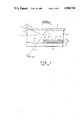
- FIG. 1 is a side cross sectional view with a part cut away showing the main section of the foregoing contact type image reading apparatus. An outline of this apparatus will be described.
- Reference numeral 8 denotes a photo sensor.
- the photo sensor 8 is arranged on a transparent substrate made of glass or the like in the direction perpendicular to the drawing and constitutes a one-dimensional line sensor.
- a light shielding layer 12 made of metal or the like and an insulative layer 13 are formed on the transparent substrate such as a glass.
- a semiconductor layer 14 made of amorphous silicon hydride (hereinafter abbreviated to A-Si:H), CdS.Se, or the like serving as a photoconductive layer is formed on the insulative layer 13.
- a pair of main electrodes 16 and 17 are formed through a doping semiconductor layer 15 for ohmic contact.
- a light receiving window 18 is formed between the main electrodes 16 and 17.
- a light L enters through an incident window 19 of the transparent substrate 11 (the photo sensor 8 is shielded against this incident light by the light shielding layer 12).
- An original P is illuminated by the incident light L.
- the reflected light is received by the photo sensor 8 and converted into an electric signal.
- This signal is taken out of the photo sensor 8 through electrode wiring (not shown) Namely, for example, assuming that a potential of the main electrode 16 is a reference potential and a drive voltage of a high potential is applied to the main electrode 17, when the reflected light L enters the surface of the semiconductor layer 14 through the light receiving window 18, the charges increase. Thus, the resistance decreases and this resistance change can be read as image information.
- the light from a light source 30 enters from the back side of the substrate 11.
- the direct light from the light source 30 enters the photo sensor 8 in addition to the reflected light from the original surface
- a photo current by the direct light flows as a stationary current.
- the S/N ratio fairly deteriorates. Therefore, to prevent the direct light from the light source 30 entering the photo sensor 8, the light shielding layer 12 must be provided on the light source side of the photo sensor 8.
- the light shielding layer 12 is ordinarily made of metal in order to assure a high light shielding property with a thin film.
- an interval between the original P and the photo sensor 8 is generally set to about 0.1 mm a reading resolution within a range from 4 lines/mm to 8 lines/mm is obtained.
- this interval must be accurately controlled. Such a control of the interval is accomplished by coating a transparent protective layer 20 onto the upper surface of the photo sensor 8.
- Another object of the invention is to provide an image reading apparatus which can prevent the stray lights from entering the sides of a sensor substrate or from the surface and sides of a protective layer, or the like and can further improve the S/N ratio and can reduce the deterioration of a photo sensor caused by the light, as compared with the conventional apparatus.
- Still another object of the invention is to provide an image reading apparatus comprising: a light shielding layer arranged on the surface of a substrate which can transmit light; an insulative layer arranged on the light shielding layer; a photo sensor arranged on the insulative layer; and protective layers arranged on the photo sensor, wherein the reflected light of the light irradiated onto the surface of an original from the back side of a substrate is received by the photo sensor, thereby reading image information, and light shielding means are provided to at least parts of the sides of the substrate and of the surface and sides of the protective layer.
- Still another object of the invention is to provide an image reading apparatus comprising a light shielding layer arranged on the surface of a substrate which can transmit light, a photo sensor formed directly on or formed indirectly over the light shielding layer, and protective layers arranged on the photo sensor, wherein light shielding means are provided on the sides of the substrate and protective layers.
- Still another object of the invention is to provide a reading apparatus comprising: an image reading apparatus having (a) a light shielding layer arranged on the surface of a substrate which can transmit light, (b) a photo sensor formed directly on or formed indirectly over the light shielding layer, (c) protective layers arranged on the photo sensor, and (d) light shielding means arranged on the sides of the substrate and/or the protective layers; moving means for relatively moving an original for the image reading apparatus in close vicinity to or in contact with the protective layers; and a light source to illuminate the original.
- FIG. 1 is a schematic side cross sectional view showing an example of a conventional image reading apparatus
- FIG. 2(A) is a schematic plan view of a line sensor according to one aspect of an embodiment of the invention.
- FIG. 2(B) is a schematic cross sectional view taken along the line B-B' in FIG. 2(A);
- FIG. 2(C) is a schematic cross sectional view taken along the line C-C' in FIG. 2(A);
- FIG. 3 is a schematic constitutional diagram of an image reading apparatus using the line sensor shown in FIGS. 2(A), 2(B),and 2(C).
- FIG. 2(A) is a schematic plan view of a line sensor according to one aspect of a preferred embodiment of the invention.
- FIGS. 2(B) and 2(C) are schematic cross sectional views taken along the lines B-B' and C-C' in FIG. 2(A).
- reference numeral 210 denotes a matrix wiring section; 208 indicates a photo sensor section; 212 is a charge accumulating section; 213 a switch section including a transfer switch 213a and a discharge switch 213b to reset charges in the charge accumulating section 213; 214 a wiring to connect a signal output of the transfer switch 213a with a signal processing section, which will be explained hereinafter; 223 a load capacitor to accumulate and read out the charges transferred by the transfer switch 213a; and 234 a light shielding member to shut out stray lights.
- an A-Si:H film is used as a photoconductive semiconductor layer 204 constituting the photo sensor section 208, transfer switch 213a; and discharge switch 213b.
- a silicon nitride (SiNH) film which is formed by glow discharge is used as an insulative layer 203.
- the photoconductive semiconductor layer 204, insulative layer 203, and protective layers 229, 230, and 232 are not shown.
- the photoconductive semiconductor layer 204 and insulative layer 203 are formed not only in the photo sensor section 208, charge accumulating section 212, transfer switch 213a, and discharge switch 213b, but also between the upper layer electrode wiring and the substrate.
- an A-Si:H layer 205 which is doped to n + is formed on the interface between the upper electrode wiring and the photoconductive semiconductor layer, thereby obtaining the ohmic contact.
- all of the signal paths which are output from respective sensor sections are arranged so as not to cross the other wirings, thereby preventing the generation of crosstalk among signal components and the induction noise from the gate electrode wiring.
- reference numerals 216 and 217 denote upper electrode wirings.
- the light enters from an incident window 219 and is reflected by the surface of an original. This reflected light changes a conductivity of the photoconductive semiconductor layer 204 in the photo sensor section 208, thereby changing a current flowing between upper layer electrode wirings 216 and 217 which face each other like a comb.
- Reference numeral 202 denotes a light shielding layer made of, e.g., metal. The light shielding layer 202 is connected to a proper drive section and prevents direct light from the light source from entering the photo sensor section 208.
- the charge accumulating section 212 comprises: the lower layer electrode wiring 214; a dielectric layer consisting of the insulative layer 203 and photoconductive semiconductor layer 204 which are formed on the lower layer electrode wiring 214; and a wiring which is formed on the photoconductive semiconductor layer 204 and continues with the upper layer electrode wiring 217 in the photo sensor section.
- the charge accumulating section 212 has the same structure as a so-called MIS (Metal Insulator Semiconductor) capacitor. Although either the positive or negative bias condition can be used, the stable capacitance and frequency characteristic can be obtained by always setting the lower layer electrode wiring 214 to a negative bias condition.
- FIG. 2(C) shows the switch section of a TFT structure including the transfer switch 213a and discharge switch 213b.
- the transfer switch 213a comprises: a lower layer electrode wiring 224 serving as a gate electrode; the insulative layer 203 serving as a gate insulative layer; the photoconductive semiconductor layer 204; an upper layer electrode wiring 225 serving as a source electrode; the upper layer electrode wiring 217 serving as a drain electrode; and the like.
- the gate insulative layer and photoconductive semiconductor layer of the discharge switch 213b are the same layers as the insulative layer 203 and photoconductive semiconductor layer 204.
- the source electrode corresponds to the upper layer electrode wiring 217.
- the gate electrode corresponds to a lower layer electrode wiring 227.
- the drain electrode corresponds to an upper layer electrode wiring 226.
- a lower layer wiring 233 is connected to a gate electrode of the transfer switch 213a.
- the protective layers 229, 230, and 232 having a 3-layer structure are formed on the photo sensor section 208. Since the first protective layer 230 directly comes into contact with the photo sensor section 208 or the like, an inorganic thin film such as SiO 2 film or SiNH film is used as a material of high purity which can stabilize the surface of the photo sensor section 208 or the like. Or, an organic film such as polyimide resin is used as such a material since a film can be easily formed. An epoxy resin or the like having an excellent adhesive property is used as a material of the second protective layer 229 in order to improve moisture resistance.
- an inorganic thin film such as SiO 2 film or SiNH film
- an organic film such as polyimide resin is used as such a material since a film can be easily formed.
- An epoxy resin or the like having an excellent adhesive property is used as a material of the second protective layer 229 in order to improve moisture resistance.
- the third protective layer 232 As a material having an abrasion resistance and a high light transmittivity, a thin plate glass such as borosilicate glass is used to form the third protective layer 232.
- the second protective layer 229 also functions as an adhesive agent.
- the protective layers have a laminated structure in which a plurality of functions which cannot be satisfied by the same material are provided for the respective layers. In other words, the functions are separated, thereby assuring the environmental resistance property of the line sensor.
- all of the composing sections of the photo sensor section, charge accumulating section, transfer switch, discharge switch, and matrix wiring section have a laminated structure consisting of the photoconductive semiconductor layer, insulative layer, protective layer, and the like. Therefore, those sections can be simultaneously formed by the same process.
- FIG. 3 is a schematic constitutional cross sectional view showing one aspect of a preferred embodiment of an image reading apparatus using the foregoing line sensor.
- reference numeral 208 denotes the photo sensor section which is arranged on the transparent substrate 201 in the direction perpendicular to the drawing and constructs a one-dimensional line sensor 235.
- the line sensor 235 is made of a conductive material such as metal and put on a holding member 236 having a slit 239. When image information of the original P is read, the line sensor 235 comes into contact with the original P which is conveyed by a feed roller R.
- a light source 237 is arranged so as to face the line sensor 235 through the holding member 236.
- An LED which has conventionally been used can be used as the light source 237.
- Reference numeral 238 denotes a lamp protective member made of a conductive material such as metal.
- the lamp protective member 238 is provided to mechanically protect light source 237 and to seal radiation noise which is generated from the light source 237.
- the light shielding member 234 prevents stray lights L' from entering the sides of the transparent substrate 201 and protective layers 229, 230, and 232 and from the surface of the protective layer 232.
- the light L emitted from the discharge tube light source 237 passes through the slit 239 of the holding member 236 and through the incident window 219 on the transparent substrate 201 and illuminates an image on the original P to be read.
- the reflected light is received by the photo sensor section 208.
- the stray lights other than the light to illuminate the original enter from the sides of the transparent substrate or from the sides and surface of an arbitrary protective layer and are reflected and scattered and illuminate not only the photo sensor section but also the capacitor section or switch section, the signal level is shifted or a malfunction is caused. Further, even in the cases other than the image reading time or even when the light source is lit off, if the stray lights always illuminate the photo sensor section or the like, the photo sensor section is deteriorated by the stray lights, so that the reliability of the photo sensor over a period of time will decay.
- the light shielding members 234 are provided on the sides of the transparent substrate 201 and protective layers 229, 230, and 232 and on the surface of the protective layer 232. Due to this structure, it is possible to realize an image reading apparatus in which the foregoing problems can be solved, a good S/N ratio is obtained deterioration caused by stray light is reduced, and the apparatus can be used for a long time.
- any material can be used if it can prevent transmission of stray light, and can be adhesively secured to the substrate 201, protective layers 229, 230, and 232, holding member 236, and the like.
- a substantially non-light transmitting organic resin or paint or the like is used in consideration of the easiness with which it forms the light shielding member and its low cost. It is desirable that the color of such resin or paint be a dark color such as black, deep blue, dark green, or the like.
- the invention is not limited to only the structure of the embodiment but can also use a structure such as to shut out the stray lights other than the light which illuminates the original by providing the light shielding means to at least parts of the sides of the photo sensor substrate or to parts of the sides and surface of the protective layers.
- the protective layers of a laminated structure in which a plurality of functions are provided for the respective layers at least one of the functions of the protective layers is added to the light shielding member and it is packaged so as to surround the substrate and protective layers. Due to this, a degree of freedom in selection of the material of the protective layer is increased and the stability of the image reading apparatus in the environment is further improved.
- an image reading apparatus comprising: a light shielding layer arranged on a substrate which can transmit light; an insulative layer formed on the light shielding layer; a photo sensor formed directly on or formed indirectly over the insulative layer; and protective layers arranged on and over the photo sensor, wherein the reflected light of the light irradiated onto the surface of an original from the back side of the substrate is received by the photo sensor, thereby reading image information.
- this apparatus by providing light shielding means on at least portions of the sides of the substrate or of the surface and sides of the protective layers, stray lights other than the light to which illuminates the original are prevented from entering the sides of the substrate and protective layers and enter the photo sensor section and, further, the switch section.
- the material having at least one of the functions of the protective layers is selected and formed on the sides of the substrate. Consequently, a degree of freedom in selection of the material constituting the protective layers increases and, at the same time, an image reading apparatus with improved environmental stability is obtained.
Abstract
Description
Claims (37)
Applications Claiming Priority (2)
| Application Number | Priority Date | Filing Date | Title |
|---|---|---|---|
| JP62-172008 | 1987-07-09 | ||
| JP62172008A JPS6415970A (en) | 1987-07-09 | 1987-07-09 | Image reading equipment |
Publications (1)
| Publication Number | Publication Date |
|---|---|
| US4908718A true US4908718A (en) | 1990-03-13 |
Family
ID=15933811
Family Applications (1)
| Application Number | Title | Priority Date | Filing Date |
|---|---|---|---|
| US07/213,848 Expired - Lifetime US4908718A (en) | 1987-07-09 | 1988-06-30 | Image reading apparatus having a light shielding layer arranged on the sides of the substrate and protective layers of a photo sensor |
Country Status (4)
| Country | Link |
|---|---|
| US (1) | US4908718A (en) |
| EP (1) | EP0298458B1 (en) |
| JP (1) | JPS6415970A (en) |
| DE (1) | DE3856106D1 (en) |
Cited By (26)
| Publication number | Priority date | Publication date | Assignee | Title |
|---|---|---|---|---|
| US4883459A (en) * | 1983-07-29 | 1989-11-28 | Reynaldo Calderon | Retrograde perfusion |
| US4970606A (en) * | 1988-07-27 | 1990-11-13 | Ricoh Company, Ltd. | Document reading apparatus |
| US4977313A (en) * | 1988-03-14 | 1990-12-11 | Hitachi, Ltd. | Facsimile equipment with direct-contact-type image sensor |
| US5015837A (en) * | 1988-11-02 | 1991-05-14 | Ricoh Company, Ltd. | Contact type image sensor with electric shielding |
| US5060040A (en) * | 1987-11-14 | 1991-10-22 | Canon Kabushiki Kaisha | Photoelectric conversion apparatus |
| US5101285A (en) * | 1989-07-24 | 1992-03-31 | Canon Kabushiki Kaisha | Photoelectric conversion device having an improved illuminating system and information processing apparatus mounting the device |
| US5121225A (en) * | 1989-02-21 | 1992-06-09 | Canon Kabushiki Kaisha | Photoelectric converter and image reading apparatus mounting the same |
| US5126859A (en) * | 1989-06-14 | 1992-06-30 | Sharp Kabushiki Kaisha | Contact type image sensor |
| US5134274A (en) * | 1991-03-18 | 1992-07-28 | Hughes Aircraft Company | Two-sided solid-state imaging device |
| US5162644A (en) * | 1988-03-14 | 1992-11-10 | Hitachi, Ltd. | Contact type image sensor having photoelectric conversion elements to reduce signal variation caused by luminous intensity variation of light source |
| US5196691A (en) * | 1989-11-21 | 1993-03-23 | Canon Kabushiki Kaisha | Photoelectric converting device having original conveyance guide and an image processing apparatus incorporating the device |
| US5233178A (en) * | 1991-03-29 | 1993-08-03 | Nec Corporation | Contact type image sensor and method of producing the same |
| US5261013A (en) * | 1989-02-21 | 1993-11-09 | Canon Kabushiki Kaisha | Photoelectric converter and image reading apparatus mounting the same |
| US5581076A (en) * | 1993-10-14 | 1996-12-03 | Canon Kabushiki Kaisha | Contact type image sensor with more-unified construction |
| US5604606A (en) * | 1990-07-06 | 1997-02-18 | Ricoh Company, Ltd. | Picture reading apparatus with flaring light elimination capability |
| US5635707A (en) * | 1994-05-30 | 1997-06-03 | Nec Corporation | Photoelectric conversion device for use in sensing light reflected from medium surface |
| US5703355A (en) * | 1993-04-20 | 1997-12-30 | Sony Corporation | Image sensor covered by a protective film and an organic film to decrease variations in spectral sensitivity |
| US5767559A (en) * | 1991-05-24 | 1998-06-16 | Fuji Xerox Co., Ltd. | Thin film type photoelectric conversion device |
| US5793047A (en) * | 1995-09-28 | 1998-08-11 | Canon Kabushiki Kaisha | Photoelectric conversion apparatus and X-ray image pickup apparatus |
| US5835142A (en) * | 1992-02-04 | 1998-11-10 | Matsushita Electric Industrial Co., Ltd. | Direct contact type image sensor and its production method |
| US5933550A (en) * | 1994-10-27 | 1999-08-03 | Nec Corporation | Data inputting device |
| US6075256A (en) * | 1993-12-16 | 2000-06-13 | Canon Kabushiki Kaisha | Photoelectric converter, its driving method, and system including the photoelectric converter |
| US20040227981A1 (en) * | 2003-02-24 | 2004-11-18 | Konica Minolta Business Technologies, Inc. | Image reading apparatus |
| US20100067065A1 (en) * | 2008-09-12 | 2010-03-18 | Canon Kabushiki Kaisha | Document reading apparatus |
| CN105489625A (en) * | 2015-11-26 | 2016-04-13 | 上海集成电路研发中心有限公司 | Lightproof storage capacitor structure employing global exposure picture element and forming method of lightproof storage capacitor structure |
| CN107518910A (en) * | 2016-06-20 | 2017-12-29 | 西门子医疗有限公司 | X-ray detector with opaque intermediate layer |
Families Citing this family (6)
| Publication number | Priority date | Publication date | Assignee | Title |
|---|---|---|---|---|
| KR0137398B1 (en) * | 1992-10-23 | 1998-04-29 | 모리시타 요이찌 | Fabrication method of sensor & unit |
| SE506654C2 (en) * | 1994-09-16 | 1998-01-26 | Sitek Electro Optics Ab | Position-sensitive photodetector with eliminated effect of jet light |
| JP4509022B2 (en) * | 2005-12-27 | 2010-07-21 | キヤノン株式会社 | Image reading apparatus and image forming apparatus |
| JP4533311B2 (en) * | 2005-12-27 | 2010-09-01 | キヤノン株式会社 | Image reading apparatus and image forming apparatus |
| US8149473B2 (en) | 2005-12-27 | 2012-04-03 | Canon Kabushiki Kaisha | Image reading apparatus |
| JP4533312B2 (en) * | 2005-12-27 | 2010-09-01 | キヤノン株式会社 | Image reading apparatus and image forming apparatus |
Citations (14)
| Publication number | Priority date | Publication date | Assignee | Title |
|---|---|---|---|---|
| US4189753A (en) * | 1978-06-08 | 1980-02-19 | Northern Telecom Limited | Document scanning head |
| US4305100A (en) * | 1979-07-09 | 1981-12-08 | Olympus Optical Company Limited | Light scanning device |
| JPS57190455A (en) * | 1981-05-19 | 1982-11-24 | Nippon Telegr & Teleph Corp <Ntt> | Adhesion type image sensor |
| US4395629A (en) * | 1979-12-10 | 1983-07-26 | Hitachi, Ltd. | Solid-state color imager and method of manufacturing the same |
| JPS5962267A (en) * | 1982-09-30 | 1984-04-09 | Kyocera Corp | Contact type reader |
| US4455577A (en) * | 1981-08-21 | 1984-06-19 | Canon Kabushiki Kaisha | Original reader |
| JPS6020675A (en) * | 1983-07-15 | 1985-02-01 | Ricoh Co Ltd | Picture inputting device |
| JPS6091759A (en) * | 1983-10-25 | 1985-05-23 | Kyocera Corp | Reader |
| US4689652A (en) * | 1984-03-12 | 1987-08-25 | Hitachi, Ltd. | Image sensor |
| US4768096A (en) * | 1984-05-04 | 1988-08-30 | Energy Conversion Devices, Inc. | Contact-type portable digitizing wand for scanning image-bearing surfaces |
| US4775895A (en) * | 1985-12-13 | 1988-10-04 | Heimann Gmbh | Modular image sensor structure |
| US4792859A (en) * | 1987-02-09 | 1988-12-20 | Ovonic Imaging Systems, Inc. | Digitizing wand adapted for manual and automatic operation |
| US4803375A (en) * | 1985-12-27 | 1989-02-07 | Kabushiki Kaisha Toshiba | Image sensors and methods of manufacturing same including semiconductor layer over entire substrate surface |
| US4839730A (en) * | 1986-05-20 | 1989-06-13 | Sharp Kabushiki Kaisha | Image reading apparatus |
Family Cites Families (12)
| Publication number | Priority date | Publication date | Assignee | Title |
|---|---|---|---|---|
| JPS5439590A (en) * | 1977-09-05 | 1979-03-27 | Nippon Telegr & Teleph Corp <Ntt> | Photo electric converter |
| JPS56138967A (en) * | 1980-03-31 | 1981-10-29 | Canon Inc | Photoelectric converter |
| JPS57173256A (en) * | 1981-04-20 | 1982-10-25 | Nippon Telegr & Teleph Corp <Ntt> | Image sensor |
| JPS57183177A (en) * | 1981-05-07 | 1982-11-11 | Canon Inc | Color solid-state image pickup device |
| JPS5840856A (en) * | 1981-09-03 | 1983-03-09 | Nippon Telegr & Teleph Corp <Ntt> | Array for photosensor |
| JPS6016758A (en) * | 1983-07-08 | 1985-01-28 | Canon Inc | Contact type image sensor |
| JPS6173472A (en) * | 1984-09-19 | 1986-04-15 | Canon Inc | Optical picture reader |
| JPH0658950B2 (en) * | 1985-02-18 | 1994-08-03 | 松下電器産業株式会社 | Contact image sensor |
| JPS61214563A (en) * | 1985-03-20 | 1986-09-24 | Mitsubishi Electric Corp | Contact-type image sensor substrate |
| JPH0795792B2 (en) * | 1985-08-09 | 1995-10-11 | 松下電器産業株式会社 | Contact image sensor |
| JPH0628309B2 (en) * | 1985-10-03 | 1994-04-13 | 松下電器産業株式会社 | Contact image sensor |
| JPS6298555A (en) * | 1985-10-24 | 1987-05-08 | Mitsubishi Electric Corp | Light emitting display device |
-
1987
- 1987-07-09 JP JP62172008A patent/JPS6415970A/en active Pending
-
1988
- 1988-06-30 US US07/213,848 patent/US4908718A/en not_active Expired - Lifetime
- 1988-07-06 DE DE3856106T patent/DE3856106D1/en not_active Expired - Lifetime
- 1988-07-06 EP EP88110798A patent/EP0298458B1/en not_active Expired - Lifetime
Patent Citations (14)
| Publication number | Priority date | Publication date | Assignee | Title |
|---|---|---|---|---|
| US4189753A (en) * | 1978-06-08 | 1980-02-19 | Northern Telecom Limited | Document scanning head |
| US4305100A (en) * | 1979-07-09 | 1981-12-08 | Olympus Optical Company Limited | Light scanning device |
| US4395629A (en) * | 1979-12-10 | 1983-07-26 | Hitachi, Ltd. | Solid-state color imager and method of manufacturing the same |
| JPS57190455A (en) * | 1981-05-19 | 1982-11-24 | Nippon Telegr & Teleph Corp <Ntt> | Adhesion type image sensor |
| US4455577A (en) * | 1981-08-21 | 1984-06-19 | Canon Kabushiki Kaisha | Original reader |
| JPS5962267A (en) * | 1982-09-30 | 1984-04-09 | Kyocera Corp | Contact type reader |
| JPS6020675A (en) * | 1983-07-15 | 1985-02-01 | Ricoh Co Ltd | Picture inputting device |
| JPS6091759A (en) * | 1983-10-25 | 1985-05-23 | Kyocera Corp | Reader |
| US4689652A (en) * | 1984-03-12 | 1987-08-25 | Hitachi, Ltd. | Image sensor |
| US4768096A (en) * | 1984-05-04 | 1988-08-30 | Energy Conversion Devices, Inc. | Contact-type portable digitizing wand for scanning image-bearing surfaces |
| US4775895A (en) * | 1985-12-13 | 1988-10-04 | Heimann Gmbh | Modular image sensor structure |
| US4803375A (en) * | 1985-12-27 | 1989-02-07 | Kabushiki Kaisha Toshiba | Image sensors and methods of manufacturing same including semiconductor layer over entire substrate surface |
| US4839730A (en) * | 1986-05-20 | 1989-06-13 | Sharp Kabushiki Kaisha | Image reading apparatus |
| US4792859A (en) * | 1987-02-09 | 1988-12-20 | Ovonic Imaging Systems, Inc. | Digitizing wand adapted for manual and automatic operation |
Cited By (39)
| Publication number | Priority date | Publication date | Assignee | Title |
|---|---|---|---|---|
| US4883459A (en) * | 1983-07-29 | 1989-11-28 | Reynaldo Calderon | Retrograde perfusion |
| US5060040A (en) * | 1987-11-14 | 1991-10-22 | Canon Kabushiki Kaisha | Photoelectric conversion apparatus |
| US5162644A (en) * | 1988-03-14 | 1992-11-10 | Hitachi, Ltd. | Contact type image sensor having photoelectric conversion elements to reduce signal variation caused by luminous intensity variation of light source |
| US4977313A (en) * | 1988-03-14 | 1990-12-11 | Hitachi, Ltd. | Facsimile equipment with direct-contact-type image sensor |
| US4970606A (en) * | 1988-07-27 | 1990-11-13 | Ricoh Company, Ltd. | Document reading apparatus |
| US5015837A (en) * | 1988-11-02 | 1991-05-14 | Ricoh Company, Ltd. | Contact type image sensor with electric shielding |
| US5261013A (en) * | 1989-02-21 | 1993-11-09 | Canon Kabushiki Kaisha | Photoelectric converter and image reading apparatus mounting the same |
| US5121225A (en) * | 1989-02-21 | 1992-06-09 | Canon Kabushiki Kaisha | Photoelectric converter and image reading apparatus mounting the same |
| US5126859A (en) * | 1989-06-14 | 1992-06-30 | Sharp Kabushiki Kaisha | Contact type image sensor |
| US5101285A (en) * | 1989-07-24 | 1992-03-31 | Canon Kabushiki Kaisha | Photoelectric conversion device having an improved illuminating system and information processing apparatus mounting the device |
| US5196691A (en) * | 1989-11-21 | 1993-03-23 | Canon Kabushiki Kaisha | Photoelectric converting device having original conveyance guide and an image processing apparatus incorporating the device |
| US5352883A (en) * | 1989-11-21 | 1994-10-04 | Canon Kabushiki Kaisha | Photoelectric converting device having original conveyance guide and an image processing apparatus incorporating the device |
| US5621206A (en) * | 1989-11-21 | 1997-04-15 | Canon Kabushiki Kaisha | Method of producing a photoelectric converting device |
| US5604606A (en) * | 1990-07-06 | 1997-02-18 | Ricoh Company, Ltd. | Picture reading apparatus with flaring light elimination capability |
| US5134274A (en) * | 1991-03-18 | 1992-07-28 | Hughes Aircraft Company | Two-sided solid-state imaging device |
| US5233178A (en) * | 1991-03-29 | 1993-08-03 | Nec Corporation | Contact type image sensor and method of producing the same |
| US5767559A (en) * | 1991-05-24 | 1998-06-16 | Fuji Xerox Co., Ltd. | Thin film type photoelectric conversion device |
| US5835142A (en) * | 1992-02-04 | 1998-11-10 | Matsushita Electric Industrial Co., Ltd. | Direct contact type image sensor and its production method |
| US5703355A (en) * | 1993-04-20 | 1997-12-30 | Sony Corporation | Image sensor covered by a protective film and an organic film to decrease variations in spectral sensitivity |
| US5581076A (en) * | 1993-10-14 | 1996-12-03 | Canon Kabushiki Kaisha | Contact type image sensor with more-unified construction |
| US6075256A (en) * | 1993-12-16 | 2000-06-13 | Canon Kabushiki Kaisha | Photoelectric converter, its driving method, and system including the photoelectric converter |
| US20060027758A1 (en) * | 1993-12-27 | 2006-02-09 | Canon Kabushiki Kaisha | Photoelectric converter, its driving method, and system including the photoelectric converter |
| USRE42157E1 (en) | 1993-12-27 | 2011-02-22 | Canon Kabushiki Kaisha | Photoelectric converter, its driving method, and system including the photoelectric converter |
| USRE39780E1 (en) * | 1993-12-27 | 2007-08-21 | Canon Kabushiki Kaisha | Photoelectric converter, its driving method, and system including the photoelectric converter |
| US6512279B2 (en) | 1993-12-27 | 2003-01-28 | Canon Kabushiki Kaisha | Photoelectric converter, its driving method, and system including the photoelectric converter |
| US20040159901A1 (en) * | 1993-12-27 | 2004-08-19 | Canon Kabushiki Kaisha | Photoelectric converter, its driving method, and system including the photoelectric converter |
| US7022997B2 (en) | 1993-12-27 | 2006-04-04 | Canon Kabushiki Kaisha | Photoelectric converter, its driving method, and system including the photoelectric converter |
| US6982422B2 (en) | 1993-12-27 | 2006-01-03 | Canon Kabushiki Kaisha | Photoelectric converter, its driving method, and system including the photoelectric converter |
| US5635707A (en) * | 1994-05-30 | 1997-06-03 | Nec Corporation | Photoelectric conversion device for use in sensing light reflected from medium surface |
| US6377715B1 (en) | 1994-10-27 | 2002-04-23 | Nec Corporation | Data inputting device |
| US5933550A (en) * | 1994-10-27 | 1999-08-03 | Nec Corporation | Data inputting device |
| US5793047A (en) * | 1995-09-28 | 1998-08-11 | Canon Kabushiki Kaisha | Photoelectric conversion apparatus and X-ray image pickup apparatus |
| US20040227981A1 (en) * | 2003-02-24 | 2004-11-18 | Konica Minolta Business Technologies, Inc. | Image reading apparatus |
| US20100067065A1 (en) * | 2008-09-12 | 2010-03-18 | Canon Kabushiki Kaisha | Document reading apparatus |
| US8270042B2 (en) * | 2008-09-12 | 2012-09-18 | Canon Kabushiki Kaisha | Document reading apparatus |
| CN105489625A (en) * | 2015-11-26 | 2016-04-13 | 上海集成电路研发中心有限公司 | Lightproof storage capacitor structure employing global exposure picture element and forming method of lightproof storage capacitor structure |
| CN105489625B (en) * | 2015-11-26 | 2018-08-28 | 上海集成电路研发中心有限公司 | A kind of light leakage storage capacitor construction and forming method thereof of global exposure pixel |
| CN107518910A (en) * | 2016-06-20 | 2017-12-29 | 西门子医疗有限公司 | X-ray detector with opaque intermediate layer |
| CN107518910B (en) * | 2016-06-20 | 2021-09-03 | 西门子医疗有限公司 | X-ray detector with opaque intermediate layer |
Also Published As
| Publication number | Publication date |
|---|---|
| EP0298458A3 (en) | 1991-02-27 |
| EP0298458B1 (en) | 1998-01-14 |
| JPS6415970A (en) | 1989-01-19 |
| DE3856106D1 (en) | 1998-02-19 |
| EP0298458A2 (en) | 1989-01-11 |
Similar Documents
| Publication | Publication Date | Title |
|---|---|---|
| US4908718A (en) | Image reading apparatus having a light shielding layer arranged on the sides of the substrate and protective layers of a photo sensor | |
| US5086218A (en) | Photo sensor and its manufacturing method and an image reading apparatus having this photo sensor | |
| US5017988A (en) | Image reading device with protective layers | |
| US4922117A (en) | Photoelectric conversion device having a constant potential wiring at the sides of the common wiring | |
| JP3008859B2 (en) | Image sensor device using thin light source | |
| WO2004008538A1 (en) | Photoelectric conversion device, image scanning apparatus, and manufacturing method of the photoelectric conversion device | |
| US6002139A (en) | Image input device having a refractive index light guide and lenses | |
| US4541015A (en) | Two-dimensional image readout device | |
| JP2928043B2 (en) | Complete contact image sensor | |
| US4845375A (en) | Contact photoelectric conversion apparatus having plurality of protecting layers | |
| US5144458A (en) | Total contact type image sensor | |
| JP2830177B2 (en) | Image reading device | |
| JP2815134B2 (en) | Image reading apparatus and image information reading apparatus having the same | |
| JPH01179356A (en) | Hybrid integrated photoelectric converter array | |
| JPS6317554A (en) | Photoconductive device | |
| JP2769812B2 (en) | Document reading device | |
| US5204762A (en) | Image reading device | |
| JP2959854B2 (en) | Image reading device | |
| JPH029499B2 (en) | ||
| JPS6124271A (en) | Image sensor | |
| JPH07107930B2 (en) | Photoelectric conversion device manufacturing method | |
| JPH04291762A (en) | Communication terminal using image reader | |
| JPH01119061A (en) | Photoelectric conversion device | |
| JPH0728017B2 (en) | Image reader | |
| JPS60210867A (en) | Linear image sensor |
Legal Events
| Date | Code | Title | Description |
|---|---|---|---|
| AS | Assignment |
Owner name: CANON KABUSHIKI KAISHA, 30-2, 3-CHOME, SHIMOMARUKO Free format text: ASSIGNMENT OF ASSIGNORS INTEREST.;ASSIGNOR:SHIMADA, TETSUYA;REEL/FRAME:004894/0803 Effective date: 19880627 |
|
| STCF | Information on status: patent grant |
Free format text: PATENTED CASE |
|
| CC | Certificate of correction | ||
| FPAY | Fee payment |
Year of fee payment: 4 |
|
| FPAY | Fee payment |
Year of fee payment: 8 |
|
| FEPP | Fee payment procedure |
Free format text: PAYER NUMBER DE-ASSIGNED (ORIGINAL EVENT CODE: RMPN); ENTITY STATUS OF PATENT OWNER: LARGE ENTITY Free format text: PAYOR NUMBER ASSIGNED (ORIGINAL EVENT CODE: ASPN); ENTITY STATUS OF PATENT OWNER: LARGE ENTITY |
|
| FPAY | Fee payment |
Year of fee payment: 12 |