US4901330A - Optically pumped laser - Google Patents
Optically pumped laser Download PDFInfo
- Publication number
- US4901330A US4901330A US07/221,670 US22167088A US4901330A US 4901330 A US4901330 A US 4901330A US 22167088 A US22167088 A US 22167088A US 4901330 A US4901330 A US 4901330A
- Authority
- US
- United States
- Prior art keywords
- laser
- strip
- optically pumped
- accordance
- active
- Prior art date
- Legal status (The legal status is an assumption and is not a legal conclusion. Google has not performed a legal analysis and makes no representation as to the accuracy of the status listed.)
- Expired - Fee Related
Links
Images
Classifications
-
- H—ELECTRICITY
- H01—ELECTRIC ELEMENTS
- H01S—DEVICES USING THE PROCESS OF LIGHT AMPLIFICATION BY STIMULATED EMISSION OF RADIATION [LASER] TO AMPLIFY OR GENERATE LIGHT; DEVICES USING STIMULATED EMISSION OF ELECTROMAGNETIC RADIATION IN WAVE RANGES OTHER THAN OPTICAL
- H01S3/00—Lasers, i.e. devices using stimulated emission of electromagnetic radiation in the infrared, visible or ultraviolet wave range
- H01S3/09—Processes or apparatus for excitation, e.g. pumping
- H01S3/091—Processes or apparatus for excitation, e.g. pumping using optical pumping
- H01S3/094—Processes or apparatus for excitation, e.g. pumping using optical pumping by coherent light
- H01S3/0941—Processes or apparatus for excitation, e.g. pumping using optical pumping by coherent light of a laser diode
- H01S3/09415—Processes or apparatus for excitation, e.g. pumping using optical pumping by coherent light of a laser diode the pumping beam being parallel to the lasing mode of the pumped medium, e.g. end-pumping
-
- H—ELECTRICITY
- H01—ELECTRIC ELEMENTS
- H01S—DEVICES USING THE PROCESS OF LIGHT AMPLIFICATION BY STIMULATED EMISSION OF RADIATION [LASER] TO AMPLIFY OR GENERATE LIGHT; DEVICES USING STIMULATED EMISSION OF ELECTROMAGNETIC RADIATION IN WAVE RANGES OTHER THAN OPTICAL
- H01S5/00—Semiconductor lasers
- H01S5/40—Arrangement of two or more semiconductor lasers, not provided for in groups H01S5/02 - H01S5/30
- H01S5/4025—Array arrangements, e.g. constituted by discrete laser diodes or laser bar
- H01S5/4031—Edge-emitting structures
- H01S5/4043—Edge-emitting structures with vertically stacked active layers
- H01S5/405—Two-dimensional arrays
-
- H—ELECTRICITY
- H01—ELECTRIC ELEMENTS
- H01S—DEVICES USING THE PROCESS OF LIGHT AMPLIFICATION BY STIMULATED EMISSION OF RADIATION [LASER] TO AMPLIFY OR GENERATE LIGHT; DEVICES USING STIMULATED EMISSION OF ELECTROMAGNETIC RADIATION IN WAVE RANGES OTHER THAN OPTICAL
- H01S3/00—Lasers, i.e. devices using stimulated emission of electromagnetic radiation in the infrared, visible or ultraviolet wave range
- H01S3/09—Processes or apparatus for excitation, e.g. pumping
- H01S3/091—Processes or apparatus for excitation, e.g. pumping using optical pumping
- H01S3/094—Processes or apparatus for excitation, e.g. pumping using optical pumping by coherent light
- H01S3/09408—Pump redundancy
-
- H—ELECTRICITY
- H01—ELECTRIC ELEMENTS
- H01S—DEVICES USING THE PROCESS OF LIGHT AMPLIFICATION BY STIMULATED EMISSION OF RADIATION [LASER] TO AMPLIFY OR GENERATE LIGHT; DEVICES USING STIMULATED EMISSION OF ELECTROMAGNETIC RADIATION IN WAVE RANGES OTHER THAN OPTICAL
- H01S3/00—Lasers, i.e. devices using stimulated emission of electromagnetic radiation in the infrared, visible or ultraviolet wave range
- H01S3/09—Processes or apparatus for excitation, e.g. pumping
- H01S3/091—Processes or apparatus for excitation, e.g. pumping using optical pumping
- H01S3/094—Processes or apparatus for excitation, e.g. pumping using optical pumping by coherent light
- H01S3/094096—Multi-wavelength pumping
-
- H—ELECTRICITY
- H01—ELECTRIC ELEMENTS
- H01S—DEVICES USING THE PROCESS OF LIGHT AMPLIFICATION BY STIMULATED EMISSION OF RADIATION [LASER] TO AMPLIFY OR GENERATE LIGHT; DEVICES USING STIMULATED EMISSION OF ELECTROMAGNETIC RADIATION IN WAVE RANGES OTHER THAN OPTICAL
- H01S5/00—Semiconductor lasers
- H01S5/40—Arrangement of two or more semiconductor lasers, not provided for in groups H01S5/02 - H01S5/30
- H01S5/4025—Array arrangements, e.g. constituted by discrete laser diodes or laser bar
- H01S5/4031—Edge-emitting structures
- H01S5/4043—Edge-emitting structures with vertically stacked active layers
-
- H—ELECTRICITY
- H01—ELECTRIC ELEMENTS
- H01S—DEVICES USING THE PROCESS OF LIGHT AMPLIFICATION BY STIMULATED EMISSION OF RADIATION [LASER] TO AMPLIFY OR GENERATE LIGHT; DEVICES USING STIMULATED EMISSION OF ELECTROMAGNETIC RADIATION IN WAVE RANGES OTHER THAN OPTICAL
- H01S5/00—Semiconductor lasers
- H01S5/40—Arrangement of two or more semiconductor lasers, not provided for in groups H01S5/02 - H01S5/30
- H01S5/4025—Array arrangements, e.g. constituted by discrete laser diodes or laser bar
- H01S5/4087—Array arrangements, e.g. constituted by discrete laser diodes or laser bar emitting more than one wavelength
Definitions
- the optically pumped laser includes a laser diode array for generating optically pumped radiation having a uniform intensity distributed over a broad bandwidth and a lasant material with an absorption band for absorbing radiation within the above bandwidth.
- a laser is a device which has the ability to produce monochromatic, coherent light through the stimulated emission of photons from atoms or molecules of an active medium or lasant material which have typically been excited from ground state to a higher energy level by an input of energy.
- Such a device contains an optical cavity or resonator which is defined by highly reflective surfaces which form a closed round trip path for light, and the active medium is contained within the optical cavity.
- the spontaneous emission of a photon from an excited atom or molecule returning to its ground state can stimulate the emission of photons of identical energy from other excited atoms or molecules.
- the initial photon creates a cascade of photons between the mirrors of the optical cavity which are of identical energy and exactly in phase. A portion of this cascade of photons is then discharged out of the optical cavity, for example, by transmission through one or more of the reflecting surfaces of the cavity.
- Excitation of the lasant material of a laser can be accomplished by a variety of methods, such as, by optical pumping, current injection or the use of an electrical discharge.
- Optical pumping involves the creation of a population inversion through the absorption of light by a lasant material.
- the use of light from noble gas arc lamps, tungsten-halogen lamps, light-emitting diodes, laser diodes and laser diode arrays to optically pump or excite the lasant material of a laser is well known.
- the photons delivered to the lasant material from a radiant source must be of a very precise character as within the absorption band of the lasant material.
- the pumping radiation must be of a wavelength which is absorbed by the lasant material to produce the required population inversion.
- U.S. Pat. No. 3,624,545 issued to Ross describes an optically pumped solid state laser composed of a neodymium-doped yttrium aluminum garnet (Nd:YAG) rod which is side-pumped by at least one semiconductor laser diode.
- Nd:YAG neodymium-doped yttrium aluminum garnet
- U.S. Pat. No. 3,753,145 issued to Chesler discloses the use of one or more light-emitting semiconductor diodes to end pump a Nd:YAG rod.
- the use of an array of pulsed laser diodes to end pump a solid lasant material such as neodymium-doped YAG is described in U.S. Pat. No. 3,982,201 issued to Rosenkrantz et al.
- Lasers such as semiconductor diode lasers, are activated by the application of an electrical current.
- Laser diodes are efficient pumps for optically pumped lasers since the output radiation from the laser pump is a single wavelength (or a very narrow band of wavelengths) which is selected in such a manner that matches the absorption band or peak of the lasant material to be optically pumped.
- the output radiation of the laser pump is generally of a single wavelength which is selected in such a manner so as to precisely match the absorption band peak of the lasant material which is to be optically pumped.
- the CW operating characteristics of the 15 best of 17 individually fabricated subarrays are given in Table 1 (of the Allen report), which includes the peak emission wavelength at 25° C. for 250 mA drive current.
- the distribution of the subarray is found in FIG. 4 (of the Allen report), which is a graph of the output power versus the peak emission wavelength. Twelve of the subarrays have peak emission wavelengths in the range of 805 nm plus or minus 5 nm. The other three have shorter wavelengths.
- the CW operating characteristics of the 2 worst of the 17 individually fabricated subarrays were ignored.
- U.S. Pat. No. 3,946,331 issued to Pollack et al. describes a Nernst lamp for optical pumping of a solid state laser.
- the lamp materials were selected so that the light emitted was essentially concentrated in the relatively narrow pump region of the absorption spectrum of the laser crystal.
- W. T. Tsang Appl. Phys. Letter, Vol. 36, No. 6, 1980, pp. 441-443 discloses a multiwavelength transverse-junction-stripe laser, which is capable of emitting multiple predominantly single-longitudinal mode emissions at various wavelengths.
- four different outputs at 902.5, 879.3, 853.2 and 827.6 nm were obtained simultaneously from a single-wavelength TJS laser.
- an optically pumped laser comprising a laser diode array for generating optical pumping radiation, such pumping radiation having a bandwidth which is about 3 nm to about 15 nm wide and wherein the intensity of the pumping radiation is substantially uniformly distributed over such bandwidth, and a lasant material with an absorption band for receiving radiation within the bandwidth of the laser diode array.
- the instant invention discloses an optically pumped laser which includes a laser diode array for generating optical pumping radiation having a uniform intensity distributed over a broad bandwidth, and a lasant material with an absorption band for receiving radiation within such bandwidth.
- An embodiment of the invention includes an optically pumped laser comprising: (a) a laser diode array for generating optical pumping radiation, said pumping radiation having a bandwidth which is about 3 nm to about 15 nm wide and wherein the intensity of the pumping radiation is substantially uniformly distributed over said bandwith, and (b) a lasant material with an absorption band for receiving radiation within said bandwidth of said laser diode array.
- An object of the invention is to provide an optically pumped laser which includes a laser diode array that emits optical pumping radiation having a uniform intensity over a broad bandwidth for providing stable pumping radiation to a lasant material, thereby providing an improved and more stable optically pumped laser which provides enhanced stability despite aging and temperature, pressure, and current variations.
- Another object of the invention is to provide an optically pumped laser that eases and relaxes the requirements of wavelength matching by providing a broad bandwidth output radiation from the laser to the absorption band of the lasant material.
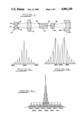
- FIG. 1 of the drawings is a schematic view representative of an embodiment of this invention.
- FIG. 2a is a graph of the emission spectrum of a conventional diode laser.
- FIG. 2b is a graph of the emission spectrum of a first diode array comprised of two strips suitable for use in the practice of this invention.
- FIG. 2c is a graph of the emission spectrum of a second diode array comprised of eleven strips suitable for use in the practice of this invention. A conventional laser diode array emission spectrum is also shown in phantom.
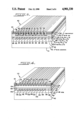
- FIG. 3 of the drawings is a perspective view of a laser diode array suitable for use in the practice of this invention.
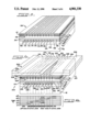
- FIG. 4 of the drawings is a perspective view of another laser diode array suitable for use in the practice of this invention.
- FIG. 5 of the drawings is a perspective view of yet another laser diode array suitable for use in the practice of this invention.
- FIG. 6a of the drawings is a perspective view partially cut away of yet another laser diode array suitable for use in the practice of this invention.
- FIG. 6b of the drawings is a graph of the temperature versus position of the laser diode array, as set forth in FIG. 6a.
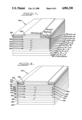
- FIG. 7 of the drawings is a perspective view of still another laser diode array suitable for use in the practice of this invention.
- FIG. 8 of the drawings is a perspective view of still another laser diode array suitable for use in the practice of this invention.
- FIG. 9 of the drawings is a perspective view of yet another laser diode array suitable for use in the practice of this invention.
- FIG. 10 of the drawings is a perspective view of another laser diode array suitable for use in the practice of this invention.
- FIG. 11 of the drawings is a perspective view of another laser diode array suitable for use in the practice of this invention.
- FIGS. 1-11 While this invention is susceptible of embodiments in many forms, there areshown in FIGS. 1-11 several specific embodiments suitable for use in the practice of this invention, with the understanding that the present disclosure is not intended to limit the invention to the embodiments illustrated.
- Laser diode array 10 consists of elements or heat sinks 12 and 14 with laser diodes or strips 13 and 15, respectively, attached thereto. Light from laser diodes 13 and 15, is guided by lens 16 into lasant material 18.
- a highly suitable optical laser diode array 10 consists of gallium aluminum arsenide laser diodes.
- the diode output radiation of 13 and 15 should substantially match the absorption band of lasant material 18. If lasant materials other than Nd:YAG are used, then appropriate semiconductor materials must be chosen to meet the above wavelength criteria.
- diode 13 emits light at a wavelength ofabout 2 nm or less below the absorption peak of the lasant material 18 and laser diode 15 emits light at a wavelength of about 2 nm or less above theabsorption peak at the lasant material 18.
- Laser diodes 13 and 15 can be tuned for the appropriate output radiation wavelength, by thermoelectric heaters/coolers, varying the aluminum and/or doping concentration in laserdiodes 13 and 15. Referring to FIG.
- laser diode 13 emits light at a wavelength ranging from about 806 nm to about 808 nm, preferably about 807.6 nm
- laser diode 15 emits light at a wavelength ranging from about 808 nm to about 810 nm, preferably about 808.4 nm, under lasing conditions.
- the absorption peak of the lasant material can vary from sample to sample. Accordingly, the above wavelength values are merely exemplary.
- the optical pumping means or laser diode array 10 with laser diodes 13 and 15, generates an optical pumping radiation having a bandwidth which is about 3 nm wide and wherein the intensity of the pumping radiation is substantially uniformly distributed over such bandwidth (see phantom (dashed) waveform in FIG. 2b).
- the waveform in FIG.2b represents a situation where the longitudinal waveforms exactly overlap.Even if such waveform does not exactly overlap, a uniform intensity distributed over a broad bandwidth is obtained.
- the lasant material 18 with a fixed absorption band receives radiation within the above bandwidthfrom the laser diode array 10, as is shown in FIG. 1.
- Heat sinks 12 and 14 can be passive in character. Heat sinks 12 and 14 can also include a thermoelectric cooler to help maintain laser diodes 13 and 15 at a constant temperature and thereby ensure optimal operation of laserdiodes 13 and 15. During operation the laser diode array 10 will be attached to a suitable power supply. Electrical leads from laser diodes 13and 15 which are connected to a power supply are not illustrated in FIG. 1.
- Lasant material 18 has a suitable reflective coating on input surface 20 and is capable of being pumped by the light from laser diode array 10.
- Thelasant material 18 also has an output surface 22.
- the reflective coating oninput surface 20 is highly transparent with respect to light produced by the laser diode array 10 but is highly reflective with respect to light produced by the lasing of lasant material 18.
- Nonlinear optical material 24 Light emitted by the lasing of lasant material 18 is passed through a nonlinear optical material 24 to output coupler 26 which has a suitable reflective coating on surface 28 which is highly reflective with respect to light emitted by lasant material 18 but substantially transparent to frequency-modified light produced by nonlinear optical material 24.
- Nonlinear optical material 24 has an output surface 25.
- Output coupler 26 is configured in such a manner so that it serves to collimate the output radiation from the laser which passes through it. It should be understood,however, that nonlinear optical material for 24 is not required for the practice of this invention, and merely represents a preferred embodiment of this invention.
- Laser diode array 10 has an emission spectrum or bandwith which is wider than or envelopes the absorption band of lasant material 18 which is beingpumped.
- the matching of laser light output from laser diode array 10 to lasant material 18 is less sensitive to temperature and current variations, and aging of laser diodes 13 and 15, than typical diode pumpedlasers because of the wide bandwidth of diode laser array 10 as illustratedin FIG. 2b.In FIG. 1, only two laser diodes 13 and 15 are shown. However, more than two laser diodes may be utilized.
- the bandwidth of laser diode array 10 in FIG. 2b is at least about twice as wide as a conventional laser diode, as illustrated in FIG. 2a.
- the laser diode array 10 does not require as sophisticated and sensitive feedback and thermoelectricheater/cooler circuitry to match the absorption band of the lasant material18, because the bandwidth of laser diode array 10 is wider than conventional narrow bandwidth laser diodes. Further, laser diode array 10 eases and relaxes the wavelength matching of array 10 to lasant material 18 by providing a broad bandwidth output radiation from array 10 to the absorption band of the lasant material 18, resulting in enhanced stabilitydespite aging and temperature, pressure and current variations.
- a stable and steady optically pumped laser such as the instant invention has a multitude of uses and is highly suitable for situations where environmental variations exist, such as but not limited to, metrology, laser printers, bar code readers, optical storage, medical applications, laser radars, etc. It is particularly advantageous in situations where severe environmental variations exist, such as but not limited to aerospace, automotive applications, industrial sensing, communications, gun sights, target designators and many military applications, etc.
- the laser diode array 10 overcomes the problems associated with narrow bandwidth laser diodes or arrays by sacrificing some power output to attain a steady and stable power output.
- Lens 16 serves to focus light from laser diodes 13 and 15 onto lasant material 18. This focusing results in a high pumping intensity and an associated high photon to photon conversion efficiency in lasant material 18. Any conventional optical means for focusing light can be used in placeof lens 16. For example, a gradient index lens, a ball lens, an aspheric lens or a combination of lenses can be utilized. Lens 16 is not essential to the operation of this invention, and the use of such focusing means merely represents a preferred embodiment.
- Suitable lasant materials include, for example, materials consisting of neodymium-doped yttrium vanadate (Nd:YV0 4 ); neodymium and/or cromium-doped gadolinium scandium galliumgarnet (Nd, Cr:GSGG); thallium, holmium and/or erbium-doped yttrium aluminum garnet (Tm, Ho, Er:YAG); titanium sapphire (Ti:A1 2 0 3 );glassy and crystalline host materials which are doped with an active material.
- a neodymium-doped YAG is a highly suitable lasant material 18 for use in combination with laser diode array 10 producing light having a wavelength of about 808 nm. When pumped with light of this wavelength, the neodymium-doped YAG or lasant material 18 can emit light having a wavelength of 1,064 nm.
- lasant material 18 can vary widely.
- thelasant material can have lens-shaped surfaces or be rhombohedral in shape if desired.
- an embodiment can include the use of a fiber of lasant material which is end-pumped by the optical pumping means 10.
- Highly suitable fibers for this purpose include,for example, glass optical fibers which are doped with ions of a rare earthmetal such as neodymium. If a very long fiber is required, it can be coiled, on a spool for example, in order to minimize the overall length ofthe laser of the instant invention.
- Lasant material 18 has a reflective coating on surface 20.
- This coating is conventional in character and is selected so as to transmit as much incident pumping radiation from laser diodes 13 and 15 as possible, while being highly reflective with respect to the radiation or light produced bythe lasing of lasant material 18.
- the coating on input surface 20 should be substantially transparent to 808 nm light and highly reflective with respect to light having a wavelength of 1,064 nm. In a preferred embodiment, this coating will also be highly reflective of light having a wavelength of 532 nm, the second harmonic of the aforementioned 1,064 nm light.
- the wavelength selective mirror which is created by the coating on input surface 20 need not be located on the input surface 20 of lasant material 18. If desired, this mirror can be located anywhere between laserdiode array 10 and the lasant material 18, and can consist of a coating deposited on any suitable substrate. In addition, the mirror can be of anysuitable shape.
- Nonlinear optical material 24 Light emitted by the lasing of lasant material 18 is passed through nonlinear optical material 24.
- the frequency of the incident light can be modified, for example, doubled or tripled, by passage through nonlinear optical material 24.
- light having awavelength of 1,064 nm from a neodymium-doped YAG lasant material 18 can beconverted to light having a wavelength of 532 nm upon passage through nonlinear optical material 24.
- the geometric shape of nonlinear optical material 24 can vary widely.
- the nonlinear optical material can have lens-shaped surfaces or be rhombohedral in shape if desired.
- any such nonlinear optical component can comprise heating or cooling means to control the temperature of the nonlinear optical material24 and thereby optimize its performance as a harmonic generator.
- Nonlinear optical material has an output surface 25.
- Potassium titanyl phosphate is a preferred nonlinear optical material 24.
- any of the many known nonlinear optical materials can be utilizedin the practice of this invention.
- Such known nonlinear optical materials can be a solid or a liquid, and can include, for example KH 2 PO 4 , LiNbO 3 , KNbO 3 , LiIO 3 , HIO 3 , KB 5 O 8 .sup.. 4H 2 O, urea and compounds of the formula MTiO(X04) where M is selected from the group consisting of K, Rb and Tl, and X s selected from the group consisting of P and As.
- the non-linear optical material 24 is not an essential component and its use represents one embodiment of this invention.
- nonlinear optical material 24 is not 100 percent efficient as a second harmonic generator
- light passing through this component from lasant material 18 will ordinarily consist of a mixture of frequency doubled or summed light and unmodified light.
- the light passed through nonlinear optical material 24 will be a mixture of 1,064 nm and 532 nm wavelengths. This mixture of wavelengths is directed to output coupler 26 which has a reflective coating on surface 28 which is wavelength selective.
- This coating is conventional in character and is selected in such a manner thatit is substantially transparent to the 532 nm light but highly reflective with respect to the 1,064 nm light. Accordingly, essentially only frequency doubled light having a wavelength of 532 nm is emitted through the output coupler 26.
- the output coupler 26 includes a wavelength selective mirror which is created by the coating on surface 28. It need not be of the precise designillustrated in FIG. 1, and can be of any conventional form.
- the wavelength selective mirror can be created by a coating on surface 25 of nonlinear optical material 24.
- output coupler 26 could be either eliminated or replaced by optical means whose sole purpose is tocollimate or otherwise modify the output radiation or laser light from the lasant material 20.
- the concave shape of the mirror created by the coating on surface 28 has the advantage of focusing reflected light, which has not been frequency doubled, back onto nonlinear optical material24, through lasant material 18 and onto the coating on input surface 20.
- this coating on surface 20 is highly reflective of both frequency doubled and unmodified light from the lasing of lasant material 18.
- frequency-unmodified light reflected by the coating on surface 28 is partially frequency doubled by passage through nonlinear optical material 24, the resulting mixture of wavelengths is reflected from the coating on input surface 20 back throughnonlinear optical material 24 where some of the residual frequency-unmodified light is frequency doubled, and the frequency doubledlight is emitted through output coupler 26.
- losses which may occur as a result of processes such as scattering or absorption further repetition of this series of events results in essentially all of the light produced by the lasing of lasant material 18 being frequency doubledand emitted through output coupler 26.
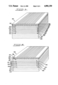
- FIG. 3 there is schematically shown a laser diode array 40 which is suitable for use as a source of optical pumping radiation in the practice of this invention.
- the fabrication of this diode array 40, as well as other laser structures hereinafter described, can be carried out by liquid-phase epitaxy, molecular beam epitaxy and metal-organic chemicalvapor deposition, which techniques are known in the art.
- Deposited on substrate 42 are layers 44, 46, 48, 50, 52, 54, and 56.
- Substrate 42 can be an n+GaAs substrate.
- Layers 44 and 52 are confining layers, typically about 1 ⁇ m thick, which can comprise nA1 x , Ga 1-x , As and pA1 x Ga 1-x As, respectively.
- Layers 46 and 50 are waveguide layers typically less than or about equal to 0.2 nm thick, which can comprise nA1 y , Ga 1-y , As and pA1 y Ga 1-y As, respectively.
- Layer 48 is an active region or quantum well having a thickness 49 typically less than or about equal to 0.2 ⁇ m, which can comprise iA1 z Ga 1-z As. Values for x and x', y and y', and z typically range from about 0.3 to 1.0, 0.1 to 0.5, and 0.0 to 0.1, respectively, but are not limited to such ranges.
- Layer 54 is a cap, typically less than or about equal to 0.2 ⁇ m thick, which can comprise p+GaAs.
- layer 56 is a conductive layer typically made of a gold/chromium composition or equivalent thereof.
- a power supply is not included in the figures.
- the laser diodes, light emitting lasers and laser diode arrays illustrated herein are properly forward biased by applying a positive charge at the appropriate place to energize laser diode array 40,and the other diode arrays in FIGS. 4-11.
- Layer 56 provides a metalization layer for electrode connection and current pumping.
- the bottom surface 41 of substrate 42 can be metalized to provide a contact for the other electrode connection. This metalization is conductive and can be made of a gold/tin or gold/germanium alloy.
- laser diode array In a conventional laser diode array, the number of strips is significant from the point of desired power output. Generally, an increase in the number of strips will proportionally increase the optical power output at a desired wavelength. See FIG. 2c in phantom wherein the emission spectrumof a conventional laser diode array centered at 808 nm is illustrated. Also, the higher the number of emitting cavities, the higher the obtainable peak power output.
- laser diode arrays include activelayers which have the highest index of refraction and a low bandwidth to provide a waveguide for light wave propagation at a single wavelength under lasing conditions.
- laser diode arrays require sensitive and sophisticated feedback circuitry and/or thermoelectric heaters/coolers to carefully match the output radiation of the array with the absorption peak of the lasant material, which is in sharp contrast to laser diode array 40.
- the bandwidth of the laser diode array 40 is wider than in conventional narrow bandwidth laser diodes, the radiation emitted therefrom is more stable and, less temperature and current sensitive, and less sensitive to aging variations.
- the current confining channel geometry shown in FIG. 3 comprises 11 parallel contact strips which run the length of diode array 40. However, any number of strips can be utilized in the practice of this invention.
- a conventional proton implant 57 is included which patterns lateral regions of high and low resistive material in a semi-conductor device to channel current to a specific region in a device when properly biased.
- Each of the above strips has varying widths for confining current flow to the plurality of strip areas or emitting cavities of the active layer 48.
- Each strip area emits pumping radiation under lasing conditions different from that of each adjacent strip area, thereby providing a stable, uniformly distributed wide bandwidth laser diode array which is less sensitive to temperature and current variations, and less sensitive to aging variations.
- the first strip 58 includes a width designated as a in FIG. 3, ranging from0.9 um to 1.1 um, preferably 1 um
- the second strip 60 includes a width b ranging from 1.12 um to 1.37 um, preferably 1.25 um
- the third strip 62 includes a width c ranging from 1.22 um to 1.73 um, preferably 1.57 um
- the fourth strip 64 includes a width d ranging from 1.8 um to 2.2 um, preferably 2 um
- the fifth strip 66 includes a width e ranging from 2.25 um to 2.75 um, preferably 2.5 um
- the sixth strip 68 includes a width f ranging from 2.83 um to 3.47 um, preferably 3.15 um
- the seventh strip 70 includes a width g ranging from 3.6 um to 4.4 um, preferably 4 um
- the eighth strip 72 includes a width h ranging from 4.5 um to 5.5 um, preferably 5 um
- the ninth strip 74 includes a width i ranging from 5.67 um to 6.93 um, preferably 6.3
- sixth strip 68 width f is designed to provide a wavelength from sixth strip emitting cavity 92 that substantially matches the lasant material absorption peak or window. For example, about 808 nm for neodymium-doped YAG. If this is done properly, laser diode array 40 can have a longer useful life than conventional laserdiode arrays, because as the characteristics of each member strip area in active layer 48 change, due to aging, the wide bandwidth will continue to provide consistent radiation at the appropriate absorption peak of the lasant material. Similarly, temperature and pressure variations will not interrupt the constant pumping of the lasant material 18 by radiation fromactive layer 48, resulting in a steady and constant laser light output fromlasant material 18.
- the pumping radiation bandwidth of this embodiment is about 10 nm wide, and the intensity of such pumping radiation is substantially uniform over such bandwidth, as illustrated in the dashed waveform of FIG. 2c.
- the first strip emitting cavity or strip area 82 of active layer 48 emits light centered at a wavelength ranging from 803.2 nm to 804.8 nm, preferably 804.0 nm
- the second strip emitting cavity 84 emits light at a wavelength ranging from 804 nm to 805.6 nm, preferably 804.8 nm
- the third strip emitting cavity 86 emits light at a wavelength ranging from 804.8 nm to 806.4 nm, preferably 805.6 nm
- the fourth strip emitting cavity 88 emits light at a wavelength ranging from 805.6 nm to 807.2 nm, preferably 806.4 nm
- the fifth strip emitting cavity 90 emits light at a wavelength ranging from 806.4 nm to 808.0 nm, preferably 807.2 nm
- the sixth strip emitting cavity92 emits light at a wavelength ranging from 807.2 nm to 808.8 nm, preferably 808.0 nm
- the seventh strip emitting cavity 94 emits light at
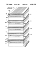
- the laser diode array 110 includes a substrate 42 and several layers 44, 46, 48, 50,52, 54 and 56 with proton implant region 57.
- the active layer 48 in diode array 110 comprises iAl z Ga 1-z As, where z equals zero.
- the diode array 110 includes a plurality of elongated strips. Any number ofstrips can be utilized in the practice of this invention.
- Laser diode array utilizes eleven strips comprising a first strip 112, a second strip 114, a third strip 116, a fourth strip 118, a fifth strip 120, a sixth strip 122, a seventh strip 124, an eighth strip 126, a ninth strip 128, a tenth strip 130 and an eleventh strip 132.
- the width of each of the above strips is substantially the same, ranging from about 2.5 um to about 5 um, preferably about 3.5 um for the gain guided lasers discussed herein.
- Each strip is separated by a resistive material or proton implant region 57 sandwiched between each strip 112, 114, 116, 118, 120, 122, 124, 126, 128,130 and 132.
- the active layer 48 of FIG. 4 includes a left portion 134 and a right portion 136.
- the cross section of active layer 48 perpendicular to the direction of light emission is substantially wedge shaped.
- the thickness of active layer 48 can range from about 20 ⁇ to about 200 ⁇ , but preferably ranges from about 50 ⁇ at left portion 134 to about 70 ⁇ at the right portion 134 thereof.
- the active layer 48 of laser diode array110 is wedged-shaped to provide stable pumping radiation uniformly distributed over a broad bandwidth to a lasant material, thereby providingan improved and more stable laser diode array which provides enhanced stability despite aging and temperature, pressure, and current variations.
- laser diode array 110 is designed so that the active layer adjacent to the middle strip or sixth strip 122 emits radiation at or near the absorption peak of the lasant material, for example, at about 808 nm for neodymium-doped YAG, thereby providing a more stable laser diode array than conventional arrays.
- first emitting strip area 138 having a layer thickness ranging from 48 ⁇ to 52 ⁇ , preferably 50 ⁇
- second strip emitting area 140 having a layer thickness ranging from 50 ⁇ to 54 ⁇ , preferably 52 ⁇
- third strip emitting area 142 having a layer thickness ranging from 52 ⁇ to 56 ⁇ , preferably 54 ⁇
- fourth strip emitting area 144 having a layer thickness rangingfrom 54 ⁇ to 58 ⁇ , preferably 56 ⁇
- a fifth strip emitting area 146 having a layer thickness ranging from 56 ⁇ to 60 ⁇ , preferably 58 ⁇
- a sixth strip emitting area 148 having a layer thickness ranging from 58 ⁇ to 62 ⁇ , preferably 60 ⁇
- a seventh strip emitting area150 having a layer thickness ranging from 60 ⁇ to 64 ⁇ , preferably 62 ⁇
- an eighth strip emitting area 152 having a layer thickness ranging from 62 ⁇ to 66 ⁇ , preferably 64 ⁇
- the wedge-shaped active layer 48 has an upper and lower heterojunction 160 and 162, respectively.
- laser diode array 110 has an emission spectrum as illustrated in the dashed waveform in FIG. 2c, wherein a light is emitted from the first strip emitting area 138 at a wavelength ranging from 803.2 nm to 804.8 nm, preferably 804.0 nm, the second strip emitting area 140 at a wavelength ranging from 804 nm to 805.6 nm, preferably 804.8 nm, the third strip emitting area 142 at a wavelength ranging from 804.8 nm to 806.4 nm, preferably 805.6 nm, the fourth strip emitting area 144 at a wavelength ranging from 805.6 nm to 807.2 nm, preferably 806.4 nm, the fifth strip emitting area 146 at a wavelength ranging from 806.4 nm to 808.0 nm, preferably 807.2 nm, the sixth strip emitting area 148 at a wavelength ranging from 807.2 n
- the sixth strip emitting area 148 layer thickness would be modified so that sixth strip emitting area 148 would emit light at about 806 nm. Accordingly, in such an example, all of the wavelength values given in the preceding paragraph would be decreased by 2nm.
- Laser diode array 164 includes a substrate 42 and layers 44, 46, 48, 50, 52, 54 and 56, with proton implant region 57.
- Active layer 48 includes a left portion 134 and a right portion 136.
- Laser diode array 164 includes a plurality of eleven strips 166, all having the same widths and lengths, each of the lengths coextensive with laser diode array 164.
- the active layer 48 of FIG. 5 includes the formula Al z Ga 1-z As.
- the aluminum content or value of z varies from about 0.0926 at the left portion 134 to about 0.079 at the right portion 136 of active layer 48.
- One approach which has been used in the fabrication of an AlGaAs multiple wavelength light emitting bar or diode is described by J. E. Epler in Appl. Phys. Lett., Vol. 52, No. 18, 1988, pp. 1499-1501.
- the Al composition of the active layer and emission wavelength varies as a function of position along the bar.
- the value of z remains constant, at 7 atomic% or less, and a concentration of an n-type or p-type dopant is varied fromthe left portion 134 to the right portion 136 of active layer 48.
- the value of z or a dopant concentration is varied across active layer 48, to provide a laser diode array for generating optically pumped radiation having a uniform intensity distributed over a broad bandwidth to pump a lasant material, with the absorption band of the lasant material receiving radiation within such bandwidth.
- the active layer 48 includes several emitting areas directly below and adjacent to a plurality of eleven strips 166.
- the active layer 48 includes a first strip emitting area 168, a second strip emitting area 170, a third strip emitting area 172, a fourth strip emitting area 174, a fifth strip emitting area 176, a sixth strip or middle emitting area 178, a seventh strip emitting area 180, an eighth strip emitting area 182, a ninth strip emitting area 184, a tenth strip emitting area 186 and an eleventh strip emitting area 188.
- the first strip emitting area 168 has an aluminum composition or z value in the formula Al z Ga 1-z As ranging from 0.0926 to 0.0904, preferably 0.0916
- the second strip emitting area 170 has a z value ranging from 0.0916 to 0.0892, preferably 0.0904
- the third strip emittingarea 172 has a z value ranging from 0.0904 to 0.0881, preferably 0.0892
- a fourth strip emitting area 174 has a z value ranging from 0.0892 to 0.0869, preferably 0.0881
- a fifth strip emitting area 176 has a z value ranging from 0.0881 to 0.0858, preferably 0.0869
- a sixth strip emitting area 178 has a z value ranging from 0.0869 to 0.0846, preferably 0.0858
- aseventh strip emitting area 180 has a z value ranging from 0.0858 to 0.0834, preferably 0.0846, an eighth strip emitting area 18
- the middle or sixth strip emitting area 178 of active layer 48 is designed to match the absorption peak of the lasant material. For a different absorption peak, the above z values or dopant concentrations would be modified so that the middle strip emitting area 178 would match the absorption peak of the lasant material.
- the concentration of n-type or p-type dopants is varied from the left portion 134 to the right portion 136, of active layer 48.
- the p-type dopants can include magnesium, zinc, cadmium, beryllium, amphoteric dopants, carbon, silicon, germanium, tin, etc. and equivalents thereof.
- the n-type dopants can include tellurium, selenium, sulfur, and the amphoteric dopants, and equivalents thereof.
- the preferredn-type dopants are selenium, tellurium and silicon.
- an impurity that exhibits a donor level and/or an acceptor level, depending on the particular charge state in which it is incorporated is referred to as an amphoteric dopant.
- an amphoteric dopant is a material which can be used as an n-type or p-type dopant to dope a semiconductor, depending on how it is incorporatedinto the material.
- the composition of active region 48 is kept constantat about 0.07 (Al.sub..07 Ga.sub..93 As), but the doping concentration is varied.
- the n-type dopant can range from about 3.8 ⁇ 10 18 /cm 3 at the left portion 134 of active layer 48, to about 7.5 ⁇ 10 18 /cm 3 at the right portion 136 thereof.
- the first strip emitting area 168 includes an n-type dopant ranging from 3.8 ⁇ 10 18 /cm 3 to 4.2 ⁇ 10 18 /cm 3 , preferably 4.0 ⁇ 10 18 /cm 3
- the second strip area170 includes an n-type dopant ranging from 4.0 ⁇ 10 18 /cm 3 to4.5 ⁇ 10 18 /cm 3 , preferably 4.2 ⁇ 10 18 /cm 3
- the third strip emitting area 172 includes an n-type dopant ranging from 4.2 10 18 /cm 3 to 4.7 ⁇ 10 18 /cm 3 , preferably 4.5 ⁇ 10 18 /cm 3
- the fourth strip emitting area 174 includesan n-type dopant ranging from 4.5 ⁇ 10 18 /cm 3 to 5.0 ⁇ 16 18 /cm 3 , preferably 4.7 ⁇ 10 18 /cm 3
- the fifth strip emitting area 176 includes an n-type dopant ranging from 4.7 ⁇ 10 18 /cm 3
- Laser device 200 includes laser diode array 201 which includes a substrate 42 and layers 44, 46, 48, 50, 52, 54 and 56, with proton implant region 57. Directly above and adjacent to laser diode array 201 is a temperature varying means 202.
- the strip emitting area 242 emits light at about 808nm which is the lasant materials absorption peak in this example.
- This structure is designed to operate with ambient temperature ranging from about -30° C. to about +100° C.
- the temperature varying means 202 can be utilized to apply a temperature gradient across the active layer 48 of laser diode array 201, to temperature tune array 201 to emit a plurality of distinct wavelengths, toproduce a multi-wavelength laser diode array or pump which has improved stability despite temperature and current variations.
- the temperature varying means 202 includes a left portion or thermoelectricheater/cooler 204, a right portion or thermoelectric heater/cooler 206 and an intermediate portion or electrically and thermally conductive plate 208.
- the conductive plate 208 is positioned above, adjacent and parallel to the plurality of eleven strips 209 of laser diode array 201. Again, as is understood in the art, any number of strips can be used in the practiceof this invention.
- the strips 209 have approximately equal strip widths andlengths.
- the conductive plate 208 includes a first strip portion 210, a second stripportion 212, a third strip portion 214, a fourth strip portion 216, a fifthstrip portion 218, a sixth strip portion 220, a seventh strip portion 222, an eighth strip portion 224, a ninth strip portion 226, a tenth strip portion 228 and an eleventh strip portion 230. All of the above strip portions are adjacent, elongated and coextensive with the plurality of eleven strips 209 and the laser diode array 201.
- a first temperature is generated by left thermoelectric heater/cooler 204 and a second different temperature applied by right theromoelectric heater/cooler 206 of temperature varying means 202, through conductive plate 208, so as to apply a temperature gradient across the active layer 48, thereby producing light from active layer 48 at a plurality of distinct wavelengths as illustrated in FIG. 2c.
- the temperature coefficient of wavelength in laser device 201 of FIG.6a is approximately 0.27 to 0.3 nm/° C.
- the laser diode array 201 can be temperature tuned so that each strip of the plurality of eleven strips 209 is tuned toa distinct and different wavelength from each strip immediately adjacent thereto, to produce a multi-wavelength laser diode pump, having the characteristics illustrated in the dashed waveform of FIG. 2c.
- the laser diode array 201 effectively provides a source of stable and constant emission at the appropriate absorption wavelength of the lasant material, despite temperature and current variations and fluctuations and aging of the device 201.
- thermoelectric heater/cooler 204 and 206 of temperature varying means 202 each include not only separate and independent thermoelectric heater/coolers, but also independent thermal sensors and feed-back circuits.
- the thermoelectric heater/coolers 204 and206 can each be set and controlled independently, anywhere from about 0° C. to about 60° C.
- thermoelectric heater/coolers 204 and 206 are conventional in nature, and can be monitored using conventional temperature sensors, such as thermocouples, thermistors, etc. When the temperature deviates from a desired value, a voltage is produced in the sensing circuits. The sign of this voltage indicates whether the temperature is warmer or colder than the pre-set null point. Current is automatically supplied in the directionnecessary to correct the temperature drift. Each cooler also includes an adequate heat sink to dissipate and absorb heat in order to maintain the required temperature gradient.
- the active layer 48 includes corresponding strip emitting areas below and adjacent to the above described conductive plate strip portions 210, 212, 214, 216, 218, 220, 222, 224, 226, 228 and 230.
- a first strip emitting area 232 of active layer 48 is directly below and adjacent to first strip portion 210 of conductive plate 208.
- a second strip emitting area 234 of active layer 48 is below and adjacent to second strip portion 212
- a third strip emitting area 236 is below and adjacent to third strip portion 214
- a fourth strip emitting area 238 is below and adjacent to fourth strip portion 216
- a fifth strip emitting area 240 is below and adjacent to fifth strip portion 218,
- a sixth strip emitting area 242 is below and adjacent to sixth strip portion 220
- a seventh strip emitting area 244 is below and adjacent to seventh strip portion 222
- an eighth strip emitting area 246 is below and adjacent to eighth strip portion 224
- a ninth strip emitting area 248 is below and adjacent to ninth strip portion 226, a tenth strip emitting area 250 is below and adjacent to tenth strip portion 228 and an eleventh strip emitting area 252 is below and adjacent to eleventh strip portion 230.
- a temperature versus position graph 254 illustrates the temperature ranges and variations applied to active layer 48 from conductive plate 208, moving from the left to the right side 134 to 136 ofactive layer 48.
- a first position 256 indicates that first strip portion 210 of conductive plate 208, applies a temperature t first strip emitting area 232 of active layer 48 ranging from 6° C. to 11.33° C.,preferably 8.67° C.
- a second position 258 indicates that second strip portion 212 applies a temperature to second strip emitting area 234 ranging from about 8.67° C.
- a third position 260 indicates that third strip portion 214 applies a temperature to third strip emitting area 236 ranging from 11.33° C. to 16.67° C., preferably 14° C.
- a fourth position 262 indicates that fourth strip portion 216 applies a temperature to fourth strip emitting area 238 ranging from 14° C.to 19.33° C., preferably 16.67° C.
- a fifth position 264 indicates that fifth strip portion 218 applies a temperature to fifth strip emitting area 240 ranging from 16.67° C.
- a sixth position 266 indicates that middle orsixth strip portion 220 applies a temperature to sixth strip emitting area 242 ranging from 19.33° C. to 24.6° C., preferably 22° C.
- a seventh position 268 indicates that seventh strip portion222 applies a temperature to seventh strip emitting area 244 ranging from 22° C. to 27.33° C., preferably 24.67° C.
- an eighth position 270 indicates that eighth strip portion 224 applies a temperatureto eighth strip emitting area 246 ranging from 24.67° C.
- a ninth strip position 272 indicates that ninth strip portion 226 applies a temperature to ninth strip emitting area 248 ranging from 27.33° C. to 32.67° C.,preferably 30° C.
- a tenth strip position 274 indicates that tenth strip portion 228 applies a temperature to tenth strip emitting area 250 ranging from 30° C. to 35.33° C., preferably 32.64° C.
- an eleventh strip position 276 indicates that eleventh strip portion 230 applies a temperature to eleventh strip emitting area 252 ranging from 32.68° C. to 38° C., preferably 35.33° C. under operating and lasing conditions (See Table 2).
- the device 200 is designed so that the middle or sixth strip 242 when operating and lasing, emits a light matching the absorption window or peakof the lasant material, thereby enhancing stability despite temperature andpressure variations and aging of device 200, similar in many respects to arrays 40, 110 and 164 in FIGS. 3, 4 and 5, respectively.
- the middle or sixth strip emitting area 242 emits light under lasing conditions at about the lasant materials absorption peak.
- the preferred temperatures would be modified so that the middle strip emitting area 242 would match the absorption peak.
- FIG. 7 there is schematically shown another laser diode array 290 whichis suitable for use in the practice of this invention.
- the laser diode array 290 can have any number of active layers, however the array 290 in FIG. 7 only illustrates five such layers.
- At the bottom of laser diode array 290 is n+GaAs substrate 292 with a plurality of layers stacked abovein the following order: n Al x Ga l-x As layer 294, Al y Ga l-y As barrier 296, Al z Ga l-z As fifth active layer 298, Al y Ga l-y As barrier 300, Al z4 Ga l-z4 As fourth activelayer 302, Al y Ga l-y As barrier 304, Al z3 Ga l-z3 As third active layer 306, Al y Ga l-y As barrier 308, Al z2 Ga l-z2 As second active layer 310, Al y Ga l-y As barrier 312, Al zl Ga l-zl As first active layer 31
- the first and second examples of laser diode array 290 in FIG. 7, are similar in many respects to the laser diode array 164 in FIG. 5.
- the bandwidth of laser diode array 290 is about 5 nm wide, and is more stable despite temperature and current variations and fluctuations than conventional laser diode arrays, because of the wide bandwidth.
- Laser diode array 290 eases and relaxes the requirements of wavelength matching between the laser diode array and the absorption band of the lasant material, which also provides a stable output radiation from the lasant material.
- the characteristics of conventional laser diode arrays change and drift after several hours of lasing, which makes it moredifficult to apply radiation at the appropriate absorption peak of the lasant material.
- Laser diode array 290 only has one elongated strip 326, having a width ranging from about 50 um to 150 um, preferably 100 um.
- Strip 326 is coextensive with and runs the length of laser diode array 290, typically, about 400 um long.
- Active layers 298, 302, 306, 310 and 314 each have a center area 328, 330, 332, 334 and 336, respectively, which produce or emit light under lasing conditions at different or distinct wavelengths.
- the fifth active layer 298 value of z5 in Al z5 Ga l-z5 As ranges fromabout 0.0846 to 0.0823, preferably 0.0834
- the value of z4 in fourth activelayer 302 ranges from about 0.0834 to 0.0858, preferably 0.0846
- the value of z3 in third active layer 306 ranges from about 0.0846 to 0.0869, preferably 0.0858
- the value of z2 in the second active layer 310 ranges from about 0.0858 to 0.0881, preferably 0.0869
- the value of z1 in first active layer 314 ranges from about 0.0869 to 0.0892, preferably 0.0881, but are not limited to such ranges.
- the bandwidth of laser diode array 290 is about 5 nm wide. If, for example,the absorption peak of the lasant material is at about 808 nm, then the wavelength emitted for fifth active layer 298, fourth active layer 302, third active layer 306, second active layer 310, and first active layer 314, are adjusted to about 809.6 nm, 808.8 nm, 808.0 nm, 807.2 nm and 806.4 nm, respectively by appropriate selection of the composition for each layer.
- the bandwidth of laser device 290 is about half as wide as that illustrated in the dashed waveform of FIG. 2c. The intensity of the pumping radiation in laser device 290 would however be uniformly distributed across such bandwidth.
- the values of z5, z4, z3, z2, and z1 are constant at about 0.07, and the concentration of n-type dopants include about 5.9, 5.6, 5.3, 5.0 and 4.7 ⁇ 10 18 /cm 3 in active layers 298, 302, 306, 310 and 314, respectively, each of the above active layers producing and emitting light at about the same wavelengths and uniform distribution, as discussed in the preceding paragraph.
- FIG. 8 illustrates yet another laser diode array 340 which is suitable for use in the practice of the instant invention.
- Laser diode array 340 includes substrate 292, layer 294, barrier 296, fifth active layer 342, barrier 300, fourth active layer 344, barrier 304, third active layer 346,barrier 308, second active layer 348, barrier 312, first active layer 350, barrier 316, layer 318, layer 320, and layer 322, with proton implant region 324, however, any number of active layers may be used in the practice of this invention.
- the elongated strip 326 is coextensive with and spans the length of array 340.
- Active layers 342, 344, 346, 348, and 350 comprise GaAs.
- Each active layer has a different layer thickness than each adjacent active layer, and each emits a light at a distinct wavelength from center areas 352, 354, 356, 358, and 360, respectively, under lasing conditions, to produce laser light which is more stable than conventional laser diode arrays, despite temperature and current variations.
- the fifth active layer 342 thickness ranges from 62 ⁇ to 66 ⁇ , preferably 64 ⁇ emitting light having a wavelengthof about 809.6 nm
- the fourth active layer thickness 344 ranges from 60 ⁇ to 64 ⁇ , preferably 62 ⁇ , emitting light having a wavelengthof about 808.8 nm
- the third active layer thickness 346 ranges from 58 ⁇ to 62 ⁇ , preferably 60 ⁇ , emitting light having a wavelength of about808.0 nm, (assuming the absorption peak of the lasant material is at about 808 nm)
- the second active layer thickness 348 ranges from 56 ⁇ to 60 ⁇ , preferably 58 ⁇ , emitting light having a wavelength of about 807.2 nm
- the first active layer thickness 350 ranges from 54 ⁇ to 58 ⁇ , preferably 56 ⁇ , emitting light having a wavelength of about 806.4 nm under lasing conditions.
- the thickness of the above active layers vary in a manner similar to the variation of thicknesses in the strips in FIG. 3.
- FIG. 9 is another laser diode array 366, similar in many waysto the laser diode array 290 in FIG. 7.
- the laser diode array 366 in FIG. 9 includes substrate 292 and layers 294, 296, 298, 300, 302, 304, 306, 308, 310, 312, 314, 316, 318, 320, and 322 and proton implant area 324. These layers are the same as those illustrated in FIG. 7.
- the value of z5, z4, z3, z2, and z1 in each active layer 298, 302, 306, 310 and 314 can vary.
- FIG. 9 is another laser diode array 366, similar in many waysto the laser diode array 290 in FIG. 7.
- the laser diode array 366 in FIG. 9 includes substrate 292 and layers 294, 296, 298, 300, 302, 304, 306, 308, 310, 312, 314, 316, 318, 320, and 322 and proton implant area 324. These layers are the same as those illustrated in
- n-type or p-type dopants can be incorporated into each active layer at various concentrations.
- the value of z and dopant concentrations vary in order to produce a substantially uniform radiation over a broad bandwidth, thereby providing a laser diode array with enhanced stability despite aging and temperature, and current variations.
- the laser device 366 includes a plurality of 11 strips 368. However, any number of strips may be utilized in the practice of this invention.
- the fifth active layer 298, emits light ranging from about 808.8 nm to about 810.4 nm, preferably 809.6 nm, at strip area 370 below and adjacent to strips 368
- the fourth active layer 302 emits light ranging from about 808.0 nm to about 809.6 nm, preferably 808.8 nm, at strip area 372 below and adjacent to strips 368
- the third active layer 306 emits light rangingfrom about 807.2 nm to 808.8 nm, preferably 808.0 nm, at strip area 374 below and adjacent to strips 368
- the second layer 310 emits light rangingfrom about 806.4 nm to 808.0 nm, preferably 807.2 nm, at strip area 376 below and adjacent to strips 368
- the first active layer 314 emits light ranging from about 805.6 nm to 807.2 nm,
- the values of z5, z4, z3, z2 and z1 of active layers 298, 302, 306, 310, and 314, respectively, are the same as previously discussed with respect to the first embodiment of laser diode array 290 in FIG. 7, for example about 0.0834, 0.0846, 0.0858, 0.0869 and 0.0881, respectively.
- the concentrations of n-type dopants in active layers 298, 302, 306, 310 and 314, are the same as those previouslydiscussed with respect to the second embodiment of laser diode array 290 inFIG. 7, for example, 5.9, 5.6, 5.3, 5.0 and 4.7 ⁇ 10 18 cm 3 , respectively.
- FIG. 10 is yet another laser diode array which is suitable for use in the practice of the instant invention, and is similar in many respects to the laser diode array 40 of FIG. 8.
- a laser diode array 384 isshown which includes a substrate 292, and layers 294, 296, 86, 304, 388, 308, 390, 312, 392, 316, 318, 320 and 322, with a proton implant region 324.
- the above layers are the same as those illustrated in FIG. 8.
- Laser diode array 384 active layers 386, 388, 390 and 329 vary in thickness so that under lasing conditions, a substantially uniform radiation over a broad bandwidth is produced, thereby providing a laser diode array with enhanced stability despite temperature and current variations.
- the fourth active layer 386 of laser diode array 384 is wider or thicker than the third active layer 388.
- the third active layer 388 is wider or thicker than the second active layer 390, and the second active layer 390 is wider or thicker than the first active layer 392.
- the fourth active layer 386 thickness ranges from 64 ⁇ to 60 ⁇ , preferably 62 ⁇
- the third active layer thickness from 62 ⁇ to 58 ⁇
- the second active layer 390 ranges from 60 ⁇ to 56 ⁇ , preferably 58 ⁇
- the first active layer 382 ranges from 58 ⁇ to 54 ⁇ , preferably 56 ⁇ .
- Each active layer of laser device 384 comprises GaAs.
- strip area 394 of active layer 386 emits light below and adjacent to the plurality of strip 368 at about 809.6 nm
- strip area 396 of the third active layer 388 emits light at about 808.8 nm
- strip area 398 of the second active layer 390 emits light at about 808 nm
- the strip area 400 of the first active layer 392 emits light at about 807.2 nm, assuming the lasant material absorption peak is at about 808.5 nm.
- the thicknesses of the active layers in laser device 384 vary in a manner similar to the variation of the strip thicknesses in laser diode array 40 of FIG. 3.
- FIG. 11 illustrates an alternate laser diode array which is also suitable for use in the practice of the subject invention. It will be appreciated, that any number of laser devices each with any number of strips can be utilized in the practice of this invention.
- a hybrid laser diode array 406 is shown which includes a fifth laser device 408 at the bottom, a fourth laser device 410, a third laser device 412, a second laser device 414, and a first laser device 416 at the top.
- the fifth laser device 408 includes a substrate 418 and layers 420, 422, 424, fifth active layer 426, layer 428,430, and 432 with a proton implant region 434, and a plurality of strips 436 having the same width.
- the fourth, third, second and first laser devices 410, 412, 414 and 416 include similar layers, except that each has a different active layer.
- the hybrid laser diode array 406 Under lasing conditions, the hybrid laser diode array 406 generates opticalpumping radiation having a uniform intensity distributed over a broad bandwidth for pumping the absorption band of a lasant material.
- the intensity in the hybrid laser diode array 406 is greater than in the previous laser diode arrays, and can be easily maintained because of easy access to devices 408, 410, 412, 414 and 416 and efficiently mass produced.
- the fourth laser device 410 includes a fourth active layer 438
- the third laser device 412 includes a third active layer 440
- the second laser device 414 includes a second active layer 442
- first laser device 416 includes a first active layer 444.
- each laser device 408, 410, 412, 414, and 416 are fourth space 446, third space 448, second space 450, and first space 452, respectively.
- Each active layer in each laser device includes a strip area 454, 456, 458,460 and 462, adjacent to and below the plurality of strips 436 of each device.
- the hybrid laser device has a bandwidth of about 5 nm wide.
- Strip area 454 emits light from fifth active layer 424 ranging from about 808.8 nm to about 810.4 nm, preferably 809.6 nm
- strip area 456 emits light ranging from about 808.0 nm to about 809.6 nm, preferably 808.8 nm from active layer 438
- strip area 458 emits light ranging from about 807.2 nm to about 808.8 nm, preferably 808.0 nm from active layer 440
- strip area 460 emits light ranging from about 806.4 nm to about 808.0 nm, preferably 807.2 nm from active layer 442
- strip area 462 emits light ranging from about 805.6 nm to 807.2nm, preferably 806.4 nm from active layer 444 under lasing conditions.
- Devices 408, 410, 412, 414 and 416 can be temperature tuned in a manner similar in many respects to that disclosed with respect to laser device 200 in FIG. 6a, by tuning each such device at a different temperature, thealuminum concentration and doping can be varied in active layers 424, 438, 440, 442 and 444, in a manner similar in many respects to that discussed in connection with FIGS. 5, 7, or 9, the active layer thickness in each can be varied in a manner similar to that discussed in connection with FIGS. 8 and 10, the strip width can be varied as illustrated in FIG. 3, and/or each device can be pressure tuned, or any combination thereof.
Abstract
Description
              TABLE 1
______________________________________
                                    2nd Ex.
                                    of FIG. 5,
                            lst Ex. z approx. .07
                            of FIG. 5
                                    Preferred
Active Layer                Preferred
                                    n-type
48 Strip  Item    Wave      Value of
                                    dopant
Emitting  No. in  Length    z in    concent.
Area      FIG. 5  (in nm)   Al.sub.z Ga.sub.z-1 As
                                    (× 10.sup.18 /cm.sup.3)
______________________________________
 1st      168     804.0     .0916   4.0
 2nd      170     804.8     .0904   4.2
 3rd      172     805.6     .0892   4.5
 4th      174     806.4     .0881   4.7
 5th      176     807.2     .0869   5.0
 6th      178     808.0     .0858   5.3
 7th      180     808.8     .0846   5.6
 8th      182     809.6     .0834   5.9
 9th      184     810.4     .0823   6.2
10th      186     811.2     .0811   6.6
llth      188     812.0     .0800   7.0
______________________________________
              TABLE 2
______________________________________
Active Layer 48
              Preferred
Strip Emitting Area
              Emission       Preferred
Item No.      Wavelength     Temperature
______________________________________
1       232       804.0          8.67° C.
2       234       804.8          11.33° C.
3       236       805.6          14° C.
4       238       806.4          16.67° C.
5       240       807.2          19.33° C.
6       242       808.0          22° C.
7       244       808.8          24.67° C.
8       246       809.6          27.33° C.
9       248       810.4          30° C.
10      250       811.2          32.67° C.
11      252       812.0          35.33° C.
______________________________________
Claims (27)
Priority Applications (7)
| Application Number | Priority Date | Filing Date | Title |
|---|---|---|---|
| US07/221,670 US4901330A (en) | 1988-07-20 | 1988-07-20 | Optically pumped laser |
| DE68913614T DE68913614T2 (en) | 1988-07-20 | 1989-07-18 | Optically pumped laser. |
| EP89307249A EP0352059B1 (en) | 1988-07-20 | 1989-07-18 | An optically pumped laser |
| AT89307249T ATE102755T1 (en) | 1988-07-20 | 1989-07-18 | OPTICALLY PUMPED LASER. |
| KR1019890010256A KR910003877A (en) | 1988-07-20 | 1989-07-20 | Optical pump laser |
| AU38297/89A AU3829789A (en) | 1988-07-20 | 1989-07-20 | An optically pumped laser |
| JP1188666A JPH0254982A (en) | 1988-07-20 | 1989-07-20 | Light pumping type laser |
Applications Claiming Priority (1)
| Application Number | Priority Date | Filing Date | Title |
|---|---|---|---|
| US07/221,670 US4901330A (en) | 1988-07-20 | 1988-07-20 | Optically pumped laser |
Publications (1)
| Publication Number | Publication Date |
|---|---|
| US4901330A true US4901330A (en) | 1990-02-13 |
Family
ID=22828817
Family Applications (1)
| Application Number | Title | Priority Date | Filing Date |
|---|---|---|---|
| US07/221,670 Expired - Fee Related US4901330A (en) | 1988-07-20 | 1988-07-20 | Optically pumped laser |
Country Status (7)
| Country | Link |
|---|---|
| US (1) | US4901330A (en) |
| EP (1) | EP0352059B1 (en) |
| JP (1) | JPH0254982A (en) |
| KR (1) | KR910003877A (en) |
| AT (1) | ATE102755T1 (en) |
| AU (1) | AU3829789A (en) |
| DE (1) | DE68913614T2 (en) |
Cited By (65)
| Publication number | Priority date | Publication date | Assignee | Title |
|---|---|---|---|---|
| US5022043A (en) * | 1989-12-20 | 1991-06-04 | Spectra-Physics | High power diode-pumped solid state laser with unstable resonator |
| US5077750A (en) * | 1989-05-30 | 1991-12-31 | Thompson-Csf | Power lasers pumped by laser diodes |
| US5081637A (en) * | 1989-11-28 | 1992-01-14 | Massachusetts Institute Of Technology | Multiple-laser pump optical system |
| US5090019A (en) * | 1991-01-10 | 1992-02-18 | The United States Of America As Represented By The Secretary Of The Navy | Laser diode-pumped tunable solid state laser |
| US5119394A (en) * | 1991-02-13 | 1992-06-02 | The United States Of America As Represented By The Secretary Of The Navy | Technique for longitudinal optical pumping of a laser |
| US5124999A (en) * | 1988-09-13 | 1992-06-23 | Fuji Photo Film Co., Ltd. | Laser-diode-pumped solid-state laser |
| US5138624A (en) * | 1989-11-16 | 1992-08-11 | The Boeing Company | Multiwavelength LED and laser diode optical source |
| US5163058A (en) * | 1990-06-01 | 1992-11-10 | The General Electric Company, P.L.C | Semiconductor laser pump source |
| US5170406A (en) * | 1991-03-13 | 1992-12-08 | Amoco Corporation | High-power, end-pumped solid state laser |
| US5185758A (en) * | 1989-11-28 | 1993-02-09 | Massachusetts Institute Of Technology | Multiple-laser pump optical system |
| US5265116A (en) * | 1988-02-02 | 1993-11-23 | Massachusetts Institute Of Technology | Microchip laser |
| US5285467A (en) * | 1991-06-17 | 1994-02-08 | The United States Of America As Represented By The Secretary Of The Navy | Compact, efficient, scalable neodymium laser co-doped with activator ions and pumped by visible laser diodes |
| US5289482A (en) * | 1992-12-30 | 1994-02-22 | The United States Of America As Represented By The Secretary Of The Navy | Intracavity-pumped 2.1 μm Ho3+ :YAG laser |
| US5319528A (en) * | 1990-08-01 | 1994-06-07 | Diomed Limited | High power light source |
| US5351259A (en) * | 1991-10-24 | 1994-09-27 | Mitsubishi Denki Kabushiki Kaisha | Semiconductor laser-pumped solid-state laser with plural beam output |
| US5365368A (en) * | 1992-08-28 | 1994-11-15 | Hughes Aircraft Company | Efficient bi-directional optical fiber amplifier for missile guidance data link repeater |
| US5457706A (en) * | 1993-03-30 | 1995-10-10 | The United States Of America As Represented By The Administrator Of The National Aeronautics And Space Administration | Tunable CW diode-pumped Tm,Ho:YLiF4 laser operating at or near room temperature |
| US5734672A (en) * | 1996-08-06 | 1998-03-31 | Cutting Edge Optronics, Inc. | Smart laser diode array assembly and operating method using same |
| US5898211A (en) * | 1996-04-30 | 1999-04-27 | Cutting Edge Optronics, Inc. | Laser diode package with heat sink |
| US5913108A (en) * | 1998-04-30 | 1999-06-15 | Cutting Edge Optronics, Inc. | Laser diode packaging |
| US5936984A (en) * | 1997-05-21 | 1999-08-10 | Onxy Optics, Inc. | Laser rods with undoped, flanged end-caps for end-pumped laser applications |
| US6061378A (en) * | 1997-05-13 | 2000-05-09 | Cutting Edge Optronics, Inc. | Multiple resonant cavity solid-state laser |
| US6222577B1 (en) * | 1999-01-26 | 2001-04-24 | Presstek, Inc. | Multiple-beam, diode-pumped imaging system |
| US6339607B1 (en) | 1999-10-29 | 2002-01-15 | E2O Communications, Inc. | Method and apparatus for modulated integrated optically pumped vertical cavity surface emitting lasers |
| US6347101B1 (en) * | 1998-04-16 | 2002-02-12 | 3D Systems, Inc. | Laser with absorption optimized pumping of a gain medium |
| US20030002545A1 (en) * | 2001-07-02 | 2003-01-02 | Wenbin Jiang | Method and apparatus for wavelength tuning of optically pumped vertical cavity surface emitting lasers |
| US20030058898A1 (en) * | 2001-09-17 | 2003-03-27 | Bernard Beier | Multibeam laser light source with variable laser light source spacing for setting images on printing forms |
| US6553048B2 (en) | 1999-10-29 | 2003-04-22 | E2O Communications, Inc. | Modulated integrated optically pumped vertical cavity surface emitting lasers |
| US6556610B1 (en) | 2001-04-12 | 2003-04-29 | E20 Communications, Inc. | Semiconductor lasers |
| US6636538B1 (en) | 1999-03-29 | 2003-10-21 | Cutting Edge Optronics, Inc. | Laser diode packaging |
| US6700913B2 (en) | 2001-05-29 | 2004-03-02 | Northrop Grumman Corporation | Low cost high integrity diode laser array |
| US20040173788A1 (en) * | 2003-03-06 | 2004-09-09 | Toshiyuki Takizawa | P-type semiconductor and semiconductor metero material and manufacturing methods thereof |
| US6813302B1 (en) * | 2001-08-03 | 2004-11-02 | Coherent Technologies, Inc. | Eyesafe Q-switched Er-doped solid-state laser |
| US20040236203A1 (en) * | 2003-05-19 | 2004-11-25 | Francesco Di Salvo | Silver alloys for use in medical, surgical and microsurgical instruments and process for producing the alloys |
| US20040258123A1 (en) * | 2003-06-23 | 2004-12-23 | Zamel James Michael | Diode-pumped solid-state laser gain module |
| US20050018742A1 (en) * | 2003-07-24 | 2005-01-27 | Hall Daniel F. | Cast laser optical bench |
| DE19883013B4 (en) * | 1998-11-19 | 2005-08-25 | Mitsubishi Denki K.K. | Semiconductor laser excited solid state laser |
| US20060171428A1 (en) * | 2005-02-03 | 2006-08-03 | Pd-Ld, Inc. | High-power, phased-locked, laser arrays |
| US20060203866A1 (en) * | 2005-03-10 | 2006-09-14 | Northrop Grumman | Laser diode package with an internal fluid cooling channel |
| US20070100330A1 (en) * | 2005-11-03 | 2007-05-03 | Luxon, Inc. | Surgical laser systems for soft and hard tissue and methods of use thereof |
| US20070160101A1 (en) * | 2005-09-29 | 2007-07-12 | Osram Opto Semiconductors Gmbh | Laser diode apparatus, laser arrangement having at least one laser diode apparatus, and optically pumped laser |
| US20080025357A1 (en) * | 2006-07-26 | 2008-01-31 | Northrop Grumman Corporation | Microchannel cooler for high efficiency laser diode heat extraction |
| US20080056314A1 (en) * | 2006-08-31 | 2008-03-06 | Northrop Grumman Corporation | High-power laser-diode package system |
| US20080063021A1 (en) * | 2006-09-12 | 2008-03-13 | Samsung Electronics Co., Ltd. | Multibeam laser apparatus and image forming device using the same |
| US20080089380A1 (en) * | 2006-09-28 | 2008-04-17 | Osram Opto Semiconductors Gmbh | Laser arrangement and semiconductor laser for optically pumping a laser |
| US20090185593A1 (en) * | 2008-01-18 | 2009-07-23 | Northrop Grumman Space & Mission Systems Corp. | Method of manufacturing laser diode packages and arrays |
| US20100183039A1 (en) * | 2009-01-21 | 2010-07-22 | Coherent, Inc. | Two-dimensional diode-laser array with broad-band output |
| US20110026551A1 (en) * | 2009-07-28 | 2011-02-03 | Northrop Grumman Systems Corp. | Laser Diode Ceramic Cooler Having Circuitry For Control And Feedback Of Laser Diode Performance |
| US8937976B2 (en) | 2012-08-15 | 2015-01-20 | Northrop Grumman Systems Corp. | Tunable system for generating an optical pulse based on a double-pass semiconductor optical amplifier |
| US9185786B2 (en) | 2006-03-31 | 2015-11-10 | Energetiq Technology, Inc. | Laser-driven light source |
| US20150357516A1 (en) * | 2010-04-12 | 2015-12-10 | Osram Opto Semiconductors Gmbh | Light-Emitting Diode Chip with Current Spreading Layer |
| US9576785B2 (en) | 2015-05-14 | 2017-02-21 | Excelitas Technologies Corp. | Electrodeless single CW laser driven xenon lamp |
| US9590388B2 (en) | 2011-01-11 | 2017-03-07 | Northrop Grumman Systems Corp. | Microchannel cooler for a single laser diode emitter based system |
| US9678262B2 (en) | 2013-09-20 | 2017-06-13 | Qloptiq Photonics GmbH & Co. KG | Laser-operated light source |
| US20170235151A1 (en) * | 2016-02-16 | 2017-08-17 | Gerald Ho Kim | Two-Dimensional Coherent Beam Combination Using Circular Or Spiral Diffraction Grating |
| US9741553B2 (en) | 2014-05-15 | 2017-08-22 | Excelitas Technologies Corp. | Elliptical and dual parabolic laser driven sealed beam lamps |
| US9748086B2 (en) | 2014-05-15 | 2017-08-29 | Excelitas Technologies Corp. | Laser driven sealed beam lamp |
| US9846410B2 (en) * | 2011-09-14 | 2017-12-19 | Intel Corporation | Holographic display systems and methods having elliposidial arrangment of DMD arrays emitting infrared laser radiation |
| US10008378B2 (en) | 2015-05-14 | 2018-06-26 | Excelitas Technologies Corp. | Laser driven sealed beam lamp with improved stability |
| US10057973B2 (en) | 2015-05-14 | 2018-08-21 | Excelitas Technologies Corp. | Electrodeless single low power CW laser driven plasma lamp |
| US10078167B2 (en) | 2013-09-20 | 2018-09-18 | Asml Netherlands B.V. | Laser-operated light source |
| US10109473B1 (en) | 2018-01-26 | 2018-10-23 | Excelitas Technologies Corp. | Mechanically sealed tube for laser sustained plasma lamp and production method for same |
| US10186416B2 (en) | 2014-05-15 | 2019-01-22 | Excelitas Technologies Corp. | Apparatus and a method for operating a variable pressure sealed beam lamp |
| CN114300938A (en) * | 2021-12-30 | 2022-04-08 | 北京工业大学 | Microcavity semiconductor laser on photon cascade GaAs-OI substrate and preparation method |
| US11355898B2 (en) * | 2017-10-30 | 2022-06-07 | Bae Systems Plc | Laser diode array |
Families Citing this family (10)
| Publication number | Priority date | Publication date | Assignee | Title |
|---|---|---|---|---|
| JPH07112083B2 (en) * | 1990-06-14 | 1995-11-29 | 新日本製鐵株式会社 | Array semiconductor laser Edge-pumped solid-state laser |
| JPH07112085B2 (en) * | 1990-07-20 | 1995-11-29 | 新日本製鐵株式会社 | Array semiconductor laser pumped solid-state laser device |
| JPH07112084B2 (en) * | 1990-07-20 | 1995-11-29 | 新日本製鐵株式会社 | Array semiconductor laser pumped solid-state laser device |
| DE19617711A1 (en) * | 1996-02-07 | 1997-08-14 | Fraunhofer Ges Forschung | Optically pumped amplifier, especially a solid state amplifier |
| DE19935998B4 (en) * | 1999-07-30 | 2007-10-18 | Osram Opto Semiconductors Gmbh | Multiple semiconductor laser structure with narrow wavelength distribution |
| WO2002005038A2 (en) * | 2000-07-10 | 2002-01-17 | Corporation For Laser Optics Research | Systems and methods for speckle reduction through bandwidth enhancement |
| JP2003198018A (en) * | 2001-12-28 | 2003-07-11 | Communication Research Laboratory | Light stimulated solid-state laser oscillator |
| DE60309313T2 (en) | 2003-08-11 | 2007-08-30 | Lumera Laser Gmbh | Solid state laser pumped by a laser diode with a convergent bundle |
| JP2011127529A (en) * | 2009-12-18 | 2011-06-30 | National Institutes Of Natural Sciences | Solid-state laser device for engine ignition by semiconductor laser excitation |
| GB2497107B (en) * | 2011-11-30 | 2014-01-08 | Thales Holdings Uk Plc | Laser pumping system |
Citations (2)
| Publication number | Priority date | Publication date | Assignee | Title |
|---|---|---|---|---|
| US4751711A (en) * | 1985-08-16 | 1988-06-14 | Spectra Diode Laboratories, Inc. | Asymmetric offset stripe laser for emission in a single lobe |
| US4791631A (en) * | 1987-08-31 | 1988-12-13 | International Business Machines Corporation | Wide tolerance, modulated blue laser source |
-
1988
- 1988-07-20 US US07/221,670 patent/US4901330A/en not_active Expired - Fee Related
-
1989
- 1989-07-18 AT AT89307249T patent/ATE102755T1/en not_active IP Right Cessation
- 1989-07-18 EP EP89307249A patent/EP0352059B1/en not_active Expired - Lifetime
- 1989-07-18 DE DE68913614T patent/DE68913614T2/en not_active Expired - Fee Related
- 1989-07-20 AU AU38297/89A patent/AU3829789A/en not_active Abandoned
- 1989-07-20 JP JP1188666A patent/JPH0254982A/en active Pending
- 1989-07-20 KR KR1019890010256A patent/KR910003877A/en not_active Application Discontinuation
Patent Citations (2)
| Publication number | Priority date | Publication date | Assignee | Title |
|---|---|---|---|---|
| US4751711A (en) * | 1985-08-16 | 1988-06-14 | Spectra Diode Laboratories, Inc. | Asymmetric offset stripe laser for emission in a single lobe |
| US4791631A (en) * | 1987-08-31 | 1988-12-13 | International Business Machines Corporation | Wide tolerance, modulated blue laser source |
Cited By (117)
| Publication number | Priority date | Publication date | Assignee | Title |
|---|---|---|---|---|
| US5365539A (en) * | 1988-02-02 | 1994-11-15 | Massachusetts Institute Of Technology | Microchip laser |
| US5265116A (en) * | 1988-02-02 | 1993-11-23 | Massachusetts Institute Of Technology | Microchip laser |
| US5124999A (en) * | 1988-09-13 | 1992-06-23 | Fuji Photo Film Co., Ltd. | Laser-diode-pumped solid-state laser |
| US5077750A (en) * | 1989-05-30 | 1991-12-31 | Thompson-Csf | Power lasers pumped by laser diodes |
| US5138624A (en) * | 1989-11-16 | 1992-08-11 | The Boeing Company | Multiwavelength LED and laser diode optical source |
| US5185758A (en) * | 1989-11-28 | 1993-02-09 | Massachusetts Institute Of Technology | Multiple-laser pump optical system |
| US5081637A (en) * | 1989-11-28 | 1992-01-14 | Massachusetts Institute Of Technology | Multiple-laser pump optical system |
| US5022043A (en) * | 1989-12-20 | 1991-06-04 | Spectra-Physics | High power diode-pumped solid state laser with unstable resonator |
| US5163058A (en) * | 1990-06-01 | 1992-11-10 | The General Electric Company, P.L.C | Semiconductor laser pump source |
| US5463534A (en) * | 1990-08-01 | 1995-10-31 | Diomed Limited | High power light source |
| US5319528A (en) * | 1990-08-01 | 1994-06-07 | Diomed Limited | High power light source |
| US5090019A (en) * | 1991-01-10 | 1992-02-18 | The United States Of America As Represented By The Secretary Of The Navy | Laser diode-pumped tunable solid state laser |
| US5119394A (en) * | 1991-02-13 | 1992-06-02 | The United States Of America As Represented By The Secretary Of The Navy | Technique for longitudinal optical pumping of a laser |
| US5170406A (en) * | 1991-03-13 | 1992-12-08 | Amoco Corporation | High-power, end-pumped solid state laser |
| US5285467A (en) * | 1991-06-17 | 1994-02-08 | The United States Of America As Represented By The Secretary Of The Navy | Compact, efficient, scalable neodymium laser co-doped with activator ions and pumped by visible laser diodes |
| US5351259A (en) * | 1991-10-24 | 1994-09-27 | Mitsubishi Denki Kabushiki Kaisha | Semiconductor laser-pumped solid-state laser with plural beam output |
| US5365368A (en) * | 1992-08-28 | 1994-11-15 | Hughes Aircraft Company | Efficient bi-directional optical fiber amplifier for missile guidance data link repeater |
| US5289482A (en) * | 1992-12-30 | 1994-02-22 | The United States Of America As Represented By The Secretary Of The Navy | Intracavity-pumped 2.1 μm Ho3+ :YAG laser |
| US5457706A (en) * | 1993-03-30 | 1995-10-10 | The United States Of America As Represented By The Administrator Of The National Aeronautics And Space Administration | Tunable CW diode-pumped Tm,Ho:YLiF4 laser operating at or near room temperature |
| US5898211A (en) * | 1996-04-30 | 1999-04-27 | Cutting Edge Optronics, Inc. | Laser diode package with heat sink |
| US5985684A (en) * | 1996-04-30 | 1999-11-16 | Cutting Edge Optronics, Inc. | Process for manufacturing a laser diode having a heat sink |
| US5734672A (en) * | 1996-08-06 | 1998-03-31 | Cutting Edge Optronics, Inc. | Smart laser diode array assembly and operating method using same |
| US6385226B2 (en) | 1996-08-06 | 2002-05-07 | Trw Inc. | Smart laser diode array assembly |
| US6272164B1 (en) | 1996-08-06 | 2001-08-07 | Cutting Edge Optronics, Inc. | Smart laser diode array assembly |
| US6144684A (en) * | 1996-08-06 | 2000-11-07 | Cutting Edge Optronics, Inc. | Smart laser diode array assembly |
| US6061378A (en) * | 1997-05-13 | 2000-05-09 | Cutting Edge Optronics, Inc. | Multiple resonant cavity solid-state laser |
| US5936984A (en) * | 1997-05-21 | 1999-08-10 | Onxy Optics, Inc. | Laser rods with undoped, flanged end-caps for end-pumped laser applications |
| US6347101B1 (en) * | 1998-04-16 | 2002-02-12 | 3D Systems, Inc. | Laser with absorption optimized pumping of a gain medium |
| US6310900B1 (en) | 1998-04-30 | 2001-10-30 | Cutting Edge Optronics, Inc. | Laser diode package with heat sink |
| US5913108A (en) * | 1998-04-30 | 1999-06-15 | Cutting Edge Optronics, Inc. | Laser diode packaging |
| DE19883013B4 (en) * | 1998-11-19 | 2005-08-25 | Mitsubishi Denki K.K. | Semiconductor laser excited solid state laser |
| US6222577B1 (en) * | 1999-01-26 | 2001-04-24 | Presstek, Inc. | Multiple-beam, diode-pumped imaging system |
| US7361978B2 (en) | 1999-03-29 | 2008-04-22 | Northrop Gruman Corporation | Laser diode packaging |
| US6636538B1 (en) | 1999-03-29 | 2003-10-21 | Cutting Edge Optronics, Inc. | Laser diode packaging |
| US20060186500A1 (en) * | 1999-03-29 | 2006-08-24 | Stephens Edward F | Laser diode packaging |
| US7060515B2 (en) | 1999-03-29 | 2006-06-13 | Cutting Edge Optronics, Inc. | Method of manufacturing a laser diode package |
| US20040082112A1 (en) * | 1999-03-29 | 2004-04-29 | Stephens Edward F. | Laser diode packaging |
| US6424669B1 (en) | 1999-10-29 | 2002-07-23 | E20 Communications, Inc. | Integrated optically pumped vertical cavity surface emitting laser |
| US6940885B1 (en) | 1999-10-29 | 2005-09-06 | Jds Uniphase Corporation | Systems, methods, and apparatuses for optically pumped vertical cavity surface emitting laser devices |
| US6339607B1 (en) | 1999-10-29 | 2002-01-15 | E2O Communications, Inc. | Method and apparatus for modulated integrated optically pumped vertical cavity surface emitting lasers |
| US6580741B2 (en) | 1999-10-29 | 2003-06-17 | E2O Communications, Inc. | Systems with integrated optically pumped vertical cavity surface emitting lasers |
| US20030007538A1 (en) * | 1999-10-29 | 2003-01-09 | Wenbin Jiang | Systems with integrated optically pumped vertical cavity surface emitting lasers |
| US6553048B2 (en) | 1999-10-29 | 2003-04-22 | E2O Communications, Inc. | Modulated integrated optically pumped vertical cavity surface emitting lasers |
| US6556610B1 (en) | 2001-04-12 | 2003-04-29 | E20 Communications, Inc. | Semiconductor lasers |
| US6700913B2 (en) | 2001-05-29 | 2004-03-02 | Northrop Grumman Corporation | Low cost high integrity diode laser array |
| US6717964B2 (en) | 2001-07-02 | 2004-04-06 | E20 Communications, Inc. | Method and apparatus for wavelength tuning of optically pumped vertical cavity surface emitting lasers |
| US20030002545A1 (en) * | 2001-07-02 | 2003-01-02 | Wenbin Jiang | Method and apparatus for wavelength tuning of optically pumped vertical cavity surface emitting lasers |
| US6813302B1 (en) * | 2001-08-03 | 2004-11-02 | Coherent Technologies, Inc. | Eyesafe Q-switched Er-doped solid-state laser |
| US20030058898A1 (en) * | 2001-09-17 | 2003-03-27 | Bernard Beier | Multibeam laser light source with variable laser light source spacing for setting images on printing forms |
| US6822668B2 (en) * | 2001-09-17 | 2004-11-23 | Heidelberger Druckmaschinen Ag | Multibeam laser light source with variable light source spacing for setting images on printing forms |
| US20040173788A1 (en) * | 2003-03-06 | 2004-09-09 | Toshiyuki Takizawa | P-type semiconductor and semiconductor metero material and manufacturing methods thereof |
| US7786550B2 (en) * | 2003-03-06 | 2010-08-31 | Panasonic Corporation | P-type semiconductor and semiconductor hetero material and manufacturing methods thereof |
| US20040236203A1 (en) * | 2003-05-19 | 2004-11-25 | Francesco Di Salvo | Silver alloys for use in medical, surgical and microsurgical instruments and process for producing the alloys |
| US20040258123A1 (en) * | 2003-06-23 | 2004-12-23 | Zamel James Michael | Diode-pumped solid-state laser gain module |
| US7170919B2 (en) | 2003-06-23 | 2007-01-30 | Northrop Grumman Corporation | Diode-pumped solid-state laser gain module |
| US7495848B2 (en) | 2003-07-24 | 2009-02-24 | Northrop Grumman Corporation | Cast laser optical bench |
| US20050018742A1 (en) * | 2003-07-24 | 2005-01-27 | Hall Daniel F. | Cast laser optical bench |
| US20060171428A1 (en) * | 2005-02-03 | 2006-08-03 | Pd-Ld, Inc. | High-power, phased-locked, laser arrays |
| US9379514B2 (en) | 2005-02-03 | 2016-06-28 | Pd-Ld, Inc. | High-power, phased-locked, laser arrays |
| US9130349B2 (en) | 2005-02-03 | 2015-09-08 | Pd-Ld, Inc. | High-power, phase-locked, laser arrays |
| US8755421B2 (en) | 2005-02-03 | 2014-06-17 | Pd-Ld, Inc. | High-power, phase-locked, laser arrays |
| US8340150B2 (en) | 2005-02-03 | 2012-12-25 | Pd-Ld, Inc. | High-power, phase-locked, laser arrays |
| US9748730B2 (en) | 2005-02-03 | 2017-08-29 | Necsel Intellectual Property, Inc. | High-power, phased-locked, laser arrays |
| US7949030B2 (en) * | 2005-02-03 | 2011-05-24 | Pd-Ld, Inc. | High-power, phased-locked, laser arrays |
| US7305016B2 (en) | 2005-03-10 | 2007-12-04 | Northrop Grumman Corporation | Laser diode package with an internal fluid cooling channel |
| US7466732B2 (en) | 2005-03-10 | 2008-12-16 | Northrop Grumman Corporation | Laser diode package with an internal fluid cooling channel |
| US20060203866A1 (en) * | 2005-03-10 | 2006-09-14 | Northrop Grumman | Laser diode package with an internal fluid cooling channel |
| US20070160101A1 (en) * | 2005-09-29 | 2007-07-12 | Osram Opto Semiconductors Gmbh | Laser diode apparatus, laser arrangement having at least one laser diode apparatus, and optically pumped laser |
| US7468999B2 (en) * | 2005-09-29 | 2008-12-23 | Osram Opto Semiconductor Gmbh | Laser diode apparatus, laser arrangement having at least one laser diode apparatus, and optically pumped laser |
| US20090196316A1 (en) * | 2005-09-29 | 2009-08-06 | Osram Opto Semiconductors Gmbh | Laser Arrangement having a Laser Diode Apparatus and Method for Stabilizing Operating Temperature Distribution of a Laser Diode Apparatus |
| US7933302B2 (en) | 2005-09-29 | 2011-04-26 | Osram Opto Semiconductors Gmbh | Laser arrangement having a laser diode apparatus and method for stabilizing operating temperature distribution of a laser diode apparatus |
| US8702687B2 (en) | 2005-11-03 | 2014-04-22 | Luxon, Inc. | Surgical laser systems for soft and hard tissue and methods of use thereof |
| US20070100330A1 (en) * | 2005-11-03 | 2007-05-03 | Luxon, Inc. | Surgical laser systems for soft and hard tissue and methods of use thereof |
| US9609732B2 (en) | 2006-03-31 | 2017-03-28 | Energetiq Technology, Inc. | Laser-driven light source for generating light from a plasma in an pressurized chamber |
| US9185786B2 (en) | 2006-03-31 | 2015-11-10 | Energetiq Technology, Inc. | Laser-driven light source |
| US20100074285A1 (en) * | 2006-07-26 | 2010-03-25 | Northrop Grumman Space & Mission Systems Corp. | Microchannel Cooler For High Efficiency Laser Diode Heat Extraction |
| US20080025357A1 (en) * | 2006-07-26 | 2008-01-31 | Northrop Grumman Corporation | Microchannel cooler for high efficiency laser diode heat extraction |
| US7957439B2 (en) | 2006-07-26 | 2011-06-07 | Northrop Grumman Space & Missions | Microchannel cooler for high efficiency laser diode heat extraction |
| US7656915B2 (en) | 2006-07-26 | 2010-02-02 | Northrop Grumman Space & Missions Systems Corp. | Microchannel cooler for high efficiency laser diode heat extraction |
| US20080056314A1 (en) * | 2006-08-31 | 2008-03-06 | Northrop Grumman Corporation | High-power laser-diode package system |
| US7804874B2 (en) * | 2006-09-12 | 2010-09-28 | Samsung Electronics Co., Ltd. | Multibeam laser apparatus and image forming device using the same |
| US20080063021A1 (en) * | 2006-09-12 | 2008-03-13 | Samsung Electronics Co., Ltd. | Multibeam laser apparatus and image forming device using the same |
| US20080089380A1 (en) * | 2006-09-28 | 2008-04-17 | Osram Opto Semiconductors Gmbh | Laser arrangement and semiconductor laser for optically pumping a laser |
| EP1959527A3 (en) * | 2006-09-28 | 2010-06-16 | OSRAM Opto Semiconductors GmbH | Laser assembly and semiconductor laser for optical pumping of a laser |
| EP1959527A2 (en) | 2006-09-28 | 2008-08-20 | OSRAM Opto Semiconductors GmbH | Laser assembly and semiconductor laser for optical pumping of a laser |
| US7724791B2 (en) | 2008-01-18 | 2010-05-25 | Northrop Grumman Systems Corporation | Method of manufacturing laser diode packages and arrays |
| US20090185593A1 (en) * | 2008-01-18 | 2009-07-23 | Northrop Grumman Space & Mission Systems Corp. | Method of manufacturing laser diode packages and arrays |
| US8160115B2 (en) * | 2009-01-21 | 2012-04-17 | Coherent, Inc. | Two-dimensional diode-laser array with broad-band output |
| US20100183039A1 (en) * | 2009-01-21 | 2010-07-22 | Coherent, Inc. | Two-dimensional diode-laser array with broad-band output |
| US20110026551A1 (en) * | 2009-07-28 | 2011-02-03 | Northrop Grumman Systems Corp. | Laser Diode Ceramic Cooler Having Circuitry For Control And Feedback Of Laser Diode Performance |
| US8345720B2 (en) | 2009-07-28 | 2013-01-01 | Northrop Grumman Systems Corp. | Laser diode ceramic cooler having circuitry for control and feedback of laser diode performance |
| US20150357516A1 (en) * | 2010-04-12 | 2015-12-10 | Osram Opto Semiconductors Gmbh | Light-Emitting Diode Chip with Current Spreading Layer |
| US9853188B2 (en) * | 2010-04-12 | 2017-12-26 | Osram Opto Semiconductors Gmbh | Light-emitting diode chip with current spreading layer |
| US9590388B2 (en) | 2011-01-11 | 2017-03-07 | Northrop Grumman Systems Corp. | Microchannel cooler for a single laser diode emitter based system |
| US10372081B2 (en) | 2011-09-14 | 2019-08-06 | Intel Corporation | Holographic display device and method involving ionization of air by infrared radiation for rotated 3-D image |
| US9846410B2 (en) * | 2011-09-14 | 2017-12-19 | Intel Corporation | Holographic display systems and methods having elliposidial arrangment of DMD arrays emitting infrared laser radiation |
| US8937976B2 (en) | 2012-08-15 | 2015-01-20 | Northrop Grumman Systems Corp. | Tunable system for generating an optical pulse based on a double-pass semiconductor optical amplifier |
| US9276375B2 (en) | 2012-08-15 | 2016-03-01 | Northrop Grumman Systems Corp. | Tunable system for generating an optical pulse based on a double-pass semiconductor optical amplifier |
| US10845523B2 (en) | 2013-09-20 | 2020-11-24 | Asml Netherlands B.V. | Laser-operated light source |
| US9678262B2 (en) | 2013-09-20 | 2017-06-13 | Qloptiq Photonics GmbH & Co. KG | Laser-operated light source |
| US10078167B2 (en) | 2013-09-20 | 2018-09-18 | Asml Netherlands B.V. | Laser-operated light source |
| US9741553B2 (en) | 2014-05-15 | 2017-08-22 | Excelitas Technologies Corp. | Elliptical and dual parabolic laser driven sealed beam lamps |
| US9748086B2 (en) | 2014-05-15 | 2017-08-29 | Excelitas Technologies Corp. | Laser driven sealed beam lamp |
| US9922814B2 (en) | 2014-05-15 | 2018-03-20 | Excelitas Technologies Corp. | Apparatus and a method for operating a sealed beam lamp containing an ionizable medium |
| US10186416B2 (en) | 2014-05-15 | 2019-01-22 | Excelitas Technologies Corp. | Apparatus and a method for operating a variable pressure sealed beam lamp |
| US9576785B2 (en) | 2015-05-14 | 2017-02-21 | Excelitas Technologies Corp. | Electrodeless single CW laser driven xenon lamp |
| US10057973B2 (en) | 2015-05-14 | 2018-08-21 | Excelitas Technologies Corp. | Electrodeless single low power CW laser driven plasma lamp |
| US10008378B2 (en) | 2015-05-14 | 2018-06-26 | Excelitas Technologies Corp. | Laser driven sealed beam lamp with improved stability |
| US10497555B2 (en) | 2015-05-14 | 2019-12-03 | Excelitas Technologies Corp. | Laser driven sealed beam lamp with improved stability |
| US20180267325A1 (en) * | 2016-02-16 | 2018-09-20 | Gerald Ho Kim | Two-Dimensional Coherent Beam Combination Using Circular Or Spiral Diffraction Grating |
| US10025107B2 (en) * | 2016-02-16 | 2018-07-17 | Gerald Ho Kim | Two-dimensional coherent beam combination using circular or spiral diffraction grating |
| US10732426B2 (en) * | 2016-02-16 | 2020-08-04 | Gerald Ho Kim | Two-dimensional coherent beam combination using circular or spiral diffraction grating |
| US20170235151A1 (en) * | 2016-02-16 | 2017-08-17 | Gerald Ho Kim | Two-Dimensional Coherent Beam Combination Using Circular Or Spiral Diffraction Grating |
| US11355898B2 (en) * | 2017-10-30 | 2022-06-07 | Bae Systems Plc | Laser diode array |
| US10109473B1 (en) | 2018-01-26 | 2018-10-23 | Excelitas Technologies Corp. | Mechanically sealed tube for laser sustained plasma lamp and production method for same |
| CN114300938A (en) * | 2021-12-30 | 2022-04-08 | 北京工业大学 | Microcavity semiconductor laser on photon cascade GaAs-OI substrate and preparation method |
| CN114300938B (en) * | 2021-12-30 | 2022-09-23 | 北京工业大学 | Microcavity semiconductor laser on photon cascade GaAs-OI substrate and preparation method |
Also Published As
| Publication number | Publication date |
|---|---|
| ATE102755T1 (en) | 1994-03-15 |
| DE68913614D1 (en) | 1994-04-14 |
| DE68913614T2 (en) | 1994-06-16 |
| JPH0254982A (en) | 1990-02-23 |
| EP0352059B1 (en) | 1994-03-09 |
| KR910003877A (en) | 1991-02-28 |
| EP0352059A3 (en) | 1990-04-04 |
| EP0352059A2 (en) | 1990-01-24 |
| AU3829789A (en) | 1990-01-25 |
Similar Documents
| Publication | Publication Date | Title |
|---|---|---|
| US4901330A (en) | Optically pumped laser | |
| US20180175579A1 (en) | Method and system for mutliline mir-ir laser | |
| US5285467A (en) | Compact, efficient, scalable neodymium laser co-doped with activator ions and pumped by visible laser diodes | |
| EP0421661B1 (en) | Single-frequency laser of improved amplitude stability | |
| EP0422834B1 (en) | Simultaneous generation of laser radiation at two different frequencies | |
| Scheps | Cr: LiCaAlF/sub 6/laser pumped by visible laser diodes | |
| Gavrilovic et al. | High‐power, single‐frequency diode‐pumped Nd: YAG microcavity lasers at 1.3 μm | |
| US20070008996A1 (en) | Laser wavelength stabilization for pumping purposes using adjusted Fabry-Perot filter | |
| US3341787A (en) | Laser system with pumping by semiconductor radiant diode | |
| US7756175B2 (en) | Pumped semiconductor laser systems and methods | |
| US8315283B2 (en) | Wavelength selectable laser systems and related methods | |
| Cai et al. | Investigation of absorption saturation in diode end-pumped microchip lasers | |
| Scheps | Diode pumping of tunable Cr-doped lasers | |
| Skasyrsky et al. | Fe: ZnSe laser with pumping by a diode side-pumped Er: YAG laser | |
| Sakamoto et al. | Highly reliable high-power cw AlGaAs (808 nm) 1-cm bar laser diodes for Nd: YAG pump application | |
| CA2026146A1 (en) | Single-frequency laser of improved amplitude stability | |
| Serreze et al. | Diode-pumped, self-Q-switched, independently addressable laser arrays | |
| Ter-Mikirtychev | Diode-pumped LiF: F/sub 2//sup+*/color center laser tunable in 880-995-nm region at room temperature | |
| CN117578187A (en) | Visible light single-frequency laser based on broadband gain spectrum | |
| CN116667122A (en) | 1.5 mu m wave band chip-level semiconductor/solid vertical integrated passive Q-switched laser | |
| CN117578183A (en) | High-performance single-frequency laser | |
| Huang et al. | High-power long-wavelength (1.4 to 1.5 mm) laser array and stacked arrays | |
| CN117578186A (en) | Visible light single-frequency laser device utilizing multiple optical effects to act simultaneously | |
| Shen et al. | Analytical and Experimental Studies on Nd: YVO4/KTP Lasers Pumped by High-brightness Laser Diodes | |
| Kononenko | History and Developments of Semiconductor Lasers |
Legal Events
| Date | Code | Title | Description |
|---|---|---|---|
| AS | Assignment |
Owner name: AMOCO CORPORATION, CHICAGO, ILLINOIS, A CORP. OF I Free format text: ASSIGNMENT OF ASSIGNORS INTEREST.;ASSIGNORS:WOLFRAM, THOMAS;VOJAK, BRUCE A.;MAAS, EDWARD T. JR.;AND OTHERS;REEL/FRAME:004928/0188;SIGNING DATES FROM 19880715 TO 19880719 Owner name: AMOCO CORPORATION, A CORP. OF INDIANA, ILLINOIS Free format text: ASSIGNMENT OF ASSIGNORS INTEREST;ASSIGNORS:WOLFRAM, THOMAS;VOJAK, BRUCE A.;MAAS, EDWARD T. JR.;AND OTHERS;SIGNING DATES FROM 19880715 TO 19880719;REEL/FRAME:004928/0188 |
|
| FEPP | Fee payment procedure |
Free format text: PAYOR NUMBER ASSIGNED (ORIGINAL EVENT CODE: ASPN); ENTITY STATUS OF PATENT OWNER: LARGE ENTITY |
|
| FPAY | Fee payment |
Year of fee payment: 4 |
|
| AS | Assignment |
Owner name: ATX TELECOM SYSTEMS, INC., ILLINOIS Free format text: ASSIGNMENT OF ASSIGNORS INTEREST;ASSIGNOR:AMOCO CORPORATION;REEL/FRAME:008104/0178 Effective date: 19960625 |
|
| FEPP | Fee payment procedure |
Free format text: PAYER NUMBER DE-ASSIGNED (ORIGINAL EVENT CODE: RMPN); ENTITY STATUS OF PATENT OWNER: LARGE ENTITY Free format text: PAYOR NUMBER ASSIGNED (ORIGINAL EVENT CODE: ASPN); ENTITY STATUS OF PATENT OWNER: LARGE ENTITY |
|
| REMI | Maintenance fee reminder mailed | ||
| LAPS | Lapse for failure to pay maintenance fees | ||
| FP | Lapsed due to failure to pay maintenance fee |
Effective date: 19980218 |
|
| STCH | Information on status: patent discontinuation |
Free format text: PATENT EXPIRED DUE TO NONPAYMENT OF MAINTENANCE FEES UNDER 37 CFR 1.362 |