US4901120A - Structure for fast-recovery bipolar devices - Google Patents

Structure for fast-recovery bipolar devices Download PDF

Info

Publication number
US4901120A
US4901120A US07/061,189 US6118987A US4901120A US 4901120 A US4901120 A US 4901120A US 6118987 A US6118987 A US 6118987A US 4901120 A US4901120 A US 4901120A
Authority
US
United States
Prior art keywords
contact
diffusion
diffusion region
schottky barrier
semiconductor device
Prior art date
Legal status (The legal status is an assumption and is not a legal conclusion. Google has not performed a legal analysis and makes no representation as to the accuracy of the status listed.)
Expired - Fee Related
Application number
US07/061,189
Inventor
Carson E. Weaver
Philip L. Hower
Current Assignee (The listed assignees may be inaccurate. Google has not performed a legal analysis and makes no representation or warranty as to the accuracy of the list.)
MICRO USPD Inc
Original Assignee
Unitrode Corp
Priority date (The priority date is an assumption and is not a legal conclusion. Google has not performed a legal analysis and makes no representation as to the accuracy of the date listed.)
Filing date
Publication date
Application filed by Unitrode Corp filed Critical Unitrode Corp
Priority to US07/061,189 priority Critical patent/US4901120A/en
Assigned to UNITRODE CORPORATION, A CORP. OF MD reassignment UNITRODE CORPORATION, A CORP. OF MD ASSIGNMENT OF ASSIGNORS INTEREST. Assignors: HOWER, PHILIP L., WEAVER, CARSON E.
Application granted granted Critical
Publication of US4901120A publication Critical patent/US4901120A/en
Assigned to MICRO USPD, INC. reassignment MICRO USPD, INC. ASSIGNMENT OF ASSIGNORS INTEREST (SEE DOCUMENT FOR DETAILS). Assignors: UNITRODE CORPORATION
Anticipated expiration legal-status Critical
Expired - Fee Related legal-status Critical Current

Links

Images

Classifications

    • HELECTRICITY
    • H01ELECTRIC ELEMENTS
    • H01LSEMICONDUCTOR DEVICES NOT COVERED BY CLASS H10
    • H01L29/00Semiconductor devices adapted for rectifying, amplifying, oscillating or switching, or capacitors or resistors with at least one potential-jump barrier or surface barrier, e.g. PN junction depletion layer or carrier concentration layer; Details of semiconductor bodies or of electrodes thereof  ; Multistep manufacturing processes therefor
    • H01L29/66Types of semiconductor device ; Multistep manufacturing processes therefor
    • H01L29/86Types of semiconductor device ; Multistep manufacturing processes therefor controllable only by variation of the electric current supplied, or only the electric potential applied, to one or more of the electrodes carrying the current to be rectified, amplified, oscillated or switched
    • H01L29/861Diodes
    • H01L29/8611Planar PN junction diodes
    • HELECTRICITY
    • H01ELECTRIC ELEMENTS
    • H01LSEMICONDUCTOR DEVICES NOT COVERED BY CLASS H10
    • H01L29/00Semiconductor devices adapted for rectifying, amplifying, oscillating or switching, or capacitors or resistors with at least one potential-jump barrier or surface barrier, e.g. PN junction depletion layer or carrier concentration layer; Details of semiconductor bodies or of electrodes thereof  ; Multistep manufacturing processes therefor
    • H01L29/66Types of semiconductor device ; Multistep manufacturing processes therefor
    • H01L29/68Types of semiconductor device ; Multistep manufacturing processes therefor controllable by only the electric current supplied, or only the electric potential applied, to an electrode which does not carry the current to be rectified, amplified or switched
    • H01L29/70Bipolar devices
    • H01L29/72Transistor-type devices, i.e. able to continuously respond to applied control signals
    • H01L29/73Bipolar junction transistors
    • H01L29/7302Bipolar junction transistors structurally associated with other devices
    • HELECTRICITY
    • H01ELECTRIC ELEMENTS
    • H01LSEMICONDUCTOR DEVICES NOT COVERED BY CLASS H10
    • H01L29/00Semiconductor devices adapted for rectifying, amplifying, oscillating or switching, or capacitors or resistors with at least one potential-jump barrier or surface barrier, e.g. PN junction depletion layer or carrier concentration layer; Details of semiconductor bodies or of electrodes thereof  ; Multistep manufacturing processes therefor
    • H01L29/66Types of semiconductor device ; Multistep manufacturing processes therefor
    • H01L29/86Types of semiconductor device ; Multistep manufacturing processes therefor controllable only by variation of the electric current supplied, or only the electric potential applied, to one or more of the electrodes carrying the current to be rectified, amplified, oscillated or switched
    • H01L29/861Diodes
    • H01L29/872Schottky diodes

Definitions

  • V CE is the sum of V BE and V F (diodes), typically on the order of 1.4 volts.
  • FIG. 5 is a plot representing the reverse recovery time as a function of forward voltage of several embodiments of the invention.
  • the preferred embodiment has a cell-to-grid area ratio of approximately 1:1. However, the inclusion of even a relatively small grid area can reduce the typical forward voltage value for the common Schottky device.
  • the number of cells are varied according to Table 1.

Abstract

A bipolar junction structure comprising a Schottky barrier rectifying contact juxtaposed to a p-n junction having the distribution of p+ diffusions common to a guard ring structure on the Schottky barrier area.

Description

FIELD OF THE INVENTION
The present invention relates to bipolar junction semiconductor devices and, in particular, to fast-recovery bipolar junction devices and circuits.
BACKGROUND OF THE INVENTION
In bipolar junction semiconductor devices, such as a diode or transistor, it may be desirable to exhibit a fast recovery from the application of a reverse bias voltage. The usual approach to the construction of a fast recovery bipolar junction device is to select the EPI doping and thickness to accommodate the desired reverse breakdown voltage. Recombination centers are added to the structure to provide for the removal of minority carriers so as to reduce the reverse recovery time (trr). This construction typically utilizes gold or platinum diffusion and electron irradiation. Gold diffusion has the disadvantage of increasing the device leakage current. For both platinum and gold, processing uncertainties can give poor control of the reverse recovery time. Another approach to reduce the recovery time is the use of a rectifying contact in the junction construction exemplified by the Schottky barrier shown in FIG. 1. However, such construction exhibits an increased forward voltage at high current densities.
Another technique for reducing storage time is with a Baker clamp circuit shown in FIG. 2. However, the transistor on-state voltage VCE is the sum of VBE and VF (diodes), typically on the order of 1.4 volts.
It is desirable to fabricate fast-recovery devices without resorting to gold or platinum diffusion or recombination center construction. It is also desirable to avoid additional circuit components and/or junctions necessary for the Baker clamp. A construction method for a fast-recovery device having both a low forward voltage and a low reverse recovery time while handling high currents would be of significant value.
SUMMARY OF THE INVENTION
The present invention comprises a unique structure, which combines a p-n junction alongside a Schottky barrier rectifying contact fabricated at the bipolar junction of interest and comprises the distribution of the p+ diffusions common to a guard-ring structure over the entire Schottky barrier area. A grid of p+ material thereby encloses a cellular disposition of Schottky barriers. The p-n junction at the grid allows the device to exhibit a low forward voltage; the Schottky cell acts as a recombination zone and reduces minority carrier storage. The increase in forward voltage typical of a Schottky barrier at high current density, an effect common to conventional Schottky devices, is also prevented.
The present invention provides a bipolar junction structure which recovers rapidly from a reverse bias condition and which exhibits a reproducible reverse recovery time and a low forward voltage.
These characteristics and benefits are achieved without compromising, as in conventional devices, recovery time for a lower forward voltage, and without relying upon a diffusion of gold or platinum for the establishment of recombination centers.
BRIEF DESCRIPTION OF THE DRAWING
The invention will be more fully understood from the following detailed description taken in conjunction with the accompanying drawing, wherein:
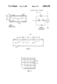
FIG. 1 is a cross-sectional view of a prior art Schottky barrier rectifier construction;
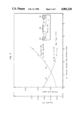
FIG. 2 is a schematic of a prior art Baker clamp circuit for reducing storage time;
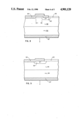
FIG. 3 is a cross-sectional view of the monolithic construction of a Schottky barrier in a bipolar junction according to the present invention;
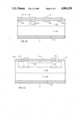
FIG. 4 is a top view of the structure of FIG. 3;
FIG. 5 is a plot representing the reverse recovery time as a function of forward voltage of several embodiments of the invention;
FIG. 6 is a cross-sectional view of an alternate embodiment of the invention as applied to the p-n junction of a high-voltage bipolar transistor; and
FIG. 7 is a plot representing the storage time and VCE (sat) as a function of base diffusion spacing;
FIG. 8 is a cross-sectional view of an alternate embodiment of the present invention having a Schottky barrier contact separated from the second p-n junction less than three (3) minority carrier diffusion lengths;
FIG. 9 is a cross-sectional view of a third alternate embodiment of the present invention having a Schottky barrier contact overlaying a portion of said p-n junction;
FIG. 10 is a cross-sectional view of a fourth alternate embodiment of the present invention having a plurality of isolated p+ diffusion regions in common with a common Schottky barrier contact; and
FIG. 11 is a cross-sectional view of a fifth alternate embodiment according to the present invention showing a relationship of the transverse dimensions of the p-n junction and the Schottky barrier contact within the range of 95:5.
DETAILED DESCRIPTION OF THE INVENTION
The construction of a conventional Schottky barrier device, Particularly a power rectifier, as formed by existing silicon photolithographic and diffusion techniques is exemplified in FIG. 1. The heavily-doped n-type donor material 10 has a lightly doped n-epitaxial layer 12. These semiconductor regions lie between an insulator layer 14, commonly formed from silicon dioxide, and an ohmic contact layer of conductive metal 18. The insulator layer 14 is sectioned to receive a Schottky barrier metal 16 which acts as a rectifying contact with the n-epitaxial layer 12. The abutment of the metal and the semiconductor creates a barrier effect at the rectifying contact. Majority carrier electrons from the n-epitaxial layer 12 pass easily into the metal 16, however, minority carrier flow is restricted. The structure thereby allows only a negligible storage of minority carriers at the barrier. Because the reverse recovery time (trr) of a semiconductor device is spent in the removal of minority carriers from the junction after the transition of an applied voltage from a forward-bias to reverse-bias state, a device having a Schottky barrier construction is capable of a low trr.
The method of achieving fast recovery performance without the use of recombination centers according to the invention is shown in FIG. 3. The p+ diffusions, distinguishable from conventional devices which are commonly integrated during the guard ring 15 of the FIG. 1 diffusion step, are distributed over the entire rectifier area. A continuous grid-like distribution of p+ material 22 thereby underlies the Schottky barrier metal 16 and each deposit 22 interrupts the surrounding n-type epitaxial layer 12. The distribution of deposits 22, each separated by a cell 28 having a Schottky barrier 24, forms a grid of alternating deposits 22 and Schottky barrier cells 28.
Viewed from above, as in FIG. 4, the arrangement of cells 28 within a grid 22 of p+ material appears as a lattice. The distribution of cell area per grid area is proportioned to achieve significant improvement in several parameters of device performance. During forward bias, carrier injection from the grid 22 achieves a low resistivity in the layer 12 due to conductivity modulation. During turn-off, the cell 28 acts as a recombination sink by aiding the removal of injected minority carriers during the recovery phase and thereby acts as a plane of recombination centers. Within the cell there is greatly reduced minority carrier storage.
The preferred embodiment has a cell-to-grid area ratio of approximately 1:1. However, the inclusion of even a relatively small grid area can reduce the typical forward voltage value for the common Schottky device. The number of cells are varied according to Table 1.
              TABLE I                                                     
______________________________________                                    
Relative Areas for Various Patterns with a                                
p+ Grid and Schottky Cells                                                
Pattern No.                                                               
           Cell Size  p+ Area  Schottky Area                              
______________________________________                                    
1          167    mils     5%    95%                                      
2          26     mils    17%    83%                                      
3          10     mils    33%    67%                                      
4          5      mils    50%    50%                                      
______________________________________                                    
The performance ratio of reverse recovery time per forward voltage for configurations of the invention may be seen in FIG. 5. A reduction in trr with a concurrent reduction in VF is indicated by a sequence of points 44 and 42 moving to the lower left corner of the graph representing the effect of a p+ grid with Schottky cells 44 or a Schottky grid with p+ cells 42. For comparison to the invention, FIG. 5 features the calculated best-performance curves for a conventional p-n junction device having an n-base layer thickness of either 12 micrometers or 45 micrometers in curves 46 and 48, respectively.
The trr to Vf ratios, if taken from typical gold- or platinum-doped rectifiers, would lie to the right of the best-performance curves 46 and 48. For example, data points 47A and 47B taken from two high-efficiency power rectifiers (UES 803 and UES 806) representative of the current art appear to the right of curves 46. The points 47A and 47B also reflect how common design practice compromises trr with low forward voltage, or vice versa.
The trr per VF data points in FIG. 5 are taken from the operation of several versions of diodes constructed according to the invention. The majority of the data points on curves 42 and 44 lie to the left of the conventional device best-Performance curves, thereby indicating that the invention achieves a major improvement over the typical trr per VF performance ratios of conventional devices. The positions of these data points also indicate no compromise in the achievement of low trr and VF values The two lower-leftmost data points represent the actual performance of the preferred embodiment, which utilizes a cell-to-grid area ratio of 1:1. In sum, none of the inventive embodiments use gold or platinum doping, yet they demonstrate superior performance without the problems attributable to recombination-center doping.
A method of incorporating the invention in a high-voltage transistor junction is shown in an alternate embodiment of FIG. 6. The p-type base region 62 is terminated to permit a Schottky barrier 24A between the base contact 50 and the n- collector layer 64. Diffused over the base layer 62 is an n+ layer 52 which underlies the emitter contact 54. An n+ layer 57 separates the collector contact 58 and the n-collector layer 64. The spacing between adjacent p layers 62 is small enough to eject a pinch-off of the depletion regions therein well before the onset of the collector-base junction voltage breakdown. By this "clamping" of the emitter to the collector, there will be little storage of minority carriers under the Schottky contact. Also, the Schottky contact will act as a recombination site for holes stored under the p-type base material 62.
As shown in FIG. 7, the device constructed according to the present invention has typical and typical VCE (sat ts characteristics 72 and 74 in FIG. 7. This figure shows that the storage time decreases monotonically with base diffusion spacing, D. The corresponding increase in VCE (sat) is still less than that found in the prior art, such as the Baker clamp of FIG. 2.
FIG. 8 shows a second alternate embodiment of the present invention which provides a bipolar junction structure including a p-n junction formed from a p+ diffusion region 82 and an n-type substrate 84 having an n epitaxial layer 86 and a metalized cathode terminal 87. A silicon oxide insulator or dielectric layer 83 is provided over the n epitaxial layer 86, and a separate silicon oxide layer 81 is provided over a portion of the p+ diffusion region 82. A metalization layer 85 is applied over the p+ diffusion region 82 and the silicon oxide insulation layer 81 of less than three (3) minority carrier diffusion lengths in dimension Lx to provide a Schottky barrier according to the present invention.
A third alternative embodiment of the present invention is shown in FIG. 9, which provides a bipolar junction structure including a p-n junction formed from a p+ diffusion region 92 in an n-type substrate 94 having an n epitaxial layer 96 and a metalized cathode terminal 97. A Schottky barrier junction is formed by a metalization layer 95 overlying a portion of the p+ diffusion region, including the p+ junction with the n epitaxial layer 96. An insulating layer 93, comprising a silicon oxide or other dielectric material is provided over a portion of the p+ diffusion region and the remaining of the n epitaxial layer 96.
A fourth alternative embodiment according to the present invention is shown in FIG. 10, which provides a bipolar junction structure including a p-n junction formed from a plurality of isolated p+ diffusion regions 102, 104, 106, and 108 in an n-type epitaxial layer 112 having an n-type substrate 110 and a metalized cathode terminal 114. A Schottky barrier contact in contact with each of the plurality of isolated p+ diffusion regions 102, 104, 106, and 108 is provided by a metalization layer 116 which overlies at least a portion of the p+ diffusion regions and the n epitaxial layer 112. This embodiment of the present invention envisions a spacing Ls between the p+ diffusion regions of less than three (3) minority carrier diffusion lengths, and a width Lp of the p+ diffusion regions of less than three (3) minority carrier diffusion lengths. Furthermore, the proportion of the spacing between the diffusion regions and the widths of the diffusion regions may be varied over a wide ratio including 5:95 to 95:5.
A fifth alternate embodiment of the present invention provides a bipolar junction structure including a p-n junction formed from a p+ diffusion region 122 of dimension Lp in an n-type substrate 124 having an n type epitaxial layer 126 and a metalized cathode terminal 128. A silicon oxide insulator or dielectric material 123 of dimension Lx is disposed about the periphery of the p+ diffusion region in contact with the n epitaxial layer 126. A metalization layer 125 overlays the p+ diffusion region, the silicon oxide insulating layer 123, forming Schottky barrier junction on the n epitaxial layer 126 at regions 127 having a dimension Ls. The remaining outward separated portion of the n epitaxial layer 126 is covered with a silicon oxide insulator or dielectric material 129. The preferred smallest transverse dimension Lx of the insulative layer 123 is less than three (3) minority carrier diffusion lengths, while the ratio of the width of the p+ diffusion region 122 to the width of the Schottky barrier region 127 (Lp:Ls) is preferrably less than 95:5.
Alternate embodiments, substitutions and engineering changes made by one skilled in the art are considered to be within the scope of the present invention, which is not to be limited except by the claims which follow.

Claims (9)

What is claimed is:
1. A rectifying semiconductor device providing increased minority carrier recombination during the recovery phase of the operation of said device, comprising:
a p-N junction formed from a P+ diffusion region having a grid-like pattern in an N-type substrate; and
a metalization layer in contact with said P+ diffusion region and said substrate, forming an array of Schottky barrier rectifying contact cells, wherein each of said cells is bounded by said P+ diffusion region.
2. The rectifying semiconductor device of claim I wherein the area of said P+ diffusion region is substantially equal to the aggregate cell area.
3. A rectifying semiconductor device providing increased minority carrier recombination during the recovery phase of the operation of said device, including:
a plurality of P-N junctions formed from a plurality of non-contiguous P+ diffusion regions in an N-type substrate; and
a metalization layer in contact with each of said non-contiguous P+ diffusion regions, and in contact with said N-type substrate, to form a continuous Schottky barrier contact with other than said P+ diffusion regions.
4. The rectifying semiconductor device of claim 3 wherein the distance between each nearest neighboring pair of said P-N junctions is less than three (30 minority carrier diffusion lengths.
5. The rectifying semiconductor device of claim 4 wherein the ratio of the width of the P+ diffusion region to the Schottky barrier therebetween is in the range of 95:5 to 5:95.
6. A rectifying semiconductor device providing increased minority carrier recombination during the recovery phase of the operation of said device, comprising:
a P-N junction formed from a P+ diffusion region in an N-type substrate;
a metalization layer in contact with said P+ diffusion region and said N-type substrate to form a Schottky barrier contact; and
an insulating region disposed about the periphery of the P+ diffusion region and in contact with said P+ diffusion region and said N-type substrate;
wherein said Schottky barrier contact is disposed within three minority carrier diffusion lengths of said P-N junction, and wherein the ratio of the width of said P+ diffusion region to the width of said Schottky barrier contact is no greater than 95:5.
7. The rectifying semiconductor device of claim 1, wherein said P+ diffusion region has a surface that is substantially coplanar with a surface of said N-type substrate, said metalization layer contacting said coplanar surfaces.
8. The rectifying semiconductor device of claim 3 wherein the distance between a nearest neighboring pair of said P-N junctions is less than three (3) minority carrier diffusion lengths.
9. The rectifying semiconductor device of claim 3 further comprising an insulating region disposed about the periphery of each of said P+ diffusion regions and in contact with the P+ diffusion region and said N-type substrate.
US07/061,189 1987-06-10 1987-06-10 Structure for fast-recovery bipolar devices Expired - Fee Related US4901120A (en)

Priority Applications (1)

Application Number Priority Date Filing Date Title
US07/061,189 US4901120A (en) 1987-06-10 1987-06-10 Structure for fast-recovery bipolar devices

Applications Claiming Priority (1)

Application Number Priority Date Filing Date Title
US07/061,189 US4901120A (en) 1987-06-10 1987-06-10 Structure for fast-recovery bipolar devices

Publications (1)

Publication Number Publication Date
US4901120A true US4901120A (en) 1990-02-13

Family

ID=22034210

Family Applications (1)

Application Number Title Priority Date Filing Date
US07/061,189 Expired - Fee Related US4901120A (en) 1987-06-10 1987-06-10 Structure for fast-recovery bipolar devices

Country Status (1)

Country Link
US (1) US4901120A (en)

Cited By (16)

* Cited by examiner, † Cited by third party
Publication number Priority date Publication date Assignee Title
US5184198A (en) * 1990-08-15 1993-02-02 Solid State Devices, Inc. Special geometry Schottky diode
US5859465A (en) * 1996-10-15 1999-01-12 International Rectifier Corporation High voltage power schottky with aluminum barrier metal spaced from first diffused ring
EP1119055A1 (en) * 2000-01-19 2001-07-25 Fabtech, Inc. Distributed reverse surge guard
US6396084B1 (en) 1998-08-31 2002-05-28 Fairchild Korea Semiconductor Ltd Structure of semiconductor rectifier
US6462393B2 (en) 2001-03-20 2002-10-08 Fabtech, Inc. Schottky device
US6573128B1 (en) * 2000-11-28 2003-06-03 Cree, Inc. Epitaxial edge termination for silicon carbide Schottky devices and methods of fabricating silicon carbide devices incorporating same
US6717229B2 (en) 2000-01-19 2004-04-06 Fabtech, Inc. Distributed reverse surge guard
US20040077305A1 (en) * 2001-04-02 2004-04-22 International Rectifier Corporation Process for forming fast recovery diode with a single large area P/N junction
US20040135153A1 (en) * 2003-01-15 2004-07-15 Sei-Hyung Ryu Multiple floating guard ring edge termination for silicon carbide devices and methods of fabricating silicon carbide devices incorporating same
US20060006394A1 (en) * 2004-05-28 2006-01-12 Caracal, Inc. Silicon carbide Schottky diodes and fabrication method
US20060118792A1 (en) * 2003-01-15 2006-06-08 Sei-Hyung Ryu Edge termination structures for silicon carbide devices and methods of fabricating silicon carbide devices incorporating same
DE10232425B4 (en) * 2001-08-22 2007-03-29 Mitsubishi Denki K.K. Semiconductor element
US20070215873A1 (en) * 2004-10-12 2007-09-20 Guy Silver Near natural breakdown device
DE10203820B4 (en) * 2001-01-31 2008-07-10 Fuji Electric Co., Ltd., Kawasaki Semiconductor component and method for its production
US7649496B1 (en) 2004-10-12 2010-01-19 Guy Silver EM rectifying antenna suitable for use in conjunction with a natural breakdown device
US8901699B2 (en) 2005-05-11 2014-12-02 Cree, Inc. Silicon carbide junction barrier Schottky diodes with suppressed minority carrier injection

Citations (6)

* Cited by examiner, † Cited by third party
Publication number Priority date Publication date Assignee Title
US4253105A (en) * 1980-07-03 1981-02-24 Rca Corporation Semiconductor power device incorporating a schottky barrier diode between base and emitter of a PNP device
US4370670A (en) * 1979-04-11 1983-01-25 Fujitsu Limited Transistor with plural parallel units
US4405934A (en) * 1981-04-13 1983-09-20 Texas Instruments Incorporated NPM Anti-saturation clamp for NPN logic gate transistor
US4536945A (en) * 1983-11-02 1985-08-27 National Semiconductor Corporation Process for producing CMOS structures with Schottky bipolar transistors
US4641174A (en) * 1983-08-08 1987-02-03 General Electric Company Pinch rectifier
US4691223A (en) * 1984-11-09 1987-09-01 Hitachi, Ltd. Semiconductor device having high breakdown voltage

Patent Citations (6)

* Cited by examiner, † Cited by third party
Publication number Priority date Publication date Assignee Title
US4370670A (en) * 1979-04-11 1983-01-25 Fujitsu Limited Transistor with plural parallel units
US4253105A (en) * 1980-07-03 1981-02-24 Rca Corporation Semiconductor power device incorporating a schottky barrier diode between base and emitter of a PNP device
US4405934A (en) * 1981-04-13 1983-09-20 Texas Instruments Incorporated NPM Anti-saturation clamp for NPN logic gate transistor
US4641174A (en) * 1983-08-08 1987-02-03 General Electric Company Pinch rectifier
US4536945A (en) * 1983-11-02 1985-08-27 National Semiconductor Corporation Process for producing CMOS structures with Schottky bipolar transistors
US4691223A (en) * 1984-11-09 1987-09-01 Hitachi, Ltd. Semiconductor device having high breakdown voltage

Non-Patent Citations (12)

* Cited by examiner, † Cited by third party
Title
Amemiya et al., "Novel Low-Loss and High-Speed Diode Utilizing an `Ideal` Ohmic Contact," IEEE Transactions on Electron Devices, vol. ED-29, No. 2, Feb. 1982, pp. 236-243.
Amemiya et al., Novel Low Loss and High Speed Diode Utilizing an Ideal Ohmic Contact, IEEE Transactions on Electron Devices, vol. ED 29, No. 2, Feb. 1982, pp. 236 243. *
Baliga, "The Pinch Rectifier: A Low-Forward-Drop High-Speed Power Diode," IEEE Electron Device Letters, vol. EDL-5, No. 6, Jun. 1984, pp. 194-196.
Baliga, The Pinch Rectifier: A Low Forward Drop High Speed Power Diode, IEEE Electron Device Letters, vol. EDL 5, No. 6, Jun. 1984, pp. 194 196. *
Brill et al., "Power Transistor with Reduced Minority Carrier Storage," IBM Technical Disclosure Bulletin, vol. 19, No. 10, Mar. 1977, pp. 3787-3788.
Brill et al., Power Transistor with Reduced Minority Carrier Storage, IBM Technical Disclosure Bulletin, vol. 19, No. 10, Mar. 1977, pp. 3787 3788. *
Hower et al., "Schottky Rectifiers for Low-Voltage Outputs," APEC Meeting, New Orleans, Apr. 1986, Unitrode Corp., Watertown, MA., pp. 1-10.
Hower et al., Schottky Rectifiers for Low Voltage Outputs, APEC Meeting, New Orleans, Apr. 1986, Unitrode Corp., Watertown, MA., pp. 1 10. *
Shimizu et al., "High-Speed Low-Loss p-n Diode Having a Channel Structure," IEEE Transactions on Electron Devices, vol. ED-31, No. 9, Sep. 1984, pp. 1314-1319.
Shimizu et al., High Speed Low Loss p n Diode Having a Channel Structure, IEEE Transactions on Electron Devices, vol. ED 31, No. 9, Sep. 1984, pp. 1314 1319. *
Zeidenbergs, IBM Technical Disclosure Bulletin, vol. 14, No. 4, Sep. 1971, p. 1104, "Multiemitter Schottky Barrier Transistor with Negligible Emitter-to-Emitter Gain".
Zeidenbergs, IBM Technical Disclosure Bulletin, vol. 14, No. 4, Sep. 1971, p. 1104, Multiemitter Schottky Barrier Transistor with Negligible Emitter to Emitter Gain . *

Cited By (28)

* Cited by examiner, † Cited by third party
Publication number Priority date Publication date Assignee Title
US5184198A (en) * 1990-08-15 1993-02-02 Solid State Devices, Inc. Special geometry Schottky diode
US5859465A (en) * 1996-10-15 1999-01-12 International Rectifier Corporation High voltage power schottky with aluminum barrier metal spaced from first diffused ring
US6396084B1 (en) 1998-08-31 2002-05-28 Fairchild Korea Semiconductor Ltd Structure of semiconductor rectifier
US6717229B2 (en) 2000-01-19 2004-04-06 Fabtech, Inc. Distributed reverse surge guard
EP1119055A1 (en) * 2000-01-19 2001-07-25 Fabtech, Inc. Distributed reverse surge guard
US6673662B2 (en) 2000-11-28 2004-01-06 Cree, Inc. Epitaxial edge termination for silicon carbide Schottky devices and methods of fabricating silicon carbide devices incorporating same
US6573128B1 (en) * 2000-11-28 2003-06-03 Cree, Inc. Epitaxial edge termination for silicon carbide Schottky devices and methods of fabricating silicon carbide devices incorporating same
DE10203820B4 (en) * 2001-01-31 2008-07-10 Fuji Electric Co., Ltd., Kawasaki Semiconductor component and method for its production
US6710419B2 (en) 2001-03-20 2004-03-23 Fabtech, Inc. Method of manufacturing a schottky device
US6462393B2 (en) 2001-03-20 2002-10-08 Fabtech, Inc. Schottky device
US7091572B2 (en) 2001-04-02 2006-08-15 International Rectifier Corporation Fast recovery diode with a single large area p/n junction
US20040077305A1 (en) * 2001-04-02 2004-04-22 International Rectifier Corporation Process for forming fast recovery diode with a single large area P/N junction
US6927141B2 (en) 2001-04-02 2005-08-09 International Rectifier Corporation Process for forming fast recovery diode with a single large area P/N junction
US20060017130A1 (en) * 2001-04-02 2006-01-26 International Rectifier Corporation Fast recovery diode with a single large area P/N junction
DE10232425B4 (en) * 2001-08-22 2007-03-29 Mitsubishi Denki K.K. Semiconductor element
US7026650B2 (en) 2003-01-15 2006-04-11 Cree, Inc. Multiple floating guard ring edge termination for silicon carbide devices
US20060118792A1 (en) * 2003-01-15 2006-06-08 Sei-Hyung Ryu Edge termination structures for silicon carbide devices and methods of fabricating silicon carbide devices incorporating same
US20040135153A1 (en) * 2003-01-15 2004-07-15 Sei-Hyung Ryu Multiple floating guard ring edge termination for silicon carbide devices and methods of fabricating silicon carbide devices incorporating same
US7419877B2 (en) 2003-01-15 2008-09-02 Cree, Inc. Methods of fabricating silicon carbide devices including multiple floating guard ring edge termination
US20090035926A1 (en) * 2003-01-15 2009-02-05 Sei-Hyung Ryu Methods of Fabricating Silicon Carbide Devices Incorporating Multiple Floating Guard Ring Edge Terminations
US7842549B2 (en) 2003-01-15 2010-11-30 Cree, Inc. Methods of fabricating silicon carbide devices incorporating multiple floating guard ring edge terminations
US20110081772A1 (en) * 2003-01-15 2011-04-07 Sei Hyung Ryu Methods of fabricating silicon carbide devices incorporating multiple floating guard ring edge terminations
US8124480B2 (en) 2003-01-15 2012-02-28 Cree, Inc. Methods of fabricating silicon carbide devices incorporating multiple floating guard ring edge terminations
US9515135B2 (en) 2003-01-15 2016-12-06 Cree, Inc. Edge termination structures for silicon carbide devices
US20060006394A1 (en) * 2004-05-28 2006-01-12 Caracal, Inc. Silicon carbide Schottky diodes and fabrication method
US20070215873A1 (en) * 2004-10-12 2007-09-20 Guy Silver Near natural breakdown device
US7649496B1 (en) 2004-10-12 2010-01-19 Guy Silver EM rectifying antenna suitable for use in conjunction with a natural breakdown device
US8901699B2 (en) 2005-05-11 2014-12-02 Cree, Inc. Silicon carbide junction barrier Schottky diodes with suppressed minority carrier injection

Similar Documents

Publication Publication Date Title
US7276771B2 (en) Diode and method for manufacturing the same
US4862229A (en) Semiconductor Schottky devices having improved voltage blocking characteristics
US4901120A (en) Structure for fast-recovery bipolar devices
EP0009367B1 (en) Gate turn-off thyristor
US5063428A (en) Semiconductor element having a p-zone on the anode side and an adjacent, weakly doped n-base zone
US4607270A (en) Schottky barrier diode with guard ring
EP0345435B2 (en) Semiconductor device with a high breakdown voltage and method for its manufacture
JPH037149B2 (en)
US6011279A (en) Silicon carbide field controlled bipolar switch
EP0646964B1 (en) Integrated structure active clamp for the protection of power devices against overvoltages, and manufacturing process thereof
US10056501B2 (en) Power diode with improved reverse-recovery immunity
KR100397882B1 (en) Field effect controllable semiconductor component
US5432360A (en) Semiconductor device including an anode layer having low density regions by selective diffusion
EP0103138A2 (en) Semiconductor rectifier diode
JP3352160B2 (en) Solid suppressor
US20020000565A1 (en) Surface breakdown bidirectional breakover protection component
JP3072753B2 (en) Semiconductor device and manufacturing method
JPH06283727A (en) Power semiconductor element
US4727408A (en) Semiconductor device with high breakdown voltage vertical transistor and fabricating method therefor
CN114400255A (en) Planar power MOSFET device integrated with junction barrier Schottky diode
JP2622521B2 (en) Gate cut-off thyristor and manufacturing method thereof
EP0157207A2 (en) Gate turn-off thyristor
JPH05136015A (en) Semiconductor device
US7053404B2 (en) Active semiconductor component with an optimized surface area
WO2000035018A1 (en) Sidewall junction for bipolar semiconductor devices

Legal Events

Date Code Title Description
AS Assignment

Owner name: UNITRODE CORPORATION, 5 FORBES RD., LEXINGTON, MA

Free format text: ASSIGNMENT OF ASSIGNORS INTEREST.;ASSIGNORS:WEAVER, CARSON E.;HOWER, PHILIP L.;REEL/FRAME:004727/0570

Effective date: 19870603

Owner name: UNITRODE CORPORATION, A CORP. OF MD,MASSACHUSETTS

Free format text: ASSIGNMENT OF ASSIGNORS INTEREST;ASSIGNORS:WEAVER, CARSON E.;HOWER, PHILIP L.;REEL/FRAME:004727/0570

Effective date: 19870603

CC Certificate of correction
AS Assignment

Owner name: MICRO USPD, INC., MASSACHUSETTS

Free format text: ASSIGNMENT OF ASSIGNORS INTEREST;ASSIGNOR:UNITRODE CORPORATION;REEL/FRAME:006608/0819

Effective date: 19920702

REMI Maintenance fee reminder mailed
LAPS Lapse for failure to pay maintenance fees
FP Lapsed due to failure to pay maintenance fee

Effective date: 19940213

STCH Information on status: patent discontinuation

Free format text: PATENT EXPIRED DUE TO NONPAYMENT OF MAINTENANCE FEES UNDER 37 CFR 1.362