US4901051A - Platinum temperature sensor - Google Patents
Platinum temperature sensor Download PDFInfo
- Publication number
- US4901051A US4901051A US07/239,195 US23919588A US4901051A US 4901051 A US4901051 A US 4901051A US 23919588 A US23919588 A US 23919588A US 4901051 A US4901051 A US 4901051A
- Authority
- US
- United States
- Prior art keywords
- platinum
- platinum resistance
- outermost
- holes
- temperature sensor
- Prior art date
- Legal status (The legal status is an assumption and is not a legal conclusion. Google has not performed a legal analysis and makes no representation as to the accuracy of the status listed.)
- Expired - Lifetime
Links
Images

Classifications
-
- H—ELECTRICITY
- H01—ELECTRIC ELEMENTS
- H01C—RESISTORS
- H01C7/00—Non-adjustable resistors formed as one or more layers or coatings; Non-adjustable resistors made from powdered conducting material or powdered semi-conducting material with or without insulating material
- H01C7/02—Non-adjustable resistors formed as one or more layers or coatings; Non-adjustable resistors made from powdered conducting material or powdered semi-conducting material with or without insulating material having positive temperature coefficient
- H01C7/021—Non-adjustable resistors formed as one or more layers or coatings; Non-adjustable resistors made from powdered conducting material or powdered semi-conducting material with or without insulating material having positive temperature coefficient formed as one or more layers or coatings
-
- G—PHYSICS
- G01—MEASURING; TESTING
- G01K—MEASURING TEMPERATURE; MEASURING QUANTITY OF HEAT; THERMALLY-SENSITIVE ELEMENTS NOT OTHERWISE PROVIDED FOR
- G01K7/00—Measuring temperature based on the use of electric or magnetic elements directly sensitive to heat ; Power supply therefor, e.g. using thermoelectric elements
- G01K7/16—Measuring temperature based on the use of electric or magnetic elements directly sensitive to heat ; Power supply therefor, e.g. using thermoelectric elements using resistive elements
- G01K7/18—Measuring temperature based on the use of electric or magnetic elements directly sensitive to heat ; Power supply therefor, e.g. using thermoelectric elements using resistive elements the element being a linear resistance, e.g. platinum resistance thermometer
-
- H—ELECTRICITY
- H01—ELECTRIC ELEMENTS
- H01C—RESISTORS
- H01C1/00—Details
- H01C1/14—Terminals or tapping points or electrodes specially adapted for resistors; Arrangements of terminals or tapping points or electrodes on resistors
- H01C1/1406—Terminals or electrodes formed on resistive elements having positive temperature coefficient
-
- Y—GENERAL TAGGING OF NEW TECHNOLOGICAL DEVELOPMENTS; GENERAL TAGGING OF CROSS-SECTIONAL TECHNOLOGIES SPANNING OVER SEVERAL SECTIONS OF THE IPC; TECHNICAL SUBJECTS COVERED BY FORMER USPC CROSS-REFERENCE ART COLLECTIONS [XRACs] AND DIGESTS
- Y10—TECHNICAL SUBJECTS COVERED BY FORMER USPC
- Y10T—TECHNICAL SUBJECTS COVERED BY FORMER US CLASSIFICATION
- Y10T29/00—Metal working
- Y10T29/49—Method of mechanical manufacture
- Y10T29/49002—Electrical device making
- Y10T29/49082—Resistor making
- Y10T29/49085—Thermally variable
Definitions
- the present invention relates to a platinum temperature sensor, and more particularly, it relates to a platinum temperature sensor employing a platinum resistance thermometer.
- Platinum being chemically stable and having high temperature dependency of electrical resistance, is applied as a material for a temperature sensor.
- a platinum temperature sensor a platinum wire is spirally wound on an insulator, or a platinum resistance pattern is formed as a thick or thin film on a single plate-type alumina substrate, as shown in U.S. Pat. Nos. 4,028,657, 4,050,052 or 3,781,749.
- the winding type platinum temperature sensor is high in cost and cannot be sufficiently reduced in size, and high resistance values cannot be attained.
- the size must be increased in order to attain a high resistance value, while a high resistance value cannot be attained if the size is reduced.
- U.S. Pat. No. 3,781,749 discloses a platinum temperature sensor which is obtained by stacking platinum patterns which are formed in a linear straight manner on each layer.
- this sensor has problems similar to those of the aforementioned conventional platinum temperature sensors since sufficient pattern length cannot be attained in each layer.
- An object of the present invention is to obtain a small-sized platinum temperature sensor having a high resistance value at a low cost.
- a platinum temperature sensor comprises a plurality of stacked plate-type ceramic sheets, platinum resistance patterns formed on the surfaces of respective ceramic sheets so that each of the platinum resistance patterns has a plurality of bent portions, and connecting means for connecting adjacent ones of the platinum resistance patterns with each other, the connecting means being provided between the ceramic sheets.
- the connecting means may be formed by through holes provided in the ceramic sheets, and metal paste members arranged in the through holes, which are continuous with both ends of the platinum resistance patterns.
- the platinum temperature sensor may further be provided with through holes on the outermost one of the ceramic sheets communicating with the bent portions of the platinum resistance pattern located under the outermost ceramic sheet.
- Resistance adjusting lines may be provided on the outer surface of the outermost ceramic sheet and connected to the platinum resistance pattern located under the outermost ceramic sheet through the through holes. Each such resistance adjusting line may adjust the resistance of the platinum resistance pattern, by conductively interconnecting the corresponding bent portions of the pattern to which it is connected; and such resistance adjusting lines may be cut, to eliminate such interconnecting of the bent portions.
- lead wires may be connected by means of electrode paste members to both ends of the platinum resistance patterns which are connected with each other by the connecting means.
- the platinum temperature sensor measures temperature as a function of linear variations in the electrical resistance of the platinum resistance patterns, which serve as temperature sensing elements, said variations being caused by temperature change.
- the platinum resistance patterns are formed on the surfaces of the plurality of stacked plate-type ceramic sheets. Adjacent ones of the platinum resistance patterns provided between the ceramic sheets are connected with each other by the connecting means.
- the platinum resistance patterns can be greater in length than in conventional platinum resistance patterns, so a high resistance value can be attained with a senser having a small size.
- the manufacturing cost is reduced since the temperature sensor is formed by stacking a plurality of ceramic sheets. According to the present invention, therefore, a platinum temperature sensor can be obtained with a lower cost, a smaller size and a higher resistance value, as compared with the conventional platinum temperature sensor.
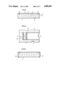
- FIG. 1 is a partially fragmented perspective view showing an embodiment of the present invention
- FIG. 2 is an exploded perspective view of the embodiment shown in FIG. 1;
- FIG. 3 is a sectional view taken along the line III--III in FIG. 1;
- FIG. 4 is a sectional view taken along the line IV--IV in FIG. 2;
- FIG. 5 is a sectional view corresponding to FIG. 3, showing another embodiment of the present invention.
- FIG. 1 is a partially fragmented perspective view showing an embodiment of the present invention.
- a platinum temperature sensor according to the present invention comprises a platinum temperature sensor body 1 and a pair of lead wires 2 and 3 extending from the platinum temperature sensor body 1.
- the platinum temperature sensor body 1 is formed of four plate-type ceramic sheets which are integrally fired after being stacked.
- FIG. 2 is a perspective view showing the embodiment of FIG. 1 in an exploded manner.
- the lowermost ceramic sheet 4 is provided on its upper surface with a platinum resistance pattern 5 which is formed in a zigzag manner.
- a first end portion of the platinum resistance pattern 5 is linearly extended from the zigzag portion, and said first end portion is connected to an electrode 6 which is formed in a portion at a peripheral edge of the ceramic sheet 4.
- a ceramic sheet 7 provided on the ceramic sheet 4 also has a zigzag platinum resistance pattern 8 on its upper surface.
- a first end of the platinum resistance pattern 8 is vertically aligned with the second end of the platinum resistance pattern 5.
- the ceramic sheet 7 is provided with a perpendicular through hole 9 at the first end portion of the platinum resistance pattern 8, which is aligned with the second end of the platinum resistance pattern 5.
- a ceramic sheet 10 provided on the ceramic sheet 7 also has a zigzag platinum resistance pattern 11.
- the ceramic sheet 10 has a perpendicular through hole 12 at a first end portion of the platinum resistance pattern 11, which is aligned with the second end of the platinum resistance pattern 8, the latter being provided with no through hole.
- the second end of the platinum resistance pattern 11 is connected to an electrode 13 which is formed at a peripheral edge of the ceramic sheet 10.
- a ceramic sheet 14 provided on the ceramic sheet 10 has a large number of through holes 15, which are formed slightly inside peripheral edges of the ceramic sheet 14 in positions of the zigzag pattern corresponding to bent portions of the platinum resistance pattern 11 provided under the same.
- the lead wires 2 and 3 are respectively connected to the electrodes 13 and 6 by silver baking. As shown in FIG. 1, some of the through holes 15 are connected with each other by resistance adjusting lines 16 which are applied/fired onto the upper surface of the ceramic sheet 14 in positions corresponding to bent portions of the platinum resistance pattern 11.
- the resistance adjusting lines 16 are adapted to electrically connect the bent portions of the platinum resistance pattern 11 with each other through the through holes 15.
- a ceramic slurry layer 17 is further applied onto the upper surface of the ceramic sheet 14, as shown in FIG. 1.
- the ceramic slurry layer 17 is adapted to fill up those of the through holes 15 which are not provided with the resistance adjusting lines 16, as shown in FIG. 3.
- the platinum resistance pattern 11 and the resistance adjusting lines 16 are prevented from outward exposure.
- a connecting line 18 of silver paste is provided in the through hole 12.
- the lower end of the connecting line 18 is electrically connected to the second end of the platinum resistance pattern 8 while the upper end thereof is connected to the first end of the platinum resistance pattern 11, thereby electrically connecting the platinum resistance patterns 8 and 11 with each other.
- the through hole 9 (see FIG. 2) is structured similarly to the through hole 12, thereby to electrically connect the platinum resistance patterns 5 and 8 with each other.
- the platinum temperature sensor can be disposed in a circuit for carring out temperature measurement by the Wheatstone bridge method or the constant current process, for example.
- the platinum resistance patterns 5, 8 and 11 serve as temperature sensing elements whose electrical resistance changes linearly with temperature, thereby measuring the temperature of the object.
- the resistance of the platinum resistance patterns 5, 8 and 11 is adjusted by selectively cutting the resistance adjusting lines 16 prior to application of the ceramic slurry layer 17. After such resistance adjustment, the ceramic slurry layer 17 is formed on the ceramic sheet 14 to cover the through holes 15 and the resistance adjusting lines 16, thereby improving resistance against the atmosphere and moisture.
- the platinum resistance patterns 5, 8 and 11 are provided on three of the ceramic green sheets, and the through holes 15 are formed in the remaining ceramic green sheet.
- the platinum resistance patterns 5, 8 and 11 may be provided in the form of thick films applied by silk screening, or in the form of thin films provided by evaporation, etc.
- the through holes 9 and 12 and the electrodes 6 and 13 shown in FIG. 2 are formed on the ceramic green sheets provided with the platinum resistance patterns 5, 8 and 11.
- the four ceramic green sheets thus obtained are stacked as shown in FIG. 2, and connected with each other under pressure. Then, the resistance adjusting lines 16 are so applied as to connect the through holes 15 corresponding to the bent portions of the platinum resistance pattern 11.
- the laminate thus obtained is cofired, thereby providing the platinum temperature sensor body 1.
- the lead wires 2 and 3 are connected to the electrodes 6 and 13 of the platinum temperature sensor body 1 by silver baking.
- the resistance of the platinum resistance patterns 5, 8 and 11 of the platinum temperature sensor body 1 is measured through the lead wires 2 and 3, and the resistance adjusting lines 16 may be cut to attain a prescribed resistance.
- the ceramic slurry layer 17 is applied onto the upper surface of the platinum temperature sensor body 1, to cover the through holes 15 and the resistance adjusting lines 16. Further, the entire body is fired to integrally fix the ceramic slurry layer 17 to the platinum temperature sensor body 1, thereby providing the platinum temperature sensor as shown in FIG. 1.
- the lead wires 2 and 3 may be replaced by outer electrodes 20 and 21 as shown in FIG. 5, by applying silver paste on side wall surfaces of the platinum temperature sensor body 1.
- the adjustment can be performed by coupling the through holes 15 appropriately by silver baking.
- the ceramic slurry layer 17 may be replaced by a glass coating layer.
- the means for connecting the platinum resistance patterns 5, 8 and 11 is not restricted to the through holes 9 and 12 and the connecting line 18.
- the platinum resistance patterns 5, 8 and 11 may be connected with each other by externally provided connecting lines.
- the patterns may arbitrarily be formed on two or more layers.
- the lead wires 2 and 3 may be connected when the laminate of the ceramic green sheets is cofired.
- the lead wires 2 and 3 are prepared from a material having a high melting point, to withstand the temperature for firing the laminate.
Abstract
Description
Claims (18)
Applications Claiming Priority (2)
| Application Number | Priority Date | Filing Date | Title |
|---|---|---|---|
| JP62222868A JP2564845B2 (en) | 1987-09-04 | 1987-09-04 | Platinum temperature sensor |
| JP62-222868 | 1987-09-04 |
Publications (1)
| Publication Number | Publication Date |
|---|---|
| US4901051A true US4901051A (en) | 1990-02-13 |
Family
ID=16789145
Family Applications (1)
| Application Number | Title | Priority Date | Filing Date |
|---|---|---|---|
| US07/239,195 Expired - Lifetime US4901051A (en) | 1987-09-04 | 1988-08-31 | Platinum temperature sensor |
Country Status (4)
| Country | Link |
|---|---|
| US (1) | US4901051A (en) |
| JP (1) | JP2564845B2 (en) |
| DE (1) | DE3829764C2 (en) |
| GB (1) | GB2211027B (en) |
Cited By (27)
| Publication number | Priority date | Publication date | Assignee | Title |
|---|---|---|---|---|
| US5109183A (en) * | 1990-12-13 | 1992-04-28 | U.S. Philips Corporation | High pressure discharge lamp having a simplified mount construction |
| US5159242A (en) * | 1990-12-12 | 1992-10-27 | North American Philips Corporation | High pressure discharge lamp having an integral thick film resistor with multiple resistive elements |
| US5199791A (en) * | 1990-06-11 | 1993-04-06 | Murata Manufacturing Co., Ltd. | Temperature sensor |
| US5242225A (en) * | 1990-06-11 | 1993-09-07 | Murata Manufacturing Co., Ltd. | Temperature sensor |
| US5327046A (en) * | 1990-12-12 | 1994-07-05 | North American Philips Corporation | High pressure discharge lamp having overcurrent fuse protection |
| US5331134A (en) * | 1992-05-21 | 1994-07-19 | Shin-Etsu Chemical Co., Ltd. | Double-layered ceramic heater |
| US5406246A (en) * | 1990-08-14 | 1995-04-11 | Robert Bosch Gmbh | Temperature sensor and method for producing temperature sensor elements |
| US5539186A (en) * | 1992-12-09 | 1996-07-23 | International Business Machines Corporation | Temperature controlled multi-layer module |
| US5573692A (en) * | 1991-03-11 | 1996-11-12 | Philip Morris Incorporated | Platinum heater for electrical smoking article having ohmic contact |
| US5823680A (en) * | 1993-12-27 | 1998-10-20 | Ngk Insulators, Ltd. | Temperature sensor |
| EP0939410A2 (en) * | 1998-02-26 | 1999-09-01 | Abb Research Ltd. | Thermistor manufacturing process and application of thermistor as current limiter |
| US20030098771A1 (en) * | 1998-12-07 | 2003-05-29 | Aravind Padmanabhan | Robust fluid and property microsensor assembly made of optimal material |
| US6642835B2 (en) * | 1998-11-11 | 2003-11-04 | Robert Bosch Gmbh | Ceramic layer system and method for producing a ceramic heating device |
| US6653926B1 (en) * | 1999-01-14 | 2003-11-25 | Sensotherm Temperatursensorik Gmbh | Platinum temperature sensor and its method of production |
| WO2005098382A1 (en) * | 2004-04-05 | 2005-10-20 | E.G.O. Elektro-Gerätebau GmbH | Temperature sensor and method for adjusting said type of temperature sensor |
| US20100034237A1 (en) * | 2008-08-07 | 2010-02-11 | Melexis Nv Microelectronic Integrated Systems | Laminated temperature sensor |
| US20100108661A1 (en) * | 2008-10-31 | 2010-05-06 | United Technologies Corporation | Multi-layer heating assembly and method |
| US20100150204A1 (en) * | 2007-05-18 | 2010-06-17 | Yamatake Corporation | Process for manufacturing platinum resistance thermometer |
| US20100150205A1 (en) * | 2008-12-15 | 2010-06-17 | Delphi Technologies, Inc. | Combined sensor |
| US20110134961A1 (en) * | 2006-07-21 | 2011-06-09 | Georg Bernitz | Temperature Measuring Sensor and Method of Producing Same |
| WO2014045000A1 (en) * | 2012-09-20 | 2014-03-27 | University Of Southampton | Apparatus with a sensor having strain compensation means for sensing at least one parameter in water the |
| EP3136067A4 (en) * | 2014-04-21 | 2017-11-22 | Kyocera Corporation | Wiring substrate and temperature sensing element |
| DK179268B1 (en) * | 2011-06-01 | 2018-03-19 | Heraeus Sensor Technology Gmbh | Mass production of small temperature sensors with flip chips |
| US20180180489A1 (en) * | 2015-12-24 | 2018-06-28 | Moda-Innochips Co., Ltd. | Temperature sensor |
| US11114223B1 (en) * | 2020-07-27 | 2021-09-07 | Tronics MEMS, Inc. | Three-dimensional thermistor platform and a method for manufacturing the same |
| US11131586B2 (en) * | 2017-05-16 | 2021-09-28 | Koa Corporation | Temperature sensor element |
| US11226240B2 (en) * | 2017-04-26 | 2022-01-18 | Kyocera Corporation | Temperature sensor and temperature measuring device |
Families Citing this family (5)
| Publication number | Priority date | Publication date | Assignee | Title |
|---|---|---|---|---|
| JP2968111B2 (en) * | 1991-11-22 | 1999-10-25 | 日本特殊陶業株式会社 | Resistor physical quantity sensor with migration prevention pattern |
| JP3203803B2 (en) * | 1992-09-01 | 2001-08-27 | 株式会社デンソー | Thermistor type temperature sensor |
| DE19803506A1 (en) * | 1998-01-30 | 1999-08-05 | Ego Elektro Geraetebau Gmbh | Method of manufacturing an electrical sensor and electrical sensor |
| KR101891279B1 (en) * | 2016-11-30 | 2018-09-28 | 주식회사 유라테크 | Stacked-type temperature sensor suitable for high temperature |
| JP6567700B2 (en) * | 2018-01-04 | 2019-08-28 | Koa株式会社 | Temperature sensor element |
Citations (4)
| Publication number | Priority date | Publication date | Assignee | Title |
|---|---|---|---|---|
| US3781749A (en) * | 1971-11-18 | 1973-12-25 | Johnson Matthey Co Ltd | Resistance thermometer element |
| US3845443A (en) * | 1972-06-14 | 1974-10-29 | Bailey Meter Co | Thin film resistance thermometer |
| US4028657A (en) * | 1974-10-24 | 1977-06-07 | W. C. Heraeus Gmbh | Deposited layer type thermometric resistance structure |
| US4050052A (en) * | 1975-06-21 | 1977-09-20 | W. C. Heraeus Gmbh | Electrical temperature measuring resistor structure, particularly for resistance thermometers |
Family Cites Families (3)
| Publication number | Priority date | Publication date | Assignee | Title |
|---|---|---|---|---|
| US3575053A (en) * | 1968-07-11 | 1971-04-13 | Mc Donnell Douglas Corp | Cryogenic linear temperature sensor |
| DE2048489A1 (en) * | 1969-10-03 | 1971-04-15 | Vyzk Ustav Organickysch Syntez | Temperature surface sensor |
| US4146957A (en) * | 1977-01-17 | 1979-04-03 | Engelhard Minerals & Chemicals Corporation | Thick film resistance thermometer |
-
1987
- 1987-09-04 JP JP62222868A patent/JP2564845B2/en not_active Expired - Lifetime
-
1988
- 1988-08-31 US US07/239,195 patent/US4901051A/en not_active Expired - Lifetime
- 1988-09-01 DE DE3829764A patent/DE3829764C2/en not_active Expired - Lifetime
- 1988-09-02 GB GB8820797A patent/GB2211027B/en not_active Expired - Lifetime
Patent Citations (4)
| Publication number | Priority date | Publication date | Assignee | Title |
|---|---|---|---|---|
| US3781749A (en) * | 1971-11-18 | 1973-12-25 | Johnson Matthey Co Ltd | Resistance thermometer element |
| US3845443A (en) * | 1972-06-14 | 1974-10-29 | Bailey Meter Co | Thin film resistance thermometer |
| US4028657A (en) * | 1974-10-24 | 1977-06-07 | W. C. Heraeus Gmbh | Deposited layer type thermometric resistance structure |
| US4050052A (en) * | 1975-06-21 | 1977-09-20 | W. C. Heraeus Gmbh | Electrical temperature measuring resistor structure, particularly for resistance thermometers |
Cited By (36)
| Publication number | Priority date | Publication date | Assignee | Title |
|---|---|---|---|---|
| US5199791A (en) * | 1990-06-11 | 1993-04-06 | Murata Manufacturing Co., Ltd. | Temperature sensor |
| US5242225A (en) * | 1990-06-11 | 1993-09-07 | Murata Manufacturing Co., Ltd. | Temperature sensor |
| US5406246A (en) * | 1990-08-14 | 1995-04-11 | Robert Bosch Gmbh | Temperature sensor and method for producing temperature sensor elements |
| US5159242A (en) * | 1990-12-12 | 1992-10-27 | North American Philips Corporation | High pressure discharge lamp having an integral thick film resistor with multiple resistive elements |
| US5327046A (en) * | 1990-12-12 | 1994-07-05 | North American Philips Corporation | High pressure discharge lamp having overcurrent fuse protection |
| US5109183A (en) * | 1990-12-13 | 1992-04-28 | U.S. Philips Corporation | High pressure discharge lamp having a simplified mount construction |
| US5573692A (en) * | 1991-03-11 | 1996-11-12 | Philip Morris Incorporated | Platinum heater for electrical smoking article having ohmic contact |
| US5331134A (en) * | 1992-05-21 | 1994-07-19 | Shin-Etsu Chemical Co., Ltd. | Double-layered ceramic heater |
| US5539186A (en) * | 1992-12-09 | 1996-07-23 | International Business Machines Corporation | Temperature controlled multi-layer module |
| US5823680A (en) * | 1993-12-27 | 1998-10-20 | Ngk Insulators, Ltd. | Temperature sensor |
| EP0939410A2 (en) * | 1998-02-26 | 1999-09-01 | Abb Research Ltd. | Thermistor manufacturing process and application of thermistor as current limiter |
| EP0939410A3 (en) * | 1998-02-26 | 2000-07-26 | DaimlerChrysler AG | Thermistor manufacturing process and application of thermistor as current limiter |
| US6642835B2 (en) * | 1998-11-11 | 2003-11-04 | Robert Bosch Gmbh | Ceramic layer system and method for producing a ceramic heating device |
| US20030098771A1 (en) * | 1998-12-07 | 2003-05-29 | Aravind Padmanabhan | Robust fluid and property microsensor assembly made of optimal material |
| US7233226B2 (en) | 1999-01-14 | 2007-06-19 | Sensotherm Temperatursenorik Gmbh | Method of producing a platinum temperature sensor |
| US20060132281A1 (en) * | 1999-01-14 | 2006-06-22 | Sensotherm Temperatursensorik, Gmbh | Method of producing a platinum temperature sensor |
| US6653926B1 (en) * | 1999-01-14 | 2003-11-25 | Sensotherm Temperatursensorik Gmbh | Platinum temperature sensor and its method of production |
| US20040070487A1 (en) * | 1999-01-14 | 2004-04-15 | Sensotherm Temperatursensorik, Gmbh | Platinum temperature sensor |
| WO2005098382A1 (en) * | 2004-04-05 | 2005-10-20 | E.G.O. Elektro-Gerätebau GmbH | Temperature sensor and method for adjusting said type of temperature sensor |
| US8434941B2 (en) | 2006-07-21 | 2013-05-07 | Georg Bernitz | Temperature measuring sensor and method of producing same |
| US20110134961A1 (en) * | 2006-07-21 | 2011-06-09 | Georg Bernitz | Temperature Measuring Sensor and Method of Producing Same |
| US8328418B2 (en) * | 2007-05-18 | 2012-12-11 | Azbil Corporation | Process for manufacturing platinum resistance thermometer |
| US20100150204A1 (en) * | 2007-05-18 | 2010-06-17 | Yamatake Corporation | Process for manufacturing platinum resistance thermometer |
| US20100034237A1 (en) * | 2008-08-07 | 2010-02-11 | Melexis Nv Microelectronic Integrated Systems | Laminated temperature sensor |
| US8333506B2 (en) * | 2008-08-07 | 2012-12-18 | Melexis Nv Microelectronic Integrated Systems | Laminated temperature sensor |
| US20100108661A1 (en) * | 2008-10-31 | 2010-05-06 | United Technologies Corporation | Multi-layer heating assembly and method |
| US8162536B2 (en) * | 2008-12-15 | 2012-04-24 | Delphi Technologies, Inc. | Combined sensor |
| US20100150205A1 (en) * | 2008-12-15 | 2010-06-17 | Delphi Technologies, Inc. | Combined sensor |
| DK179268B1 (en) * | 2011-06-01 | 2018-03-19 | Heraeus Sensor Technology Gmbh | Mass production of small temperature sensors with flip chips |
| WO2014045000A1 (en) * | 2012-09-20 | 2014-03-27 | University Of Southampton | Apparatus with a sensor having strain compensation means for sensing at least one parameter in water the |
| EP3136067A4 (en) * | 2014-04-21 | 2017-11-22 | Kyocera Corporation | Wiring substrate and temperature sensing element |
| US20180180489A1 (en) * | 2015-12-24 | 2018-06-28 | Moda-Innochips Co., Ltd. | Temperature sensor |
| US11226240B2 (en) * | 2017-04-26 | 2022-01-18 | Kyocera Corporation | Temperature sensor and temperature measuring device |
| US11131586B2 (en) * | 2017-05-16 | 2021-09-28 | Koa Corporation | Temperature sensor element |
| US11114223B1 (en) * | 2020-07-27 | 2021-09-07 | Tronics MEMS, Inc. | Three-dimensional thermistor platform and a method for manufacturing the same |
| US11699539B2 (en) | 2020-07-27 | 2023-07-11 | Tronics MEMS, Inc. | Three-dimensional thermistor platform and a method for manufacturing the same |
Also Published As
| Publication number | Publication date |
|---|---|
| JPS6465427A (en) | 1989-03-10 |
| DE3829764C2 (en) | 1997-02-06 |
| GB2211027A (en) | 1989-06-21 |
| GB2211027B (en) | 1991-02-27 |
| JP2564845B2 (en) | 1996-12-18 |
| GB8820797D0 (en) | 1988-10-05 |
| DE3829764A1 (en) | 1989-03-16 |
Similar Documents
| Publication | Publication Date | Title |
|---|---|---|
| US4901051A (en) | Platinum temperature sensor | |
| US5610571A (en) | Thermistor type temperature sensor | |
| US5199791A (en) | Temperature sensor | |
| US4906965A (en) | Platinum temperature sensor | |
| KR960011154B1 (en) | Sic thin film thermister | |
| US6151771A (en) | Resistance temperature detector (RTD) formed with a surface-mount-device (SMD) structure | |
| KR0172133B1 (en) | Temperature sensor and process for producing temperature-sensor elements | |
| US6458670B2 (en) | Method of manufacturing a circuit substrate | |
| US6163246A (en) | Chip-type electronic device | |
| US6184772B1 (en) | Chip thermistors | |
| US5242225A (en) | Temperature sensor | |
| US4267634A (en) | Method for making a chip circuit component | |
| JP3058305B2 (en) | Thermistor and manufacturing method thereof | |
| JP2556065B2 (en) | Manufacturing method of electronic component with built-in resistor | |
| JP3367495B2 (en) | Resistance thermometer and manufacturing method thereof | |
| JPH06314602A (en) | Ceramic electronic component | |
| JP2739453B2 (en) | Capacitor with fuse function and method of manufacturing the same | |
| JPS6145464Y2 (en) | ||
| JPS62169301A (en) | Temperature coefficient regulation of thick film resistance element | |
| JPH08292102A (en) | Radiation sensor and manufacture thereof | |
| JP2755212B2 (en) | Manufacturing method of negative characteristic thermistor | |
| JPH05234714A (en) | Contact type thin film thermistor and manufacture thereof | |
| JP2996161B2 (en) | Platinum temperature sensitive resistor | |
| JPH11191517A (en) | Chip-type composite component | |
| JPH0653007A (en) | Chip type thermistor and its manufacture |
Legal Events
| Date | Code | Title | Description |
|---|---|---|---|
| AS | Assignment |
Owner name: MURATA MANUFACTURING CO., LTD., 26-10 TENJIN 2-CHO Free format text: ASSIGNMENT OF ASSIGNORS INTEREST.;ASSIGNORS:MURATA, TSUNEO;GOTTSHLING, WALTER;REEL/FRAME:004961/0782 Effective date: 19880825 Owner name: MURATA MANUFACTURING CO., LTD., JAPAN Free format text: ASSIGNMENT OF ASSIGNORS INTEREST;ASSIGNORS:MURATA, TSUNEO;GOTTSHLING, WALTER;REEL/FRAME:004961/0782 Effective date: 19880825 |
|
| STCF | Information on status: patent grant |
Free format text: PATENTED CASE |
|
| FEPP | Fee payment procedure |
Free format text: PAYOR NUMBER ASSIGNED (ORIGINAL EVENT CODE: ASPN); ENTITY STATUS OF PATENT OWNER: LARGE ENTITY |
|
| FPAY | Fee payment |
Year of fee payment: 4 |
|
| FEPP | Fee payment procedure |
Free format text: PAYER NUMBER DE-ASSIGNED (ORIGINAL EVENT CODE: RMPN); ENTITY STATUS OF PATENT OWNER: LARGE ENTITY Free format text: PAYOR NUMBER ASSIGNED (ORIGINAL EVENT CODE: ASPN); ENTITY STATUS OF PATENT OWNER: LARGE ENTITY |
|
| FPAY | Fee payment |
Year of fee payment: 8 |
|
| FPAY | Fee payment |
Year of fee payment: 12 |