US4901011A - Carrier for transferring plate-like objects one by one, a handling apparatus for loading or unloading the carrier, and a wafer probing machine fitted with the handling apparatus for the wafer carrier - Google Patents

Carrier for transferring plate-like objects one by one, a handling apparatus for loading or unloading the carrier, and a wafer probing machine fitted with the handling apparatus for the wafer carrier Download PDF

Info

Publication number
US4901011A
US4901011A US07/267,375 US26737588A US4901011A US 4901011 A US4901011 A US 4901011A US 26737588 A US26737588 A US 26737588A US 4901011 A US4901011 A US 4901011A
Authority
US
United States
Prior art keywords
drawer
wafer
carrier
opening
machine according
Prior art date
Legal status (The legal status is an assumption and is not a legal conclusion. Google has not performed a legal analysis and makes no representation as to the accuracy of the status listed.)
Expired - Lifetime
Application number
US07/267,375
Inventor
Hisashi Koike
Sumi Tanaka
Current Assignee (The listed assignees may be inaccurate. Google has not performed a legal analysis and makes no representation or warranty as to the accuracy of the list.)
Tokyo Electron Ltd
Original Assignee
Tokyo Electron Ltd
Priority date (The priority date is an assumption and is not a legal conclusion. Google has not performed a legal analysis and makes no representation as to the accuracy of the date listed.)
Filing date
Publication date
Application filed by Tokyo Electron Ltd filed Critical Tokyo Electron Ltd
Priority to US07/267,375 priority Critical patent/US4901011A/en
Assigned to TOKYO ELECTRON LIMITED, reassignment TOKYO ELECTRON LIMITED, ASSIGNMENT OF ASSIGNORS INTEREST. Assignors: KOIKE, HISASHI, TANAKA, SUMI
Application granted granted Critical
Publication of US4901011A publication Critical patent/US4901011A/en
Anticipated expiration legal-status Critical
Expired - Lifetime legal-status Critical Current

Links

Images

Classifications

    • HELECTRICITY
    • H01ELECTRIC ELEMENTS
    • H01LSEMICONDUCTOR DEVICES NOT COVERED BY CLASS H10
    • H01L21/00Processes or apparatus adapted for the manufacture or treatment of semiconductor or solid state devices or of parts thereof
    • H01L21/67Apparatus specially adapted for handling semiconductor or electric solid state devices during manufacture or treatment thereof; Apparatus specially adapted for handling wafers during manufacture or treatment of semiconductor or electric solid state devices or components ; Apparatus not specifically provided for elsewhere
    • H01L21/673Apparatus specially adapted for handling semiconductor or electric solid state devices during manufacture or treatment thereof; Apparatus specially adapted for handling wafers during manufacture or treatment of semiconductor or electric solid state devices or components ; Apparatus not specifically provided for elsewhere using specially adapted carriers or holders; Fixing the workpieces on such carriers or holders
    • H01L21/67346Apparatus specially adapted for handling semiconductor or electric solid state devices during manufacture or treatment thereof; Apparatus specially adapted for handling wafers during manufacture or treatment of semiconductor or electric solid state devices or components ; Apparatus not specifically provided for elsewhere using specially adapted carriers or holders; Fixing the workpieces on such carriers or holders characterized by being specially adapted for supporting a single substrate or by comprising a stack of such individual supports
    • GPHYSICS
    • G01MEASURING; TESTING
    • G01RMEASURING ELECTRIC VARIABLES; MEASURING MAGNETIC VARIABLES
    • G01R31/00Arrangements for testing electric properties; Arrangements for locating electric faults; Arrangements for electrical testing characterised by what is being tested not provided for elsewhere
    • G01R31/28Testing of electronic circuits, e.g. by signal tracer
    • G01R31/2851Testing of integrated circuits [IC]
    • G01R31/2893Handling, conveying or loading, e.g. belts, boats, vacuum fingers
    • HELECTRICITY
    • H01ELECTRIC ELEMENTS
    • H01LSEMICONDUCTOR DEVICES NOT COVERED BY CLASS H10
    • H01L21/00Processes or apparatus adapted for the manufacture or treatment of semiconductor or solid state devices or of parts thereof
    • H01L21/67Apparatus specially adapted for handling semiconductor or electric solid state devices during manufacture or treatment thereof; Apparatus specially adapted for handling wafers during manufacture or treatment of semiconductor or electric solid state devices or components ; Apparatus not specifically provided for elsewhere
    • H01L21/677Apparatus specially adapted for handling semiconductor or electric solid state devices during manufacture or treatment thereof; Apparatus specially adapted for handling wafers during manufacture or treatment of semiconductor or electric solid state devices or components ; Apparatus not specifically provided for elsewhere for conveying, e.g. between different workstations
    • H01L21/67763Apparatus specially adapted for handling semiconductor or electric solid state devices during manufacture or treatment thereof; Apparatus specially adapted for handling wafers during manufacture or treatment of semiconductor or electric solid state devices or components ; Apparatus not specifically provided for elsewhere for conveying, e.g. between different workstations the wafers being stored in a carrier, involving loading and unloading
    • H01L21/67778Apparatus specially adapted for handling semiconductor or electric solid state devices during manufacture or treatment thereof; Apparatus specially adapted for handling wafers during manufacture or treatment of semiconductor or electric solid state devices or components ; Apparatus not specifically provided for elsewhere for conveying, e.g. between different workstations the wafers being stored in a carrier, involving loading and unloading involving loading and unloading of wafers
    • YGENERAL TAGGING OF NEW TECHNOLOGICAL DEVELOPMENTS; GENERAL TAGGING OF CROSS-SECTIONAL TECHNOLOGIES SPANNING OVER SEVERAL SECTIONS OF THE IPC; TECHNICAL SUBJECTS COVERED BY FORMER USPC CROSS-REFERENCE ART COLLECTIONS [XRACs] AND DIGESTS
    • Y10TECHNICAL SUBJECTS COVERED BY FORMER USPC
    • Y10STECHNICAL SUBJECTS COVERED BY FORMER USPC CROSS-REFERENCE ART COLLECTIONS [XRACs] AND DIGESTS
    • Y10S414/00Material or article handling
    • Y10S414/135Associated with semiconductor wafer handling
    • Y10S414/137Associated with semiconductor wafer handling including means for charging or discharging wafer cassette

Abstract

A carrier for transferring a semiconductor wafer one by one includes a tray portion to load the wafer thereon the wafer submitted for processing, the tray portion having a groove which is formed therein for unloading the wafer therefrom, and mechanism for positioning the tray portion relative to a predetermined location of the drawer. A handling apparatus for the carrier includes a sampling case mounted to the frame of a wafer probing machine and having formed therein a first opening communicating with the outside of the machine and a second opening communicating with the interior of the machine, a drawer adapted to go into and come out of the case through the first opening and plural pairs of guide-rollers to guide the drawer between the first and second openings of the case. To take a sample from among the wafers in the machine, the carrier is loaded on the drawer, the carrier held on the drawer is pushed through the second opening into the case, wafer is picked out by a full-automatic transferring apparatus from a wafer storage, the wafer is inserted through the second opening into the case, the wafer is placed on the carrier by guiding it through the groove of the carrier and the drawer is pulled out.

Description

BACKGROUND OF THE INVENTION
1. Field of the Invention
This invention relates to a single-piece-transfer type carrier for transferring plate-like objects such as semiconductor wafers or liquid crystal display elements, one by one from one place to another. It also relates to a handling apparatus of a carrier for transferring plate-like objects such as semiconductor wafers, one by one, to and from an apparatus for inspection, processing or the like. Further, this invention relates to a probing apparatus, equipped with a carrier handling apparatus capable of sampling plate-like objects such as semiconductor wafers, one by one, as necessity requires.
2. DESCRIPTION OF THE RELATED ART
Generally, in the manufacturing process of semiconductor devices such as ICs and LSIs, a number of semiconductor wafers are accommodated in a wafer cassette and are transferred contained in the cassette from apparatus to apparatus, and from one process to another.
In a full-automatic probing machine for testing wafers, for example, a special-purpose handling apparatus takes wafers out, one by one, from a wafer cassette set in the loading/unloading section. Then, the wafer is subjected to pre-alignment, placed on the main chuck of the testing section and receives a probing test. After the test is finished, the wafer is taken back by the full-automatic transferring apparatus and returned to a wafer cassette.
In other words, in the full-automatic wafer probing machine, semiconductor wafers are taken out one after another from wafer cassettes and put back into the cassettes without the operator directly touching the wafers by hand.
With conventional full-automatic wafer probing machines, wafers cannot be taken out without opening the machine. These conventional wafer probing machines are suitable for mechanically processing a large quantity of semiconductor wafers, but they have difficulty in handling individual wafers. When taking out individual wafers for manual measurement or picking out a single sample from among many wafers using a conventional wafer probing machine, the operator has to take a wafer out with forceps (tweezers).
In the manual transfer of wafers to a subsequent process, the operator needs to exert his power of concentration and must be skilled in the work. Even though he exercises due care in manual transfer, it sometimes occurs that a wafer is damaged when it slips off forceps or collides with something else.
SUMMARY OF THE INVENTION
An object of this invention is to provide a wafer carrier which can transfer wafers one by one, without the assistance of human labor.
A further object of this invention is to provide a wafer carrier which can load and unload wafers, one by one, to and from an apparatus, thereby performing sampling or other special handling of the wafers.
A still further object of this invention is to provide a wafer probing machine fitted with a loading/unloading apparatus, for a wafer carrier, which is capable of safely taking samples of wafers one by one without damaging wafers, when there is a need to do sampling or other special handling of the wafers.
According to an aspect of the present invention, a carrier for transferring plate-like objects one by one comprises, a tray means, made of a material having a low conductivity for loading thereon the plate-like object to be submitted for processing, said tray means having a groove which is formed therein for unloading the plate-like object therefrom, and means for positioning said tray means relative to a predetermined location of a given handling apparatus.
The handling apparatus for loading or unloading a carrier transferring plate-like objects one by one comprises, a sampling case mounted to the frame of an apparatus for processing plate-like objects and having formed therein a first opening communicating with the outside of a given processing apparatus and also a second opening communicating with the interior of the given processing apparatus, a drawer provided so as to go into and come out of said sampling case through the first opening thereof, means for guiding said drawer between the first and the second opening of said sampling case and a carrier that holds one plate-like object at a time, said carrier made of a material having a low conductivity, comprising a tray means for loading thereon the plate-like object to be submitted for processing, said tray means having a groove which is formed therein for unloading the plate-like object therefrom, and means for positioning said tray means relative to a predetermined location of a given handling apparatus, said carrier being configured such that only the plate-like object being processed is carried into the interior of the processing apparatus through the second opening when the plate-like object being processed is held in the carrier and inserted through the first opening into said sampling case.
The plate material probing machine fitted with a handling apparatus for loading or unloading the carrier, comprises a testing section where a multitude of probes are brought into contact with the pads of a device circuit of a semiconductor wafer to pass an electric current to the device circuit under test, a loading/unloading section provided adjacent to the testing section and used to take semiconductor wafers into and out of the testing section, and means for transferring semiconductor wafers between the loading/unloading section and the testing section. The probing machine fitted with the loading/unloading apparatus for the carrier, also includes a sampling case mounted to the loading/unloading section and having formed therein a first opening communicating with the outside of the loading/unloading section and a second opening communicating with the interior of the loading/unloading section, a drawer adapted to go into and come out of the sampling case through the first opening, means for guiding the drawer between the first opening and the second opening of the sampling case, and the carrier which is loaded on the drawer and used to hold one piece of semiconductor wafer at a time. The carrier has a groove for allowing the semiconductor wafer being processed to be moved in and out. This carrier is configured such that only the semiconductor wafer being processed is carried into the loading/unloading section through the second opening when the semiconductor wafer being processed is inserted on the carrier through the first opening into the sampling case.
The tray means of the carrier preferably have stepped sections constituting a plurality of concentric object-mounting surfaces located at different levels.
The groove of the carrier preferably is extended from a peripheral edge of the tray means to at least the central portion of said tray means. The groove preferably extends lower than the wafer-mounting surface located at the lowest level.
The above-mentioned carrier has positioning means mounted on the reverse side of the tray means (on the side opposite the plate material loading surface). The positioning means should preferably be such that the hole at the center of the taper area on the reverse side of the tray means catches the pin on the drawer, thereby correctly positioning the carrier relative to the drawer.
The positional relation between the first and the second openings of the sampling case may be set in any manner but should preferably be placed against each other.
It is desirable that a stopper is provided in the sampling case whereby the drawer is stopped at a specified position in the case. When the first and the second openings of the case are provided face-to-face with each other, a stopper should be mounted near the second opening. In this case, the stopper is a ballcatch clamp.
In addition, the stopper attached to the case should be provided with a stop position adjusting function to change the stop position of the drawer. In this case, the stopper has a screw and a nut.
For the means for guiding the drawer, it is desirable to adopt guide-rollers less liable to produce dust. In this case, it is desirable to combine a pair of guide-rollers to hold the drawer across the depth and a pair of guide-rollers to hold the drawer across the width.
A recess is formed on the reverse side of the tray means of the carrier and a guide-roller pressurized by a coil spring fits into the recess when the drawer is pulled out.
It is also desirable to provide a stopper at the rear end of the drawer plate to stop the drawer at the drawn-out position as the stopper is held back by part of the case when the drawer is drawn out.
Preferably, a drawer pull should be provided at the front side of the drawer. It is also possible to provide the drawer with a long groove or a projection to serve as a catch.
BRIEF DESCRIPTION OF THE DRAWINGS
FIG. 1 is a perspective view schematically showing a wafer probing machine having a handling apparatus of a wafer carrier according to a first embodiment of this invention;
FIG. 2 is a plan view showing the wafer carrier according to the first embodiment of this invention, stored in the wafer carrier handling apparatus;
FIG. 3 is a side view showing the wafer carrier according to the first embodiment of this invention stored in the wafer carrier handling apparatus, with some portions cut away to show the interior construction;
FIG. 4 is a plan view showing the wafer carrier according to the first embodiment of this invention as it has been drawn out from the wafer carrier handling apparatus;
FIG. 5 is a sectional side view showing the drawnout condition of the drawer by cutting away a portion of the handling apparatus of a wafer carrier according to the first embodiment of this invention; and
FIG. 6 is a perspective view showing the handling apparatus of a wafer carrier according to a second embodiment of this invention.
DETAILED DESCRIPTION OF THE PREFERRED EMBODIMENTS
Various embodiments of this invention, i.e., wafer probing machines, will now be described with reference to the drawings.
As is shown in FIG. 1, wafer storage room 12 is provided on the top surface of wafer probing machine 10. A plurality of wafer cassettes 14 are accommodated in storage room 12, and a plurality of silicon wafers 16 are positioned horizontally coaxially in each wafer cassette, spaced apart from one another at predetermined intervals.
Provided in wafer probing machine 10 is a full-automatic transferring apparatus (not shown) to pull out wafers 16 submitted for testing one by one from wafer cassette 14 and return tested wafer 16 to cassette 14. In wafer probing machine 10 comprising a loading/unloading section and a testing section, wafer 16 is transferred by the transferring apparatus from storage room 12 of the loading/unloading section to main chuck 18 of the testing section. Main chuck 18 is supported by each of the X-Y-Z-θ stages and are moved in the directions of the X, Y, Z and θ axes.
A probe card (not shown) is placed facing main chuck 18 of the testing section. The probe card has a multitude of probes. When the probes are brought into contact with a multitude of pads to pass an electric current to a circuit of a device pattern, a test signal is detected by a testing machine (not shown). According to the detection signal, the tester makes acceptability judgements backed up by a computer system.
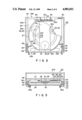
Wafer sampling apparatus (wafer handling apparatus) 20 is under wafer storage room 12. Sampling apparatus 20 is of a drawer type. Drawer 29 of sampling apparatus 20 is provided such that it is drawn out horizontally to the side of wafer probing machine 10. Drawer 29 is loaded with carrier 21 for wafer transfer.
As shown in FIG. 2, drawer 29 of wafer sampling apparatus 20 is accommodated in space 24 defined by square case 20a of a size a little larger than the wafer size. Drawer 29 has at its front a formed recess 29a and at its rear a formed groove 29b for manual operation.
Case 20a is secured to wafer probing machine 10 and has at its front and rear formed first opening 24a and second opening 24b, respectively. To be more specific, wafers are passed through first opening 24a and second opening 24b of case 20a and transferred into the wafer probing machine.
As indicated in FIG. 3, brackets 25 are mounted to the inner side walls of first opening 24a of case 20a with bolts 25a. Each bracket 25 has a set of guide-rollers 26, 27 and 28 to allow drawer 29 to slide in case 20a while being regulated from above, below, left and right. Drawer 29 is held at its peripheral areas from above and below by first guide-rollers 26 and 27 and held also at the lateral edges across the width by a couple of second guide-rollers 28.
As can be seen in FIG. 2, mounted close to second opening 24b of case 20a are ball-catch clamp 31a, 31b and stopper 32 to stop drawer 29 when drawer 29 is pushed in. Stopper 32 is of a screw type and used to slightly adjust the stop position of drawer 29. Stopper 32 connects with drawer 29 at recess 29a. When sensor 39, installed near second opening 24b, finds that drawer 29 has been pushed into case 20a, it sends a detection signal to the handling apparatus in the wafer probing machine.
Another stopper 30 is mounted at the front of drawer 29. As shown in FIG. 4, when drawer 29 is drawn out of case 20a, stopper 30 contacts bracket 25 to stop drawer 29.
As is clear from FIGS. 4 and 5, roller 37a pressurized by spring 37b is fitted to case 20a by bracket 36 and the face of roller 37a is in contact with the underside of drawer 29. Recess 38, which has been formed in the underside of drawer 29, receives roller 37a which falls thereinto pushed by spring 37b when drawer 29 is drawn out, thereby keeping drawer 29 stably in the drawn-out position.
Next, carrier 21 will be described in greater detail.
Carrier 21 is generally a disc and made of a material having low conductivity. Formed in the upper position of carrier 21 are tray portions (wafer-mounting portions) 21d, 21e and 21f and frame portions 21a, 21b and 21c. Wafers of three different sizes can be loaded on portions 21d, 21e and 21f. The inside diameters of frame portions 21a, 21b and 21c are 200 mm, 150 mm and 125 mm respectively.
Notched groove 22 is formed running through the center of carrier 21 from one end to the opposite end of the peripheral edge of carrier 21. As shown in FIG. 3, groove 22 is formed by notching only the upper part of carrier 21 and the bottom of groove 22 is located in a lower position than the lowest step 21d.
As shown in FIG. 2, three taper slideways 35a each having center hole 35 are formed equally spaced at suitable positions of the lower portion of carrier 21. Taper slideways 35a are in a conical form around center holes 35. When carrier 21 is loaded on drawer 29, pin 33 of drawer 29 is guided by taper slideway 35a into center hole 35, allowing carrier 21 to be placed stably at a specified position on drawer 29, as shown in FIG. 3.
Groove 22 of carrier 21 loaded on drawer 29 extends in the loading/unloading direction of drawer 29, as shown in FIGS. 2 and 4.
A description will now be made of the sampling of wafers 16 using the above-mentioned handling apparatus when it is necessary to do manual measurement of individual wafers 16 in storage room 12.
First, the program in the computer system to control the wafer probing machine is changed from one for routine test to another for sampling and the operation of the full-automatic transferring apparatus (not shown) is changed. Thus, the full-automatic transferring apparatus pulls out one wafer 16 from cassette 14 and inserts wafer 16 through second opening 24b into case 20a. The arm of the transferring apparatus, holding wafer 16, moves along groove 22 of carrier 21. When the center of wafer 16 coincides with the center of carrier 21, the advance of the arm is stopped. The arm is lowered, wafer 16 is transferred from the arm onto carrier 21 and then the arm is withdrawn from inside case 20a. Sensor 39 detects wafer 16 on carrier 21, confirming that wafer 16 is ready to be taken out of case 20a.
The operator now puts his hand through first opening 24a into case 20a and takes hold of groove 29b. As the operator pulls drawer 29 toward him, drawer 29 slides smoothly, guided by guide-rollers 26, 27, 28, and is pulled out on the side of first opening 24a. When drawer 29 is pulled out sufficiently, roller 37a catches recess 38 of drawer 29 and stopper 30 contacts bracket 25. Thus, drawer 29 is stopped. Carrier 21, together with wafer 16, is taken out of drawer 29. Wafer 16 held on carrier 21 is taken by the operator to a machine for individual wafer inspection.
With the wafer carrier according to the above embodiment, wafers can be transferred manually without directly touching them and can be prevented effectively from being contaminated. This wafer carrier is capable of manual transfer of wafers of various sizes ranging from 125 to 200 mm.
With the handling apparatus according to the above embodiment, it is possible to take wafer samples from inside the wafer probing machine without using forceps (tweezers). Therefore, damage of wafers due to a fall or collision can be avoided.
When the probing machine made according to this invention is used, wafers can be transferred from the wafer cassette to the sampling case by the full-automatic transferring apparatus under control of a computer system. Therefore, wafer samples can be taken easily and quickly by a simple operation of changing computer programs without relying upon the skilled operator.
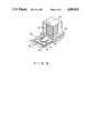
Another embodiment of the wafer handling apparatus according to this invention will be described with reference to FIG. 6.
In wafer handling apparatus 50 according to a second embodiment of this invention, first opening 56 of case 55 is covered by front face portion 51a when drawer 51 is pushed into case 55. Drawer pull 52 attached to front face portion 51a is used to pull out drawer 51 together with carrier 53. Storage room 54 is provided on case 55 of wafer handling apparatus to accommodate a plurality of wafers 16.
According to the above second embodiment, opening 56 of case 55 is closed by drawer 51 when not in use, thus effectively preventing the entry of dust into the machine.
Any apparatus according to the invention, which has been described, can take wafers out of the cassette, one by one, whether the wafers are inspected ones or uninspected ones.
Moreover, any apparatus according to the invention which has been described, can transfer not only semiconductor wafers, but also any other plate-like objects such as printed circuit boards or liquid crystal display panels.
The present invention can apply not only to a wafer probing machine, but also to a heat treatment apparatus (e.g., a dry-etching apparatus, a batch-type CVD apparatus, or an thermal diffusion apparatus), an ion-injecting apparatus, and a resist coating/developing apparatus.
The advantages of this invention will be described in the following:
A wafer carrier according to this invention is suitable for manual transfer in sampling or individual inspection of wafers. Above all, since a carrier is drawn out together with a wafer, a wafer can be transferred by manual operation without directly touching the wafer by hand and, therefore, the wafer is not contaminated. In other words, the wafer carrier according to this invention is suited for manual transfer of wafers from one apparatus to another and can serve as a work interface.
The handling apparatus for wafer carriers according to this invention allows safe and quick sampling of wafers from the wafer probing machine or LCDs from the LCD probing machine one by one.
The probing machine equipped with a handling apparatus for wafer carriers according to this invention allows safety guides sampling wafers one by one without using forceps and, therefore, provides no chances of a wafer falling or colliding with a member of machine. Hence, it is possible to prevent wafers from being damaged during sampling.

Claims (17)

What is claimed is:
1. A water probing machine fitted with a handling apparatus for a wafer carrier, comprising:
a testing section where a multitude of probes are brought into contact with the pads of a device circuit of semiconductor wafers to pass an electric current to the device circuit under test;
a loading/unloading section provided adjacent to said testing section, for automatically taking the semiconductor wafers into and out of said testing section one after another; and
means for transferring the semiconductor wafers between said loading/unloading section and said testing section, and
including:
a sampling case mounted to said loading/unloading section and having formed therein a first opening communicating with the outside of said loading/unloading section and a second opening communicating with the interior of said loading/unloading section;
a drawer adapted to go into and out of said sampling case through the first opening;
means for guiding said drawer between the first opening and the second opening of said sample case;
a carrier which is loaded on said drawer and used to hold one semiconductor wafer at a time comprising:
a tray means for loading thereon the semiconductor wafer submitted to processing, said tray means having a groove which is formed therein for unloading the semiconductor wafer therefrom; and
means for positioning said tray means relative to a predetermined location of the drawer,
whereby, when the carrier having the semiconductor wafer mounted thereon is inserted into the sampling case through the first opening, only the semiconductor wafer is transferred to the loading/unloading section through the second opening by the transferring means.
2. The machine according to claim 1, wherein said tray means have stepped sections constituting a plurality of concentric wafer-mounting surfaces located at different levels.
3. The machine according to claim 1, wherein said groove extends from a peripheral edge of said tray means to at least a central portion of said tray means.
4. The machine according to claim 2, wherein said groove extends to a location lower than the lowest wafer-mounting surface.
5. The carrier according to claim 1, wherein said positioning means includes a plurality of tapered openings formed in the reverse side of said tray means.
6. The machine according to claim 1, wherein the first opening and the second opening of said sampling case face each other.
7. The machine according to claim 1, wherein said drawer comes into contact with a stopper provided in said sampling case when it is drawn out and is thereby stopped.
8. The machine according to claim 7, wherein the stopper is a ball-catch clamp
9. The machine according to claim 7, wherein the stopper has a position adjusting function to vary its position of contact with said drawer.
10. The machine according to claim 1, wherein said wafer carrier has carrier-positioning means on the reverse side of said tray means.
11. The machine according to claim 10, wherein a pin on said drawer fits into a hole of a tapered area on the reverse side of the tray means of the carrier, whereby the carrier is held at a specified position relative to said drawer.
12. The machine according to claim 1, wherein said means for guiding said drawer has guide-rollers.
13. The machine according to claim 12, wherein there are provided a pair of guide-rollers to hold said drawer across the depth and another pair of guide-rollers to hold said drawer across the width.
14. The machine according to claim 12, wherein said drawer has formed on its reverse side a recess, into which a guide-roller pressurized by a coil spring provided on the case will fit when said drawer is drawn out.
15. The machine according to claim 1, wherein said drawer is fitted on its rear side with a stopper, which is held back by a part of the case when said drawer is drawn out, thus causing said drawer to stop at a specified, drawn-out position.
16. The machine according to claim 1, wherein said drawer has formed at its front portion a long groove which serves as a catch for use in manual operation.
17. The machine according to claim 1, wherein the front portion of said drawer defines a L-like configuration in the longitudinal cross section, the L-like bent portion of said drawer being capable of closing the first opening of the case when said drawer is pushed in.
US07/267,375 1988-11-04 1988-11-04 Carrier for transferring plate-like objects one by one, a handling apparatus for loading or unloading the carrier, and a wafer probing machine fitted with the handling apparatus for the wafer carrier Expired - Lifetime US4901011A (en)

Priority Applications (1)

Application Number Priority Date Filing Date Title
US07/267,375 US4901011A (en) 1988-11-04 1988-11-04 Carrier for transferring plate-like objects one by one, a handling apparatus for loading or unloading the carrier, and a wafer probing machine fitted with the handling apparatus for the wafer carrier

Applications Claiming Priority (1)

Application Number Priority Date Filing Date Title
US07/267,375 US4901011A (en) 1988-11-04 1988-11-04 Carrier for transferring plate-like objects one by one, a handling apparatus for loading or unloading the carrier, and a wafer probing machine fitted with the handling apparatus for the wafer carrier

Publications (1)

Publication Number Publication Date
US4901011A true US4901011A (en) 1990-02-13

Family

ID=23018518

Family Applications (1)

Application Number Title Priority Date Filing Date
US07/267,375 Expired - Lifetime US4901011A (en) 1988-11-04 1988-11-04 Carrier for transferring plate-like objects one by one, a handling apparatus for loading or unloading the carrier, and a wafer probing machine fitted with the handling apparatus for the wafer carrier

Country Status (1)

Country Link
US (1) US4901011A (en)

Cited By (21)

* Cited by examiner, † Cited by third party
Publication number Priority date Publication date Assignee Title
US4950982A (en) * 1987-11-30 1990-08-21 Tokyo Electron Limited Electric probing test machine
US5317257A (en) * 1990-11-28 1994-05-31 Mitsubishi Denki Kabushiki Kaisha Burn-in apparatus and burn-in board removing method using movable cooling enclosure
US5339952A (en) * 1992-06-19 1994-08-23 International Business Machines Corporation Transfer container for transferring flimsy circuit panels under clean room conditions
US5364225A (en) * 1992-06-19 1994-11-15 Ibm Method of printed circuit panel manufacture
US5382127A (en) * 1992-08-04 1995-01-17 International Business Machines Corporation Pressurized interface apparatus for transferring a semiconductor wafer between a pressurized sealable transportable container and a processing equipment
US5395198A (en) * 1992-06-19 1995-03-07 International Business Machines Corporation Vacuum loading chuck and fixture for flexible printed circuit panels
US5445486A (en) * 1992-03-29 1995-08-29 Tokyo Electron Sagami Limited Substrate transferring apparatus
US5451131A (en) * 1992-06-19 1995-09-19 International Business Machines Corporation Dockable interface airlock between process enclosure and interprocess transfer container
US5509772A (en) * 1992-01-16 1996-04-23 Commissariat A L'energie Atomique System for the handling and confinement of flat objects in individual boxes
US5604443A (en) * 1994-05-23 1997-02-18 Tokyo Electron Limited Probe test apparatus
US6104184A (en) * 1997-11-17 2000-08-15 Taiwan Semiconductor Manufacturing Company, Ltd. Method and apparatus for loading a wafer into a test machine
US6366102B1 (en) * 1997-05-14 2002-04-02 Tokyo Seimitsu Co., Ltd. Wafer probing machine
US20020053734A1 (en) * 1993-11-16 2002-05-09 Formfactor, Inc. Probe card assembly and kit, and methods of making same
US6811370B2 (en) * 1999-03-25 2004-11-02 N&K Technology, Inc. Wafer handling robot having X-Y stage for wafer handling and positioning
FR2888987A1 (en) * 2005-07-20 2007-01-26 St Microelectronics Sa Silicon wafer maintaining system for wafer probing machine, has removable plate for receiving wafer, and support element receiving removable plate, where external diameter of plate is greater than diameter of wafer
US20070041812A1 (en) * 2004-09-27 2007-02-22 Mitsubishi Denki Kabushiki Kaisha Semiconductor manufacturing equipment and semiconductor manufacturing method
US20080007471A1 (en) * 2004-10-08 2008-01-10 Goldberg Mark R Rf receiving and transmitting apparatuses having a microstrip-slot log-periodic antenna
US20080152922A1 (en) * 2006-12-21 2008-06-26 Wing Lau Cheng Hybrid composite wafer carrier for wet clean equipment
US20110185387A1 (en) * 1995-10-02 2011-07-28 Starsight Telecast, Inc. Systems and methods for contextually linking television program information
US20120146277A1 (en) * 2010-12-14 2012-06-14 Foxconn Advanced Technology Inc. Clamping apparatus
US20140037406A1 (en) * 2012-07-31 2014-02-06 Shenzhen China Star Optoelectronics Technology Co. Ltd. Glass Substrate Cassette and Pick-and-Place System for Glass Substrate

Citations (4)

* Cited by examiner, † Cited by third party
Publication number Priority date Publication date Assignee Title
US4534389A (en) * 1984-03-29 1985-08-13 Hewlett-Packard Company Interlocking door latch for dockable interface for integrated circuit processing
US4755746A (en) * 1985-04-24 1988-07-05 Prometrix Corporation Apparatus and methods for semiconductor wafer testing
US4759008A (en) * 1986-10-02 1988-07-19 Pioneer Electronic Corporation Loading mechanism for disk player
US4797865A (en) * 1986-06-02 1989-01-10 Victor Company Of Japan, Ltd. Information recording disc player having receiving parts for receiving a plurality of disc cartridges

Patent Citations (4)

* Cited by examiner, † Cited by third party
Publication number Priority date Publication date Assignee Title
US4534389A (en) * 1984-03-29 1985-08-13 Hewlett-Packard Company Interlocking door latch for dockable interface for integrated circuit processing
US4755746A (en) * 1985-04-24 1988-07-05 Prometrix Corporation Apparatus and methods for semiconductor wafer testing
US4797865A (en) * 1986-06-02 1989-01-10 Victor Company Of Japan, Ltd. Information recording disc player having receiving parts for receiving a plurality of disc cartridges
US4759008A (en) * 1986-10-02 1988-07-19 Pioneer Electronic Corporation Loading mechanism for disk player

Cited By (30)

* Cited by examiner, † Cited by third party
Publication number Priority date Publication date Assignee Title
US4950982A (en) * 1987-11-30 1990-08-21 Tokyo Electron Limited Electric probing test machine
US5317257A (en) * 1990-11-28 1994-05-31 Mitsubishi Denki Kabushiki Kaisha Burn-in apparatus and burn-in board removing method using movable cooling enclosure
US5509772A (en) * 1992-01-16 1996-04-23 Commissariat A L'energie Atomique System for the handling and confinement of flat objects in individual boxes
US5445486A (en) * 1992-03-29 1995-08-29 Tokyo Electron Sagami Limited Substrate transferring apparatus
US5339952A (en) * 1992-06-19 1994-08-23 International Business Machines Corporation Transfer container for transferring flimsy circuit panels under clean room conditions
US5364225A (en) * 1992-06-19 1994-11-15 Ibm Method of printed circuit panel manufacture
US5395198A (en) * 1992-06-19 1995-03-07 International Business Machines Corporation Vacuum loading chuck and fixture for flexible printed circuit panels
US5451131A (en) * 1992-06-19 1995-09-19 International Business Machines Corporation Dockable interface airlock between process enclosure and interprocess transfer container
US5382127A (en) * 1992-08-04 1995-01-17 International Business Machines Corporation Pressurized interface apparatus for transferring a semiconductor wafer between a pressurized sealable transportable container and a processing equipment
US20020053734A1 (en) * 1993-11-16 2002-05-09 Formfactor, Inc. Probe card assembly and kit, and methods of making same
US8373428B2 (en) 1993-11-16 2013-02-12 Formfactor, Inc. Probe card assembly and kit, and methods of making same
US5604443A (en) * 1994-05-23 1997-02-18 Tokyo Electron Limited Probe test apparatus
US20110185387A1 (en) * 1995-10-02 2011-07-28 Starsight Telecast, Inc. Systems and methods for contextually linking television program information
US6366102B1 (en) * 1997-05-14 2002-04-02 Tokyo Seimitsu Co., Ltd. Wafer probing machine
US6104184A (en) * 1997-11-17 2000-08-15 Taiwan Semiconductor Manufacturing Company, Ltd. Method and apparatus for loading a wafer into a test machine
US6811370B2 (en) * 1999-03-25 2004-11-02 N&K Technology, Inc. Wafer handling robot having X-Y stage for wafer handling and positioning
US7994067B2 (en) * 2004-09-27 2011-08-09 Mitsubishi Denki Kabushiki Kaisha Semiconductor manufacturing equipment with an open-topped cassette apparatus
US20070041812A1 (en) * 2004-09-27 2007-02-22 Mitsubishi Denki Kabushiki Kaisha Semiconductor manufacturing equipment and semiconductor manufacturing method
CN100405569C (en) * 2004-09-27 2008-07-23 三菱电机株式会社 Semiconductor manufacturing device and semiconductor manufacturing method
US7583233B2 (en) * 2004-10-08 2009-09-01 Alliant Techsystems Inc. RF Receiving and transmitting apparatuses having a microstrip-slot log-periodic antenna
US20080007471A1 (en) * 2004-10-08 2008-01-10 Goldberg Mark R Rf receiving and transmitting apparatuses having a microstrip-slot log-periodic antenna
FR2888987A1 (en) * 2005-07-20 2007-01-26 St Microelectronics Sa Silicon wafer maintaining system for wafer probing machine, has removable plate for receiving wafer, and support element receiving removable plate, where external diameter of plate is greater than diameter of wafer
US8146902B2 (en) * 2006-12-21 2012-04-03 Lam Research Corporation Hybrid composite wafer carrier for wet clean equipment
US20120168079A1 (en) * 2006-12-21 2012-07-05 Lam Research Corporation Method for Manufacturing a Hybrid Composite Wafer Carrier for Wet Clean Equipment
US8292697B2 (en) * 2006-12-21 2012-10-23 Lam Research Corporation Method for manufacturing a hybrid composite wafer carrier for wet clean equipment
US20080152922A1 (en) * 2006-12-21 2008-06-26 Wing Lau Cheng Hybrid composite wafer carrier for wet clean equipment
US20120146277A1 (en) * 2010-12-14 2012-06-14 Foxconn Advanced Technology Inc. Clamping apparatus
US8454005B2 (en) * 2010-12-14 2013-06-04 Zhen Ding Technology Co., Ltd. Clamping apparatus
US20140037406A1 (en) * 2012-07-31 2014-02-06 Shenzhen China Star Optoelectronics Technology Co. Ltd. Glass Substrate Cassette and Pick-and-Place System for Glass Substrate
US9079714B2 (en) * 2012-07-31 2015-07-14 Shenzhen China Star Optoelectronics Technology Co., Ltd Glass substrate cassette and pick-and-place system for glass substrate

Similar Documents

Publication Publication Date Title
US4901011A (en) Carrier for transferring plate-like objects one by one, a handling apparatus for loading or unloading the carrier, and a wafer probing machine fitted with the handling apparatus for the wafer carrier
US4938654A (en) Automated wafer inspection system
US5246218A (en) Apparatus for securing an automatically loaded wafer cassette on a wafer processing equipment
US6070731A (en) IC receiving tray storage device and mounting apparatus for the same
US4818169A (en) Automated wafer inspection system
US4789294A (en) Wafer handling apparatus and method
US6830651B2 (en) Load port capable of coping with different types of cassette containing substrates to be processed
KR101158064B1 (en) Electronic component testing equipment and method of testing electronic component
US6404212B1 (en) Testing of BGA and other CSP packages using probing techniques
KR100248561B1 (en) Probe system
KR20070056993A (en) Rinse processing method, developing processing apparatus, and computer readable medium encoded with a control program to be executed by a computer
KR20060019572A (en) Transportation device, electronic component-handling device, and transportation method in electronic component-handling device
KR20030063215A (en) Method of determining retreat permission position of carrier arm and teaching device thereof
US5086270A (en) Probe apparatus
JPH0370900B2 (en)
JP3099183B2 (en) Wafer probing machine
KR970008328B1 (en) Carrier fro transferring plate-like objects one by one, a handling apparatus for loading or unloading the carrier, and a wafer probing machine
JPH0354843A (en) Semiconductor manufacturing device
JPH0333062Y2 (en)
JPH0732175B2 (en) Probe device with automatic probe card exchange function
JPS5832267Y2 (en) Push-up tool for substrate holder
JPH0878497A (en) Transferring apparatus
JP2665886B2 (en) Probe device
JPH10116890A (en) Single wafer cassette
JP2500006B2 (en) Wafer extractor

Legal Events

Date Code Title Description
AS Assignment

Owner name: TOKYO ELECTRON LIMITED,, JAPAN

Free format text: ASSIGNMENT OF ASSIGNORS INTEREST.;ASSIGNORS:KOIKE, HISASHI;TANAKA, SUMI;REEL/FRAME:005196/0883

Effective date: 19881025

STCF Information on status: patent grant

Free format text: PATENTED CASE

FEPP Fee payment procedure

Free format text: PAYOR NUMBER ASSIGNED (ORIGINAL EVENT CODE: ASPN); ENTITY STATUS OF PATENT OWNER: LARGE ENTITY

FPAY Fee payment

Year of fee payment: 4

FPAY Fee payment

Year of fee payment: 8

FEPP Fee payment procedure

Free format text: PAYOR NUMBER ASSIGNED (ORIGINAL EVENT CODE: ASPN); ENTITY STATUS OF PATENT OWNER: LARGE ENTITY

Free format text: PAYER NUMBER DE-ASSIGNED (ORIGINAL EVENT CODE: RMPN); ENTITY STATUS OF PATENT OWNER: LARGE ENTITY

FPAY Fee payment

Year of fee payment: 12