US4900948A - Apparatus providing signals for burn-in of integrated circuits - Google Patents
Apparatus providing signals for burn-in of integrated circuits Download PDFInfo
- Publication number
- US4900948A US4900948A US07/168,875 US16887588A US4900948A US 4900948 A US4900948 A US 4900948A US 16887588 A US16887588 A US 16887588A US 4900948 A US4900948 A US 4900948A
- Authority
- US
- United States
- Prior art keywords
- board
- contacts
- burn
- auxiliary
- edge
- Prior art date
- Legal status (The legal status is an assumption and is not a legal conclusion. Google has not performed a legal analysis and makes no representation as to the accuracy of the status listed.)
- Expired - Lifetime
Links
Images

Classifications
-
- G—PHYSICS
- G01—MEASURING; TESTING
- G01R—MEASURING ELECTRIC VARIABLES; MEASURING MAGNETIC VARIABLES
- G01R31/00—Arrangements for testing electric properties; Arrangements for locating electric faults; Arrangements for electrical testing characterised by what is being tested not provided for elsewhere
- G01R31/28—Testing of electronic circuits, e.g. by signal tracer
- G01R31/2851—Testing of integrated circuits [IC]
- G01R31/2855—Environmental, reliability or burn-in testing
- G01R31/286—External aspects, e.g. related to chambers, contacting devices or handlers
- G01R31/2863—Contacting devices, e.g. sockets, burn-in boards or mounting fixtures
-
- H—ELECTRICITY
- H05—ELECTRIC TECHNIQUES NOT OTHERWISE PROVIDED FOR
- H05K—PRINTED CIRCUITS; CASINGS OR CONSTRUCTIONAL DETAILS OF ELECTRIC APPARATUS; MANUFACTURE OF ASSEMBLAGES OF ELECTRICAL COMPONENTS
- H05K7/00—Constructional details common to different types of electric apparatus
- H05K7/14—Mounting supporting structure in casing or on frame or rack
- H05K7/1438—Back panels or connecting means therefor; Terminals; Coding means to avoid wrong insertion
- H05K7/1439—Back panel mother boards
- H05K7/1445—Back panel mother boards with double-sided connections
Definitions
- the present invention relates to an arrangement for connecting discrete circuit packages for burn-in in an automatic burn-in environmental system requiring a large number of connections to a burn-in board using standard connectors and environmental chambers.
- Typical automatic burn-in and environmental systems are manufactured by Micro Control Company, the assignee of the present application, having an office at 7956 Main Street N.E., Minneapolis, Minn. 55432.
- An existing system is described in Micro Control Company Publication No. 990078, which shows a typical environmental chamber and describes various specifications for driver/receiver boards utilizing existing 128 contact card edge connectors between the driver/receiver boards and the "burn-in boards" that are utilized for supporting or mounting the digital devices to be tested.
- U.S. Pat. No. 4,468,616 shows testing equipment for electronic components, that has a type of an interconnecting board or span board between the burn-in boards and driver boards.
- the burn-in boards are shown at 12, and the driver boards are shown at 13, and a printed wire board 15 that has a plane that is perpendicular to the planes of the driver boards and burn-in boards carries paired spaced connectors or jacks 16 and 17.
- the paired spaced jacks are connected by conductor pins 20. This is therefore a transition board to carry the connections between the driver board and the burn-in boards in an environmental chamber in which the burn-in boards are mounted.
- U.S. Pat. No. 3,147,054 to Alexander et al. shows a test point extender for circuit boards that has a wraparound sheet that folds around a circuit board so a fold line of the sheet as at one edge of the circuit board and both ends of the folded sheet are at the opposite edge of the circuit board.
- the sheet has conductors that engage contacts on the one end of the board (where the fold is) and which carry electrical signals back to the connectors on the wraparound sheet at the other end of the circuit board from the test connections. This is for making the normal connections to a circuit board at an opposite end of the board from the contacts on the board.
- German Publication No. 2811775 briefly describes a testing device for printed circuits which uses test probes.
- a typical environmental chamber is shown in U.S. Pat. No. 4,374,317, which illustrates a typical slotted wall through which ends of burn-in boards pass for test connections on the exterior of the environmental chamber.
- the present invention relates to a burn-in system that provides burn-in boards that have parallel edge connectors to permit doubling the number of driver/receiver boards that can be connected to one burn-in board for testing electronic circuit package, components, primarily digital devices such as VLSI chips, without modifying or changing from standard edge connectors on the driver/receiver boards and without changing the construction of environmental chambers used for the burn-in system.
- a narrow temperate zone or chamber is included in some environmental chambers adjacent to one wall of the environmental chamber (which normally is an oven).
- the temperate chamber is defined by a second wall spaced from the environmental chamber wall, and the edges of the burn-in board which carry the contacts for connection to conditioning and control circuitry span this temperate chamber so that the edge connectors utilized not only are on the exterior of the environmental chamber wall but are spaced from the environmental chamber wall by a distance that provides for a substantial reduction in temperature at the connectors.
- the second wall forming the temperate chamber also has slots in it.
- Burn-in boards extending through slots of the environmental chamber wall from the interior of the environmental chamber also extend across the temperate chamber and through the slots in the second wall to the exterior where the burn-in boards are coupled to standard multiple contact card edge connectors or jacks.
- the burn-in board contacts are coupled through the edge connectors to selected driver/receiver boards that are supported relative to the environmental chamber.
- driver/receiver (stimulation and control) boards which are used for providing controlled, programmed standard signals to stimulate the contacts on the circuit packages and receiving return signals from the digital devices thereon have a set number of edge contacts that are coupled to the burn-in board through the standard card edge jacks or connectors.
- the edge jacks or connectors generally are provided with 100 pins each for a total of 200 pins when two connectors are used.
- 128 of these pins are used as driver-receiver connections on the burn-in board using two vertically aligned edge connectors. The rest of the pins are used for miscellaneous purposes, such as ground and control lines.
- an auxiliary board is mounted on a main burn-in board which has the circuit packages, either analog or digital devices mounted thereon, but is spaced from the main burn-in board and extends parallel to the main board.
- the auxiliary board also extends from the interior of the environmental chamber and across the temperate chamber (if one is present) to the exterior.
- the auxiliary board has the same number of contacts on its outer edge as that of a standard driver/receiver board.
- the auxiliary board is spaced from the burn-in board on which it is mounted by the standard spacing used for the slots in the environmental chamber through which the burn-in boards extend to the exterior.
- the contacts on the auxiliary board which as stated is parallel to the burn-in board, are connected to suitable conductors on the auxiliary board and the conductors are jumpered to terminals or conductors on the main burn-in board for connection to circuit packages.
- the assembly permits using existing environmental chambers, so that the size of the chamber for supporting both the burn-in boards and the driver/receiver boards does not have to change, and standard driver/receiver boards can also be used for providing a controlled program for stimulating the connections of circuits in the circuit packages on the burn-in board.
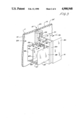
- FIG. 1 is a top plan view of a typical environmental system in which the burn-in boards of the present invention can be used;
- FIG. 2 is a front schematic elevational view of the environmental system of FIG. 1;
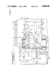
- FIG. 3 is a perspective view of typical interior and exterior board or card cages used for supporting burn-in boards and the driver/receiver boards, with a typical burn-in board made according to the present invention illustrated schematically in place;
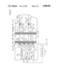
- FIG. 4 is a fragmentary side view of a typical burn-in board arrangement, with parts in section and parts broken away, and viewed from an opposite side from the view shown in FIG. 3;
- FIG. 5 is a top sectional view taken generally along lines 5--5 in FIG. 4.
- an environmental test system is shown generally at 10 and includes a main environmental chamber housing or oven 11, a driver/receiver loading chamber housing 12, and a console assembly 13 on which a control computer 14 is supported.
- the control computer 14 has the necessary programs for controlling the driver/receiver boards mounted in the loading chamber housing 12, to provide for the tests to be conducted on circuit packaging which can be analog or digital, but which will be primarily digital devices, such as VLSI chips, connected on burn-in boards in the environmental chamber housing 11.
- the environmental chamber housing 11 in front view, shows a loading door 17, with suitable environmental temperature controls 15 thereon, along with desired indicators.
- the environmental chamber housing has an interior chamber that can be temperature and humidity controlled.
- a power supply rack 16 is used for supporting the environmental chamber housing 11. This compact arrangement can be driven with a personal computer such as that shown at 14 to control and program the signals to the circuit packages on the various burn-in boards. As will be seen, a plurality of burn-in boards can be placed in an interior environmental chamber in housing 11.
- the conventional burn-in board chamber and loading chamber of the system 10 is shown in FIG. 3, with the exterior walls broken away to show the interior cages for supporting the boards.
- the environmental chamber housing 11 defines an interior heated environmental chamber 20, surrounded by side walls 21 arranged in a desired manner.
- a housing 22 is positioned at the end of the interior chamber 20 opposite from the loading door 17 .
- Housing 22, as shown, forms a temperate zone or chamber 23 that separates the burn-in board interior environmental chamber 20 from the driver/receiver board chamber 24 of the load chamber housing 12.
- the schematic showing includes a burn-in board rack indicated generally at 25 (also called a card cage), which is within the interior environmental chamber 20 of the environmental chamber housing 11.
- the rack 25 has a bottom wall 26 and suitable guide members shown at 27 therein for receiving the edges of burn-in boards, or, if desired, for receiving separate loading racks holding several burn-in boards.
- the rack 25 has side walls 28,28 that mount suitable components such as that shown at 29 for supporting the burn-in boards in the proper orientation.
- the driver/receiver board chamber 24 has an exterior card cage or rack 30 mounted therein in a suitable manner on the interior of the walls forming the loading chamber housing 12.
- the exterior driver/receiver board rack or cage 30 has side walls 31 that are used for guiding and supporting a bottom wall 31A (FIG. 4) that will support driver/receiver boards of conventional design as they are inserted in direction as indicated by the arrow 32.
- the temperate zone housing 22 is defined by an end environmental chamber wall 34 that has slots 35 defined therein, and these slots 35 are of size to receive a burn-in board assembly shown at 40 that is supported in a suitable guide 27, and is slid in direction as indicated by the arrow 41 from the front of the burn-in chamber 11.
- the end portions of the burn-in board assembly which has contacts thereon for connection to driver/receiver boards is slid through the slots 35, and across the temperate zone chamber 23 and then through additional slots shown in FIG. 5 at 44, in a rear wall assembly 43 of the temperate zone housing 22.
- the temperate zone housing 22 is constructed so there will be a sealing gasket of rubber material on the planar side surfaces of each of the burn-in board portions that pass through the respective slots.
- the end wall 34 of the environmental chamber is made of a sandwich construction comprising a pair of sheets or layers 34A of rigid to semi-rigid material, and a central silicon rubber sheet 34B (or other flexible sealing material) sandwiched between sheets 34A and held in place.
- the silicon rubber material 34B has slits aligning with the respective slots 35 which are formed in the sheets 34a.
- the edge of the slots in the sheets 34A are spaced enough so the portion of the rubber sheet adjacent the slot edges will be permitted to yield sufficiently to permit a flat, generally narrow board, such as a burn-in board, to slide through the slit.
- the rubber forming the sides of the slit resiliently engages the sides of such a planar board to seal against the board side surfaces.
- the wall 43 is made in the same way with outer panels or sheets 43A sandwiching a silicon rubber sheet 43B that has slits aligning with the slots 44. The edges of the slits in the rubber sheet sides will yield and seal against a board slid through the slot.
- the temperate zone housing does have side walls 50, and a top wall 51 and a bottom wall 51A for enclosing the temperate chamber and keeping such temperate chamber isolated from the interior environmental chamber 20 and from the exterior as well.
- the walls 21 for example, forming the environmental chamber 20 can be made of a suitable insulating material, as desired, and are shown only schematically.
- Standard card edge connectors or jacks shown schematically at 52 are mounted onto driver/receiver boards 55 to the outer side of the wall 43 that is the exterior wall of the environmental system.
- the connectors 52 have receptacles and contacts for receiving the edges of circuit cards or boards.
- the connectors 52 are positioned to have the receptacles align with the exterior of the slots 44.
- the contacts in the connectors 52 are connected to conductors on the driver/receiver boards 55 and are fixed to the edge of the driver/receiver boards.
- the driver/receiver boards are supported on the card or board support rack 30.
- there are vertically stacked pairs of jacks or connectors 52 and in the typical environmental chamber system shown in FIG. 3 the vertical length of the slots 44, is such that two connectors 52 are aligned with each slot and provide for 128 board edge contacts to be connected at each of the slots.
- Driver/receiver boards 55 are thus presently made up to provide for 128 contacts for burn-in purposes, and in addition are made to transfer power through separate connectors to power the burn-in boards and the components that are present on the burn-in boards.
- Burn-in board assembly 40 of the present form of the invention comprises a first generally planar circuit board or card 60 that is made of a suitable material, and which has connector receptacles for receiving pairs of a plurality of circuit packages or components shown at 61 schematically.
- the circuit packages may be various dual inline packages such as ROM, RAM, PROM, EPROM, SSI, MSI, LSI AND VLSI devices.
- the VLSI devices are ones which require a high number of connectors or pins for burn-in. Special drivers, multiplexers, device loads and the like can be applied from the driver/receiver boards. In order to utilize the high performance signal providing systems necessary, it requires several hundred driver/receiver connections to the circuit package components on the burn-in board.
- the board assembly 40 has an auxiliary connector board 65, also made of a suitable material, which is positioned spaced from the main or first board 60 and which is fixedly mounted on the board 60.
- the auxiliary board 65 is parallel to the main board 60.
- the auxiliary board 65 is substantially identical in vertical height and thickness dimensions to the end portion of the main board 60, and has suitable edge contacts 66 thereon on one edge thereof, which are positioned to mate with the existing circuit card edge connectors 52.
- the auxiliary board 65 is fixedly supported on the main board 60 with a mounting strip or block 68 that is fixed to the main board 60 and positions the auxiliary board 65 at a spacing from the plane of the main board 60 equal to the spacing between the slots 35 and thus equal to the spacing between the slots 44 formed in walls 34 and 43, respectively.
- the edge contacts 66 on auxiliary board 65 are connected to suitable printed wire conductors 70, which are formed on the auxiliary board 65, and at the inner edge 71 of the auxiliary board 65, there are flexible jumpers 72 electrically and mechanically connected to each of the printed conductors 70, and in turn, the jumpers 72 are soldered or connected to suitable terminals 73 on the main board 60.
- the main board 60 has printed wire conductors 76 thereon which are electrically connected to individual contacts 74 on the edge of the main board 60 extending into slots 44, thus some printed wire conductors on board 60 are connected to contacts 74 and some are connected through jumpers 72 and edge contacts 66 on auxiliary board 65.
- the same standard edge connectors 52 can be used for both the main board 60 and auxiliary board 65 for connection simultaneously through the circuit edge connectors 52 at adjacent slots 44.
- More than one auxiliary board can be used on each main burn-in board. For example, there can be an auxiliary board on each side of the main board.
- the auxiliary boards permit the connection of two (or more) driver/receiver boards 55A and 55B, to the same burn-in board assembly 40 to stimulate the contacts of the circuit package or components 61 on this burn-in board assembly in a desired manner using the added number of connections from at least two separate driver/receiver boards such as those shown at 55A and 55B.
- the driver/receiver boards 55A and 55B provide for the necessary coupling from various operational and control components thereon, which are shown only schematically at 75, and these then in turn can be connected and programmed to provide signals to the circuit packages 61 through suitable controls 79 operated from the microcomputer or personal computer 77, as programmed with suitable software 78.
- the particular operation sequence being conducted on the circuits in the circuit packages 61 can be selected by the user, and the individual connections or connecting pins of each of the circuit packages 61, which are shown at 61A in FIG. 5, then can be connected to receive signals through separate conductors and connectors, including conductors to the desired driver/receiver boards.
- FIG. 4 For power connection between the driver/receiver board and the burn-in boards, conventional connections are shown in FIG. 4.
- An edge connector 52A is used and a connector board 82 extends into connector 52A for coupling contacts 83 on the main and auxiliary boards 60 and 55 to power.
- the power is carried on contacts 81 on the respective driver/receiver boards 55A and 55B across a conventional back plane 84.
- the power connections are conventional except for use of the auxiliary board.
- the burn-in operation provides a stimulation signal to each of the connectors or pins 61A of the circuit packages, which are generally digital devices, and the results of such stimulation are received by the controls to insure the circuit in the package is operating.
- temperate zone or chamber While a temperate zone or chamber is shown, many environmental chambers have card slots in a single exterior wall for permitting connections to be made to interior burn-in boards.
Abstract
Description
Claims (10)
Priority Applications (1)
| Application Number | Priority Date | Filing Date | Title |
|---|---|---|---|
| US07/168,875 US4900948A (en) | 1988-03-16 | 1988-03-16 | Apparatus providing signals for burn-in of integrated circuits |
Applications Claiming Priority (1)
| Application Number | Priority Date | Filing Date | Title |
|---|---|---|---|
| US07/168,875 US4900948A (en) | 1988-03-16 | 1988-03-16 | Apparatus providing signals for burn-in of integrated circuits |
Publications (1)
| Publication Number | Publication Date |
|---|---|
| US4900948A true US4900948A (en) | 1990-02-13 |
Family
ID=22613313
Family Applications (1)
| Application Number | Title | Priority Date | Filing Date |
|---|---|---|---|
| US07/168,875 Expired - Lifetime US4900948A (en) | 1988-03-16 | 1988-03-16 | Apparatus providing signals for burn-in of integrated circuits |
Country Status (1)
| Country | Link |
|---|---|
| US (1) | US4900948A (en) |
Cited By (27)
| Publication number | Priority date | Publication date | Assignee | Title |
|---|---|---|---|---|
| US4997366A (en) * | 1990-02-05 | 1991-03-05 | Micro Control Company | Rear wall construction for burn-in environmental systems |
| US5023754A (en) * | 1990-01-19 | 1991-06-11 | International Business Machines Corporation | Double-sided backplane assembly |
| US5086271A (en) * | 1990-01-12 | 1992-02-04 | Reliability Incorporated | Driver system and distributed transmission line network for driving devices under test |
| US5157829A (en) * | 1990-10-02 | 1992-10-27 | Outboard Marine Corporation | Method of burn-in testing of circuitry |
| US5164661A (en) * | 1991-05-31 | 1992-11-17 | Ej Systems, Inc. | Thermal control system for a semi-conductor burn-in |
| US5200885A (en) * | 1990-04-26 | 1993-04-06 | Micro Control Company | Double burn-in board assembly |
| US5311408A (en) * | 1991-08-09 | 1994-05-10 | Tandem Computers, Incorporated | Electronic assembly with improved grounding and EMI shielding |
| US5402078A (en) * | 1992-10-13 | 1995-03-28 | Micro Control Company | Interconnection system for burn-in boards |
| US5430615A (en) * | 1990-08-14 | 1995-07-04 | The Grass Valley Group, Inc. | Printed circuit board assembly |
| EP0731992A1 (en) * | 1993-12-01 | 1996-09-18 | Aehr Test Systems, Inc. | High-density interconnect technique |
| US5798653A (en) * | 1995-04-20 | 1998-08-25 | Sun Microsystems, Inc. | Burn-in system for reliable integrated circuit manufacturing |
| US5880592A (en) * | 1993-07-15 | 1999-03-09 | Micron Technology, Inc. | Modular design for an IC testing burn-in oven |
| US5911897A (en) * | 1997-01-13 | 1999-06-15 | Micro Control Company | Temperature control for high power burn-in for integrated circuits |
| US5923098A (en) * | 1997-10-03 | 1999-07-13 | Micro Control Company | Driver board having stored calibration data |
| WO2000011487A1 (en) * | 1998-08-19 | 2000-03-02 | Eles Equipment S.R.L. | Equipment for performing electrical and environmental tests on semiconductor electronic devices |
| WO2000037950A1 (en) * | 1998-12-21 | 2000-06-29 | Kaitech Engineering, Inc. | Lead frame structure for testing integrated circuits |
| US6114866A (en) * | 1997-09-08 | 2000-09-05 | Mitsubishi Electric Systems Lsi Design Corporation | Semiconductor device test board and method for evaluating semiconductor devices |
| US6137301A (en) * | 1998-05-11 | 2000-10-24 | Vanguard International Semiconductor Company | EPROM used as a voltage monitor for semiconductor burn-in |
| US6158030A (en) * | 1998-08-21 | 2000-12-05 | Micron Technology, Inc. | System and method for aligning output signals in massively parallel testers and other electronic devices |
| US6175498B1 (en) | 1999-07-13 | 2001-01-16 | Micro Control Company | Burn-in board and heat sink assembly mounting rack |
| US6288371B1 (en) | 1999-07-13 | 2001-09-11 | Micro Control Company | Temperature controlled high power burn-in board heat sinks |
| US6472895B2 (en) * | 2000-12-06 | 2002-10-29 | Advanced Micro Devices, Inc. | Method and system for adapting burn-in boards to multiple burn-in systems |
| WO2003048793A1 (en) * | 2001-11-29 | 2003-06-12 | Denselight Semiconductors Pte Ltd | Method of construction for high density, adaptable burn-in tool |
| US20030184035A1 (en) * | 2002-04-01 | 2003-10-02 | Hyo-Sun Yu | Cart for electric or electronic devices having a testing function |
| US6690188B2 (en) | 1998-07-28 | 2004-02-10 | Micron Technology, Inc. | Method of testing a semiconductor device |
| US20040112581A1 (en) * | 2002-12-17 | 2004-06-17 | Hamilton Harold E. | Burn-in oven heat exchanger having improved thermal conduction |
| US20040182564A1 (en) * | 2002-12-17 | 2004-09-23 | Micro Control Company | Heat exchange system chip temperature sensor |
Citations (9)
| Publication number | Priority date | Publication date | Assignee | Title |
|---|---|---|---|---|
| US3147054A (en) * | 1962-06-14 | 1964-09-01 | Rca Corp | Test point extender for circuit boards |
| US3736471A (en) * | 1970-11-18 | 1973-05-29 | I Honeywell Bull Soc | Assemblage element for functional unit with card connector means |
| US4132948A (en) * | 1977-03-17 | 1979-01-02 | Teradyne, Inc. | Test fixture using stock printed circuit board having test pins mounted thereon |
| US4145620A (en) * | 1977-10-05 | 1979-03-20 | Serel Corporation | Modular dynamic burn-in apparatus |
| US4374317A (en) * | 1979-07-05 | 1983-02-15 | Reliability, Inc. | Burn-in chamber |
| US4468616A (en) * | 1980-08-29 | 1984-08-28 | Fujitsu Limited | Testing equipment for electric components |
| US4514786A (en) * | 1981-07-10 | 1985-04-30 | Thomson-Csf | Integrated-circuit support device employed in a system for selecting high-reliability integrated circuits |
| US4516071A (en) * | 1982-07-26 | 1985-05-07 | The United States Of America As Represented By The Administration Of The United States National Aeronautics And Space Administration | Split-cross-bridge resistor for testing for proper fabrication of integrated circuits |
| US4636726A (en) * | 1982-01-04 | 1987-01-13 | Artronics Corporation | Electronic burn-in system |
-
1988
- 1988-03-16 US US07/168,875 patent/US4900948A/en not_active Expired - Lifetime
Patent Citations (9)
| Publication number | Priority date | Publication date | Assignee | Title |
|---|---|---|---|---|
| US3147054A (en) * | 1962-06-14 | 1964-09-01 | Rca Corp | Test point extender for circuit boards |
| US3736471A (en) * | 1970-11-18 | 1973-05-29 | I Honeywell Bull Soc | Assemblage element for functional unit with card connector means |
| US4132948A (en) * | 1977-03-17 | 1979-01-02 | Teradyne, Inc. | Test fixture using stock printed circuit board having test pins mounted thereon |
| US4145620A (en) * | 1977-10-05 | 1979-03-20 | Serel Corporation | Modular dynamic burn-in apparatus |
| US4374317A (en) * | 1979-07-05 | 1983-02-15 | Reliability, Inc. | Burn-in chamber |
| US4468616A (en) * | 1980-08-29 | 1984-08-28 | Fujitsu Limited | Testing equipment for electric components |
| US4514786A (en) * | 1981-07-10 | 1985-04-30 | Thomson-Csf | Integrated-circuit support device employed in a system for selecting high-reliability integrated circuits |
| US4636726A (en) * | 1982-01-04 | 1987-01-13 | Artronics Corporation | Electronic burn-in system |
| US4516071A (en) * | 1982-07-26 | 1985-05-07 | The United States Of America As Represented By The Administration Of The United States National Aeronautics And Space Administration | Split-cross-bridge resistor for testing for proper fabrication of integrated circuits |
Non-Patent Citations (4)
| Title |
|---|
| Micro Control Company Publication No. 990078 entitled "A Description of the Automatic Burn-In and Environmental System (ABES)" (1987). |
| Micro Control Company Publication No. 990078 entitled A Description of the Automatic Burn In and Environmental System (ABES) (1987). * |
| Micro Control Company Publication No. A 000026 entitled Burn In and Environmental Test Systems (1984). * |
| Micro Control Company Publication No. A-000026 entitled "Burn-In and Environmental Test Systems" (1984). |
Cited By (40)
| Publication number | Priority date | Publication date | Assignee | Title |
|---|---|---|---|---|
| US5086271A (en) * | 1990-01-12 | 1992-02-04 | Reliability Incorporated | Driver system and distributed transmission line network for driving devices under test |
| US5023754A (en) * | 1990-01-19 | 1991-06-11 | International Business Machines Corporation | Double-sided backplane assembly |
| US4997366A (en) * | 1990-02-05 | 1991-03-05 | Micro Control Company | Rear wall construction for burn-in environmental systems |
| US5200885A (en) * | 1990-04-26 | 1993-04-06 | Micro Control Company | Double burn-in board assembly |
| US5430615A (en) * | 1990-08-14 | 1995-07-04 | The Grass Valley Group, Inc. | Printed circuit board assembly |
| US5157829A (en) * | 1990-10-02 | 1992-10-27 | Outboard Marine Corporation | Method of burn-in testing of circuitry |
| US5164661A (en) * | 1991-05-31 | 1992-11-17 | Ej Systems, Inc. | Thermal control system for a semi-conductor burn-in |
| US5311408A (en) * | 1991-08-09 | 1994-05-10 | Tandem Computers, Incorporated | Electronic assembly with improved grounding and EMI shielding |
| US5402078A (en) * | 1992-10-13 | 1995-03-28 | Micro Control Company | Interconnection system for burn-in boards |
| US5880592A (en) * | 1993-07-15 | 1999-03-09 | Micron Technology, Inc. | Modular design for an IC testing burn-in oven |
| US6433570B1 (en) | 1993-07-15 | 2002-08-13 | Micron Technology Inc. | Modular design for an integrated circuit testing apparatus |
| US6140829A (en) * | 1993-07-15 | 2000-10-31 | Micron Technology, Inc. | Modular design for an integrated circuit testing apparatus |
| EP0731992A4 (en) * | 1993-12-01 | 1998-03-04 | Aehr Test Systems Inc | High-density interconnect technique |
| EP0731992A1 (en) * | 1993-12-01 | 1996-09-18 | Aehr Test Systems, Inc. | High-density interconnect technique |
| US5798653A (en) * | 1995-04-20 | 1998-08-25 | Sun Microsystems, Inc. | Burn-in system for reliable integrated circuit manufacturing |
| US6157201A (en) * | 1995-04-20 | 2000-12-05 | Sun Microsystems, Inc. | Burn-in system for reliable integrated circuit manufacturing |
| US5911897A (en) * | 1997-01-13 | 1999-06-15 | Micro Control Company | Temperature control for high power burn-in for integrated circuits |
| US6114866A (en) * | 1997-09-08 | 2000-09-05 | Mitsubishi Electric Systems Lsi Design Corporation | Semiconductor device test board and method for evaluating semiconductor devices |
| US5923098A (en) * | 1997-10-03 | 1999-07-13 | Micro Control Company | Driver board having stored calibration data |
| US6262588B1 (en) * | 1998-05-11 | 2001-07-17 | Vanguard International Semiconductor Corporation | Bias monitor for semiconductor burn-in |
| US6137301A (en) * | 1998-05-11 | 2000-10-24 | Vanguard International Semiconductor Company | EPROM used as a voltage monitor for semiconductor burn-in |
| US6777965B1 (en) * | 1998-07-28 | 2004-08-17 | Micron Technology, Inc. | Interposer for electrically coupling a semiconductive device to an electrical apparatus |
| US6690188B2 (en) | 1998-07-28 | 2004-02-10 | Micron Technology, Inc. | Method of testing a semiconductor device |
| US6864700B2 (en) | 1998-07-28 | 2005-03-08 | Micron Technology, Inc. | System for electronically coupling a device to an electrical apparatus |
| WO2000011488A1 (en) * | 1998-08-19 | 2000-03-02 | Eles Semiconductor Equipment S.P.A. | An apparatus for performing electrical and environmental tests on electronic semiconductor devices |
| WO2000011487A1 (en) * | 1998-08-19 | 2000-03-02 | Eles Equipment S.R.L. | Equipment for performing electrical and environmental tests on semiconductor electronic devices |
| US6158030A (en) * | 1998-08-21 | 2000-12-05 | Micron Technology, Inc. | System and method for aligning output signals in massively parallel testers and other electronic devices |
| US6430725B1 (en) | 1998-08-21 | 2002-08-06 | Micron Technology, Inc. | System and method for aligning output signals in massively parallel testers and other electronic devices |
| US6754861B2 (en) | 1998-08-21 | 2004-06-22 | Micron Technology, Inc. | Circuitry for and system and substrate with circuitry for aligning output signals in massively parallel testers and other electronic devices |
| US6392427B1 (en) | 1998-12-21 | 2002-05-21 | Kaitech Engineering, Inc. | Testing electronic devices |
| WO2000037950A1 (en) * | 1998-12-21 | 2000-06-29 | Kaitech Engineering, Inc. | Lead frame structure for testing integrated circuits |
| US6288371B1 (en) | 1999-07-13 | 2001-09-11 | Micro Control Company | Temperature controlled high power burn-in board heat sinks |
| US6175498B1 (en) | 1999-07-13 | 2001-01-16 | Micro Control Company | Burn-in board and heat sink assembly mounting rack |
| US6472895B2 (en) * | 2000-12-06 | 2002-10-29 | Advanced Micro Devices, Inc. | Method and system for adapting burn-in boards to multiple burn-in systems |
| US20030117156A1 (en) * | 2001-11-29 | 2003-06-26 | Lam Yee Loy | Method of construction for high density, adaptable burn-in tool |
| WO2003048793A1 (en) * | 2001-11-29 | 2003-06-12 | Denselight Semiconductors Pte Ltd | Method of construction for high density, adaptable burn-in tool |
| US20030184035A1 (en) * | 2002-04-01 | 2003-10-02 | Hyo-Sun Yu | Cart for electric or electronic devices having a testing function |
| US20040112581A1 (en) * | 2002-12-17 | 2004-06-17 | Hamilton Harold E. | Burn-in oven heat exchanger having improved thermal conduction |
| US20040182564A1 (en) * | 2002-12-17 | 2004-09-23 | Micro Control Company | Heat exchange system chip temperature sensor |
| US7114556B2 (en) | 2002-12-17 | 2006-10-03 | Micro Control Company | Burn-in oven heat exchanger having improved thermal conduction |
Similar Documents
| Publication | Publication Date | Title |
|---|---|---|
| US4900948A (en) | Apparatus providing signals for burn-in of integrated circuits | |
| US5003156A (en) | Dual configuration connector port for burn-in systems | |
| US4795897A (en) | Apparatus for establishing data transfers with a portable electronic card | |
| US4862076A (en) | Test point adapter for chip carrier sockets | |
| US7928754B2 (en) | Wafer level burn-in and electrical test system and method | |
| US4742183A (en) | Methods and techniques for fabricating foldable printed circuit boards | |
| US5180976A (en) | Integrated circuit carrier having built-in circuit verification | |
| US4179172A (en) | Modular hardware packaging apparatus | |
| US5049813A (en) | Testing of integrated circuit devices on loaded printed circuit boards | |
| US4313147A (en) | Protective device for communication system | |
| US4716500A (en) | Probe cable assembly | |
| US5387861A (en) | Programmable low profile universally selectable burn-in board assembly | |
| US5010446A (en) | Multi-edge extender board | |
| US3808532A (en) | Extender test connector for plug-in module | |
| EP0229503A2 (en) | Dual printed circuit board module | |
| US5216361A (en) | Modular board test system having wireless receiver | |
| US4686608A (en) | Electronic equipment rack interconnection system | |
| EP0039175A2 (en) | Electrical connecting assembly for circuit cards | |
| US5528161A (en) | Through-port load carrier and related test apparatus | |
| EP0105717B1 (en) | An electronic device comprising integrated circuits | |
| US5402078A (en) | Interconnection system for burn-in boards | |
| EP0731992B1 (en) | High-density interconnect technique | |
| EP0305951B1 (en) | Testing of integrated circuit devices on loaded printed circuit boards | |
| US5751151A (en) | Integrated circuit test apparatus | |
| EP0115135A1 (en) | Electrical test fixture for printed circuit boards and the like |
Legal Events
| Date | Code | Title | Description |
|---|---|---|---|
| AS | Assignment |
Owner name: MICRO CONTROL COMPANY, 7956 MAIN STREET N.E., MINN Free format text: ASSIGNMENT OF ASSIGNORS INTEREST.;ASSIGNOR:HAMILTON, HAROLD E.;REEL/FRAME:004872/0714 Effective date: 19880311 Owner name: MICRO CONTROL COMPANY, A CORP. OF MINNESOTA,MINNES Free format text: ASSIGNMENT OF ASSIGNORS INTEREST;ASSIGNOR:HAMILTON, HAROLD E.;REEL/FRAME:004872/0714 Effective date: 19880311 |
|
| STCF | Information on status: patent grant |
Free format text: PATENTED CASE |
|
| CC | Certificate of correction | ||
| FEPP | Fee payment procedure |
Free format text: PAYOR NUMBER ASSIGNED (ORIGINAL EVENT CODE: ASPN); ENTITY STATUS OF PATENT OWNER: SMALL ENTITY |
|
| FPAY | Fee payment |
Year of fee payment: 4 |
|
| FEPP | Fee payment procedure |
Free format text: PAYOR NUMBER ASSIGNED (ORIGINAL EVENT CODE: ASPN); ENTITY STATUS OF PATENT OWNER: SMALL ENTITY Free format text: PAYER NUMBER DE-ASSIGNED (ORIGINAL EVENT CODE: RMPN); ENTITY STATUS OF PATENT OWNER: SMALL ENTITY |
|
| FPAY | Fee payment |
Year of fee payment: 8 |
|
| FPAY | Fee payment |
Year of fee payment: 12 |