US4888739A - First-in first-out buffer memory with improved status flags - Google Patents
First-in first-out buffer memory with improved status flags Download PDFInfo
- Publication number
- US4888739A US4888739A US07/207,249 US20724988A US4888739A US 4888739 A US4888739 A US 4888739A US 20724988 A US20724988 A US 20724988A US 4888739 A US4888739 A US 4888739A
- Authority
- US
- United States
- Prior art keywords
- shift
- memory
- output
- signal
- delay
- Prior art date
- Legal status (The legal status is an assumption and is not a legal conclusion. Google has not performed a legal analysis and makes no representation as to the accuracy of the status listed.)
- Expired - Lifetime
Links
- 230000015654 memory Effects 0.000 title claims abstract description 82
- 230000003111 delayed effect Effects 0.000 claims description 22
- 230000008859 change Effects 0.000 claims description 6
- 230000009977 dual effect Effects 0.000 claims description 4
- 230000004044 response Effects 0.000 claims description 2
- 230000001934 delay Effects 0.000 abstract description 5
- 101000885321 Homo sapiens Serine/threonine-protein kinase DCLK1 Proteins 0.000 description 20
- 102100039758 Serine/threonine-protein kinase DCLK1 Human genes 0.000 description 20
- 230000005669 field effect Effects 0.000 description 15
- 238000010586 diagram Methods 0.000 description 7
- 230000006870 function Effects 0.000 description 4
- 230000007704 transition Effects 0.000 description 3
- 230000000694 effects Effects 0.000 description 2
- 230000002401 inhibitory effect Effects 0.000 description 2
- 238000000034 method Methods 0.000 description 2
- 240000007320 Pinus strobus Species 0.000 description 1
- 239000003990 capacitor Substances 0.000 description 1
- 230000008878 coupling Effects 0.000 description 1
- 238000010168 coupling process Methods 0.000 description 1
- 238000005859 coupling reaction Methods 0.000 description 1
- 239000003292 glue Substances 0.000 description 1
- 230000000977 initiatory effect Effects 0.000 description 1
- 230000006386 memory function Effects 0.000 description 1
- 230000008569 process Effects 0.000 description 1
Images


Classifications
-
- G—PHYSICS
- G06—COMPUTING; CALCULATING OR COUNTING
- G06F—ELECTRIC DIGITAL DATA PROCESSING
- G06F5/00—Methods or arrangements for data conversion without changing the order or content of the data handled
- G06F5/06—Methods or arrangements for data conversion without changing the order or content of the data handled for changing the speed of data flow, i.e. speed regularising or timing, e.g. delay lines, FIFO buffers; over- or underrun control therefor
- G06F5/10—Methods or arrangements for data conversion without changing the order or content of the data handled for changing the speed of data flow, i.e. speed regularising or timing, e.g. delay lines, FIFO buffers; over- or underrun control therefor having a sequence of storage locations each being individually accessible for both enqueue and dequeue operations, e.g. using random access memory
- G06F5/12—Means for monitoring the fill level; Means for resolving contention, i.e. conflicts between simultaneous enqueue and dequeue operations
-
- G—PHYSICS
- G06—COMPUTING; CALCULATING OR COUNTING
- G06F—ELECTRIC DIGITAL DATA PROCESSING
- G06F2205/00—Indexing scheme relating to group G06F5/00; Methods or arrangements for data conversion without changing the order or content of the data handled
- G06F2205/12—Indexing scheme relating to groups G06F5/12 - G06F5/14
- G06F2205/126—Monitoring of intermediate fill level, i.e. with additional means for monitoring the fill level, e.g. half full flag, almost empty flag
Definitions
- the present invention relates to the field of first-in first-out (FIFO) buffer memories.
- First-in first-out buffer memories are dual port memories having characteristics which are highly useful in various applications.
- such memories allow the writing of data to the memory and the reading of data from the memory simultaneously, and at independent rates limited only by the speed capability of the device in question.
- full and empty flags are commonly provided by such memories to halt the writing and reading operations, respectively, until the condition giving rise to the flag has passed by the further reading from or writing to the memory, respectively.
- An example of this is the Full Flag FF and the Empty Flag EF of the MK4501, a 512 X 9 FIFO previously manufactured by Mostek. See also the article on this device entitled "FIFO--The Glue Holding Systems Together" starting on page 181 of the June 1983 issue of Computer Design magazine.
- the full and empty flags may not provide a system designed with the full flexibility needed, as it may be inconvenient, illogical, or even impossible to immediately stop the writing or reading sequences of the equipment connected to the FIFO buffer memory.
- a half full flag is also useful to generally indicate the status of the memory to provide an even more advanced warning for write or read operations.
- a first-in first-out buffer memory with improved status flags to indicate not only memory empty and memory full conditions, but to further indicate conditions such as almost empty, almost full and half-full is disclosed.
- counters continuously count the number of write and read operations, with a subtractor coupled thereto providing as an output the difference between the two counts.
- Time delay circuits initiated by write or read operations provide time delays sufficient to enable the counters and the subtractor to settle before clocking the result into a latch.
- the output of the latch is decoded, with a further time delay circuit clocking the decoder output thereinto to provide output signals for the foregoing status flags.
- the use of the time delay circuits and the clocking of status flags avoids any significant flag invalid time, making the flag signals constantly monitorable without regard to the timing of read and write operations.
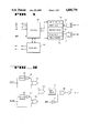
- FIG. 1 is a block diagram of the first-in first-out buffer memory of the present invention.
- FIG. 2 is a block diagram of the flag generator 34 of FIG. 1.
- FIG. 3 is a simplified circuit schematic for the delay circuit 46 of FIG. 2.
- FIG. 4 is a circuit diagram for the latch 44 of FIG. 2 and the time delay circuits associated therewith.
- the basic memory array 20 in this case a 64 ⁇ 9 memory array, is a dual port memory capable of being written to and read from simultaneously, whether synchronously or asynchronously.
- the data bits D0 through D8 are presented to the write multiplexor 24 and written to the memory as directed by the write pointer 22 and as controlled by the control logic 26.
- the input ready signal IR will go high, the new data being read thereinto when the input device connected to the FIFO buffer memory pulls the shift in signal SI high.
- the read multiplexer 28 reads the appropriate memory location as directed by the read pointer 30 under the control of the control logic 26.
- the output ready signal OR will go high, any time after which the output device connected to the FIFO buffer memory can cause data to be strobed therefrom by bringing the shift out signal SO high.
- the output ready signal OR will be held low indicating that fact, whereas when the memory is full, the input ready signal IR will be held low to similarly provide an indication thereof.
- a flag generator 34 which generates additional memory status flags, in this embodiment a half full flag HF and an almost full/empty flag AFE.
- the half full flag HF stays low whenever the memory has less than 32 bytes therein, and stays high if the memory has 32 or more bytes therein.
- the HF flag will be low if the memory contains zero to 31 bytes, and will be high if the memory contains 32 to 64 bytes.
- the almost full/empty flag AFE is used to indicate that the memory is approaching the full or empty condition, in the embodiment disclosed herein representing 56 or more bytes, or 8 or less bytes of information currently stored therein.
- the IR and OR signal each only enable and disable a single memory function, these flags need only be valid some known time after the previous similar function was initiated. Actually, in the embodiments disclosed, the IR and OR signals, respectively, go low following the SI and SO signals, respectively, to indicate that the same have been responded to, returning to their proper state when the SI or SO signal goes low again.
- the HF and AFE flags on the other hand, being intended to indicate memory status in the presence of asynchronous read and write operations, should be valid substantially continuously so that they can be monitored continuously, as their dependence on both asynchronous read and write operations would make it particularly inconvenient if a user of the FIFO buffer memory had to also consider the timing of the read and write operations to determine when these flags were valid. Accordingly, one of the primary purposes of the present invention is to provide additional flags such as the HF and AFE flags which are substantially continuously valid irrespective of the required flag generation times and the probable asynchronous nature of the read and write operations.
- FIG. 2 a block diagram of the flag generator 34 of FIG. 1 may be seen.
- This circuit has as its inputs, the read clock RLOAD and the inverse thereof, RLOAD, and the inverse of the write clock, LOAD, with the LOAD signal being generated within the circuit by inverter 36.
- RLOAD read clock
- LOAD write clock
- Generated within this circuit are the half full flag HF and the almost full/empty flag AFE, as well as a full flag FM1 and an empty flag EM1 which are used by the control 26 (FIG. 1) in the generation and/or inhibiting of the input ready flag IR and the output ready flag OR, respectively.
- the reset signal RST also available in this circuit is the reset signal RST, resetting various parts of the circuit upon command.
- decoder 42 is a random logic decoder whose decoded outputs merely follow the coded inputs thereto, though the reset signal is provided to the decoder to drive the output thereof to the reset condition to reduce the reset time thereof and to more quickly provide the appropriate output signals representing the reset condition to the input of the latch 44.
- the reset signal RST is coupled to the delay circuit 46 which, as shall subsequently be seen, is reflected in the delayed clock signal DCLK controlling latches 44 and 48, latch 44, as shall subsequently be seen, also having time delay circuits therein.
- the read counter 38 in the preferred embodiment is reset to 63, and the write counter 40 is reset to zero.
- the outputs of these two counters are coupled to a subtractor 50 which provides a multiple bit output to latch 48 representing the difference in the two counts. This difference is latched into latch 48 by one or more delayed clock signals DCLK after the output of the subtractor 50 has had sufficient time to settle.
- the output of the latch 48 in turn is decoded by decoder 42, with the decoded outputs FM1, EMIP, HF and AFE being latched into latch 44 containing its own time delay circuits, after the output of decoder 42 has had an opportunity to settle. Based on the foregoing, it may be seen that the outputs of the circuit of FIG.
- FIG. 3 a simplified circuit diagram of part of the delay circuit 46 of FIG. 2 may be seen.
- the LOAD signal is applied as one input of NAND gate 52 and is also passed through a delay circuit 54 and inverter 56 to provide the second input to NAND gate 52.
- the RLOAD signal is applied as one input to NAND gate 58 and is also passed through a delay circuit 60 and inverter 62 as the second input of the NAND gate 58.
- the delay circuits 54 and 60 are identical circuits of a type to be further described later.
- NAND gates 52 and 58 are coupled as the inputs to NAND gate 64, the output of which is passed through an additional time delay circuit 66 to provide one input to NOR gate 68.
- the other input to NOR gate 68 is the reset signal resulting in the inversion of the RST signal by inverter 70.
- the output of NOR gate 68 is inverted by inverter 72 to provide the delayed clock signal DCLK.
- the function of the circuit of FIG. 3 is to provide a delayed signal for clocking the latch 48 as soon as the output of subtractor 50 has had an opportunity to settle following a change in the read or write counters.
- the time delay circuit 66 has a delay substantially equal to the longest time delay for such settling (time delays for the settling after different changes will differ depending upon the specific change which is occurring) to assure that the difference count provided to the latch is valid before being latched into the latch.
- the time delays 54 and 60 define the width of the pulse DCLK clocking the latching. In particular, if both LOAD and RLOAD are low, at least one input to each of NAND gates 52 and 58 is low, making the outputs thereof high.
- the output of NAND gate 64 is a pulse initiated by the LOAD signal, going high and terminating a short period thereafter in accordance with the delay time of delay circuit 54. Both the leading edges and trailing edges of the pulse are delayed by the delay circuit 66, so that the DCLK signal will be a pulse having a pulse width determined by the delay period of delay circuit 54, and starting a given time period after the LOAD signal goes high as determined by the time delay of time delay circuit 66.
- the circuit connected to the RLOAD signal of course performs in a similar manner in response to the RLOAD signal going high, so that the identical time delayed clock pulse DCLK will be generated for either load or RLOAD going high.
- the details of the latch 44 and time delay circuits associated therewith may be seen.
- the actual circuit as opposed to a simplified circuit diagram is shown, both to provide specificity to a specific embodiment of the latch, and further, to provide circuit details exemplary of the techniques used in the time delay circuit 46.
- the delayed clock signal DCLK is coupled through a series of inverters 74 to provide one input to NOR gate 76.
- field effect devices 78 coupled as capacitors to provide increased capacitive loading on the output of each except the last of the six inverters.
- the chain of inverters with capacitive loading on the outputs thereof form an additional time delay so that the corresponding input to NOR gate 76 is a further delayed DCLK signal.
- the other input to the NOR gate 76 is the reset signal, inverted by inverter 80 from the RST signal applied thereto.
- This reset signal as applied to the input to NOR gate 76 is normally low, so that the output of the NOR gate is normally a delayed inverse of the DCLK signal.
- the output of inverter 84 will be the inverse of the delayed signal.
- the delayed DCLK signal on the output of inverter 82 is sufficiently delayed for the HF and the AFE signals to settle after any change thereof following the initiation of a read or write operation.
- This delayed DCLK signal on the output of inverter 82 then turns on field effect devices 86 and 88, with inverters 84 and 90 simultaneously cutting off field effect devices 92 and 94.
- the gates of field effect devices 86 and 88 will go low, turning the devices off, and at the same time the gates of field effect devices 92 and 94 will go high, turning the same on.
- the input to inverter 100 is the signal HF
- the output thereof is HF, which is maintained as the input to inverter 96.
- the combination of the two inverters 96 and 100 act as a toggle or latch to hold the output HF so long as field effect device 92 is maintained on.
- inverters 98 and 102 act as a latch to maintain the output signal AFE so long as field effect device 94 is maintained on.
- the delayed DCLK signal a pulse of very short duration, causes the latching of the new outputs for HF and AFE to provide the half full and almost full/empty flag outputs of the FIFO buffer memory.
- the DCLK signal is also coupled through inverters 104 and 110, with field effect devices 106 and 108 providing some short time delay, to the latch circuits for the signals FM1 and EM1P.
- the circuit comprising field effect devices 112 and 114 and inverters 116, 118, and 120 is the same as and functions the same as that provided by field effect devices 86 and 92 and inverters 84, 96 and 100, though of course inverting the FM1 signal and latching the same for the FM1 output upon the coupling of the delayed DCLK signal through inverters 122 and 124.
- field effect devices 126 and 128 and inverters 130, 132 and 134 function the same as field effect devices 112 and 114 and inverters 116, 120 and 118, though in this case the output is taken not from the output of inverter 132, but from the output of the inverter 134, so that the output EM1 is the non-inverted equivalent to input EMIP.
- the DCLK signal as delayed through inverters 104 and 110 by field effect devices 106 and 108 is further delayed through inverters 136 and 138 by field effect devices 140 and 142.
- the signal FM1 indicating a memory full condition, and the signal EM1 indicating a memory empty condition are signals used to generate or inhibit the input ready (IR) and output ready (OR) signals of the FIFO buffer memory within the control 26.
Abstract
Description
______________________________________
Memory Content     HF     AFE
______________________________________
0-8                0      1
 9-31              0      0
32-55              1      0
56-64              1      1
______________________________________
Claims (8)
Priority Applications (1)
| Application Number | Priority Date | Filing Date | Title |
|---|---|---|---|
| US07/207,249 US4888739A (en) | 1988-06-15 | 1988-06-15 | First-in first-out buffer memory with improved status flags |
Applications Claiming Priority (1)
| Application Number | Priority Date | Filing Date | Title |
|---|---|---|---|
| US07/207,249 US4888739A (en) | 1988-06-15 | 1988-06-15 | First-in first-out buffer memory with improved status flags |
Publications (1)
| Publication Number | Publication Date |
|---|---|
| US4888739A true US4888739A (en) | 1989-12-19 |
Family
ID=22769770
Family Applications (1)
| Application Number | Title | Priority Date | Filing Date |
|---|---|---|---|
| US07/207,249 Expired - Lifetime US4888739A (en) | 1988-06-15 | 1988-06-15 | First-in first-out buffer memory with improved status flags |
Country Status (1)
| Country | Link |
|---|---|
| US (1) | US4888739A (en) |
Cited By (56)
| Publication number | Priority date | Publication date | Assignee | Title |
|---|---|---|---|---|
| US5027330A (en) * | 1988-12-30 | 1991-06-25 | At&T Bell Laboratories | FIFO memory arrangement including a memory location fill indication |
| US5036489A (en) * | 1990-04-27 | 1991-07-30 | Codex Corp. | Compact expandable folded first-in-first-out queue |
| EP0481751A2 (en) * | 1990-10-18 | 1992-04-22 | STMicroelectronics, Inc. | Pipeline circuitry for allowing the comparison of the relative difference between two asynchronous pointers and a programmable value |
| EP0525874A2 (en) * | 1991-07-31 | 1993-02-03 | STMicroelectronics S.r.l. | Asynchronous access FIFO memory buffer with padding flag |
| US5193153A (en) * | 1988-12-30 | 1993-03-09 | Alcatel Cit | System for detecting overwriting of data in a buffer memory, particularly for a data switch |
| EP0564137A1 (en) * | 1992-03-31 | 1993-10-06 | STMicroelectronics, Inc. | Parallelized borrow look ahead subtractor |
| US5255238A (en) * | 1988-09-08 | 1993-10-19 | Hitachi, Ltd. | First-in first-out semiconductor memory device |
| US5262997A (en) * | 1991-11-25 | 1993-11-16 | Industrial Technology Research Institute | Extendable FIFO |
| US5267191A (en) * | 1989-04-03 | 1993-11-30 | Ncr Corporation | FIFO memory system |
| US5280584A (en) * | 1989-11-21 | 1994-01-18 | Deutsche Itt Industries Gmbh | Two-way data transfer apparatus |
| US5311475A (en) * | 1991-04-26 | 1994-05-10 | Quality Semiconductor Inc. | High speed full and empty flag generators for first-in first-out memory |
| US5323272A (en) * | 1992-07-01 | 1994-06-21 | Ampex Systems Corporation | Time delay control for serial digital video interface audio receiver buffer |
| US5325487A (en) * | 1990-08-14 | 1994-06-28 | Integrated Device Technology, Inc. | Shadow pipeline architecture in FIFO buffer |
| US5379399A (en) * | 1991-10-17 | 1995-01-03 | International Business Machines Corporation | FIFO memory controller for a digital video communications channel having a detector, comparator, and threshold select logic circuit |
| US5410723A (en) * | 1989-11-21 | 1995-04-25 | Deutsche Itt Industries Gmbh | Wavefront array processor for blocking the issuance of first handshake signal (req) by the presence of second handshake signal (ack) which indicates the readyness of the receiving cell |
| US5473756A (en) * | 1992-12-30 | 1995-12-05 | Intel Corporation | FIFO buffer with full/empty detection by comparing respective registers in read and write circular shift registers |
| US5490257A (en) * | 1992-02-24 | 1996-02-06 | Advanced Micro Devices, Inc. | RAM based FIFO memory half-full detection apparatus and method |
| US5502655A (en) * | 1989-03-31 | 1996-03-26 | Sgs-Thomson Microelectronics, Inc. | Difference comparison between two asynchronous pointers and a programmable value |
| US5519701A (en) * | 1995-03-29 | 1996-05-21 | International Business Machines Corporation | Architecture for high performance management of multiple circular FIFO storage means |
| US5615355A (en) * | 1992-10-22 | 1997-03-25 | Ampex Corporation | Method and apparatus for buffering a user application from the timing requirements of a DRAM |
| US5668767A (en) * | 1995-12-29 | 1997-09-16 | Cypress Semiconductor Corp. | Polled FIFO flags |
| US5682554A (en) * | 1993-01-15 | 1997-10-28 | Silicon Graphics, Inc. | Apparatus and method for handling data transfer between a general purpose computer and a cooperating processor |
| US5696940A (en) * | 1995-09-29 | 1997-12-09 | Intel Corporation | Apparatus and method for sharing first-in first-out memory space between two streams of data |
| US5809339A (en) * | 1995-12-06 | 1998-09-15 | Cypress Semiconductor Corp. | State machine design for generating half-full and half-empty flags in an asynchronous FIFO |
| US5844423A (en) * | 1995-12-14 | 1998-12-01 | Cypress Semiconductor Corporation | Half-full flag generator for synchronous FIFOs |
| US5850568A (en) * | 1995-12-22 | 1998-12-15 | Cypress Semiconductor Corporation | Circuit having plurality of carry/sum adders having read count, write count, and offset inputs to generate an output flag in response to FIFO fullness |
| US5852748A (en) * | 1995-12-29 | 1998-12-22 | Cypress Semiconductor Corp. | Programmable read-write word line equality signal generation for FIFOs |
| US5870340A (en) * | 1994-02-25 | 1999-02-09 | Kabushiki Kaisha Toshiba | Multiplexer |
| US5873089A (en) * | 1995-09-04 | 1999-02-16 | Hewlett-Packard Company | Data handling system with circular queue formed in paged memory |
| US5904732A (en) * | 1994-12-22 | 1999-05-18 | Sun Microsystems, Inc. | Dynamic priority switching of load and store buffers in superscalar processor |
| US5938739A (en) * | 1994-10-14 | 1999-08-17 | Compaq Computer Corporation | Memory controller including write posting queues, bus read control logic, and a data contents counter |
| US5955897A (en) * | 1996-03-13 | 1999-09-21 | Cypress Semiconductor Corp. | Signal generation decoder circuit and method |
| US5963056A (en) * | 1995-12-14 | 1999-10-05 | Cypress Semiconductor Corp. | Full and empty flag generator for synchronous FIFOs |
| US6016403A (en) * | 1995-12-06 | 2000-01-18 | Cypress Semiconductor Corp. | State machine design for generating empty and full flags in an asynchronous FIFO |
| US6067267A (en) * | 1998-08-12 | 2000-05-23 | Toshiba America Electronic Components, Inc. | Four-way interleaved FIFO architecture with look ahead conditional decoder for PCI applications |
| US6209047B1 (en) * | 1995-11-03 | 2001-03-27 | Samsung Electronics Co., Ltd. | RAM data transmitting apparatus and method using a FIFO memory with three fullness flags |
| US6389490B1 (en) * | 1999-10-07 | 2002-05-14 | Xilinx, Inc. | FIFO memory system and method with improved generation of empty and full control signals in one clock cycle using almost empty and almost full signals |
| US20020065665A1 (en) * | 2000-10-17 | 2002-05-30 | Hitachi, Ltd. | Digital data decompressing system and method |
| US6463000B2 (en) * | 2000-12-26 | 2002-10-08 | Samsung Electronics Co., Ltd. | First-in first-out memory device and method of generating flag signal in the same |
| US6473815B1 (en) * | 1999-10-12 | 2002-10-29 | At&T Corporation | Queue sharing |
| US6678759B2 (en) | 2001-07-26 | 2004-01-13 | Jsi Microelectronics, Inc. | Glitch suppression circuit and method |
| US20040019715A1 (en) * | 2001-02-06 | 2004-01-29 | Raphael Apfeldorfer | Multirate circular buffer and method of operating the same |
| US6745265B1 (en) | 2000-03-21 | 2004-06-01 | Agere Systems Inc. | Method and apparatus for generating status flags in a memory device |
| US6807589B2 (en) * | 2001-02-06 | 2004-10-19 | Nortel Networks S.A. | Multirate circular buffer and method of operating the same |
| US20060018177A1 (en) * | 2004-07-26 | 2006-01-26 | Integrated Device Technology, Inc. | Multiple counters to relieve flag restriction in a multi-queue first-in first-out memory system |
| US20060018176A1 (en) * | 2004-07-26 | 2006-01-26 | Integrated Device Technology, Inc. | Mark/re-read and mark/re-write operations in a multi-queue first-in first-out memory system |
| US20060020741A1 (en) * | 2004-07-26 | 2006-01-26 | Integrated Device Technology, Inc. | Synchronization of active flag and status bus flags in a multi-queue first-in first-out memory system |
| US6996640B1 (en) | 2001-08-07 | 2006-02-07 | Adaptec, Inc. | Method and system for asynchronously transferring data |
| US7227876B1 (en) | 2002-01-28 | 2007-06-05 | Pmc-Sierra, Inc. | FIFO buffer depth estimation for asynchronous gapped payloads |
| US20080049036A1 (en) * | 2006-08-24 | 2008-02-28 | Mediatek Inc. | Multimedia Playback System, FIFO Memory System, and Method for Storing Multimedia Data |
| US7392354B1 (en) | 2005-01-10 | 2008-06-24 | Integrated Device Technology, Inc. | Multi-queue FIFO memory devices that support a backed-off standard mode of operation and methods of operating same |
| US7447812B1 (en) | 2004-03-23 | 2008-11-04 | Integrated Device Technology, Inc. | Multi-queue FIFO memory devices that support flow-through of write and read counter updates using multi-port flag counter register files |
| US20100226442A1 (en) * | 2009-03-06 | 2010-09-09 | Himax Media Solutions, Inc. | Bit stream buffer controller and its method |
| US7805552B2 (en) | 2004-07-26 | 2010-09-28 | Integrated Device Technology, Inc. | Partial packet write and write data filtering in a multi-queue first-in first-out memory system |
| US8230174B2 (en) | 2004-07-26 | 2012-07-24 | Integrated Device Technology, Inc. | Multi-queue address generator for start and end addresses in a multi-queue first-in first-out memory system |
| CN113688074A (en) * | 2021-10-26 | 2021-11-23 | 浙江芯昇电子技术有限公司 | First-in first-out data processing device and data processing method |
Citations (1)
| Publication number | Priority date | Publication date | Assignee | Title |
|---|---|---|---|---|
| US4694426A (en) * | 1985-12-20 | 1987-09-15 | Ncr Corporation | Asynchronous FIFO status circuit |
-
1988
- 1988-06-15 US US07/207,249 patent/US4888739A/en not_active Expired - Lifetime
Patent Citations (1)
| Publication number | Priority date | Publication date | Assignee | Title |
|---|---|---|---|---|
| US4694426A (en) * | 1985-12-20 | 1987-09-15 | Ncr Corporation | Asynchronous FIFO status circuit |
Non-Patent Citations (4)
| Title |
|---|
| "FIFO-The Glue Holding Systems Together", by Ching-Lin Jiang and Michael Bolan, pp. 181-189, Computer Design Magazine, Jun. 1983. |
| Computer Design, Aug. 1, 1986, pp. 109 112, FIFO RAM Controller Tackles Deep Data Buffering , by Tom Pai. * |
| Computer Design, Aug. 1, 1986, pp. 109-112, "FIFO RAM Controller Tackles Deep Data Buffering", by Tom Pai. |
| FIFO The Glue Holding Systems Together , by Ching Lin Jiang and Michael Bolan, pp. 181 189, Computer Design Magazine, Jun. 1983. * |
Cited By (71)
| Publication number | Priority date | Publication date | Assignee | Title |
|---|---|---|---|---|
| US5426612A (en) * | 1988-09-08 | 1995-06-20 | Hitachi, Ltd. | First-in first-out semiconductor memory device |
| US5255238A (en) * | 1988-09-08 | 1993-10-19 | Hitachi, Ltd. | First-in first-out semiconductor memory device |
| US5027330A (en) * | 1988-12-30 | 1991-06-25 | At&T Bell Laboratories | FIFO memory arrangement including a memory location fill indication |
| US5193153A (en) * | 1988-12-30 | 1993-03-09 | Alcatel Cit | System for detecting overwriting of data in a buffer memory, particularly for a data switch |
| US5206817A (en) * | 1989-03-31 | 1993-04-27 | Sgs-Thomson Microelectronics, Inc. | Pipelined circuitry for allowing the comparison of the relative difference between two asynchronous pointers and a programmable value |
| US5502655A (en) * | 1989-03-31 | 1996-03-26 | Sgs-Thomson Microelectronics, Inc. | Difference comparison between two asynchronous pointers and a programmable value |
| US5267191A (en) * | 1989-04-03 | 1993-11-30 | Ncr Corporation | FIFO memory system |
| US5410723A (en) * | 1989-11-21 | 1995-04-25 | Deutsche Itt Industries Gmbh | Wavefront array processor for blocking the issuance of first handshake signal (req) by the presence of second handshake signal (ack) which indicates the readyness of the receiving cell |
| US5280584A (en) * | 1989-11-21 | 1994-01-18 | Deutsche Itt Industries Gmbh | Two-way data transfer apparatus |
| US5036489A (en) * | 1990-04-27 | 1991-07-30 | Codex Corp. | Compact expandable folded first-in-first-out queue |
| US5471583A (en) * | 1990-08-14 | 1995-11-28 | Integrated Device Technology, Inc. | FIFO buffer having write counter for generating empty flag value to be compared with read pointer value to indicate the buffer is full |
| US5325487A (en) * | 1990-08-14 | 1994-06-28 | Integrated Device Technology, Inc. | Shadow pipeline architecture in FIFO buffer |
| EP0481751A3 (en) * | 1990-10-18 | 1993-02-24 | Sgs-Thomson Microelectronics, Inc. | Pipeline circuitry for allowing the comparison of the relative difference between two asynchronous pointers and a programmable value |
| EP0481751A2 (en) * | 1990-10-18 | 1992-04-22 | STMicroelectronics, Inc. | Pipeline circuitry for allowing the comparison of the relative difference between two asynchronous pointers and a programmable value |
| US5311475A (en) * | 1991-04-26 | 1994-05-10 | Quality Semiconductor Inc. | High speed full and empty flag generators for first-in first-out memory |
| EP0525874A3 (en) * | 1991-07-31 | 1994-03-16 | Sgs Thomson Microelectronics | |
| EP0525874A2 (en) * | 1991-07-31 | 1993-02-03 | STMicroelectronics S.r.l. | Asynchronous access FIFO memory buffer with padding flag |
| US5379399A (en) * | 1991-10-17 | 1995-01-03 | International Business Machines Corporation | FIFO memory controller for a digital video communications channel having a detector, comparator, and threshold select logic circuit |
| US5262997A (en) * | 1991-11-25 | 1993-11-16 | Industrial Technology Research Institute | Extendable FIFO |
| US5490257A (en) * | 1992-02-24 | 1996-02-06 | Advanced Micro Devices, Inc. | RAM based FIFO memory half-full detection apparatus and method |
| US5386377A (en) * | 1992-03-31 | 1995-01-31 | Sgs-Thomson Microelectronics, Inc. | Parallelized borrow look ahead subtractor |
| EP0564137A1 (en) * | 1992-03-31 | 1993-10-06 | STMicroelectronics, Inc. | Parallelized borrow look ahead subtractor |
| US5323272A (en) * | 1992-07-01 | 1994-06-21 | Ampex Systems Corporation | Time delay control for serial digital video interface audio receiver buffer |
| US5615355A (en) * | 1992-10-22 | 1997-03-25 | Ampex Corporation | Method and apparatus for buffering a user application from the timing requirements of a DRAM |
| US5473756A (en) * | 1992-12-30 | 1995-12-05 | Intel Corporation | FIFO buffer with full/empty detection by comparing respective registers in read and write circular shift registers |
| US5682554A (en) * | 1993-01-15 | 1997-10-28 | Silicon Graphics, Inc. | Apparatus and method for handling data transfer between a general purpose computer and a cooperating processor |
| US5870340A (en) * | 1994-02-25 | 1999-02-09 | Kabushiki Kaisha Toshiba | Multiplexer |
| US5938739A (en) * | 1994-10-14 | 1999-08-17 | Compaq Computer Corporation | Memory controller including write posting queues, bus read control logic, and a data contents counter |
| US5904732A (en) * | 1994-12-22 | 1999-05-18 | Sun Microsystems, Inc. | Dynamic priority switching of load and store buffers in superscalar processor |
| US5519701A (en) * | 1995-03-29 | 1996-05-21 | International Business Machines Corporation | Architecture for high performance management of multiple circular FIFO storage means |
| US5873089A (en) * | 1995-09-04 | 1999-02-16 | Hewlett-Packard Company | Data handling system with circular queue formed in paged memory |
| US5696940A (en) * | 1995-09-29 | 1997-12-09 | Intel Corporation | Apparatus and method for sharing first-in first-out memory space between two streams of data |
| US6209047B1 (en) * | 1995-11-03 | 2001-03-27 | Samsung Electronics Co., Ltd. | RAM data transmitting apparatus and method using a FIFO memory with three fullness flags |
| US5991834A (en) * | 1995-12-06 | 1999-11-23 | Cypress Semiconductor Corp. | State machine design for generating half-full and half-empty flags in an asynchronous FIFO |
| US6016403A (en) * | 1995-12-06 | 2000-01-18 | Cypress Semiconductor Corp. | State machine design for generating empty and full flags in an asynchronous FIFO |
| US5809339A (en) * | 1995-12-06 | 1998-09-15 | Cypress Semiconductor Corp. | State machine design for generating half-full and half-empty flags in an asynchronous FIFO |
| US5844423A (en) * | 1995-12-14 | 1998-12-01 | Cypress Semiconductor Corporation | Half-full flag generator for synchronous FIFOs |
| US5963056A (en) * | 1995-12-14 | 1999-10-05 | Cypress Semiconductor Corp. | Full and empty flag generator for synchronous FIFOs |
| US5994920A (en) * | 1995-12-14 | 1999-11-30 | Cypress Semiconductor Corp. | Half-full flag generator for synchronous FIFOs |
| US6070203A (en) * | 1995-12-22 | 2000-05-30 | Cypress Semiconductor Corp. | Circuit for generating almost full and almost empty flags in response to sum and carry outputs in asynchronous and synchronous FIFOS |
| US5850568A (en) * | 1995-12-22 | 1998-12-15 | Cypress Semiconductor Corporation | Circuit having plurality of carry/sum adders having read count, write count, and offset inputs to generate an output flag in response to FIFO fullness |
| US5668767A (en) * | 1995-12-29 | 1997-09-16 | Cypress Semiconductor Corp. | Polled FIFO flags |
| US5852748A (en) * | 1995-12-29 | 1998-12-22 | Cypress Semiconductor Corp. | Programmable read-write word line equality signal generation for FIFOs |
| US5955897A (en) * | 1996-03-13 | 1999-09-21 | Cypress Semiconductor Corp. | Signal generation decoder circuit and method |
| US6067267A (en) * | 1998-08-12 | 2000-05-23 | Toshiba America Electronic Components, Inc. | Four-way interleaved FIFO architecture with look ahead conditional decoder for PCI applications |
| US6389490B1 (en) * | 1999-10-07 | 2002-05-14 | Xilinx, Inc. | FIFO memory system and method with improved generation of empty and full control signals in one clock cycle using almost empty and almost full signals |
| US6401148B1 (en) | 1999-10-07 | 2002-06-04 | Xilinx, Inc. | FIFO memory system and method with improved determination of amount of data stored using a binary read address synchronized to a write clock |
| US6434642B1 (en) | 1999-10-07 | 2002-08-13 | Xilinx, Inc. | FIFO memory system and method with improved determination of full and empty conditions and amount of data stored |
| US6473815B1 (en) * | 1999-10-12 | 2002-10-29 | At&T Corporation | Queue sharing |
| US6745265B1 (en) | 2000-03-21 | 2004-06-01 | Agere Systems Inc. | Method and apparatus for generating status flags in a memory device |
| US20020065665A1 (en) * | 2000-10-17 | 2002-05-30 | Hitachi, Ltd. | Digital data decompressing system and method |
| US6463000B2 (en) * | 2000-12-26 | 2002-10-08 | Samsung Electronics Co., Ltd. | First-in first-out memory device and method of generating flag signal in the same |
| US6807589B2 (en) * | 2001-02-06 | 2004-10-19 | Nortel Networks S.A. | Multirate circular buffer and method of operating the same |
| US20040019715A1 (en) * | 2001-02-06 | 2004-01-29 | Raphael Apfeldorfer | Multirate circular buffer and method of operating the same |
| US6678759B2 (en) | 2001-07-26 | 2004-01-13 | Jsi Microelectronics, Inc. | Glitch suppression circuit and method |
| US6996640B1 (en) | 2001-08-07 | 2006-02-07 | Adaptec, Inc. | Method and system for asynchronously transferring data |
| US7227876B1 (en) | 2002-01-28 | 2007-06-05 | Pmc-Sierra, Inc. | FIFO buffer depth estimation for asynchronous gapped payloads |
| US7447812B1 (en) | 2004-03-23 | 2008-11-04 | Integrated Device Technology, Inc. | Multi-queue FIFO memory devices that support flow-through of write and read counter updates using multi-port flag counter register files |
| US7257687B2 (en) * | 2004-07-26 | 2007-08-14 | Integrated Device Technology, Inc. | Synchronization of active flag and status bus flags in a multi-queue first-in first-out memory system |
| US20060020741A1 (en) * | 2004-07-26 | 2006-01-26 | Integrated Device Technology, Inc. | Synchronization of active flag and status bus flags in a multi-queue first-in first-out memory system |
| US20060018176A1 (en) * | 2004-07-26 | 2006-01-26 | Integrated Device Technology, Inc. | Mark/re-read and mark/re-write operations in a multi-queue first-in first-out memory system |
| US20060018177A1 (en) * | 2004-07-26 | 2006-01-26 | Integrated Device Technology, Inc. | Multiple counters to relieve flag restriction in a multi-queue first-in first-out memory system |
| US7523232B2 (en) | 2004-07-26 | 2009-04-21 | Integrated Device Technology, Inc. | Mark/re-read and mark/re-write operations in a multi-queue first-in first-out memory system |
| US7805552B2 (en) | 2004-07-26 | 2010-09-28 | Integrated Device Technology, Inc. | Partial packet write and write data filtering in a multi-queue first-in first-out memory system |
| US7870310B2 (en) | 2004-07-26 | 2011-01-11 | Integrated Device Technology, Inc. | Multiple counters to relieve flag restriction in a multi-queue first-in first-out memory system |
| US8230174B2 (en) | 2004-07-26 | 2012-07-24 | Integrated Device Technology, Inc. | Multi-queue address generator for start and end addresses in a multi-queue first-in first-out memory system |
| US7392354B1 (en) | 2005-01-10 | 2008-06-24 | Integrated Device Technology, Inc. | Multi-queue FIFO memory devices that support a backed-off standard mode of operation and methods of operating same |
| US20080049036A1 (en) * | 2006-08-24 | 2008-02-28 | Mediatek Inc. | Multimedia Playback System, FIFO Memory System, and Method for Storing Multimedia Data |
| US20100226442A1 (en) * | 2009-03-06 | 2010-09-09 | Himax Media Solutions, Inc. | Bit stream buffer controller and its method |
| US8194755B2 (en) * | 2009-03-06 | 2012-06-05 | Himax Media Solutions, Inc. | Bit stream buffer controller and its method |
| CN113688074A (en) * | 2021-10-26 | 2021-11-23 | 浙江芯昇电子技术有限公司 | First-in first-out data processing device and data processing method |
Similar Documents
| Publication | Publication Date | Title |
|---|---|---|
| US4888739A (en) | First-in first-out buffer memory with improved status flags | |
| US4864543A (en) | First-in, first-out memory with counter address pointers for generating multiple memory status flags | |
| US5365485A (en) | Fifo with fast retransmit mode | |
| US4839866A (en) | Cascadable first-in, first-out memory | |
| US4750149A (en) | Programmable FIFO buffer | |
| US4888741A (en) | Memory with cache register interface structure | |
| US5524270A (en) | System for transferring data between asynchronous data buses with a data buffer interposed in between the buses for synchronization of devices timed by different clocks | |
| US4873667A (en) | FIFO buffer controller | |
| US5274600A (en) | First-in first-out memory | |
| US9218860B2 (en) | Multiple data rate memory with read timing information | |
| US5426380A (en) | High speed processing flip-flop | |
| US4825416A (en) | Integrated electronic memory circuit with internal timing and operable in both latch-based and register-based systems | |
| US4815039A (en) | Fast real-time arbiter | |
| US5206817A (en) | Pipelined circuitry for allowing the comparison of the relative difference between two asynchronous pointers and a programmable value | |
| KR100275182B1 (en) | Sequential memmory | |
| US5021994A (en) | Look-ahead flag generator | |
| US20020080672A1 (en) | First-in first-out memory device and method of generating flag signal in the same | |
| US4922457A (en) | Serial access memory system provided with improved cascade buffer circuit | |
| US5033066A (en) | Event tagging time delay | |
| KR0137771B1 (en) | Fifo with almost full/almost empty flag | |
| US6286072B1 (en) | System and method for synchronizing data communication between asynchronous buses | |
| US6289065B1 (en) | FIFO status indicator | |
| US4789959A (en) | Delay circuit for a real time clock | |
| US5249154A (en) | Data access controller and method | |
| US5255242A (en) | Sequential memory |
Legal Events
| Date | Code | Title | Description |
|---|---|---|---|
| AS | Assignment |
Owner name: CYPRESS SEMICONDUCTOR CORPORATION, 3901 NORTH FIRS Free format text: ASSIGNMENT OF ASSIGNORS INTEREST.;ASSIGNORS:FREDERICK, BRUCE;KESWICK, PAUL;REEL/FRAME:004921/0974 Effective date: 19880621 |
|
| STCF | Information on status: patent grant |
Free format text: PATENTED CASE |
|
| FEPP | Fee payment procedure |
Free format text: PAYOR NUMBER ASSIGNED (ORIGINAL EVENT CODE: ASPN); ENTITY STATUS OF PATENT OWNER: LARGE ENTITY |
|
| FPAY | Fee payment |
Year of fee payment: 4 |
|
| FPAY | Fee payment |
Year of fee payment: 8 |
|
| REMI | Maintenance fee reminder mailed | ||
| FPAY | Fee payment |
Year of fee payment: 12 |
|
| SULP | Surcharge for late payment |
Year of fee payment: 11 |
|
| FEPP | Fee payment procedure |
Free format text: PAYOR NUMBER ASSIGNED (ORIGINAL EVENT CODE: ASPN); ENTITY STATUS OF PATENT OWNER: LARGE ENTITY Free format text: PAYER NUMBER DE-ASSIGNED (ORIGINAL EVENT CODE: RMPN); ENTITY STATUS OF PATENT OWNER: LARGE ENTITY |