US4887353A - Conduction cooled module connector system and method of making - Google Patents
Conduction cooled module connector system and method of making Download PDFInfo
- Publication number
- US4887353A US4887353A US06/729,432 US72943285A US4887353A US 4887353 A US4887353 A US 4887353A US 72943285 A US72943285 A US 72943285A US 4887353 A US4887353 A US 4887353A
- Authority
- US
- United States
- Prior art keywords
- electrical
- electrical connectors
- daughter cards
- connectors
- connector
- Prior art date
- Legal status (The legal status is an assumption and is not a legal conclusion. Google has not performed a legal analysis and makes no representation as to the accuracy of the status listed.)
- Expired - Lifetime
Links
Images


Classifications
-
- H—ELECTRICITY
- H01—ELECTRIC ELEMENTS
- H01R—ELECTRICALLY-CONDUCTIVE CONNECTIONS; STRUCTURAL ASSOCIATIONS OF A PLURALITY OF MUTUALLY-INSULATED ELECTRICAL CONNECTING ELEMENTS; COUPLING DEVICES; CURRENT COLLECTORS
- H01R12/00—Structural associations of a plurality of mutually-insulated electrical connecting elements, specially adapted for printed circuits, e.g. printed circuit boards [PCB], flat or ribbon cables, or like generally planar structures, e.g. terminal strips, terminal blocks; Coupling devices specially adapted for printed circuits, flat or ribbon cables, or like generally planar structures; Terminals specially adapted for contact with, or insertion into, printed circuits, flat or ribbon cables, or like generally planar structures
- H01R12/70—Coupling devices
- H01R12/71—Coupling devices for rigid printing circuits or like structures
- H01R12/72—Coupling devices for rigid printing circuits or like structures coupling with the edge of the rigid printed circuits or like structures
- H01R12/722—Coupling devices for rigid printing circuits or like structures coupling with the edge of the rigid printed circuits or like structures coupling devices mounted on the edge of the printed circuits
- H01R12/725—Coupling devices for rigid printing circuits or like structures coupling with the edge of the rigid printed circuits or like structures coupling devices mounted on the edge of the printed circuits containing contact members presenting a contact carrying strip, e.g. edge-like strip
-
- Y—GENERAL TAGGING OF NEW TECHNOLOGICAL DEVELOPMENTS; GENERAL TAGGING OF CROSS-SECTIONAL TECHNOLOGIES SPANNING OVER SEVERAL SECTIONS OF THE IPC; TECHNICAL SUBJECTS COVERED BY FORMER USPC CROSS-REFERENCE ART COLLECTIONS [XRACs] AND DIGESTS
- Y10—TECHNICAL SUBJECTS COVERED BY FORMER USPC
- Y10T—TECHNICAL SUBJECTS COVERED BY FORMER US CLASSIFICATION
- Y10T29/00—Metal working
- Y10T29/49—Method of mechanical manufacture
- Y10T29/49002—Electrical device making
- Y10T29/49117—Conductor or circuit manufacturing
- Y10T29/49124—On flat or curved insulated base, e.g., printed circuit, etc.
- Y10T29/49126—Assembling bases
Definitions
- the invention disclosed herein pertains to card edge connectors and a heat sink to conduct heat away from a pair of parallel circuit cards terminated in separate card edge connectors and which are thereafter joined to form a single connector.
- Contemporary systems include a heat sink which is mounted between two circuit cards prior to the circuit cards being mounted on card edge connectors. Upon testing the connectors and finding defective contact members, the entire assembly must be carefully disassembled to replace such defective members.
- the present invention discloses a card edge connector system including a conduction type heat sink sandwiched between a pair of circuit cards. More particularly, the invention teaches a method of first mounting daughter cards on receptacle units, testing the electrical integrity therebetween, replacing defective contact elements as required, securing the two units together with a heat sink between the cards and mounting the two secured units onto a pin header mounted on a circuit board.
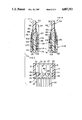
- FIG. 1 is a perspective view of the connector system of the present invention prior to being assembled
- FIG. 2 is a cross-sectional end view showing the first stage of assembling the connector system
- FIG. 3 is a perspective view of the assembled connector system
- FIG. 4 is a cross-sectional end view of the assembled connector system.
- the major components of the connector system seen in FIG. 1, are indicated generally by reference numeral 10 and include pin header 12 and two receptacle units 14.
- Pin header 12 includes an insulating housing 16 and contact pins 18.
- the housing is preferably molded from a polyphenylene sulfide resin sold under the trade name RYTON by the Phillips Chemical Company.
- An upwardly open cavity 20 is provided in the housing.
- Polarizing slots 22 are located in opposing end walls of the cavity 20.
- a transverse wall 24 is located in and midway between the ends of the cavity 20 and includes a keying opening 26. This wall 24 is attached to and extends between side walls 28 and 30. The surface of this transverse wall 24 is below the top surface of the housing.
- Two openings, indicated by reference numeral 32, are provided in housing 16, one on each side of cavity 20 and are adjacent side wall 28.
- FIG. 2 A transverse cross sectional view of pin header 12 is provided in FIG. 2.
- rows of contact pin receiving passages 34 extend from the floor 36 of cavity 20 down through housing 16 opening out on the downwardly facing surface 38.
- Each passage 34 includes large section 40 opening out at floor 36 and a small section 42, in communication with large section 40, extending downwardly therefrom and opening out at downwardly facing surface 38.
- Sections 40, 42 meet on one or the other side of a center-line (not shown) thru sections 40 in a predetermined pattern dictated by the density of contact pins 18 and holes 52 on circuit board 54.
- a center-line not shown
- the two small sections 42 on the right hand side of pin header 12 are to the right of center and the two small sections 42 on the left hand side are to the left of center.
- the reverse pattern holds; i.e., the two small sections 42 on the right hand side of pin header 12 are to the left of center and the two small sections 42 on the left hand side are to the right of center.
- the pattern of the two transverse rows described above repeats from one end of pin header 12 to the other end.
- FIG. 2 shows the general structure.
- Each pin 18 includes a square post 44 which extends up into cavity 20, an intermediate section 46 positioned in large section 40, a retaining section 48 positioned in small section 42 and a depending lead 50.
- These leads 50 are soldered into holes 52 in mother board 54 (FIG. 1).
- they could be of other configurations; e.g., a frictional fit utilizing a compliant section.
- Receptacle units 14 are shown isometrically in FIG. 1 and sectioned in FIGS. 2 and 4. While the two units 14 have common structure, there are differences: accordingly, the units 14 are distinguished by adding reference letters "L" for the left hand unit 14 and "R" for the right hand unit 14.
- Both units 14 include housing 56 (also distinguished by the letters "L” and "R”).
- the housing 56 preferably molded from polyphenylene sulfide resin, are formed to provide a longitudinally elongated upper half or portion 58 and a lower portion 60 of lesser length.
- the differing lengths define overhanging end portions 62.
- the length and depth of the lower portions 60 is equal to the length and depth of cavity 20 in pin header 12.
- the length of the upper sections 58 is equal to the length of pin header 12.
- the upwardly facing surface 63 on housings 56 include three, spaced apart areas 64 and two intervening, downwardly displaced areas 66. Each of the three areas 64 support an upwardly projecting ear 68. Holes 70 are provided in each ear 68 and the upwardly facing surface 72 thereof is flat. The ears 68 on housing 56-R are on that housing's inward side 74. The ears 68 on housing 56-L are on that housings's inward side 76. The inward sides 74 and 76 are seen more clearly in FIG. 2. These sides 74,76 abut when the units 14 are secured together as shown in FIG. 4.
- a downwardly opened, transverse notch 78 is provided in each lower portion 60 midway between the two ends. Further, on housing 56-L, the end walls 80 of lower portion 60 are recessed or stepped to define a short wall segment 82 on the outward side 84. The size of these segments 82 are such as to fit into slots 22 in pin header 12.
- Each receptacle unit 14 is loaded with two rows of spaced apart, contact elements 86 shown in FIGS. 2 and 4.
- Elements 86 include a cantilever spring arm 88 at the upper end with a convex surface 90 for being soldered to conductive traces 92 on dauaghter card 94.
- a box style receptacle 96 is provided on the lower end of element 86 and retention section 98 is positioned between receptacle 96 and arm 88.
- Contact-receiving passageway 100 in units 14 which receive elements 86 include an upper section 102 and a lower section 104 which is offset horizontally in relation to upper section 102. The offset is towards the longitudinal center line of units 14 and provides downwardly facing shoulder 106 and upwardly facing shoulder 108. These shoulders 106,108, in cooperation with the structure of element 86, retain element 86 in the contact-receiving passageway 100.
- the two rows of elements 86 are positioned in each unit 14 so that convex surfaces 90 face each other as shown.
- the system of the present invention is assembled by first loading contact pins 18 into pin header 12 and receptacle elements 86 into units 14.
- the header 12 and units 14 at this stage are as shown in FIG. 1.
- Pin header 12 is mounted onto printed circuit board 54 by inserting and soldering leads 50 into holes 52.
- daughter cards 94 are positioned on units 14 so that the ends and middle sections of lower edges 110 (FIG. 1) rest on flat, spaced apart areas 64 on upwardly facing surfaces 63 and holes 112 in cards 94 are in alignment with holes 70 in ears 68.
- the sections of the edges 110 having traces 92 are inserted between the two rows of cantilever arms 88 on elements 86 with the convex surfaces 90 bearing against respective traces 92.
- Convex surfaces 90 are next soldered to traces 92 to form the subassembly (Unit 14 plus card 94), indicated generally by reference numeral 114 in FIG. 2.
- the subassemblies 114 are then tested to insure electrical integrity. In the event a failure is present, it is a simple matter to replace defective elements 86 or cards 94.
- the two subassemblies 114L, 114R are bolted together with heat sink 116 therebetween as shown in FIGS. 3 and 4.
- Bolts 118 (FIGS. 3) pass through holes 112 in the cards 94 and holes 70 in ears 68.
- Heat sink 116 rests on flat surfaces 72 of ears 68 as shown in FIG. 4 and is held in place between the bolted together cards 94.
- the surface area of cards 94 which abut heat sink 116 is devoid of traces 92; such traces being diverted to opposing surfaces by means of vias (not shown) located near card edges 110. As is well known in the art, this arrangement permits a higher concentration of electronic packages (not shown) on such opposing surfaces.
- the two bolted together subassemblies 114L, 114R form module assembly 120 as shown in FIGS. 3 and 4.
- Module assembly 120 is now ready for placing into pin header 12 to complete the system assembly.
- the short wall segments 82 on each end of unit 14-L and slots 22 in pin header 12 provides proper orientation so that assembly 120 cannot be incorrectly inserted.
- posts 44 on contact pins 18 enter receptacles 96 on elements 86 in units 14-L, 14-R to electrically interconnect traces 92 on cards 94 with plated-through holes 52 in board 54 and hence to traces (not shown) on the board 54.
- the overhanging end portions 62 rest on upper surface 122, FIG. 3.
- the upper walls 124 defining notches 78 rest on transverse wall 24.
- bolts can be mounted in units 14-L, 14-R and openings 32 and 26 provided with threads to receive the bolts.
- the heat sink 116 are user designed. Materials commonly used to make such sinks include aluminum, copper and copper-invar-copper.
Abstract
A connector system incorporating a heat sink positioned between a pair of circuit cards terminated in a pair of joined receptacle units. A method is disclosed of connecting a daughter card to a receptacle unit, testing that subassembly, and then securing two such subassemblies together with a heat sink between the two cards to form an assembly to be mounted on a pin header mounted on a circuit board.
Description
1. Field of the Invention
The invention disclosed herein pertains to card edge connectors and a heat sink to conduct heat away from a pair of parallel circuit cards terminated in separate card edge connectors and which are thereafter joined to form a single connector.
2. Prior Art
Contemporary systems include a heat sink which is mounted between two circuit cards prior to the circuit cards being mounted on card edge connectors. Upon testing the connectors and finding defective contact members, the entire assembly must be carefully disassembled to replace such defective members.
The present invention discloses a card edge connector system including a conduction type heat sink sandwiched between a pair of circuit cards. More particularly, the invention teaches a method of first mounting daughter cards on receptacle units, testing the electrical integrity therebetween, replacing defective contact elements as required, securing the two units together with a heat sink between the cards and mounting the two secured units onto a pin header mounted on a circuit board.
FIG. 1 is a perspective view of the connector system of the present invention prior to being assembled;
FIG. 2 is a cross-sectional end view showing the first stage of assembling the connector system;
FIG. 3 is a perspective view of the assembled connector system; and
FIG. 4 is a cross-sectional end view of the assembled connector system.
The major components of the connector system seen in FIG. 1, are indicated generally by reference numeral 10 and include pin header 12 and two receptacle units 14.
A transverse cross sectional view of pin header 12 is provided in FIG. 2. There it can be seen that rows of contact pin receiving passages 34 extend from the floor 36 of cavity 20 down through housing 16 opening out on the downwardly facing surface 38. Each passage 34 includes large section 40 opening out at floor 36 and a small section 42, in communication with large section 40, extending downwardly therefrom and opening out at downwardly facing surface 38. Sections 40, 42 meet on one or the other side of a center-line (not shown) thru sections 40 in a predetermined pattern dictated by the density of contact pins 18 and holes 52 on circuit board 54. As shown in the transverse row of passages 34 in FIG. 2, the two small sections 42 on the right hand side of pin header 12 are to the right of center and the two small sections 42 on the left hand side are to the left of center. Not shown but discernible from leads 50 on the contact pins 18 in the transverse row behind the row shown, the reverse pattern holds; i.e., the two small sections 42 on the right hand side of pin header 12 are to the left of center and the two small sections 42 on the left hand side are to the right of center. The pattern of the two transverse rows described above repeats from one end of pin header 12 to the other end.
With regard to contact pins 18, FIG. 2 shows the general structure. Each pin 18 includes a square post 44 which extends up into cavity 20, an intermediate section 46 positioned in large section 40, a retaining section 48 positioned in small section 42 and a depending lead 50. These leads 50 are soldered into holes 52 in mother board 54 (FIG. 1). However, they could be of other configurations; e.g., a frictional fit utilizing a compliant section.
Both units 14 include housing 56 (also distinguished by the letters "L" and "R"). The housing 56, preferably molded from polyphenylene sulfide resin, are formed to provide a longitudinally elongated upper half or portion 58 and a lower portion 60 of lesser length. The differing lengths define overhanging end portions 62. The length and depth of the lower portions 60 is equal to the length and depth of cavity 20 in pin header 12. Preferably, the length of the upper sections 58 is equal to the length of pin header 12.
The upwardly facing surface 63 on housings 56 include three, spaced apart areas 64 and two intervening, downwardly displaced areas 66. Each of the three areas 64 support an upwardly projecting ear 68. Holes 70 are provided in each ear 68 and the upwardly facing surface 72 thereof is flat. The ears 68 on housing 56-R are on that housing's inward side 74. The ears 68 on housing 56-L are on that housings's inward side 76. The inward sides 74 and 76 are seen more clearly in FIG. 2. These sides 74,76 abut when the units 14 are secured together as shown in FIG. 4.
As seen in FIG. 1, a downwardly opened, transverse notch 78 is provided in each lower portion 60 midway between the two ends. Further, on housing 56-L, the end walls 80 of lower portion 60 are recessed or stepped to define a short wall segment 82 on the outward side 84. The size of these segments 82 are such as to fit into slots 22 in pin header 12.
Not shown are depending studs on the lower surfaces of overhanging end portions 62 on unit 14-R and in notch 78 of unit 14-L. These studs are located so as to enter openings 32 and 26 respectively.
Each receptacle unit 14 is loaded with two rows of spaced apart, contact elements 86 shown in FIGS. 2 and 4. Elements 86 include a cantilever spring arm 88 at the upper end with a convex surface 90 for being soldered to conductive traces 92 on dauaghter card 94. A box style receptacle 96 is provided on the lower end of element 86 and retention section 98 is positioned between receptacle 96 and arm 88.
Contact-receiving passageway 100 in units 14 which receive elements 86 include an upper section 102 and a lower section 104 which is offset horizontally in relation to upper section 102. The offset is towards the longitudinal center line of units 14 and provides downwardly facing shoulder 106 and upwardly facing shoulder 108. These shoulders 106,108, in cooperation with the structure of element 86, retain element 86 in the contact-receiving passageway 100.
Contact-receiving passageway 100 open out on both upper surface 63 and lower surface 109 of units 14.
The two rows of elements 86 are positioned in each unit 14 so that convex surfaces 90 face each other as shown.
The system of the present invention is assembled by first loading contact pins 18 into pin header 12 and receptacle elements 86 into units 14. The header 12 and units 14 at this stage are as shown in FIG. 1. Pin header 12 is mounted onto printed circuit board 54 by inserting and soldering leads 50 into holes 52. Next, daughter cards 94 are positioned on units 14 so that the ends and middle sections of lower edges 110 (FIG. 1) rest on flat, spaced apart areas 64 on upwardly facing surfaces 63 and holes 112 in cards 94 are in alignment with holes 70 in ears 68. Concurrently, the sections of the edges 110 having traces 92 are inserted between the two rows of cantilever arms 88 on elements 86 with the convex surfaces 90 bearing against respective traces 92. Convex surfaces 90 are next soldered to traces 92 to form the subassembly (Unit 14 plus card 94), indicated generally by reference numeral 114 in FIG. 2. The subassemblies 114 are then tested to insure electrical integrity. In the event a failure is present, it is a simple matter to replace defective elements 86 or cards 94.
After testing and any required repairing, the two subassemblies 114L, 114R are bolted together with heat sink 116 therebetween as shown in FIGS. 3 and 4. Bolts 118 (FIGS. 3) pass through holes 112 in the cards 94 and holes 70 in ears 68. Heat sink 116 rests on flat surfaces 72 of ears 68 as shown in FIG. 4 and is held in place between the bolted together cards 94. The surface area of cards 94 which abut heat sink 116 is devoid of traces 92; such traces being diverted to opposing surfaces by means of vias (not shown) located near card edges 110. As is well known in the art, this arrangement permits a higher concentration of electronic packages (not shown) on such opposing surfaces. The two bolted together subassemblies 114L, 114R form module assembly 120 as shown in FIGS. 3 and 4.
The heat sink 116 are user designed. Materials commonly used to make such sinks include aluminum, copper and copper-invar-copper.
Claims (6)
1. A method of forming connector assemblies and connecting them to a printed circuit board, comprising the steps of:
a. electrically connecting electrical contacts of first and second electrical connectors to respective conductive traces on first and second daughter cards thereby forming subassemblies;
b. testing the subassemblies to determine if electrical contacts or daughter cards should be replaced;
c. securing the first and second connectors together with a heat sink member disposed between the daughter cards; and
d. electrically connecting the first and second electrical connectors with a third electrical connector electrically connected to the printed circuit board.
2. The method of claim 1 further including the step of orientating the first and second electrical connectors relative to the third electrical connector with respect to cooperating polarizing means on the three electrical connectors.
3. An electrical connection assembly connecting daughter cards to a printed circuit board, comprising:
a. first and second electrical connectors having electrical contact members secured therein, said electrical contact members having first contact sections electrically connected to conductive traces on the daughter cards and second contact sections;
b. securing means provided by said first and second electrical connectors and the daughter cards securing said first and second electrical connectors and the daughter cards together, said securing means on said first and second electrical connectors engaging each other thereby spacing the daughter cards from each other and providing a space therebetween;
c. heat sink means disposed in said space between the daughter cards and secured therein by said securing means; and
d. a third connector electrically connected to the printed circuit board and having electrical contact means that electrically connect with the second contact sections of said first and second electrical connectors when they mate with said third connector.
4. The electrical connection assembly of claim 3 wherein the first and second electrical connectors include rear surfaces adapted for conformably engaging each other when said first and second electrical connectors are secured together.
5. The electrical connection assembly of claim 3 further including cooperating polarizing means on one of said first and second electrical connectors and on said third electrical connector.
6. The electrical connection assembly of claim 3 wherein the securing means include upwardly extending ears on each of the first and second electrical connectors with said ears having top surfaces forming a support for the heat sink.
Priority Applications (1)
| Application Number | Priority Date | Filing Date | Title |
|---|---|---|---|
| US06/729,432 US4887353A (en) | 1985-05-01 | 1985-05-01 | Conduction cooled module connector system and method of making |
Applications Claiming Priority (1)
| Application Number | Priority Date | Filing Date | Title |
|---|---|---|---|
| US06/729,432 US4887353A (en) | 1985-05-01 | 1985-05-01 | Conduction cooled module connector system and method of making |
Publications (1)
| Publication Number | Publication Date |
|---|---|
| US4887353A true US4887353A (en) | 1989-12-19 |
Family
ID=24930992
Family Applications (1)
| Application Number | Title | Priority Date | Filing Date |
|---|---|---|---|
| US06/729,432 Expired - Lifetime US4887353A (en) | 1985-05-01 | 1985-05-01 | Conduction cooled module connector system and method of making |
Country Status (1)
| Country | Link |
|---|---|
| US (1) | US4887353A (en) |
Cited By (25)
| Publication number | Priority date | Publication date | Assignee | Title |
|---|---|---|---|---|
| US5040998A (en) * | 1989-04-20 | 1991-08-20 | Japan Aviation Electronics Industry Limited | Plug connector for microstrip line |
| US5090911A (en) * | 1990-01-11 | 1992-02-25 | Itt Corporation | Modular connector system |
| USRE34491E (en) * | 1983-11-07 | 1993-12-28 | Mania Elektronik Automatisation Entwicklung Und Geratebau Gmbh | Contact array assembly for a computer-controlled printed circuit board testing apparatus |
| US5322447A (en) * | 1990-09-28 | 1994-06-21 | Nec Corporation | Printed board connector |
| US5336117A (en) * | 1992-09-21 | 1994-08-09 | Kyocera Elco Corporation | Split type card-edge connector |
| US5379192A (en) * | 1991-09-23 | 1995-01-03 | Amphenol Socapex | Electrical interconnection system between a plurality of daughter cards |
| US5726857A (en) * | 1996-02-22 | 1998-03-10 | Cray Research, Inc. | Apparatus and method for mounting edge connectors within a circuit module |
| EP0918379A2 (en) * | 1997-11-24 | 1999-05-26 | Thomas & Betts International, Inc. | Cover for an edge mounted printed circuit board connector |
| US5986887A (en) * | 1998-10-28 | 1999-11-16 | Unisys Corporation | Stacked circuit board assembly adapted for heat dissipation |
| US6064575A (en) * | 1998-05-12 | 2000-05-16 | Lockheed Martin Corporation | Circuit module assembly |
| US6151215A (en) * | 1998-12-08 | 2000-11-21 | Alliedsignal Inc. | Single mount and cooling for two two-sided printed circuit boards |
| US6530790B1 (en) | 1998-11-24 | 2003-03-11 | Teradyne, Inc. | Electrical connector |
| US20060044749A1 (en) * | 2004-04-09 | 2006-03-02 | Pauley Robert S | High density memory module using stacked printed circuit boards |
| US20080020609A1 (en) * | 2006-07-18 | 2008-01-24 | Tyco Electronics Corporation | Straddle Mount Connector |
| US20080285236A1 (en) * | 2007-05-16 | 2008-11-20 | Tyco Electronics Corporation | Heat transfer system for a receptacle assembly |
| US7619893B1 (en) | 2006-02-17 | 2009-11-17 | Netlist, Inc. | Heat spreader for electronic modules |
| US20100068904A1 (en) * | 2008-09-16 | 2010-03-18 | Henry Randall R | Modular electrical connector with opposing contact support members |
| US7811097B1 (en) | 2005-08-29 | 2010-10-12 | Netlist, Inc. | Circuit with flexible portion |
| US8018723B1 (en) | 2008-04-30 | 2011-09-13 | Netlist, Inc. | Heat dissipation for electronic modules |
| US20130033832A1 (en) * | 2010-03-18 | 2013-02-07 | Xiao-Zhu Chen | Mounting apparatus for pci card |
| US8926360B2 (en) | 2013-01-17 | 2015-01-06 | Cooper Technologies Company | Active cooling of electrical connectors |
| US20150207264A1 (en) * | 2012-09-04 | 2015-07-23 | Japan Aviation Electronics Industry, Limited | Waterproof Connector |
| US9093764B2 (en) | 2013-01-17 | 2015-07-28 | Cooper Technologies Company | Electrical connectors with force increase features |
| CN110430694A (en) * | 2019-07-03 | 2019-11-08 | 温州源利智能科技有限公司 | A kind of automated calibration equipment before pcb board graft procedure |
| US10797426B2 (en) * | 2018-10-29 | 2020-10-06 | Foxconn (Kunshan) Computer Connector Co., Ltd. | Electrical connector upper and lower contacts made from a single contact carrier and insulative housing molded by one shot |
Citations (7)
| Publication number | Priority date | Publication date | Assignee | Title |
|---|---|---|---|---|
| US3300686A (en) * | 1963-07-30 | 1967-01-24 | Ibm | Compatible packaging of miniaturized circuit modules |
| US3651444A (en) * | 1970-06-23 | 1972-03-21 | Amp Inc | Printed circuit board connector |
| US3660803A (en) * | 1969-10-08 | 1972-05-02 | Ncr Co | Electrical connectors |
| US3675083A (en) * | 1970-09-14 | 1972-07-04 | Digital Equipment Corp | Universal bus arrangement for data processing systems |
| US3912353A (en) * | 1973-05-11 | 1975-10-14 | Nippon Electric Co | Connector for a circuit card having means for forcing spring contacts into contact with the card after the card is put in position |
| US4029374A (en) * | 1976-05-24 | 1977-06-14 | General Motors Corporation | Electrical connector for printed circuits |
| US4412712A (en) * | 1981-10-23 | 1983-11-01 | Gte Automatic Electric Labs Inc. | Circuit board positioning arrangement |
-
1985
- 1985-05-01 US US06/729,432 patent/US4887353A/en not_active Expired - Lifetime
Patent Citations (7)
| Publication number | Priority date | Publication date | Assignee | Title |
|---|---|---|---|---|
| US3300686A (en) * | 1963-07-30 | 1967-01-24 | Ibm | Compatible packaging of miniaturized circuit modules |
| US3660803A (en) * | 1969-10-08 | 1972-05-02 | Ncr Co | Electrical connectors |
| US3651444A (en) * | 1970-06-23 | 1972-03-21 | Amp Inc | Printed circuit board connector |
| US3675083A (en) * | 1970-09-14 | 1972-07-04 | Digital Equipment Corp | Universal bus arrangement for data processing systems |
| US3912353A (en) * | 1973-05-11 | 1975-10-14 | Nippon Electric Co | Connector for a circuit card having means for forcing spring contacts into contact with the card after the card is put in position |
| US4029374A (en) * | 1976-05-24 | 1977-06-14 | General Motors Corporation | Electrical connector for printed circuits |
| US4412712A (en) * | 1981-10-23 | 1983-11-01 | Gte Automatic Electric Labs Inc. | Circuit board positioning arrangement |
Cited By (44)
| Publication number | Priority date | Publication date | Assignee | Title |
|---|---|---|---|---|
| USRE34491E (en) * | 1983-11-07 | 1993-12-28 | Mania Elektronik Automatisation Entwicklung Und Geratebau Gmbh | Contact array assembly for a computer-controlled printed circuit board testing apparatus |
| US5040998A (en) * | 1989-04-20 | 1991-08-20 | Japan Aviation Electronics Industry Limited | Plug connector for microstrip line |
| US5090911A (en) * | 1990-01-11 | 1992-02-25 | Itt Corporation | Modular connector system |
| US5322447A (en) * | 1990-09-28 | 1994-06-21 | Nec Corporation | Printed board connector |
| US5379192A (en) * | 1991-09-23 | 1995-01-03 | Amphenol Socapex | Electrical interconnection system between a plurality of daughter cards |
| US5336117A (en) * | 1992-09-21 | 1994-08-09 | Kyocera Elco Corporation | Split type card-edge connector |
| US5726857A (en) * | 1996-02-22 | 1998-03-10 | Cray Research, Inc. | Apparatus and method for mounting edge connectors within a circuit module |
| EP0918379A3 (en) * | 1997-11-24 | 2001-02-07 | Thomas & Betts International, Inc. | Cover for an edge mounted printed circuit board connector |
| EP0918379A2 (en) * | 1997-11-24 | 1999-05-26 | Thomas & Betts International, Inc. | Cover for an edge mounted printed circuit board connector |
| US6064575A (en) * | 1998-05-12 | 2000-05-16 | Lockheed Martin Corporation | Circuit module assembly |
| US6104613A (en) * | 1998-05-12 | 2000-08-15 | Lockheed Martin Federal Systems, Inc. | VME eurocard double printed wiring card host circuit card circuit (module) assembly |
| US5986887A (en) * | 1998-10-28 | 1999-11-16 | Unisys Corporation | Stacked circuit board assembly adapted for heat dissipation |
| US6530790B1 (en) | 1998-11-24 | 2003-03-11 | Teradyne, Inc. | Electrical connector |
| US6151215A (en) * | 1998-12-08 | 2000-11-21 | Alliedsignal Inc. | Single mount and cooling for two two-sided printed circuit boards |
| US7630202B2 (en) | 2004-04-09 | 2009-12-08 | Netlist, Inc. | High density module having at least two substrates and at least one thermally conductive layer therebetween |
| US20060044749A1 (en) * | 2004-04-09 | 2006-03-02 | Pauley Robert S | High density memory module using stacked printed circuit boards |
| US7254036B2 (en) | 2004-04-09 | 2007-08-07 | Netlist, Inc. | High density memory module using stacked printed circuit boards |
| US7839645B2 (en) | 2004-04-09 | 2010-11-23 | Netlist, Inc. | Module having at least two surfaces and at least one thermally conductive layer therebetween |
| US8345427B2 (en) | 2004-04-09 | 2013-01-01 | Netlist, Inc. | Module having at least two surfaces and at least one thermally conductive layer therebetween |
| US8033836B1 (en) | 2005-08-29 | 2011-10-11 | Netlist, Inc. | Circuit with flexible portion |
| US8864500B1 (en) | 2005-08-29 | 2014-10-21 | Netlist, Inc. | Electronic module with flexible portion |
| US7811097B1 (en) | 2005-08-29 | 2010-10-12 | Netlist, Inc. | Circuit with flexible portion |
| US7619893B1 (en) | 2006-02-17 | 2009-11-17 | Netlist, Inc. | Heat spreader for electronic modules |
| US8488325B1 (en) | 2006-02-17 | 2013-07-16 | Netlist, Inc. | Memory module having thermal conduits |
| US7839643B1 (en) | 2006-02-17 | 2010-11-23 | Netlist, Inc. | Heat spreader for memory modules |
| US7442055B2 (en) * | 2006-07-18 | 2008-10-28 | Tyco Electronics Corporation | Straddle mount connector |
| US20080020609A1 (en) * | 2006-07-18 | 2008-01-24 | Tyco Electronics Corporation | Straddle Mount Connector |
| US7764504B2 (en) | 2007-05-16 | 2010-07-27 | Tyco Electronics Corporation | Heat transfer system for a receptacle assembly |
| US20080285236A1 (en) * | 2007-05-16 | 2008-11-20 | Tyco Electronics Corporation | Heat transfer system for a receptacle assembly |
| US8018723B1 (en) | 2008-04-30 | 2011-09-13 | Netlist, Inc. | Heat dissipation for electronic modules |
| US8705239B1 (en) | 2008-04-30 | 2014-04-22 | Netlist, Inc. | Heat dissipation for electronic modules |
| US7785140B2 (en) * | 2008-09-16 | 2010-08-31 | Tyco Electronics Corporation | Modular electrical connector with opposing contact support members |
| US20100068904A1 (en) * | 2008-09-16 | 2010-03-18 | Henry Randall R | Modular electrical connector with opposing contact support members |
| CN101710661B (en) * | 2008-09-16 | 2013-12-11 | 泰科电子公司 | Modular electrical connector with opposing contact support members |
| TWI501478B (en) * | 2008-09-16 | 2015-09-21 | Tyco Electronics Corp | Modular electrical connector with opposing contact support members |
| US20130033832A1 (en) * | 2010-03-18 | 2013-02-07 | Xiao-Zhu Chen | Mounting apparatus for pci card |
| US20150207264A1 (en) * | 2012-09-04 | 2015-07-23 | Japan Aviation Electronics Industry, Limited | Waterproof Connector |
| US9564705B2 (en) * | 2012-09-04 | 2017-02-07 | Japan Aviation Electronics Industry, Limited | Waterproof connector |
| US9093764B2 (en) | 2013-01-17 | 2015-07-28 | Cooper Technologies Company | Electrical connectors with force increase features |
| US8926360B2 (en) | 2013-01-17 | 2015-01-06 | Cooper Technologies Company | Active cooling of electrical connectors |
| US9553389B2 (en) | 2013-01-17 | 2017-01-24 | Cooper Technologies Company | Active cooling of electrical connectors |
| US10797426B2 (en) * | 2018-10-29 | 2020-10-06 | Foxconn (Kunshan) Computer Connector Co., Ltd. | Electrical connector upper and lower contacts made from a single contact carrier and insulative housing molded by one shot |
| CN110430694A (en) * | 2019-07-03 | 2019-11-08 | 温州源利智能科技有限公司 | A kind of automated calibration equipment before pcb board graft procedure |
| CN110430694B (en) * | 2019-07-03 | 2020-07-17 | 广东顺德星原电子实业有限公司 | Automatic calibration equipment before PCB transplanting operation |
Similar Documents
| Publication | Publication Date | Title |
|---|---|---|
| US4887353A (en) | Conduction cooled module connector system and method of making | |
| US4695106A (en) | Surface mount, miniature connector | |
| US4997390A (en) | Shunt connector | |
| US5876240A (en) | Stacked electrical connector with visual indicators | |
| US5139426A (en) | Adjunct power connector | |
| US6238225B1 (en) | Bus bar assembly | |
| US6041498A (en) | Method of making a contact assembly | |
| US4715820A (en) | Connection system for printed circuit boards | |
| US6916188B2 (en) | Differential signal connectors with ESD protection | |
| EP0492944B1 (en) | A high density connector system | |
| US4946403A (en) | Low insertion force circuit panel socket | |
| US3963301A (en) | Mother-board interconnection system | |
| KR0125456B1 (en) | Electrical connector | |
| US4832617A (en) | Circuit board socket, contact and method of manufacture | |
| US5595505A (en) | Electrical connector for conductive leads | |
| EP0039175A2 (en) | Electrical connecting assembly for circuit cards | |
| JP3013756B2 (en) | Board connector | |
| JP2001297836A (en) | Electric connector | |
| US4585285A (en) | Multi-row press fit connector for use with bus bars | |
| EP0767977B1 (en) | High-density printed circuit connector with pivotable spring | |
| US4398779A (en) | Keying apparatus for interconnecting electrical components | |
| US5755586A (en) | PCMCIA strain relieved electrical connector assembly | |
| US20060228911A1 (en) | Connector assembly for printed circuit board interconnection | |
| US6702610B2 (en) | Multi-port modular jack assembly with detachable insert subassamblies | |
| KR970001944B1 (en) | Connector with press-fit terminal pins |
Legal Events
| Date | Code | Title | Description |
|---|---|---|---|
| AS | Assignment |
Owner name: AMP INCORPORATED, P.O. BOX 3608, HARRISBURG, PA. 1 Free format text: ASSIGNMENT OF ASSIGNORS INTEREST.;ASSIGNOR:PREPUTNICK, GEORGE;REEL/FRAME:004401/0599 Effective date: 19850429 |
|
| STCF | Information on status: patent grant |
Free format text: PATENTED CASE |
|
| FPAY | Fee payment |
Year of fee payment: 4 |
|
| FPAY | Fee payment |
Year of fee payment: 8 |
|
| FPAY | Fee payment |
Year of fee payment: 12 |