US4873198A - Method of making photovoltaic cell with chloride dip - Google Patents
Method of making photovoltaic cell with chloride dip Download PDFInfo
- Publication number
- US4873198A US4873198A US07/203,610 US20361088A US4873198A US 4873198 A US4873198 A US 4873198A US 20361088 A US20361088 A US 20361088A US 4873198 A US4873198 A US 4873198A
- Authority
- US
- United States
- Prior art keywords
- layer
- chloride
- semiconductor
- cdte
- solution
- Prior art date
- Legal status (The legal status is an assumption and is not a legal conclusion. Google has not performed a legal analysis and makes no representation as to the accuracy of the status listed.)
- Expired - Lifetime
Links
- 238000004519 manufacturing process Methods 0.000 title claims abstract description 12
- VEXZGXHMUGYJMC-UHFFFAOYSA-M Chloride anion Chemical compound [Cl-] VEXZGXHMUGYJMC-UHFFFAOYSA-M 0.000 title claims abstract 37
- 239000004065 semiconductor Substances 0.000 claims abstract description 59
- 238000000151 deposition Methods 0.000 claims abstract description 20
- 229910052793 cadmium Inorganic materials 0.000 claims abstract description 5
- 229910052714 tellurium Inorganic materials 0.000 claims abstract description 5
- 238000000034 method Methods 0.000 claims description 44
- 229910004613 CdTe Inorganic materials 0.000 claims description 40
- 239000000463 material Substances 0.000 claims description 32
- OKKJLVBELUTLKV-UHFFFAOYSA-N Methanol Chemical compound OC OKKJLVBELUTLKV-UHFFFAOYSA-N 0.000 claims description 27
- YKYOUMDCQGMQQO-UHFFFAOYSA-L cadmium dichloride Chemical compound Cl[Cd]Cl YKYOUMDCQGMQQO-UHFFFAOYSA-L 0.000 claims description 24
- 229910007709 ZnTe Inorganic materials 0.000 claims description 22
- 150000001875 compounds Chemical class 0.000 claims description 18
- 239000000758 substrate Substances 0.000 claims description 11
- 230000005855 radiation Effects 0.000 claims description 10
- 239000006096 absorbing agent Substances 0.000 claims description 8
- MODGUXHMLLXODK-UHFFFAOYSA-N [Br].CO Chemical compound [Br].CO MODGUXHMLLXODK-UHFFFAOYSA-N 0.000 claims description 6
- 238000005530 etching Methods 0.000 claims description 5
- 238000010438 heat treatment Methods 0.000 claims 4
- 230000015572 biosynthetic process Effects 0.000 claims 3
- 239000002904 solvent Substances 0.000 claims 3
- 238000007598 dipping method Methods 0.000 claims 2
- 238000001035 drying Methods 0.000 claims 2
- ZAMOUSCENKQFHK-UHFFFAOYSA-N Chlorine atom Chemical compound [Cl] ZAMOUSCENKQFHK-UHFFFAOYSA-N 0.000 claims 1
- 229910052801 chlorine Inorganic materials 0.000 claims 1
- 239000000460 chlorine Substances 0.000 claims 1
- 230000008021 deposition Effects 0.000 description 11
- XOLBLPGZBRYERU-UHFFFAOYSA-N tin dioxide Chemical compound O=[Sn]=O XOLBLPGZBRYERU-UHFFFAOYSA-N 0.000 description 10
- 239000011521 glass Substances 0.000 description 9
- KWYUFKZDYYNOTN-UHFFFAOYSA-M Potassium hydroxide Chemical compound [OH-].[K+] KWYUFKZDYYNOTN-UHFFFAOYSA-M 0.000 description 7
- 239000002800 charge carrier Substances 0.000 description 7
- 238000006243 chemical reaction Methods 0.000 description 6
- PCHJSUWPFVWCPO-UHFFFAOYSA-N gold Chemical compound [Au] PCHJSUWPFVWCPO-UHFFFAOYSA-N 0.000 description 6
- 229910052737 gold Inorganic materials 0.000 description 6
- 239000010931 gold Substances 0.000 description 6
- AMGQUBHHOARCQH-UHFFFAOYSA-N indium;oxotin Chemical compound [In].[Sn]=O AMGQUBHHOARCQH-UHFFFAOYSA-N 0.000 description 6
- 239000004593 Epoxy Substances 0.000 description 5
- 150000001450 anions Chemical class 0.000 description 5
- 150000001768 cations Chemical class 0.000 description 5
- 238000013461 design Methods 0.000 description 5
- 230000003287 optical effect Effects 0.000 description 5
- 239000000126 substance Substances 0.000 description 5
- 230000008901 benefit Effects 0.000 description 4
- 238000009792 diffusion process Methods 0.000 description 4
- 239000000203 mixture Substances 0.000 description 4
- 230000006798 recombination Effects 0.000 description 4
- 238000005215 recombination Methods 0.000 description 4
- 238000007738 vacuum evaporation Methods 0.000 description 4
- BQCADISMDOOEFD-UHFFFAOYSA-N Silver Chemical compound [Ag] BQCADISMDOOEFD-UHFFFAOYSA-N 0.000 description 3
- 230000005540 biological transmission Effects 0.000 description 3
- BDOSMKKIYDKNTQ-UHFFFAOYSA-N cadmium atom Chemical compound [Cd] BDOSMKKIYDKNTQ-UHFFFAOYSA-N 0.000 description 3
- 239000000969 carrier Substances 0.000 description 3
- 239000002131 composite material Substances 0.000 description 3
- 239000013078 crystal Substances 0.000 description 3
- 239000008367 deionised water Substances 0.000 description 3
- 229910021641 deionized water Inorganic materials 0.000 description 3
- 238000010586 diagram Methods 0.000 description 3
- 239000002019 doping agent Substances 0.000 description 3
- 230000000694 effects Effects 0.000 description 3
- 238000005259 measurement Methods 0.000 description 3
- 230000037230 mobility Effects 0.000 description 3
- 230000008569 process Effects 0.000 description 3
- 230000004044 response Effects 0.000 description 3
- 229910052709 silver Inorganic materials 0.000 description 3
- 239000004332 silver Substances 0.000 description 3
- 239000006104 solid solution Substances 0.000 description 3
- -1 tellurium ions Chemical class 0.000 description 3
- XLYOFNOQVPJJNP-UHFFFAOYSA-N water Chemical compound O XLYOFNOQVPJJNP-UHFFFAOYSA-N 0.000 description 3
- IJGRMHOSHXDMSA-UHFFFAOYSA-N Atomic nitrogen Chemical compound N#N IJGRMHOSHXDMSA-UHFFFAOYSA-N 0.000 description 2
- RYGMFSIKBFXOCR-UHFFFAOYSA-N Copper Chemical compound [Cu] RYGMFSIKBFXOCR-UHFFFAOYSA-N 0.000 description 2
- 239000005388 borosilicate glass Substances 0.000 description 2
- 239000011248 coating agent Substances 0.000 description 2
- 238000000576 coating method Methods 0.000 description 2
- 229910052802 copper Inorganic materials 0.000 description 2
- 239000010949 copper Substances 0.000 description 2
- 239000002178 crystalline material Substances 0.000 description 2
- 230000005611 electricity Effects 0.000 description 2
- 238000004070 electrodeposition Methods 0.000 description 2
- 239000010408 film Substances 0.000 description 2
- 239000007789 gas Substances 0.000 description 2
- 238000002161 passivation Methods 0.000 description 2
- 239000011734 sodium Substances 0.000 description 2
- 229910052708 sodium Inorganic materials 0.000 description 2
- 239000000243 solution Substances 0.000 description 2
- 229910052717 sulfur Inorganic materials 0.000 description 2
- UMGDCJDMYOKAJW-UHFFFAOYSA-N thiourea Chemical compound NC(N)=S UMGDCJDMYOKAJW-UHFFFAOYSA-N 0.000 description 2
- 229910001887 tin oxide Inorganic materials 0.000 description 2
- UFHFLCQGNIYNRP-UHFFFAOYSA-N Hydrogen Chemical compound [H][H] UFHFLCQGNIYNRP-UHFFFAOYSA-N 0.000 description 1
- DGAQECJNVWCQMB-PUAWFVPOSA-M Ilexoside XXIX Chemical compound C[C@@H]1CC[C@@]2(CC[C@@]3(C(=CC[C@H]4[C@]3(CC[C@@H]5[C@@]4(CC[C@@H](C5(C)C)OS(=O)(=O)[O-])C)C)[C@@H]2[C@]1(C)O)C)C(=O)O[C@H]6[C@@H]([C@H]([C@@H]([C@H](O6)CO)O)O)O.[Na+] DGAQECJNVWCQMB-PUAWFVPOSA-M 0.000 description 1
- PMZURENOXWZQFD-UHFFFAOYSA-L Sodium Sulfate Chemical compound [Na+].[Na+].[O-]S([O-])(=O)=O PMZURENOXWZQFD-UHFFFAOYSA-L 0.000 description 1
- NINIDFKCEFEMDL-UHFFFAOYSA-N Sulfur Chemical compound [S] NINIDFKCEFEMDL-UHFFFAOYSA-N 0.000 description 1
- XSQUKJJJFZCRTK-UHFFFAOYSA-N Urea Natural products NC(N)=O XSQUKJJJFZCRTK-UHFFFAOYSA-N 0.000 description 1
- 238000010521 absorption reaction Methods 0.000 description 1
- 230000003466 anti-cipated effect Effects 0.000 description 1
- 238000003491 array Methods 0.000 description 1
- 230000004888 barrier function Effects 0.000 description 1
- 230000009286 beneficial effect Effects 0.000 description 1
- 239000012159 carrier gas Substances 0.000 description 1
- 238000005229 chemical vapour deposition Methods 0.000 description 1
- 230000008878 coupling Effects 0.000 description 1
- 238000010168 coupling process Methods 0.000 description 1
- 238000005859 coupling reaction Methods 0.000 description 1
- 230000003247 decreasing effect Effects 0.000 description 1
- 230000001627 detrimental effect Effects 0.000 description 1
- 238000010894 electron beam technology Methods 0.000 description 1
- 239000008393 encapsulating agent Substances 0.000 description 1
- 230000007613 environmental effect Effects 0.000 description 1
- 238000010574 gas phase reaction Methods 0.000 description 1
- 230000005524 hole trap Effects 0.000 description 1
- 239000001257 hydrogen Substances 0.000 description 1
- 229910052739 hydrogen Inorganic materials 0.000 description 1
- 238000004943 liquid phase epitaxy Methods 0.000 description 1
- 239000003595 mist Substances 0.000 description 1
- 238000012986 modification Methods 0.000 description 1
- 230000004048 modification Effects 0.000 description 1
- 238000001451 molecular beam epitaxy Methods 0.000 description 1
- 229910052757 nitrogen Inorganic materials 0.000 description 1
- 230000035515 penetration Effects 0.000 description 1
- 238000002360 preparation method Methods 0.000 description 1
- 238000002791 soaking Methods 0.000 description 1
- 229910052938 sodium sulfate Inorganic materials 0.000 description 1
- 235000011152 sodium sulphate Nutrition 0.000 description 1
- 238000005118 spray pyrolysis Methods 0.000 description 1
- 238000004544 sputter deposition Methods 0.000 description 1
- 238000010561 standard procedure Methods 0.000 description 1
- 238000000859 sublimation Methods 0.000 description 1
- 230000008022 sublimation Effects 0.000 description 1
- 239000011593 sulfur Substances 0.000 description 1
- 239000010409 thin film Substances 0.000 description 1
- WFKWXMTUELFFGS-UHFFFAOYSA-N tungsten Chemical compound [W] WFKWXMTUELFFGS-UHFFFAOYSA-N 0.000 description 1
- 229910052721 tungsten Inorganic materials 0.000 description 1
- 239000010937 tungsten Substances 0.000 description 1
- 238000001771 vacuum deposition Methods 0.000 description 1
- 229910052725 zinc Inorganic materials 0.000 description 1
Images

Classifications
-
- H—ELECTRICITY
- H01—ELECTRIC ELEMENTS
- H01L—SEMICONDUCTOR DEVICES NOT COVERED BY CLASS H10
- H01L31/00—Semiconductor devices sensitive to infrared radiation, light, electromagnetic radiation of shorter wavelength or corpuscular radiation and specially adapted either for the conversion of the energy of such radiation into electrical energy or for the control of electrical energy by such radiation; Processes or apparatus specially adapted for the manufacture or treatment thereof or of parts thereof; Details thereof
- H01L31/04—Semiconductor devices sensitive to infrared radiation, light, electromagnetic radiation of shorter wavelength or corpuscular radiation and specially adapted either for the conversion of the energy of such radiation into electrical energy or for the control of electrical energy by such radiation; Processes or apparatus specially adapted for the manufacture or treatment thereof or of parts thereof; Details thereof adapted as photovoltaic [PV] conversion devices
- H01L31/06—Semiconductor devices sensitive to infrared radiation, light, electromagnetic radiation of shorter wavelength or corpuscular radiation and specially adapted either for the conversion of the energy of such radiation into electrical energy or for the control of electrical energy by such radiation; Processes or apparatus specially adapted for the manufacture or treatment thereof or of parts thereof; Details thereof adapted as photovoltaic [PV] conversion devices characterised by at least one potential-jump barrier or surface barrier
- H01L31/072—Semiconductor devices sensitive to infrared radiation, light, electromagnetic radiation of shorter wavelength or corpuscular radiation and specially adapted either for the conversion of the energy of such radiation into electrical energy or for the control of electrical energy by such radiation; Processes or apparatus specially adapted for the manufacture or treatment thereof or of parts thereof; Details thereof adapted as photovoltaic [PV] conversion devices characterised by at least one potential-jump barrier or surface barrier the potential barriers being only of the PN heterojunction type
- H01L31/073—Semiconductor devices sensitive to infrared radiation, light, electromagnetic radiation of shorter wavelength or corpuscular radiation and specially adapted either for the conversion of the energy of such radiation into electrical energy or for the control of electrical energy by such radiation; Processes or apparatus specially adapted for the manufacture or treatment thereof or of parts thereof; Details thereof adapted as photovoltaic [PV] conversion devices characterised by at least one potential-jump barrier or surface barrier the potential barriers being only of the PN heterojunction type comprising only AIIBVI compound semiconductors, e.g. CdS/CdTe solar cells
-
- H—ELECTRICITY
- H01—ELECTRIC ELEMENTS
- H01L—SEMICONDUCTOR DEVICES NOT COVERED BY CLASS H10
- H01L31/00—Semiconductor devices sensitive to infrared radiation, light, electromagnetic radiation of shorter wavelength or corpuscular radiation and specially adapted either for the conversion of the energy of such radiation into electrical energy or for the control of electrical energy by such radiation; Processes or apparatus specially adapted for the manufacture or treatment thereof or of parts thereof; Details thereof
- H01L31/04—Semiconductor devices sensitive to infrared radiation, light, electromagnetic radiation of shorter wavelength or corpuscular radiation and specially adapted either for the conversion of the energy of such radiation into electrical energy or for the control of electrical energy by such radiation; Processes or apparatus specially adapted for the manufacture or treatment thereof or of parts thereof; Details thereof adapted as photovoltaic [PV] conversion devices
- H01L31/06—Semiconductor devices sensitive to infrared radiation, light, electromagnetic radiation of shorter wavelength or corpuscular radiation and specially adapted either for the conversion of the energy of such radiation into electrical energy or for the control of electrical energy by such radiation; Processes or apparatus specially adapted for the manufacture or treatment thereof or of parts thereof; Details thereof adapted as photovoltaic [PV] conversion devices characterised by at least one potential-jump barrier or surface barrier
- H01L31/075—Semiconductor devices sensitive to infrared radiation, light, electromagnetic radiation of shorter wavelength or corpuscular radiation and specially adapted either for the conversion of the energy of such radiation into electrical energy or for the control of electrical energy by such radiation; Processes or apparatus specially adapted for the manufacture or treatment thereof or of parts thereof; Details thereof adapted as photovoltaic [PV] conversion devices characterised by at least one potential-jump barrier or surface barrier the potential barriers being only of the PIN type
- H01L31/077—Semiconductor devices sensitive to infrared radiation, light, electromagnetic radiation of shorter wavelength or corpuscular radiation and specially adapted either for the conversion of the energy of such radiation into electrical energy or for the control of electrical energy by such radiation; Processes or apparatus specially adapted for the manufacture or treatment thereof or of parts thereof; Details thereof adapted as photovoltaic [PV] conversion devices characterised by at least one potential-jump barrier or surface barrier the potential barriers being only of the PIN type the devices comprising monocrystalline or polycrystalline materials
-
- H—ELECTRICITY
- H01—ELECTRIC ELEMENTS
- H01L—SEMICONDUCTOR DEVICES NOT COVERED BY CLASS H10
- H01L31/00—Semiconductor devices sensitive to infrared radiation, light, electromagnetic radiation of shorter wavelength or corpuscular radiation and specially adapted either for the conversion of the energy of such radiation into electrical energy or for the control of electrical energy by such radiation; Processes or apparatus specially adapted for the manufacture or treatment thereof or of parts thereof; Details thereof
- H01L31/18—Processes or apparatus specially adapted for the manufacture or treatment of these devices or of parts thereof
- H01L31/1828—Processes or apparatus specially adapted for the manufacture or treatment of these devices or of parts thereof the active layers comprising only AIIBVI compounds, e.g. CdS, ZnS, CdTe
-
- Y—GENERAL TAGGING OF NEW TECHNOLOGICAL DEVELOPMENTS; GENERAL TAGGING OF CROSS-SECTIONAL TECHNOLOGIES SPANNING OVER SEVERAL SECTIONS OF THE IPC; TECHNICAL SUBJECTS COVERED BY FORMER USPC CROSS-REFERENCE ART COLLECTIONS [XRACs] AND DIGESTS
- Y02—TECHNOLOGIES OR APPLICATIONS FOR MITIGATION OR ADAPTATION AGAINST CLIMATE CHANGE
- Y02E—REDUCTION OF GREENHOUSE GAS [GHG] EMISSIONS, RELATED TO ENERGY GENERATION, TRANSMISSION OR DISTRIBUTION
- Y02E10/00—Energy generation through renewable energy sources
- Y02E10/50—Photovoltaic [PV] energy
- Y02E10/543—Solar cells from Group II-VI materials
-
- Y—GENERAL TAGGING OF NEW TECHNOLOGICAL DEVELOPMENTS; GENERAL TAGGING OF CROSS-SECTIONAL TECHNOLOGIES SPANNING OVER SEVERAL SECTIONS OF THE IPC; TECHNICAL SUBJECTS COVERED BY FORMER USPC CROSS-REFERENCE ART COLLECTIONS [XRACs] AND DIGESTS
- Y02—TECHNOLOGIES OR APPLICATIONS FOR MITIGATION OR ADAPTATION AGAINST CLIMATE CHANGE
- Y02E—REDUCTION OF GREENHOUSE GAS [GHG] EMISSIONS, RELATED TO ENERGY GENERATION, TRANSMISSION OR DISTRIBUTION
- Y02E10/00—Energy generation through renewable energy sources
- Y02E10/50—Photovoltaic [PV] energy
- Y02E10/547—Monocrystalline silicon PV cells
-
- Y—GENERAL TAGGING OF NEW TECHNOLOGICAL DEVELOPMENTS; GENERAL TAGGING OF CROSS-SECTIONAL TECHNOLOGIES SPANNING OVER SEVERAL SECTIONS OF THE IPC; TECHNICAL SUBJECTS COVERED BY FORMER USPC CROSS-REFERENCE ART COLLECTIONS [XRACs] AND DIGESTS
- Y02—TECHNOLOGIES OR APPLICATIONS FOR MITIGATION OR ADAPTATION AGAINST CLIMATE CHANGE
- Y02P—CLIMATE CHANGE MITIGATION TECHNOLOGIES IN THE PRODUCTION OR PROCESSING OF GOODS
- Y02P70/00—Climate change mitigation technologies in the production process for final industrial or consumer products
- Y02P70/50—Manufacturing or production processes characterised by the final manufactured product
Definitions
- the present invention relates to photovoltaic cells, and more particularly to a low cost, high efficiency heterojunction p-i-n photovoltaic cell.
- Photovoltaic cells convert visible and near visible light energy to usable direct current electricity.
- Photovoltaic cells encompass solar cells which convert the visible and near visible light energy of the sun to usable direct current electricity.
- the known heterojunction photovoltaic cells utilize two semiconductor materials to produce a rectifying junction.
- the advantages of utilizing this design include the ability to choose materials with properties appropriate for each component of the device and the reduced necessity for compromise with the property requirements of other components of the device.
- An example of this is the use of a wide band gap "window" semiconductor material of one carrier type (e.g., an n-type) as a barrier layer on a more narrow band gap "absorber" semiconductor material of the opposite carrier type (e.g., a p-type).
- the amount of radiation absorbed (and therefore the electrical current generated in the device) increases with decreasing band gap width, while the diffusion potential obtainable within the device (and therefore the electrical voltage generated in the device) increases with band gap width.
- the absorber material is chosen to maximize the solar radiation absorbed and afford reasonable diffusion potential, while the window material is chosen to absorb a minimum amount of solar radiation.
- Further design considerations include consideration of the electrical conductivity, chemical stability, density of bulk and interface electron and hole traps and recombination centers, availability of suitable ohmic contacts, electron and hole (i.e., charge carrier) mobilities, electron and hole lifetimes, discontinuities in the valence and conduction bands at the interface, absorption coefficient, material cost, ease of deposition, chemical or environmental stability, preferred carrier type, and other attributes of semiconductors well known in the photovoltaic art.
- the principle of the p-i-n structure involves the creation of a diffusion potential across a relatively wide, high resistivity intrinsic layer. This diffusion potential is generated by the p and n regions on either side of the intrinsic layer.
- a feature of this structure is that the light is absorbed within the field region, and thus photogenerated positive and negative charge carriers are field assisted toward the p and n regions, respectively.
- the band gap of the p or n semiconductor facing the incident radiation is increased to permit more solar radiation to be absorbed within the intrinsic layer.
- the p-i-n structure has been utilized in both amorphous and single crystal devices. Single crystal devices have been eschewed, possibly due to the high cost of single crystal materials and the difficulty of depositing them.
- P-i-n solar cells have been constructed of amorphous materials, but the carrier mobility and lifetime are low.
- heterojunction cells have been analyzed using the p-i-n model, no heterojunction devices of three or more layers (i.e., heterojunction p-i-n devices) have been produced heretofore.
- Another object is to provide such a cell in which the cost of manufacturing the same is minimized and the photovoltaic efficiency (i.e., the ratio of electrical power output to radiant power input) is maximized.
- a further object is provide such a cell using polycrystalline materials for some, and preferably all, of the semiconductor layers thereof.
- a heterojunction p-i-n photovoltaic cell comprised of at least three different semiconductor layers and first and second ohmic contacts.
- the three different semiconductor layers are formed of at least four different elements and include a p-type relatively wide band gap semiconductor layer, a high-resistivity intrinsic semiconductor layer, used as an absorber of light radiation, and an n-type relatively wide band gap semiconductor layer, the intrinsic layer being in electrically conductive contact on one side with the p-type layer and on an opposite side of the n-type layer.
- the first and second ohmic contacts make electrical contact with the p-type layer and the n-type layer, respectively.
- compositions of the n-type, intrinsic, and p-type semiconductor layers are choosen so as to minimize spikes in the conduction band edge at the interface between the intrinsic layer and the n-type layer and the valence band edge at the interface between the intrinsic layer and the p-type layer. This is accomplished through the use of compositions for the intrinsic and p-type layers which have a common anion and (thereby to reduce spikes in the valence band) and compositions for the intrinsic and n-type layers which have a common cation (thereby to minimize spikes in the conduction band).
- One or more intermediate layers may be disposed between the intrinsic layer and one, or both, of the p-type and n-type layers, the intrinsic layer being in electrically conductive contact with the one layer through the one or more intermediate layers.
- the semiconductor layers are polycrystalline and II-VI compounds.
- the p-type layer is ZnTe
- the intrinsic layer is CdTe
- the n-type layer is CdS.
- the n-type layer is CdS deposited by vacuum evaporation or, preferably, in a narrow gap reactor, the intrinsic layer is electrodeposited CdTe and the p-type layer is vacuum evaporation deposited ZnTe.
- the n-type layer is preferably deposited onto a transparent substrate comprising a transparent conducting oxide layer and a glass plate supporting the oxide layer, the oxide layer electrically connecting the n-type layer and the second ohmic contact.
- n-type and p-type layers are preferably devoid of common anions and common cations.
- the cells of the present invention may achieve efficiencies greater than 10%.
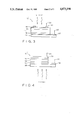
- FIG. 1 is a schematic energy band diagram of a heterojunction p-i-n photovoltaic cell of the present invention
- FIG. 2 is a schematic side elevation view of a first embodiment of a heterojunction p-i-n photovoltaic cell according to the present invention
- FIG. 3 is a schematic side elevation view of a second embodiment thereof.
- FIG. 4 is a schematic side elevation view of a third embodiment thereof.
- Layers are sectioned in FIGS. 2-4 to indicate non-transparency to the incident light.
- FIG. 1 therein illustrated is a schematic energy band diagram for a heterojunction p-i-n photovoltaic cell, such as those illustrated in FIGS. 2-4 and generally designated by the reference numerals 10, 10', and 10", respectively.
- the energy band diagram is a plot of the electron energy against the depth of the cell, in conventional fashion.
- FIG. 2 wherein there is illustrated the first embodiment of a heterojunction p-i-n photovoltaic cell according to the present invention, generally designated by the reference numeral 10.
- the photovoltaic cell 10 which may find utility as a solar cell, is comprised of at least three different semiconductor layers and two ohmic contacts.
- the semiconductor layers are together composed of at least four different elements (exclusive of dopants) and include a p-type relatively wide band gap semiconductor layer 12, a high resistivity intrinsic semiconductor layer 14 used as an absorber of light radiation, and an n-type relatively wide band gap semiconductor layer 16.
- the p-type and n-type layers 12 and 16 are relatively wide band gap "window" layers relative to the narrow band gap "absorber" intrinsic layer.
- the intrinsic layer has an upper surface in electrically conductive contact with the p-type layer 12 and a bottom surface in electrically conductive contact with the n-type layer 16.
- the ohmic contacts 20 and 22 are in electrically conductive contact with the p-type and n-type layers 12 and 16, respectively.
- the term "ohmic contact”, as used herein, refers to materials and structures which produce a low resistance junction with the relevant semiconductor material and allow current to pass freely into an external electrical circuit. It is anticipated that one or more intermediate layers may be required in order to more fully realize the benefits of this device. For example, intermediate layers might be inserted between either electrical contact 20 or 22 and semiconductor layers 12 or 16 in order to improve the quality of the contact, such as by passivating the semiconductor surface 12, 16, by reducing the contact resistance, or by increasing the physical or chemical stability of the interface.
- the three semiconductor layers 12, 14, and 16 are preferably each polycrystalline in nature, such polycrystalline materials frequently being cheaper and more easily deposited than single crystalline materials and affording greater carrier mobility and lifetime than amorphous materials.
- polycrystalline materials are preferred.
- the semiconductor layers 12, 14, and 16 are formed of the II-VI compounds well known for their utility in photovoltaic applications. While binary compounds are preferred, ternary compounds may also be used. More specifically, in the preferred embodiment ZnTe is employed as the p-type layer 12, CdTe as the intrinsic layer 14, and CdS as the n-type layer 16. Advantages of this specific configuration include the fact that CdS prefers to be n-type, ZnTe prefers to be p-type, and CdTe is self-compensating and thus prefers to be intrinsic. The intrinsic layer of CdTe may be electrodeposited on either the p-type layer or the n-type layer. The four different elements in these three semiconductor layers are Zn, Te, Cd, and S.
- this embodiment has the advantage that n-type carriers (electrons) are reflected from the p-type layer by the discontinuity in the conduction band edge at the interface between the intrinsic and p-type layers, and that p-type carriers (holes) are reflected from the n-type layer by the discontinuity in the valence band edge at the junction between the intrinsic and n-type layers.
- This reflection has the effect of reducing the number of holes and electrons reaching the n-type and p-type regions, respectively, thus reducing the number of charge carriers lost via recombination in the n-type and p-type layers.
- binary compound semiconductors often utilize compounds with at least one element in common on each side of the junction. Such binary compounds with a common cation would be expected to have a minimal discontinuity in the conduction band, while such binary compounds with a common anion would be expected to have a minimal discontinuity in the valence band.
- the p-i-n device 10 utilizes a common anion in the valence band edge between the intrinsic and p-type layers and a common cation in the conduction band edge between the intrinsic and n-type layers.
- the p-type layer and n-type layers share neither a common anion nor a common cation.
- the interfaces between adjacent layers are depicted as abrupt in FIGS. 1 and 2, it is expected that real junctions may have a measurable width. Thus it is possible that some interdiffusion will occur at some time during device fabrication or use. This is to be expected especially in the case of junctions consisting of II-VI compound semiconductors which often form solid solutions.
- the compounds ZnTe and CdTe may be viewed as the end points of the solid solution Cd 1-x Zn x Te at which x attains its limiting values of 1 and 0, respectively.
- the solid solution CdS 1-x Te x is known to exist in a continuum of stable compositions. The situation is similar for other compounds. Thus, many variations are possible, and the existence of graded interfaces is to be expected. The merits of such intentionally interdiffused interfaces are not known; however, it is possible that the degree of interdiffusion will affect, and possibly improve, the electrical, optical and chemical properties of the device.
- interface states may have no effect on the operation of a solar cell; in other instances they may even be beneficial.
- interface states are detrimental to the efficient operation of a solar cell. For example, interface states may become charged and thereby decrease the magnitude of the voltage drop, and therefore the penetration of the space charge region, within the absorber semiconductor. This has the effect of reducing both the current and the voltage generated by the solar cell.
- the interface states may serve as recombination centers for minority charge carriers with majority charge carriers, thus reducing the number of photogenerated carriers collected and therefore the current generated by the solar cell.
- This passivation may be accomplished by growing or depositing an intermediate layer at the interface between the two semiconductor materials.
- This intermediate layer might, for example, be composed of an oxide grown onto one of the semiconductors, i.e., a native oxide.
- the intermediate layer might be a compound with no elements in common with either semiconductor material.
- the application of such passivation layers is well known in the photovoltaic art.
- intermediate layers may be inserted between the intrinsic layer 14 and either or both of layers 12 and 16 for the purpose of passivating the interfaces therebetween, or of improving the electrical or optical coupling between layers, or of increasing the chemical or physical stability of the interface.
- an anti-reflection coating 18 may be applied to the upper surface of the p-type layer 12 in order to increase the amount of light entering the device.
- a current collecting grid 24 on top of the p-type layer 12 is employed as part of the ohmic contact 20 and a conducting layer 26 below the n-type layer 16 is part of the ohmic contact 22.
- the conducting layer 26 is non-transparent although a transparent layer could be employed if desired.
- the device (and in particular conducting layer 26) is supported on a substrate 28 which, if desired, may serve as both physical support and as part of the ohmic contact 22.
- FIG. 3 therein illustrated is a second embodiment of the present invention, generally designated by the reference numeral 10', wherein the light is incident through the n-type layer 16.
- the three semiconductor layers are in reverse order from the first embodiment 10, with the n-type layer 16 on top, the intrinsic layer 14 therebelow, and the p-type layer 12 at the bottom.
- the current collecting grid 24 is a component of the ohmic contact 22 in conductive contact with the n-type layer 16 and the non-transparent conducting layer 26 is part of the ohmic contact 20 in conductive contact with the p-type layer 12.
- the anti-reflection layer 18 is, of course, on top of the exposed upper surface of the n-type layer 16 rather than the p-type layer 12.
- FIG. 4 therein illustrated is a third embodiment of the present invention, generally designated by the reference numeral 10".
- the third embodiment 10" is similar to the first embodiment 10 except that the conductive grid 24 is replaced by a continuous conducting layer 30 as part of the ohmic contact 20 to the p-type layer 12, and the ohmic conducting layer 26 is replaced by a transparent conducting layer 32 as part of the ohmic contact 22 to the n-type layer 16.
- the substrate 28 which in the first and second embodiments could, but need not be transparent, is necessarily transparent as the light is incident on the n-type layer 16 through the substrate 28 and conducting layer 32. If desired, an anti-reflection layer may be deposited on the exposed bottom face of the substrate layer 28.
- the ohmic contact 30 to the p-type layer is formed of a material transparent to light of wavelength greater than that absorbed by the intrinsic layer 14. This allows a significant fraction of the radiant energy to pass through the device. This transmitted energy is then available for other applications.
- the p-i-n device may then operate as the top cell in a cascade solar cell. Another lower band gap solar cell placed behind the top cell would then produce additional electrical energy, thus increasing the overall efficiency of the sunlight-to-electricity conversion.
- an ultrasonically cleaned low-sodium, borosilicate glass slide is coated with a transparent oxide front coating such as indium-tin-oxide or tin oxide.
- the CdS film is deposited on the coated glass substrate, for example, by vacuum deposition or by a narrow reaction gap process (as described in co-pending U.S. patent application Ser. No. 863,929, filed May 15, 1986).
- the vacuum deposited layer may be about 1 ⁇ m while the narrow reaction gap process deposited layer is about 1500 ⁇ .
- CdTe is electrodeposited from an aqueous bath containing cadmium and tellurium ions using techniques fully described in U.S. Pat. No. 4,260,427.
- the composite structure is then heat treated, and the CdTe is given a bromine-methanol etching rinse to prepare it for ZnTe deposition.
- a further preparation of the surface may be effected by soaking it in a sodium sulfate/potassium hydroxide solution and rinsing it in deionized water.
- ZnTe is evaporated in a vacuum onto the rinsed surface to the desired thickness (for example, 0.06 ⁇ m to 0.15 ⁇ m).
- vacuum evaporated gold, indium-tin-oxide, or a combination of either with silver-impregnated epoxy may be used as the ohmic back contact to the p-type layer of ZnTe.
- the ohmic contact 20 in conductive contact with the p-type layer 12 may be gold, a silver-containing epoxy, an indium-tin-oxide component or like materials, depending on the intended application.
- the ohmic contact 22 in conductive contact with the n-type layer 16 may be tin oxide, indium-tin-oxide, a silver-containing epoxy or like materials.
- A. CdS on SnO 2 coated glass substrate--CdS is deposited onto a SnO 2 coated glass substrate in a narrow reaction gap process as described in co-pending U.S. patent application Ser. No. 863,929, filed May 15, 1986.
- a mist comprised of 0.05M CdCl 2 and 0.055M thiourea in a nitrogen carrier gas is passed over a substrate heated to approximately 450° C. producing a uniform film of CdS approximately 1500 ⁇ thick.
- CdTe deposition and heat treatment The CdTe layer is electrodeposited from an aqueous bath containing cadmium and tellurium ions using techniques fully described in U.S. Pat. No. 4,260,427.
- the composite structure is next dipped into a 1% solution of CdCl 2 in methanol and dried prior to being heated to 415° C., in air, for twenty minutes.
- ZnTe deposition--ZnTe is thermally evaporated onto bromine-methanol etched CdTe in vacuum.
- the temperature of the CdTe/CdS/SnO 2 /glass is kept at about 260° C. throughout the ZnTe deposition.
- Copper is co-evaporated as a dopant.
- the final ZnTe thickness is 600 ⁇ .
- Vacuum evaporated gold is used as the ohmic back contact to the ZnTe p-type layer.
- a cell was prepared as in Example I except that silver-impregnated epoxy was applied both to the gold contact in order to reduce the sheet resistance of the back contact and to the SnO 2 surrounding the cell in order to reduce the series resistance of the front contact.
- a cell was prepared as in Example II with the following exceptions:
- the ZnTe was deposited at 300° C. to a thickness of 1000 ⁇ .
- the silver impregnated epoxy was applied only at the perimeter of the ITO contact. Although this reduces its effectiveness at reducing the series resistance, this allows light of wavelength greater than that corresponding to the CdTe bandgap (865 nm) to pass through the entire device.
- the optical transmission at 900 nm was 32%, an important property where the cell is to be used as part of a cell cascade.
- a cell was prepared as in Example II with the following exceptions:
- the ZnTe was deposited at 300° C. to a thickness of 1000 ⁇ .
- CdS on ITO coated glass substrate--In vacuum CdS is thermally evaporated from a baffled tungsten boat onto an ultrasonically cleaned, low sodium, borosilicate glass slide coated with 0.2 ⁇ m indium-tin-oxide.
- the temperature of the substrate is maintained between 180°-220° C. during the deposition.
- the deposition rate is about 0.5 ⁇ m per minute, the thickness is in the 1 ⁇ m range.
- the deposited CdS is then heat treated at 400° C. for 30 minutes in a flowing hydrogen atmosphere in order to reduce the excess sulfur content.
- CdTe deposition and heat treatment --The CdTe layer is electrodeposited from an aqueous bath containing cadmium and tellurium ions using techniques fully described in U.S. Pat. No. 4,260,427. The composite structure is then heat treated for one hour in air at 300° C.
- ZnTe deposition--0.15 um ZnTe is thermally evaporated onto bromine-methanol etched CdTe in vacuum.
- the temperature of the CdTe/CdS/ITO/glass is kept at about 250° C. throughout the ZnTe deposition.
- Copper is co-evaporated as a dopant.
- Vacuum evaporated gold is used as the ohmic back contact to the ZnTe p-type layer.
- the present invention combines a minimization of cost of manufacture with a maximization of efficiency.
- Minimization of cost is achieved by the use of thin films (less than 10 microns thick) of selected component materials and by an efficient manufacturing process. More particularly, the use of II-VI compounds as component materials provides not only relatively low material cost, but also ease of deposition of the semiconductor layers.
- Maximization of efficiency is achieved by the proper selection of materials and the design of the photovoltaic cell. The materials are selected to minimize energy band discontinuities or spikes at the interfaces between semiconductors, and the cell design utilizes concepts which are known to produce efficient cells--namely, the p-i-n structure and the heterojunction interface.
- a high optical transmission level enables use of the cell in a cascade; in other particular embodiments an efficiency in excess of 10% is achieved.
Abstract
Description
______________________________________
area                   2.0 mm.sup.2
short circuit current density
                       21.6 mA/cm.sup.2
Open circuit voltaqe   774 mV
fill factor            .64
efficiency             10.7%
______________________________________
______________________________________
area                   4.1 cm.sup.2
short circuit current density
                       21.8 mA/cm.sup.2
open circuit voltage   686 mV
fill factor            .63
efficiency             9.4%
______________________________________
______________________________________
area                   1.44 cm.sup.2
short circuit current density
                       22.9 mA/cm.sup.2
open circuit voltage   688 mV
fill factor            .44
efficiency             6.9%
______________________________________
______________________________________
area                   2.0 mm.sup.2
short circuit current density
                       21.6 mA/cm.sup.2
open circuit voltage   737 mV
fill factor            .63
efficiency             10.0%
______________________________________
______________________________________ area 2 mm.sup.2 short circuitcurrent density 18 mA/cm.sup.2 open circuit voltage 615 mV fill factor .47 efficiency 5.2% ______________________________________
Claims (37)
Priority Applications (2)
| Application Number | Priority Date | Filing Date | Title |
|---|---|---|---|
| US07/203,610 US4873198A (en) | 1986-10-21 | 1988-06-02 | Method of making photovoltaic cell with chloride dip |
| US07/390,986 US4977097A (en) | 1986-10-21 | 1989-08-01 | Method of making heterojunction P-I-N photovoltaic cell |
Applications Claiming Priority (3)
| Application Number | Priority Date | Filing Date | Title |
|---|---|---|---|
| US06/922,122 US4710589A (en) | 1986-10-21 | 1986-10-21 | Heterojunction p-i-n photovoltaic cell |
| US11861087A | 1987-11-09 | 1987-11-09 | |
| US07/203,610 US4873198A (en) | 1986-10-21 | 1988-06-02 | Method of making photovoltaic cell with chloride dip |
Related Parent Applications (1)
| Application Number | Title | Priority Date | Filing Date |
|---|---|---|---|
| US11861087A Division | 1986-10-21 | 1987-11-09 |
Related Child Applications (1)
| Application Number | Title | Priority Date | Filing Date |
|---|---|---|---|
| US07/390,986 Continuation US4977097A (en) | 1986-10-21 | 1989-08-01 | Method of making heterojunction P-I-N photovoltaic cell |
Publications (1)
| Publication Number | Publication Date |
|---|---|
| US4873198A true US4873198A (en) | 1989-10-10 |
Family
ID=27382191
Family Applications (1)
| Application Number | Title | Priority Date | Filing Date |
|---|---|---|---|
| US07/203,610 Expired - Lifetime US4873198A (en) | 1986-10-21 | 1988-06-02 | Method of making photovoltaic cell with chloride dip |
Country Status (1)
| Country | Link |
|---|---|
| US (1) | US4873198A (en) |
Cited By (11)
| Publication number | Priority date | Publication date | Assignee | Title |
|---|---|---|---|---|
| US20050151131A1 (en) * | 2002-06-11 | 2005-07-14 | Wager John F.Iii | Polycrystalline thin-film solar cells |
| US20070184573A1 (en) * | 2006-02-08 | 2007-08-09 | Guardian Industries Corp., | Method of making a thermally treated coated article with transparent conductive oxide (TCO) coating for use in a semiconductor device |
| US20070275252A1 (en) * | 2006-05-23 | 2007-11-29 | Guardian Industries Corp. | Method of making thermally tempered coated article with transparent conductive oxide (TCO) coating in color compression configuration, and product made using same |
| US20100184249A1 (en) * | 2009-01-21 | 2010-07-22 | Yung-Tin Chen | Continuous deposition process and apparatus for manufacturing cadmium telluride photovoltaic devices |
| US20110290308A1 (en) * | 2010-05-28 | 2011-12-01 | General Electric Company | Monolithically integrated solar modules and methods of manufacture |
| US20120097227A1 (en) * | 2010-10-22 | 2012-04-26 | Electronics And Telecommunications Research Institute | Solar cells |
| US20130312824A1 (en) * | 2012-05-21 | 2013-11-28 | First Solar, Inc. | Method of providing chloride treatment for a photovoltaic device and a chloride treated photovoltaic device |
| US20140363918A1 (en) * | 2013-06-10 | 2014-12-11 | Tsmc Solar Ltd. | Apparatus and method for producing solar cells using light treatment |
| US9130113B2 (en) | 2012-12-14 | 2015-09-08 | Tsmc Solar Ltd. | Method and apparatus for resistivity and transmittance optimization in TCO solar cell films |
| US9801726B2 (en) | 2008-02-29 | 2017-10-31 | Arthrex, Inc. | Canine elbow repair and instrumentation |
| CN113828343A (en) * | 2021-10-29 | 2021-12-24 | 厦门理工学院 | GaN ZnO solid solution powder subjected to surface treatment and surface treatment method thereof |
Citations (26)
| Publication number | Priority date | Publication date | Assignee | Title |
|---|---|---|---|---|
| US30412A (en) * | 1860-10-16 | Salem t | ||
| US2651700A (en) * | 1951-11-24 | 1953-09-08 | Francois F Gans | Manufacturing process of cadmium sulfide, selenide, telluride photoconducting cells |
| US3145120A (en) * | 1962-02-12 | 1964-08-18 | Ibm | Method for controlling flux pressure during a sintering process |
| US3261726A (en) * | 1961-10-09 | 1966-07-19 | Monsanto Co | Production of epitaxial films |
| US3374108A (en) * | 1964-06-18 | 1968-03-19 | Kewanee Oil Co | Formation of barrier layers in cadmium sulfide solar cells |
| US3416956A (en) * | 1966-05-16 | 1968-12-17 | Kewanee Oil Co | Process for forming a barrier in a cadmium sulfide solar cell |
| US3754985A (en) * | 1971-04-05 | 1973-08-28 | Photophysics | Process for making a sintered photoconductive body |
| JPS53138288A (en) * | 1977-05-10 | 1978-12-02 | Agency Of Ind Science & Technol | Thin-film solar battery of sintered electrode type |
| US4178395A (en) * | 1977-11-30 | 1979-12-11 | Photon Power, Inc. | Methods for improving solar cell open circuit voltage |
| USRE30412E (en) | 1979-04-26 | 1980-10-07 | Eastman Kodak Company | CdTe Barrier type photovoltaic cells with enhanced open-circuit voltage, and process of manufacture |
| US4231808A (en) * | 1978-09-05 | 1980-11-04 | Fuji Photo Film Co., Ltd. | Thin film photovoltaic cell and a method of manufacturing the same |
| US4255208A (en) * | 1979-05-25 | 1981-03-10 | Ramot University Authority For Applied Research And Industrial Development Ltd. | Method of producing monocrystalline semiconductor films utilizing an intermediate water dissolvable salt layer |
| US4260427A (en) * | 1979-06-18 | 1981-04-07 | Ametek, Inc. | CdTe Schottky barrier photovoltaic cell |
| US4261802A (en) * | 1980-02-21 | 1981-04-14 | Ametek, Inc. | Method of making a photovoltaic cell |
| US4287383A (en) * | 1979-12-26 | 1981-09-01 | Chevron Research Company | Cadmium sulfide photovoltaic cell of improved efficiency |
| US4376795A (en) * | 1980-09-09 | 1983-03-15 | Nippon Telegraph & Telephone Public Corp. | Method of producing image sensor |
| US4379020A (en) * | 1980-06-16 | 1983-04-05 | Massachusetts Institute Of Technology | Polycrystalline semiconductor processing |
| US4388483A (en) * | 1981-09-08 | 1983-06-14 | Monosolar, Inc. | Thin film heterojunction photovoltaic cells and methods of making the same |
| US4400244A (en) * | 1976-06-08 | 1983-08-23 | Monosolar, Inc. | Photo-voltaic power generating means and methods |
| US4425194A (en) * | 1976-06-08 | 1984-01-10 | Monosolar, Inc. | Photo-voltaic power generating means and methods |
| US4548681A (en) * | 1984-02-03 | 1985-10-22 | The Standard Oil Company (Ohio) | Electrodeposition of thin film heterojunction photovoltaic devices that utilize Cd rich Hg1-x Cdx Te |
| US4596645A (en) * | 1984-10-23 | 1986-06-24 | California Institute Of Technology | Reactively-sputtered zinc semiconductor films of high conductivity for heterojunction devices |
| US4642140A (en) * | 1985-04-30 | 1987-02-10 | The United States Of America As Represented By The United States Department Of Energy | Process for producing chalcogenide semiconductors |
| US4710589A (en) * | 1986-10-21 | 1987-12-01 | Ametek, Inc. | Heterojunction p-i-n photovoltaic cell |
| US4759951A (en) * | 1985-09-25 | 1988-07-26 | Sharp Kabushiki Kaisha | Heat-treating Cd-containing photoelectric conversion film in the presence of a cadmium halide |
| US4816120A (en) * | 1986-05-06 | 1989-03-28 | The Standard Oil Company | Electrodeposited doped II-VI semiconductor films and devices incorporating such films |
-
1988
- 1988-06-02 US US07/203,610 patent/US4873198A/en not_active Expired - Lifetime
Patent Citations (26)
| Publication number | Priority date | Publication date | Assignee | Title |
|---|---|---|---|---|
| US30412A (en) * | 1860-10-16 | Salem t | ||
| US2651700A (en) * | 1951-11-24 | 1953-09-08 | Francois F Gans | Manufacturing process of cadmium sulfide, selenide, telluride photoconducting cells |
| US3261726A (en) * | 1961-10-09 | 1966-07-19 | Monsanto Co | Production of epitaxial films |
| US3145120A (en) * | 1962-02-12 | 1964-08-18 | Ibm | Method for controlling flux pressure during a sintering process |
| US3374108A (en) * | 1964-06-18 | 1968-03-19 | Kewanee Oil Co | Formation of barrier layers in cadmium sulfide solar cells |
| US3416956A (en) * | 1966-05-16 | 1968-12-17 | Kewanee Oil Co | Process for forming a barrier in a cadmium sulfide solar cell |
| US3754985A (en) * | 1971-04-05 | 1973-08-28 | Photophysics | Process for making a sintered photoconductive body |
| US4400244A (en) * | 1976-06-08 | 1983-08-23 | Monosolar, Inc. | Photo-voltaic power generating means and methods |
| US4425194A (en) * | 1976-06-08 | 1984-01-10 | Monosolar, Inc. | Photo-voltaic power generating means and methods |
| JPS53138288A (en) * | 1977-05-10 | 1978-12-02 | Agency Of Ind Science & Technol | Thin-film solar battery of sintered electrode type |
| US4178395A (en) * | 1977-11-30 | 1979-12-11 | Photon Power, Inc. | Methods for improving solar cell open circuit voltage |
| US4231808A (en) * | 1978-09-05 | 1980-11-04 | Fuji Photo Film Co., Ltd. | Thin film photovoltaic cell and a method of manufacturing the same |
| USRE30412E (en) | 1979-04-26 | 1980-10-07 | Eastman Kodak Company | CdTe Barrier type photovoltaic cells with enhanced open-circuit voltage, and process of manufacture |
| US4255208A (en) * | 1979-05-25 | 1981-03-10 | Ramot University Authority For Applied Research And Industrial Development Ltd. | Method of producing monocrystalline semiconductor films utilizing an intermediate water dissolvable salt layer |
| US4260427A (en) * | 1979-06-18 | 1981-04-07 | Ametek, Inc. | CdTe Schottky barrier photovoltaic cell |
| US4287383A (en) * | 1979-12-26 | 1981-09-01 | Chevron Research Company | Cadmium sulfide photovoltaic cell of improved efficiency |
| US4261802A (en) * | 1980-02-21 | 1981-04-14 | Ametek, Inc. | Method of making a photovoltaic cell |
| US4379020A (en) * | 1980-06-16 | 1983-04-05 | Massachusetts Institute Of Technology | Polycrystalline semiconductor processing |
| US4376795A (en) * | 1980-09-09 | 1983-03-15 | Nippon Telegraph & Telephone Public Corp. | Method of producing image sensor |
| US4388483A (en) * | 1981-09-08 | 1983-06-14 | Monosolar, Inc. | Thin film heterojunction photovoltaic cells and methods of making the same |
| US4548681A (en) * | 1984-02-03 | 1985-10-22 | The Standard Oil Company (Ohio) | Electrodeposition of thin film heterojunction photovoltaic devices that utilize Cd rich Hg1-x Cdx Te |
| US4596645A (en) * | 1984-10-23 | 1986-06-24 | California Institute Of Technology | Reactively-sputtered zinc semiconductor films of high conductivity for heterojunction devices |
| US4642140A (en) * | 1985-04-30 | 1987-02-10 | The United States Of America As Represented By The United States Department Of Energy | Process for producing chalcogenide semiconductors |
| US4759951A (en) * | 1985-09-25 | 1988-07-26 | Sharp Kabushiki Kaisha | Heat-treating Cd-containing photoelectric conversion film in the presence of a cadmium halide |
| US4816120A (en) * | 1986-05-06 | 1989-03-28 | The Standard Oil Company | Electrodeposited doped II-VI semiconductor films and devices incorporating such films |
| US4710589A (en) * | 1986-10-21 | 1987-12-01 | Ametek, Inc. | Heterojunction p-i-n photovoltaic cell |
Non-Patent Citations (36)
| Title |
|---|
| Arndt et al., Large Bandgap Polycrystalline Thin Film Solar Cells for Tandem Structures, Tech. Digest Inter l PVSEC 1, pp. 361 364 (1984). * |
| Arndt et al., Large Bandgap Polycrystalline Thin Film Solar Cells for Tandem Structures, Tech. Digest Inter'l PVSEC-1, pp. 361-364 (1984). |
| Japanese Journal of Applied Physics, vol. 15 (1976), No. 11, pp. 2281 2283. * |
| Japanese Journal of Applied Physics, vol. 15 (1976), No. 11, pp. 2281-2283. |
| Japanese Journal of Applied Physics, vol. 17 (1978), No. 3, pp. 585 586. * |
| Japanese Journal of Applied Physics, vol. 17 (1978), No. 3, pp. 585-586. |
| Japanese Journal of Applied Physics, vol. 19 (1980), No. 1, pp. 129 134. * |
| Japanese Journal of Applied Physics, vol. 19 (1980), No. 1, pp. 129-134. |
| Japanese Journal of Applied Physics, vol. 19 (1980), No. 4, pp. 703 712. * |
| Japanese Journal of Applied Physics, vol. 19 (1980), No. 4, pp. 703-712. |
| Japanese Journal of Applied Physics, vol. 21 (1982), No. 5, pp. 800 801. * |
| Japanese Journal of Applied Physics, vol. 21 (1982), No. 5, pp. 800-801. |
| Japanese Journal of Applied Physics, vol. 21, (1982), Supplement 21 2, pp. 103 107. * |
| Japanese Journal of Applied Physics, vol. 21, (1982), Supplement 21-2, pp. 103-107. |
| Japanese Journal of Applied Physics, vol. 22 (1983), No. 2, pp. 269 271. * |
| Japanese Journal of Applied Physics, vol. 22 (1983), No. 2, pp. 269-271. |
| Loferski, Theoretical & Experimental Studies of Tandem or Cascade Solar Cells: A Review, Conf. Rec. 16 th IEEE Photovoltaic Spec. Conf., pp. 648 654 (1982). * |
| Loferski, Theoretical & Experimental Studies of Tandem or Cascade Solar Cells: A Review, Conf. Rec. 16th IEEE Photovoltaic Spec. Conf., pp. 648-654 (1982). |
| Matsushita News MEP 83 2, dated Feb. 1, 1983. * |
| Matsushita News MEP-83-2, dated Feb. 1, 1983. |
| N. Nakayama et al., Japanese J. Appl. d Phys. , vol. 19, pp. 703 712 (1980). * |
| N. Nakayama et al., Japanese J. Appl.'d Phys., vol. 19, pp. 703-712 (1980). |
| P. V. Meyers, "Polycrystalline CdS/CdTe/ZnTe n-i-p Solar Cell", Seventh European Community Photovoltaic Conference, Seville, Spain, Oct. 27-31, 1986. |
| P. V. Meyers, Polycrystalline CdS/CdTe/ZnTe n i p Solar Cell , Seventh European Community Photovoltaic Conference , Seville, Spain, Oct. 27 31, 1986. * |
| R. Radojcic et al., Solar Cells , vol. 4, pp. 121 126 (1981). * |
| R. Radojcic et al., Solar Cells, vol. 4, pp. 121-126 (1981). |
| Razykov et al., Photovoltaic Effect in Heterojunctions Made of Zinc and Cadmium Telluride, Sov. Phys. Semiconductors , vol. 17, pp. 585 586 (1983). * |
| Razykov et al., Photovoltaic Effect in Heterojunctions Made of Zinc and Cadmium Telluride, Sov. Phys. Semiconductors, vol. 17, pp. 585-586 (1983). |
| Spitzer et al., Theoretical Limit Efficiency of Direct Gap Solar Cells, Conf. Rec. 14 th IEEEE Photovoltaic Spec. Conf. , pp. 585 590 (1980). * |
| Spitzer et al., Theoretical Limit Efficiency of Direct Gap Solar Cells, Conf. Rec. 14th IEEEE Photovoltaic Spec. Conf., pp. 585-590 (1980). |
| Spitzer et al., Ultra High Efficiency Thin Silicon P N Junction Solar Cells Using Reflecting Surfaces, Conf. Rec. 14 th IEEE Photovoltaic Spec. Conf. , pp. 375 380 (1980). * |
| Spitzer et al., Ultra High Efficiency Thin Silicon P-N Junction Solar Cells Using Reflecting Surfaces, Conf. Rec. 14th IEEE Photovoltaic Spec. Conf., pp. 375-380 (1980). |
| Weideman et al., Achievement of Higher Efficiency Amorphous Silicon Germanium Solar Cells Using Affinity Gradients, Conf. Rec. 17 th IEEE Photovoltaic Spec. Conf. , pp. 223 228 (1984). * |
| Weideman et al., Achievement of Higher Efficiency Amorphous Silicon-Germanium Solar Cells Using Affinity Gradients, Conf. Rec. 17th IEEE Photovoltaic Spec. Conf., pp. 223-228 (1984). |
| Wolf, Designing Practical Silicon Solar Cells Approaching the "Limit Conversion Efficiency", Conf. Rec. 14th IEEE Photovoltaic Spec. Conf., pp. 563-568 (1980). |
| Wolf, Designing Practical Silicon Solar Cells Approaching the Limit Conversion Efficiency , Conf. Rec. 14 th IEEE Photovoltaic Spec. Conf. , pp. 563 568 (1980). * |
Cited By (18)
| Publication number | Priority date | Publication date | Assignee | Title |
|---|---|---|---|---|
| US20050151131A1 (en) * | 2002-06-11 | 2005-07-14 | Wager John F.Iii | Polycrystalline thin-film solar cells |
| US20070184573A1 (en) * | 2006-02-08 | 2007-08-09 | Guardian Industries Corp., | Method of making a thermally treated coated article with transparent conductive oxide (TCO) coating for use in a semiconductor device |
| US8298380B2 (en) | 2006-05-23 | 2012-10-30 | Guardian Industries Corp. | Method of making thermally tempered coated article with transparent conductive oxide (TCO) coating in color compression configuration, and product made using same |
| US20070275252A1 (en) * | 2006-05-23 | 2007-11-29 | Guardian Industries Corp. | Method of making thermally tempered coated article with transparent conductive oxide (TCO) coating in color compression configuration, and product made using same |
| US9801726B2 (en) | 2008-02-29 | 2017-10-31 | Arthrex, Inc. | Canine elbow repair and instrumentation |
| US7901975B2 (en) * | 2009-01-21 | 2011-03-08 | Yung-Tin Chen | Continuous deposition process and apparatus for manufacturing cadmium telluride photovoltaic devices |
| US20100184249A1 (en) * | 2009-01-21 | 2010-07-22 | Yung-Tin Chen | Continuous deposition process and apparatus for manufacturing cadmium telluride photovoltaic devices |
| CN102299158A (en) * | 2010-05-28 | 2011-12-28 | 通用电气公司 | Monolithically integrated solar modules and methods of manufacture |
| US20110290308A1 (en) * | 2010-05-28 | 2011-12-01 | General Electric Company | Monolithically integrated solar modules and methods of manufacture |
| CN102299158B (en) * | 2010-05-28 | 2016-05-25 | 通用电气公司 | Monolithic integrated solar module and manufacture method |
| US20120097227A1 (en) * | 2010-10-22 | 2012-04-26 | Electronics And Telecommunications Research Institute | Solar cells |
| US20130312824A1 (en) * | 2012-05-21 | 2013-11-28 | First Solar, Inc. | Method of providing chloride treatment for a photovoltaic device and a chloride treated photovoltaic device |
| CN104737303A (en) * | 2012-05-21 | 2015-06-24 | 第一太阳能有限公司 | Method of providing chloride treatment for a photovoltaic device and a chloride treated photovoltaic device |
| US9147792B2 (en) * | 2012-05-21 | 2015-09-29 | First Solar, Inc. | Method of providing chloride treatment for a photovoltaic device and a chloride treated photovoltaic device |
| US9130113B2 (en) | 2012-12-14 | 2015-09-08 | Tsmc Solar Ltd. | Method and apparatus for resistivity and transmittance optimization in TCO solar cell films |
| US20140363918A1 (en) * | 2013-06-10 | 2014-12-11 | Tsmc Solar Ltd. | Apparatus and method for producing solar cells using light treatment |
| CN113828343A (en) * | 2021-10-29 | 2021-12-24 | 厦门理工学院 | GaN ZnO solid solution powder subjected to surface treatment and surface treatment method thereof |
| CN113828343B (en) * | 2021-10-29 | 2023-05-23 | 厦门理工学院 | Surface-treated GaN-ZnO solid solution powder and surface treatment method thereof |
Similar Documents
| Publication | Publication Date | Title |
|---|---|---|
| US4710589A (en) | Heterojunction p-i-n photovoltaic cell | |
| US5137835A (en) | Method for manufacturing a chalcopyrite solar cell | |
| US5125984A (en) | Induced junction chalcopyrite solar cell | |
| US4239553A (en) | Thin film photovoltaic cells having increased durability and operating life and method for making same | |
| US5286306A (en) | Thin film photovoltaic cells from I-III-VI-VII compounds | |
| US4626322A (en) | Photoelectrochemical preparation of a solid-state semiconductor photonic device | |
| CA1275316C (en) | Photovoltaic heterojunction structures | |
| Dharmadasa et al. | New ways of developing glass/conducting glass/CdS/CdTe/metal thin-film solar cells based on a new model | |
| EP2136413A2 (en) | Photovoltaic device | |
| JPH0557746B2 (en) | ||
| US4977097A (en) | Method of making heterojunction P-I-N photovoltaic cell | |
| US4492811A (en) | Heterojunction photovoltaic device | |
| US4873198A (en) | Method of making photovoltaic cell with chloride dip | |
| US20170243999A1 (en) | Solar cell | |
| Wilson et al. | Amorphous-silicon mis solar cells | |
| JPH11150282A (en) | Photovoltaic element and its manufacture | |
| EP0248953A1 (en) | Tandem photovoltaic devices | |
| CN114335348B (en) | PN heterojunction antimony selenide/perovskite solar cell and preparation method thereof | |
| Basol et al. | Thin films of mercury cadmium telluride for solar cell applications | |
| US4608750A (en) | Preparation of photovoltaic device by electrochemical deposition | |
| US4644638A (en) | Photovoltaic device prepared by electroless deposition | |
| JP3130993B2 (en) | Solar cell | |
| Lokhande et al. | Effect of aluminum doping on the properties of PEC cells formed with CdS: Al films | |
| WO2004084282A1 (en) | Bifacial structure for tandem solar cell formed with amorphous semiconductor materials | |
| KR20110116485A (en) | Method for fabricating solar cell |
Legal Events
| Date | Code | Title | Description |
|---|---|---|---|
| AS | Assignment |
Owner name: AMETEK, INC., A NY CORP., PENNSYLVANIA Free format text: ASSIGNMENT OF ASSIGNORS INTEREST.;ASSIGNORS:MEYERS, PETER V.;LIU, CHUNG-HENG;DOTY, MITCHELL E.;REEL/FRAME:005002/0507 Effective date: 19881103 |
|
| STCF | Information on status: patent grant |
Free format text: PATENTED CASE |
|
| CC | Certificate of correction | ||
| AS | Assignment |
Owner name: COLORADO SCHOOL OF MINES FOUNDATION, INC., STE. 34 Free format text: ASSIGNMENT OF ASSIGNORS INTEREST.;ASSIGNOR:AMETEK, INC.;REEL/FRAME:005610/0762 Effective date: 19910225 |
|
| FPAY | Fee payment |
Year of fee payment: 4 |
|
| FPAY | Fee payment |
Year of fee payment: 8 |
|
| AS | Assignment |
Owner name: COLORADO SCHOOL OF MINES FOUNDATION INCORPORATED, Free format text: LICENSE AGREEMENT;ASSIGNOR:SOLAR CELLS, INC.;REEL/FRAME:008621/0724 Effective date: 19970714 |
|
| FPAY | Fee payment |
Year of fee payment: 12 |
|
| AS | Assignment |
Owner name: FIRST SOLAR, INC., OHIO Free format text: ASSIGNMENT OF ASSIGNORS INTEREST;ASSIGNOR:COLORADO SCHOOL OF MINES FOUNDATION INCORPORATED;REEL/FRAME:015215/0510 Effective date: 20030423 |
|
| AS | Assignment |
Owner name: FIRST SOLAR U.S. MANUFACTURING, LLC, OHIO Free format text: ASSIGNMENT OF ASSIGNORS INTEREST;ASSIGNOR:FIRST SOLAR, INC.;REEL/FRAME:018224/0607 Effective date: 20060829 |
|
| AS | Assignment |
Owner name: FIRST SOLAR, INC., OHIO Free format text: MERGER;ASSIGNOR:FIRST SOLAR US MANUFACTURING, LLC;REEL/FRAME:019605/0311 Effective date: 20070331 Owner name: FIRST SOLAR, INC.,OHIO Free format text: MERGER;ASSIGNOR:FIRST SOLAR US MANUFACTURING, LLC;REEL/FRAME:019605/0311 Effective date: 20070331 |