US4870382A - High frequency lock detecting circuit - Google Patents
High frequency lock detecting circuit Download PDFInfo
- Publication number
- US4870382A US4870382A US07/222,699 US22269988A US4870382A US 4870382 A US4870382 A US 4870382A US 22269988 A US22269988 A US 22269988A US 4870382 A US4870382 A US 4870382A
- Authority
- US
- United States
- Prior art keywords
- signal
- coupled
- lock
- high frequency
- phase
- Prior art date
- Legal status (The legal status is an assumption and is not a legal conclusion. Google has not performed a legal analysis and makes no representation as to the accuracy of the status listed.)
- Expired - Lifetime
Links
Images


Classifications
-
- H—ELECTRICITY
- H03—ELECTRONIC CIRCUITRY
- H03L—AUTOMATIC CONTROL, STARTING, SYNCHRONISATION, OR STABILISATION OF GENERATORS OF ELECTRONIC OSCILLATIONS OR PULSES
- H03L7/00—Automatic control of frequency or phase; Synchronisation
- H03L7/06—Automatic control of frequency or phase; Synchronisation using a reference signal applied to a frequency- or phase-locked loop
- H03L7/08—Details of the phase-locked loop
- H03L7/085—Details of the phase-locked loop concerning mainly the frequency- or phase-detection arrangement including the filtering or amplification of its output signal
- H03L7/095—Details of the phase-locked loop concerning mainly the frequency- or phase-detection arrangement including the filtering or amplification of its output signal using a lock detector
-
- Y—GENERAL TAGGING OF NEW TECHNOLOGICAL DEVELOPMENTS; GENERAL TAGGING OF CROSS-SECTIONAL TECHNOLOGIES SPANNING OVER SEVERAL SECTIONS OF THE IPC; TECHNICAL SUBJECTS COVERED BY FORMER USPC CROSS-REFERENCE ART COLLECTIONS [XRACs] AND DIGESTS
- Y10—TECHNICAL SUBJECTS COVERED BY FORMER USPC
- Y10S—TECHNICAL SUBJECTS COVERED BY FORMER USPC CROSS-REFERENCE ART COLLECTIONS [XRACs] AND DIGESTS
- Y10S331/00—Oscillators
- Y10S331/02—Phase locked loop having lock indicating or detecting means
Definitions
- the present invention is related to lock detectors for high speed phase locked loops of the type employed in quadrature phase shift key (QPSK) receivers. More particularly, the present invention relates to a high speed and high frequency function generators and analog multipliers which eliminate the need for low frequency analog multipliers and frequency squaring multipliers which limit the useful frequency of a lock detector.
- QPSK quadrature phase shift key
- the prior art QPSK lock detectors will be described in more detail in the description of the prior art drawings.
- the prior art includes Costas type signal carrier tracking loops which include hard limiters, analog multipliers and square law multipliers.
- the problem with such prior art lock detectors is that they employ components which limit the operation frequency of the lock detector to about 25 megahertz when implemented with semi-conductor devices that high higher operational frequencies.
- a QPSK receiver employs two data tracking loops, one for in-phase and one for quadrature phase data tracking.
- the two data tracking loops are cross coupled so that the lock detectors must pass or process much higher frequency signals than the data rate signals, thus, limiting the data rate to approximately one-half the operational frequency of the components employed in the elements of the prior art lock detectors.
- a high frequency lock detector circuit for generating a signal indicative of a locked or a not locked phase tracking condition and a phase locked loop.
- the lock detector comprises high speed function generators coupled to the modulated data streams for indicating the phase of the data streams and a high speed function generator coupled to the voltage error signal of the phase locked loop to indicate the absence or presence of a voltage error signal.
- the analog outputs of the function generators are summed together in a summing circuit and applied to a differential amplifier which removes the cross modulated data products from the output of the function generators and provides a signal which is supplied to the sweep controls of the phase locked loop when a not locked condition is sensed.
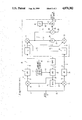
- FIG. 1 is a block diagram of a modified prior art Costas type phase locked loop for a QPSK receiver
- FIG. 2 is a block diagram of the preferred embodiment of the present invention lock detector which may be connected in the phase locked loop of FIG. 1;
- FIG. 3 is a detailed block diagram of one of the function generators which operate as an analog absolute value detector.
- FIG. 1 showing a block diagram of a modified Costas type phase locked loop 10 which comprises a quadrature hybrid phase detector 11 and a lock detector 12.
- a QPSK signal is applied to input line 13 to the quadrature hybrid phase detector 11.
- the signal on line 13 is applied as an input to mixer 14 which also has an input signal from the voltage controlled oscillator.
- the output of mixer 14 on line 16 as applied to a low pass filter 17 to produce an output signal on line 18.
- the signal on line 18 is a data modulated signal which is identified as signal Y for purposes of explaining the present invention.
- the data modulated signal on line 18 is applied to a hard limiter 19 to produce a hard limited output signal on line 21 which is applied to an analog multiplier 22.
- the output of analog multiplier 22 on line 23 is applied to the positive input of a summing circuit 24 to produce an error voltage signal on line 25 which is applied to the loop filter 26.
- the output of the loop filter 26 on line 27 is applied to the voltage controlled oscillator 28 to control the voltage controlled oscillator 28 and track the incoming carrier signal on line 13.
- the output of the voltage controlled oscillator on line 29 is applied to mixer 14 to produce the aforementioned signal on line 16 and is also applied to a 90° phase shifter 31 whose shifted output signal on line 32 is applied to mixer 15 to produce the quadrature data modulated signal on line 33.
- the signal on line 33 is a applied to a low pass filter 34 to produce a filtered data modulated signal (X signal) on line 35 which is applied to a second hard limiter 36 to produce the hard limited data modulated signal on line 37.
- the signal on line 37 is applied to a second analog multiplier 38 which has a cross-channel data modulated signal from line 18 also applied to produce a cross-channel data modulated product signal on line 39 similar to the cross-channel data product modulated signal on line 23 from analog multiplier 22.
- the signal on line 39 is applied to the negative input of the summing circuit 24 to produce the aforementioned voltage error signal on line 25 which is employed to control the frequency of the voltage controlled oscillator 28 and produce the lock on or tracking frequency on line 29.
- the lock detector 12 is shown including the portion of the QPSK receiver which generates the error voltage signal on line 25 which is employed in the lock detector portion of the QPSK receiver.
- the output of summing circuit 24 on line 25 is applied to square law multiplier 41 which produces a signal on line 42 that is basically a rectified version of the beat frequency signal on line 25.
- the signal on line 42 is applied to the negative input of summing circuit 42.
- a third analog multiplier 44 is shown having input lines 23 and 39 applied-thereto to produce an output signal on line 45 which is applied to the positive input of summing circuit 43 to produce the locked or not locked condition or signal on line 46.
- the locked or not locked condition on line 46 is shown being applied to the sweep control 47 to produce a control signal on line 48 to the voltage controlled oscillator 28 which causes the voltage controlled oscillator to sweep through a predetermined frequency range in an attempt to recover the carrier.
- the voltage controlled oscillator is locked on the frequency of the incoming QPSK signal in the preferred embodiment, the voltage error signal on line 25 is a low DC signal and when the VCO 28 is not locked on the incoming carrier signal a beat note signal appears on line 25.
- the signal on line 46 being applied to the sweep control circuit 47 is a high DC signal and when the not locked condition occurs the signal on line 46 is substantially zero.
- the prior art analog multipliers 22, 38 and 44 are basically limited to frequencies of approximately 50 megahertz at their outputs.
- the square law multiplier 41 is basically a low frequency analog multiplier which does not require high frequency response but is an expensive component. As will be discussed in detail hereinafter these expensive components and the analog multipliers which limit the frequency response of the phase locked loop and lock detector can be eliminated in the preferred embodiment of the present invention to be explained hereinafter.
- FIG. 2 showing a preferred embodiment lock detector 49 which comprises a preferred embodiment phase detector of the type shown and described in our co-pending application Ser. No. 222,700.
- the portion of the receiver 10 shown in FIG. 1 producing Y and X signals on lines 18 and 35 has been omitted from the FIG. 2 embodiment.
- the inputs Y and X on lines 18 and 35 are shown being applied to comparators 51, 51' and electronic switches 52, 52' which comprise the function generators to be described in detail hereinafter.
- the comparator 51 is shown producing a Qy output on line 53 and a Qy on line 54 which are applied to the electronic switches 52, 52', 55 and 55'.
- the output from the electronic switches 52 and 52' are shown as positive and negative functions of the inputs X and Y on lines 56 to 59.
- the outputs from the electronic switches 55 and 55' are shown as composite or product function of the input of the X and Y signals multiplied by the function of the Y and X functions respectively on lines 61 and 62.
- the output from the differential amplifier 63 on line 64 is the aforementioned error voltage signal which is applied to the voltage controlled oscillator 28 to control its frequency.
- This same error voltage signal on line 64 is applied as an error voltage signal to the comparator 64 and the electronic switch 66 to produce signals on lines 67 and 68 from the positive and negative outputs of the electronic switch 66 which are deisgnated as -f(E s ) and +f(E s ) respectively.
- the signals on lines 56 to 59 and 67 to 68 are applied to the positive and negative summing nodes 71 and 72 which are in turn connected to the positive and negative inputs of differential amplifier 73 which produces the locked or not locked signal on line 74.
- the output signal is the aboslute value of X plus the absolute value Y minus the absolute value of E S the error signal.
- comparators 51, 51' and electronic switches 52, 52', 55' comprise function generators. Further, comparators 51, 51' and electronic switch 55 also comprise function generators.
- a fifth function generator comprises comparator 65 and electronic switch 66.
- FIG. 3 is a block diagram of a typical function generator of the type employed in the preferred embodiment of FIG. 2.
- the function generator being explained in FIG. 2 is the function generator comprised of comparator 65, electronic switch 66 and differential amplifier 73.
- One of the signals being applied to the positive and negative summing nodes 71 and 72 will be explained as appearing on the output line 74, however, it will be understood that similar function generators applying their outputs on lines 56 to 59 to the same positive and negative summing nodes 71 and 72 will also produce similar outputs as the function generator shown and described herein.
- the voltage error signal E s on line 64 is shown as the data inut to the electronic switch 66.
- the voltage error signal E S on line 64 is shown being applied to the comparator 65 as the control signal which provides two outputs, Q E and Q E also applied to the electronic switch 66.
- the control signal on line 64 When the control signal on line 64 is low, it produces a high output signal Q E which is applied to the gates of the field effect transistors T1 and T4 causing them to conduct.
- the input signal on line 64 is gated to the positive output of the electronic switch 66 and to the positive summing node 71.
- the control signal E S on line 64 is high, the output Q E is high and the gates of transistors T2 and T3 are high causing them to conduct.
- the input signal E S on line 64 is passed to the negative summing node 72 which is connected to the negative side of differential amplifier 73 which produces the error signal on line 74 shown as minus the absolute value of E S .
- the additional input lines to the summing nodes 71 and 72 shown as lines 56 to 59 when fully connected also apply their signals to the summing nodes 71 and 72 to produce the absolute value output shown in FIG. 2.
- the signals being applied to lines 56 to 59 are not shown as output on line 74.
- the error signal E s on line 74 in FIG. 2 is the signal that is applied on line 46 to the sweep control circuit 47 in FIG. 1 to cause the sweep control to sweep the voltage controlled oscillator 28 through a predetermined frequency range in order to achieve tracking or lock on.
- the signal on line 74 in FIG. 3, shown as the negative absolute value of E S is not the complete signal which is applied on line 46 to cause the sweep control circuit 47 to be actuated but includes the absolute value of X and Y as shown in FIG. 2.
- the electronic switches and comparators like 52, 55 may be implemented in gallium arsenide to achieve switching rates as high as 5 gigahertz and when the function generator of FIG. 3 is substituted into the preferred embodiment circuitry of FIG. 2, the preferred embodiment lock detector of FIG. 2 may be incorporated into the block 12 of FIG. 1 to provide a QPSK receiver capable of tracking input data rate signals as high as 5 gigahertz.
- the components required to implement the function generator of FIG. 3 are commercially available.
- the operational amplifier 73 need not be implemented in gallium arsenide because the high frequency modulated cross products are eliminated in the differential amplifier.
- the switching rate or operational switching rate of the differential amplifier 73 preferably need only go to approximately 1 megahertz in order to accommodate incoming data rates of 5 gigahertz.
Abstract
Description
Claims (8)
Priority Applications (1)
| Application Number | Priority Date | Filing Date | Title |
|---|---|---|---|
| US07/222,699 US4870382A (en) | 1988-07-22 | 1988-07-22 | High frequency lock detecting circuit |
Applications Claiming Priority (1)
| Application Number | Priority Date | Filing Date | Title |
|---|---|---|---|
| US07/222,699 US4870382A (en) | 1988-07-22 | 1988-07-22 | High frequency lock detecting circuit |
Publications (1)
| Publication Number | Publication Date |
|---|---|
| US4870382A true US4870382A (en) | 1989-09-26 |
Family
ID=22833319
Family Applications (1)
| Application Number | Title | Priority Date | Filing Date |
|---|---|---|---|
| US07/222,699 Expired - Lifetime US4870382A (en) | 1988-07-22 | 1988-07-22 | High frequency lock detecting circuit |
Country Status (1)
| Country | Link |
|---|---|
| US (1) | US4870382A (en) |
Cited By (11)
| Publication number | Priority date | Publication date | Assignee | Title |
|---|---|---|---|---|
| US5063577A (en) * | 1989-12-12 | 1991-11-05 | Unisys Corporation | High-speed bit synchronizer |
| US5121071A (en) * | 1991-07-31 | 1992-06-09 | Loral Aerospace Corp. | Lock detector for unbalanced QPSK demodulators |
| US5568521A (en) * | 1993-09-16 | 1996-10-22 | Unisys Corporation | Phase lock indicator circuit for a high frequency recovery loop |
| US5592513A (en) * | 1994-04-05 | 1997-01-07 | Scientific-Atlanta, Inc. | Synchronous modulator and methods for synchronous modulation |
| US5703526A (en) * | 1995-07-06 | 1997-12-30 | Sgs-Thomson Microelectronics S.A. | Circuit for detecting the locked condition of PSK or QAM demodulators |
| US5870002A (en) * | 1997-06-23 | 1999-02-09 | Exar Corporation | Phase-frequency lock detector |
| US5924115A (en) * | 1996-03-29 | 1999-07-13 | Interval Research Corporation | Hierarchical memory architecture for a programmable integrated circuit having an interconnect structure connected in a tree configuration |
| US6707863B1 (en) * | 1999-05-04 | 2004-03-16 | Northrop Grumman Corporation | Baseband signal carrier recovery of a suppressed carrier modulation signal |
| US6785354B1 (en) * | 2000-11-28 | 2004-08-31 | Intel Corporation | Lock detection system for use in high speed communication systems |
| US20060038595A1 (en) * | 2004-08-11 | 2006-02-23 | Micron Technology, Inc. | Digital lock detector for PLL |
| US9252788B1 (en) | 2014-09-11 | 2016-02-02 | International Business Machines Corporation | Phase error detection in phase lock loop and delay lock loop devices |
Citations (1)
| Publication number | Priority date | Publication date | Assignee | Title |
|---|---|---|---|---|
| US4092606A (en) * | 1977-06-21 | 1978-05-30 | Lovelace Alan M Acting Adminis | Quadraphase demodulation |
-
1988
- 1988-07-22 US US07/222,699 patent/US4870382A/en not_active Expired - Lifetime
Patent Citations (1)
| Publication number | Priority date | Publication date | Assignee | Title |
|---|---|---|---|---|
| US4092606A (en) * | 1977-06-21 | 1978-05-30 | Lovelace Alan M Acting Adminis | Quadraphase demodulation |
Cited By (17)
| Publication number | Priority date | Publication date | Assignee | Title |
|---|---|---|---|---|
| US5063577A (en) * | 1989-12-12 | 1991-11-05 | Unisys Corporation | High-speed bit synchronizer |
| US5121071A (en) * | 1991-07-31 | 1992-06-09 | Loral Aerospace Corp. | Lock detector for unbalanced QPSK demodulators |
| US5568521A (en) * | 1993-09-16 | 1996-10-22 | Unisys Corporation | Phase lock indicator circuit for a high frequency recovery loop |
| US5592513A (en) * | 1994-04-05 | 1997-01-07 | Scientific-Atlanta, Inc. | Synchronous modulator and methods for synchronous modulation |
| US5596606A (en) * | 1994-04-05 | 1997-01-21 | Scientific-Atlanta, Inc. | Synchronous detector and methods for synchronous detection |
| US5703526A (en) * | 1995-07-06 | 1997-12-30 | Sgs-Thomson Microelectronics S.A. | Circuit for detecting the locked condition of PSK or QAM demodulators |
| US5861773A (en) * | 1995-07-06 | 1999-01-19 | Sgs-Thomson Microelectronics S.A. | Circuit for detecting the locked condition of PSK or QAM |
| US5924115A (en) * | 1996-03-29 | 1999-07-13 | Interval Research Corporation | Hierarchical memory architecture for a programmable integrated circuit having an interconnect structure connected in a tree configuration |
| US5870002A (en) * | 1997-06-23 | 1999-02-09 | Exar Corporation | Phase-frequency lock detector |
| US6707863B1 (en) * | 1999-05-04 | 2004-03-16 | Northrop Grumman Corporation | Baseband signal carrier recovery of a suppressed carrier modulation signal |
| US6785354B1 (en) * | 2000-11-28 | 2004-08-31 | Intel Corporation | Lock detection system for use in high speed communication systems |
| US20060038595A1 (en) * | 2004-08-11 | 2006-02-23 | Micron Technology, Inc. | Digital lock detector for PLL |
| US7424082B2 (en) | 2004-08-11 | 2008-09-09 | Micron Technology, Inc. | Digital lock detector for PLL |
| US9252788B1 (en) | 2014-09-11 | 2016-02-02 | International Business Machines Corporation | Phase error detection in phase lock loop and delay lock loop devices |
| US9590643B2 (en) | 2014-09-11 | 2017-03-07 | International Business Machines Corporation | Phase error detection in phase lock loop and delay lock loop devices |
| US9735789B2 (en) | 2014-09-11 | 2017-08-15 | International Business Machines Corporation | Phase error detection in phase lock loop and delay lock loop devices |
| US10164648B2 (en) | 2014-09-11 | 2018-12-25 | International Business Machines Corporation | Phase error detection in phase lock loop and delay lock loop devices |
Similar Documents
| Publication | Publication Date | Title |
|---|---|---|
| US3518680A (en) | Carrier phase lock apparatus using correlation between received quadrature phase components | |
| US4870382A (en) | High frequency lock detecting circuit | |
| CA2073347C (en) | Apparatus and method for generating quadrature signals | |
| JPH07154287A (en) | Direct conversion receiver | |
| US5568521A (en) | Phase lock indicator circuit for a high frequency recovery loop | |
| US4336616A (en) | Discriminator aided phase lock acquisition for suppressed carrier signals | |
| EP0529874B1 (en) | Vector locked loop | |
| US4791378A (en) | Phase-locked loops | |
| US4156204A (en) | Voltage controlled oscillator with frequency and phase control loop | |
| US4527276A (en) | Digital pulse position modulation communications system with threshold extension | |
| US4713630A (en) | BPSK Costas-type PLL circuit having false lock prevention | |
| US3358240A (en) | Extended phase detector for phaselocked loop receivers | |
| US4682118A (en) | Phase shift keying and phase modulation transmission system | |
| WO1992002093A1 (en) | Programmable digital frequency-phase discriminators | |
| US3160815A (en) | Coherent frequency difference detector having direct-current output independent of modulation | |
| US4731587A (en) | Enhanced quadrature notch filter | |
| US5121071A (en) | Lock detector for unbalanced QPSK demodulators | |
| US3883806A (en) | Demodulator circuit for phase modulated communication signals | |
| US4475218A (en) | Carrier-recovery circuit | |
| US3569853A (en) | Phase-lock loop with tangent function phase comparator | |
| US3629716A (en) | Method and apparatus of infinite q detection | |
| US5063577A (en) | High-speed bit synchronizer | |
| US4887042A (en) | High speed multi-channel phase detector | |
| JPS6225543A (en) | Frequency stabilizing system for local oscillator | |
| US3701950A (en) | Narrow-band filter |
Legal Events
| Date | Code | Title | Description |
|---|---|---|---|
| AS | Assignment |
Owner name: UNISYS CORPORATION, TOWNSHIP LINE AND UNION MEETIN Free format text: ASSIGNMENT OF ASSIGNORS INTEREST.;ASSIGNORS:KEATE, CHRISTOPHER R.;ARBANAS, GLENN A.;REEL/FRAME:004926/0828 Effective date: 19880701 |
|
| STCF | Information on status: patent grant |
Free format text: PATENTED CASE |
|
| FEPP | Fee payment procedure |
Free format text: PAYOR NUMBER ASSIGNED (ORIGINAL EVENT CODE: ASPN); ENTITY STATUS OF PATENT OWNER: LARGE ENTITY |
|
| FPAY | Fee payment |
Year of fee payment: 4 |
|
| FPAY | Fee payment |
Year of fee payment: 8 |
|
| FPAY | Fee payment |
Year of fee payment: 12 |
|
| AS | Assignment |
Owner name: DEUTSCHE BANK TRUST COMPANY AMERICAS, AS COLLATERA Free format text: PATENT SECURITY AGREEMENT (PRIORITY LIEN);ASSIGNOR:UNISYS CORPORATION;REEL/FRAME:023355/0001 Effective date: 20090731 |
|
| AS | Assignment |
Owner name: DEUTSCHE BANK TRUST COMPANY AMERICAS, AS COLLATERA Free format text: PATENT SECURITY AGREEMENT (JUNIOR LIEN);ASSIGNOR:UNISYS CORPORATION;REEL/FRAME:023364/0098 Effective date: 20090731 |