US4835373A - Appliance for transmission and storage of energy and information in a card-shaped data carrier - Google Patents
Appliance for transmission and storage of energy and information in a card-shaped data carrier Download PDFInfo
- Publication number
- US4835373A US4835373A US07/182,952 US18295288A US4835373A US 4835373 A US4835373 A US 4835373A US 18295288 A US18295288 A US 18295288A US 4835373 A US4835373 A US 4835373A
- Authority
- US
- United States
- Prior art keywords
- data carrier
- energy
- information
- flat electrodes
- voltage
- Prior art date
- Legal status (The legal status is an assumption and is not a legal conclusion. Google has not performed a legal analysis and makes no representation as to the accuracy of the status listed.)
- Expired - Fee Related
Links
- 230000005540 biological transmission Effects 0.000 title claims abstract description 40
- 238000003860 storage Methods 0.000 title claims abstract description 9
- 238000010168 coupling process Methods 0.000 claims abstract description 39
- 238000005859 coupling reaction Methods 0.000 claims abstract description 39
- 230000008878 coupling Effects 0.000 claims abstract description 38
- 239000000463 material Substances 0.000 claims abstract description 10
- 239000002184 metal Substances 0.000 claims description 12
- 229910000831 Steel Inorganic materials 0.000 claims description 6
- 238000010276 construction Methods 0.000 claims description 6
- 239000010959 steel Substances 0.000 claims description 6
- 239000002775 capsule Substances 0.000 claims description 4
- 239000004020 conductor Substances 0.000 claims description 3
- 238000012545 processing Methods 0.000 claims description 3
- 230000006698 induction Effects 0.000 claims description 2
- 238000002360 preparation method Methods 0.000 claims description 2
- 238000000926 separation method Methods 0.000 claims description 2
- 239000003989 dielectric material Substances 0.000 abstract description 3
- 239000000969 carrier Substances 0.000 description 6
- 230000001939 inductive effect Effects 0.000 description 6
- 238000010586 diagram Methods 0.000 description 5
- 238000005538 encapsulation Methods 0.000 description 3
- 230000006870 function Effects 0.000 description 3
- 238000011109 contamination Methods 0.000 description 2
- 238000003780 insertion Methods 0.000 description 2
- 230000037431 insertion Effects 0.000 description 2
- 238000009434 installation Methods 0.000 description 2
- 230000007257 malfunction Effects 0.000 description 2
- 238000000034 method Methods 0.000 description 2
- 230000008569 process Effects 0.000 description 2
- 238000012546 transfer Methods 0.000 description 2
- 230000008901 benefit Effects 0.000 description 1
- 230000008859 change Effects 0.000 description 1
- 238000005253 cladding Methods 0.000 description 1
- 239000011248 coating agent Substances 0.000 description 1
- 238000000576 coating method Methods 0.000 description 1
- 230000000694 effects Effects 0.000 description 1
- 230000005672 electromagnetic field Effects 0.000 description 1
- 238000004146 energy storage Methods 0.000 description 1
- 238000011156 evaluation Methods 0.000 description 1
- 230000006872 improvement Effects 0.000 description 1
- 239000011810 insulating material Substances 0.000 description 1
- MOYKHGMNXAOIAT-JGWLITMVSA-N isosorbide dinitrate Chemical compound [O-][N+](=O)O[C@H]1CO[C@@H]2[C@H](O[N+](=O)[O-])CO[C@@H]21 MOYKHGMNXAOIAT-JGWLITMVSA-N 0.000 description 1
- 230000003071 parasitic effect Effects 0.000 description 1
- 238000003825 pressing Methods 0.000 description 1
- 239000000758 substrate Substances 0.000 description 1
- 230000007704 transition Effects 0.000 description 1
Images


Classifications
-
- G—PHYSICS
- G06—COMPUTING; CALCULATING OR COUNTING
- G06K—GRAPHICAL DATA READING; PRESENTATION OF DATA; RECORD CARRIERS; HANDLING RECORD CARRIERS
- G06K7/00—Methods or arrangements for sensing record carriers, e.g. for reading patterns
- G06K7/10—Methods or arrangements for sensing record carriers, e.g. for reading patterns by electromagnetic radiation, e.g. optical sensing; by corpuscular radiation
- G06K7/10009—Methods or arrangements for sensing record carriers, e.g. for reading patterns by electromagnetic radiation, e.g. optical sensing; by corpuscular radiation sensing by radiation using wavelengths larger than 0.1 mm, e.g. radio-waves or microwaves
- G06K7/10316—Methods or arrangements for sensing record carriers, e.g. for reading patterns by electromagnetic radiation, e.g. optical sensing; by corpuscular radiation sensing by radiation using wavelengths larger than 0.1 mm, e.g. radio-waves or microwaves using at least one antenna particularly designed for interrogating the wireless record carriers
- G06K7/10326—Methods or arrangements for sensing record carriers, e.g. for reading patterns by electromagnetic radiation, e.g. optical sensing; by corpuscular radiation sensing by radiation using wavelengths larger than 0.1 mm, e.g. radio-waves or microwaves using at least one antenna particularly designed for interrogating the wireless record carriers the antenna being of the very-near field type, e.g. capacitive
Definitions
- the invention is directed to an appliance for transmission and storage of energy and information in a mobile data carrier designed to be card-shaped, which is insertable into a chute-shaped transmission unit.
- Data transmission systems are also known for data transfer in mobile data carriers with contacts in parallel arrangement for a bit-parallel and word-serial transmission of the storable data into a so designated memory card.
- This embodiment form involves, because of the galvanic connection, the same potential sources of error as was the case in the serial transmission.
- Mobile data carriers and transmission systems on the basis of inductive coupling are also known, wherein a transmission of the operational energy and data occurs by means of separate coupling coils.
- a common data/energy transmission on the basis of inductive coupling is also known.
- the data carriers in this case cannot be constructed in an encapsulated form using conducting materials such as steel.
- the inductive coupling is based upon the functional mode of electromagnetic fields. This coupling is not without problems where the narrow field limitation requires the observance of small tolerances and the positioning of transmission elements with high efficiency. This means, furthermore, that an extremely precise guidance of the card in the transmission chute is required.
- transmission systems and mobile data carriers which have a galvanic energy coupling with rugged contacts and which use an inductive functional system for the data coupling.
- the necessary precondition applying to the totality of all known installations is that the user of the data carrier is himself responsible for the extremely careful handling of the data carrier in order to avoid all unintentional operational interruptions.
- Such disturbances occur in the known installations, for instance, by contact contamination.
- Data loss can occur because of electromagnetic interference, and finally, mechanical loads, such as deformation or pressing of the data carriers cause many malfunctions.
- the above object is achieved in a device for transmission and storage of energy and information in a mobile data carrier designated in a card-shaped manner, which is insertable into a chute-shaped transmission unit wherein the transmission unit is formed as a capacitively effective coupling station for energized information.
- the transmission unit includes two flat electrodes spaced from each other and embedded in material layers having high relative dielectric constants.
- the mobile data carrier is insertable between the two flat electrodes of the transmission unit and includes, in the same manner of capacitively effective coupling, two flat electrodes spaced from each other having a dielectric coating around the outside periphery thereof.
- a printed circuit board having electronic circuit elements thereon is positioned between the flat electrodes and is connected therewith.
- energy, in the form of AC voltage, and data are simultaneously transferred to the data carrier in the form of pulse modulation.
- a particular advantage of the indicated solution is seen in the complete encapsulation of the data carrier with completely symmetrical construction, which assures a completely non-problematical handling of the data carrier in that the data carrier is ready to function in any possible insertion position.
- metal shielding the data carrier with simple means, for instance, by embedding the data carrier in two half shells of steel, manipulative interventions are eliminated. It follows that in metal shielded embodiments of a data carrier, it is impossible to physically reach the surface electrodes from outside and to perform some sort of changes there by establishing electric contact.
- the appliance is distinguished by a high degree of insensivity against electromagnetic interference effects because of the layered structure and the ruggedness of the internal circuitry implied in the type of transmission; this applies particularly to the reception and transmitting circuitry.
- Magnetic alternating fields are shielded by eddy currents in the surface electrodes.
- An additional improvement of the shielding is achieved by a ferromagnetically effective metal encasing of the data carrier by half shells of steel.
- Electrical alternating fields, of the order of magnitude of E, larger than 200 V/cm, in the environment cannot be found. This field intensity with an alternating frequency of f, larger than 100 kHz, are, however, generated in the chute of the coupling station for operation of the data carrier.
- the receiving and sending circuitry is, however, because of its character, safe to operate up to a multiple of the above-mentioned values, due to conducting away of the offset currents, and with this, an implicit voltage limitation in the circuit.
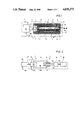
- FIG. 1 is a schematic sectional diagram of a mobile data carrier in the chute of the coupling station
- FIG. 2 is an equivalent circuit diagram for the data carrier and transmission unit
- FIG. 3 is a schematic sectional picture of a mobile data carrier metal encased by means of two half shells;
- FIG. 4 is an equivalent circuit diagram of the data carrier of FIG. 3 in the coupling station
- FIG. 5 is a schematic illustration of the appliance for transmission and storage of energy and information in spatially separate arrangement of the coupling station and the computer and operator module;
- FIG. 6 is a schematic illustration of an amplitude modulation for the combining of signal pulses and information in accordance with the principle of pulse modulation.
- FIG. 1 is a schematic illustration of an appliance for transmission and storage of energy and information in a mobile data carrier 1 designed in a card-shaped manner which is insertable into a chute-shaped transmission unit 2.
- the transmission unit 2 is designed as a capacitance effective coupling station 3. It consists of two surface electrodes 8, 9 spaced from each other and embedded in material layers 4, 5, 6, 7 having high relative dielectric constants. The space between the surface electrodes 8, 9 forms a chute 30 which has an aperture at one front face 32 of the coupling station 3, into which the card-shaped data carrier 1 is insertable.
- the surface electrodes 8, 9 of the coupling station 3 are arranged symmetrically with respect to each other.
- the mobile data carrier 1 consists, in the same way, of capacitively effective surface electrodes 10, 11 covered externally by material layers 14, 15 and 16 and spaced from each other, between which a circuit board 13 carrying electronic circuit elements 12 is arranged, the circuit board 13 being connected with the surface electrodes 10, 11 by means of lines 33, 34.
- the external material layers 14, 15, 16 of the data carrier 1 represent insulating surfaces with a high relative dielectric constant ⁇ r .
- the surface electrodes 10, 11 are arranged symmetrically with respect to each other with reference to the external shape of the data carrier 1. This measure imparts the property to the data carrier 1, that it is insertable into the chute-shaped transmission unit 2 independently of a predetermined utilization position, thus also, with the sides interchanged, and that it assures an unlimited ability to function.
- the flat electrodes 8 and 9 of the coupling stations 3 are connected through lines 17 and 18 with a driver circuit 19, which serves for making available an operational alternating voltage, which, on its part, causes generation of offset currents in the flat electrodes 8, 9 and 10, 11.
- a driver circuit 19 which serves for making available an operational alternating voltage, which, on its part, causes generation of offset currents in the flat electrodes 8, 9 and 10, 11.
- the differing magnitudes of the dielectric constants in the individual material layers 5, 14 and 6, 16 serve for the purpose of a desired increase of the offset currents in the arrangement of the coupling station 3 towards the data carrier during the energy coupling.
- a condenser is formed between the electrodes 10 and 11, thus the electrodes of the data carrier 1, in which all the elements, including the carrier substrate of the electronic circuit board 13, represent the dielectric of the condenser.
- This partial condenser is all the smaller thus less effective, the lower the relative dielectric constant ⁇ r .
- ⁇ r should be as large as possible for the material layers which are located between the electrodes 10 or 11 and 8 or 9 for the energy and information coupling.
- the offset currents are caused by an alternating voltage of high amplitude or high frequency, which is made available by the driver circuit 19.
- switching means 20 are provided which assure an extensively constant current behavior of the shifting current during a half phase of the driving operational alternating voltage. It is expedient in energy coupling to continuously offer an output, so that for the time period in which no output is available, for instance phase transitions of the alternating voltage/the alternating current, terminated differential processes, the energy storage units, so-called buffer condensers are as small as possible.
- a continuous output supply can be achieved by a suitably curved shape of the control voltage or by compensation of the reactive impedance 1/ ⁇ C ⁇ L, thus the series circuit of an inductive component.
- the inductive component can be achieved by suitable transformer-coupling circuits or by series circuits of a coil.
- a simultaneous input of energy and information into a data carrier 1 is, for instance, achieved by means of frequency modulation of the AC voltage from the driver circuit 19, whereby the AC voltage for the input of energy has a higher and independent frequency as compared to an average frequency for the input of information.
- a frequency modulation of the driving operational AC voltage from the driver circuit 19 in accordance with a return to zero code is utilized, (return to zero, constant voltage share-free coding).
- modulation depths of 10% to 100% are utilized for bit coding in such a way that a modulation expandable over 10% to 30% represents bit values of, for instance, "0", and a modulation expandable from 40% to 100% represents bit values of, for instance, "1".
- a linkage of signal pulse and information is performable, in such a way that a lowering 21 of the amplitude from 100% to 70% for the time period t 1 (see FIG.
- a lowering 22 of the amplitude by more than 70% represents the start of a "1"-bit
- the entire amplitude of the operational voltage of the driver circuit 19 for a time period t 2 represents a bit end 23.
- a simultaneous input of energy into the data carrier 1 and output of information from the data carrier 1 by means of changing the impedance in a receiving- and sending circuit 31 in the data carrier 1 is performable with the device in FIG. 1, in such a way that a bit-information, through changing and overlapping currents and/or voltages, is recognizable and evaluatable by the driver circuit 19.
- the evaluation can, for instance, occur by recognizing the AC voltage amplitudes between lines 17, 18 in the switching means 20 or by the resulting change in impedance, especially the reactive components (L, C). It is proposed, in a preferred embodiment, to perform the exchange of information between the data carrier 1 and the transmission unit 2 in the half-duplex mode.
- the transmission unit 2 consists of a coupling station 3 and the driver circuit 19.
- the flat electrodes 8 and 9 perform the function of coupling condensers and are connected with the driver circuit 19, 20 through the lines 17 and 18.
- the energy supply of the driver circuit 19, 20 occurs through a feed line 35.
- a signal connection 37 leads from the driver circuit 19 into a computer logic with an operator's module 36.
- Computer logic and operator modules 36 are also supplied with energy through a feed line 38.
- the flat electrodes 10 and 11 are part of coupling condensers in the data carrier 1 and are connected with the receiving and sending circuit 31 in the data carrier through lines 33 and 34.
- the receiving and sending circuit 31, as construction group, serves for the preparation and availability of the operational energy in the data carrier 1, for the demodulation of the information signals and finally for the modulation of the impedance at the flat electrodes 8,9 for the data output.
- a data processing unit 39 with memory (EEROM) and control logic is implemented in the mobile data carrier 1, which processing unit is connected with the receiving and sending circuit 31 through signal and feed connections 40.
- FIG. 3 shows an embodiment form of the mobile data carrier 1, which is embedded into capsule 24 insulated towards the outside and metal clad.
- the capsule 24 consists of two metal clad half shells 25 and 26 of conducting material, so that the offset currents for the inputting and outputting of energy information are transmittable by electrostatic induction at the flat electrodes 10, 11.
- the half shells 25, 26 are made of steel and are galvanically separated from each other by a circumferentially insulating separation layer 27.
- the outer casing of the metal clad mobile data carrier 1 consists also of insulating material layers 41, 42, 43.
- the data carrier 1 is structured in comparatively the same way as depicted in FIG. 1.
- FIG. 1 In the embodiment depicted in FIG.
- the structural elements of the data carrier 1 are placed in the inner space formed by the encapsulation 24. From top to bottom there are arranged the dielectric material 14, the flat electrode 10, the electronic circuit elements 12 on the printed circuit board 13 and possibly on a second printed circuit board 13/1, the flat electrode electode 11 and finally the dielectric material layer 16.
- FIG. 4 An equivalent circuit diagram of the data carrier 1 in FIG. 3 in the coupling station 3 is depicted in FIG. 4. According to this, respectively, outer condensers 44, 45 are formed between the flat electrodes 8, 9 in the coupling station 3 and the conducting half shell 25 or 26 and, respectively, inner condensers 46, 47 are formed between the conducting half shells 25 or 26 and the flat electrodes 10 or 11 in the data carrier 1.
- a complete encapsulation 24 of the data carrier 1 with a symmetrical construction assures a totally unproblematical handling of the data carrier 1, by providing functional ability of same in every possible insertion position. Because of the metal cladding of the data carrier 1 by embedding it in two half shells 25, 26 of steel plate any manipulative interventions are impossible without leaving traces of the damage or interference. In the metal clad embodiment of the data carrier 1 in FIG. 3, it is thus also impossible to access the flat electrodes 10 and 11 from the outside and to make changes of any sort by contacting any terminal.
Abstract
Description
Claims (18)
Applications Claiming Priority (2)
| Application Number | Priority Date | Filing Date | Title |
|---|---|---|---|
| DE3713251 | 1987-04-18 | ||
| DE3713251A DE3713251C2 (en) | 1987-04-18 | 1987-04-18 | Device for the transmission and storage of energy and information in a card-shaped, mobile data carrier |
Publications (1)
| Publication Number | Publication Date |
|---|---|
| US4835373A true US4835373A (en) | 1989-05-30 |
Family
ID=6325942
Family Applications (1)
| Application Number | Title | Priority Date | Filing Date |
|---|---|---|---|
| US07/182,952 Expired - Fee Related US4835373A (en) | 1987-04-18 | 1988-04-18 | Appliance for transmission and storage of energy and information in a card-shaped data carrier |
Country Status (6)
| Country | Link |
|---|---|
| US (1) | US4835373A (en) |
| EP (1) | EP0291685A3 (en) |
| JP (1) | JPS63280393A (en) |
| DE (1) | DE3713251C2 (en) |
| DK (1) | DK187988A (en) |
| PT (1) | PT87257A (en) |
Cited By (37)
| Publication number | Priority date | Publication date | Assignee | Title |
|---|---|---|---|---|
| US4931991A (en) * | 1988-12-22 | 1990-06-05 | Amp Incorporated | Machine readable memory card with capacitive interconnect |
| US5021767A (en) * | 1987-10-12 | 1991-06-04 | N.V. Nederlandsche Apparatenfabriek Nedap | Method and an apparatus for electronically identifying articles moving along a surface |
| US5204663A (en) * | 1990-05-21 | 1993-04-20 | Applied Systems Institute, Inc. | Smart card access control system |
| US5311003A (en) * | 1992-06-05 | 1994-05-10 | American Magnetics Corporation | Hand-operated magnetic stripe card reader |
| US5451763A (en) * | 1994-07-05 | 1995-09-19 | Alto Corporation | Personal medical IC card and read/write unit |
| WO1997028595A1 (en) * | 1996-01-16 | 1997-08-07 | Electro Dynamics, Inc. | Capacitive charge coupling with dual connector assemblies and charging system |
| DE19629086A1 (en) * | 1996-07-18 | 1998-01-29 | Siemens Ag | Portable data transmission device and fastener |
| EP0855064A1 (en) * | 1995-10-11 | 1998-07-29 | Motorola, Inc. | Remotely powered electronic tag and associated exciter/reader and related method |
| US5936841A (en) * | 1996-01-02 | 1999-08-10 | International Business Machines Corporation | PCMCIA RF connector |
| WO2000016289A1 (en) * | 1998-09-11 | 2000-03-23 | Motorola Inc. | Electrostatic rfid/eas system |
| EP1102207A2 (en) * | 1999-10-26 | 2001-05-23 | Philips Patentverwaltung GmbH | Label device |
| US6362972B1 (en) | 2000-04-13 | 2002-03-26 | Molex Incorporated | Contactless interconnection system |
| US6611199B1 (en) | 1995-10-11 | 2003-08-26 | Motorola, Inc. | Capacitively powered portable communication device and associated exciter/reader and related method |
| US6612852B1 (en) | 2000-04-13 | 2003-09-02 | Molex Incorporated | Contactless interconnection system |
| US20030189096A1 (en) * | 2002-04-08 | 2003-10-09 | Nokia Corporation | Mobile terminal featuring smart card interrupt |
| US20040140122A1 (en) * | 2001-05-17 | 2004-07-22 | Rainer Moll | Product comprising a substrate and a chip attached to the substrate |
| US20050178845A1 (en) * | 1998-12-09 | 2005-08-18 | Thierry Desfontaines | Contactless electronic communication device with optional auxiliary power source |
| US9433371B2 (en) | 2007-09-25 | 2016-09-06 | Proteus Digital Health, Inc. | In-body device with virtual dipole signal amplification |
| US9444503B2 (en) | 2006-11-20 | 2016-09-13 | Proteus Digital Health, Inc. | Active signal processing personal health signal receivers |
| US9603550B2 (en) | 2008-07-08 | 2017-03-28 | Proteus Digital Health, Inc. | State characterization based on multi-variate data fusion techniques |
| US9756874B2 (en) | 2011-07-11 | 2017-09-12 | Proteus Digital Health, Inc. | Masticable ingestible product and communication system therefor |
| US9883819B2 (en) | 2009-01-06 | 2018-02-06 | Proteus Digital Health, Inc. | Ingestion-related biofeedback and personalized medical therapy method and system |
| US9935487B2 (en) | 2013-12-05 | 2018-04-03 | Murata Manufacturing Co., Ltd. | Power receiving apparatus and power transmission system |
| US9941931B2 (en) | 2009-11-04 | 2018-04-10 | Proteus Digital Health, Inc. | System for supply chain management |
| US10084880B2 (en) | 2013-11-04 | 2018-09-25 | Proteus Digital Health, Inc. | Social media networking based on physiologic information |
| US10187121B2 (en) | 2016-07-22 | 2019-01-22 | Proteus Digital Health, Inc. | Electromagnetic sensing and detection of ingestible event markers |
| US10223905B2 (en) | 2011-07-21 | 2019-03-05 | Proteus Digital Health, Inc. | Mobile device and system for detection and communication of information received from an ingestible device |
| US10238604B2 (en) | 2006-10-25 | 2019-03-26 | Proteus Digital Health, Inc. | Controlled activation ingestible identifier |
| US10398161B2 (en) | 2014-01-21 | 2019-09-03 | Proteus Digital Heal Th, Inc. | Masticable ingestible product and communication system therefor |
| US10441194B2 (en) | 2007-02-01 | 2019-10-15 | Proteus Digital Heal Th, Inc. | Ingestible event marker systems |
| US10517506B2 (en) | 2007-05-24 | 2019-12-31 | Proteus Digital Health, Inc. | Low profile antenna for in body device |
| US10529044B2 (en) | 2010-05-19 | 2020-01-07 | Proteus Digital Health, Inc. | Tracking and delivery confirmation of pharmaceutical products |
| US10551218B2 (en) | 2014-05-23 | 2020-02-04 | Pragmatic Printing Limited | Capacitive detection, energy transfer, and/or data transfer system |
| US11464423B2 (en) | 2007-02-14 | 2022-10-11 | Otsuka Pharmaceutical Co., Ltd. | In-body power source having high surface area electrode |
| US11744481B2 (en) | 2013-03-15 | 2023-09-05 | Otsuka Pharmaceutical Co., Ltd. | System, apparatus and methods for data collection and assessing outcomes |
| US11928614B2 (en) | 2006-05-02 | 2024-03-12 | Otsuka Pharmaceutical Co., Ltd. | Patient customized therapeutic regimens |
| US11950615B2 (en) | 2021-11-10 | 2024-04-09 | Otsuka Pharmaceutical Co., Ltd. | Masticable ingestible product and communication system therefor |
Families Citing this family (8)
| Publication number | Priority date | Publication date | Assignee | Title |
|---|---|---|---|---|
| US4853523A (en) * | 1987-10-05 | 1989-08-01 | Pitney Bowes Inc. | Vault cartridge having capacitive coupling |
| JPH0390367U (en) * | 1989-12-30 | 1991-09-13 | ||
| JPH0478987A (en) * | 1990-07-20 | 1992-03-12 | Mitsubishi Electric Corp | Ic card |
| DE4036765A1 (en) * | 1990-11-17 | 1992-05-21 | Angewandte Digital Elektronik | CODED CHIP CARD ACTIVATION |
| DE4138131A1 (en) * | 1991-10-19 | 1993-04-22 | Provera Ges Fuer Projektierung | Non-contact chip card with integrated microprocessor - has read/write facility provided by optical capacitive or inductive coupling to card, and display powered by solar energy |
| DE4212111C2 (en) * | 1992-04-10 | 2003-05-22 | Angewandte Digital Elektronik | Indication of improperly treated chip cards |
| US5572441A (en) * | 1994-04-04 | 1996-11-05 | Lucent Technologies Inc. | Data connector for portable devices |
| JP5817365B2 (en) * | 2011-09-12 | 2015-11-18 | 大日本印刷株式会社 | Communication system, relay communication device, electromagnetic induction communication device, information storage medium |
Citations (1)
| Publication number | Priority date | Publication date | Assignee | Title |
|---|---|---|---|---|
| US4355300A (en) * | 1980-02-14 | 1982-10-19 | Coulter Systems Corporation | Indicia recognition apparatus |
Family Cites Families (5)
| Publication number | Priority date | Publication date | Assignee | Title |
|---|---|---|---|---|
| DE2252046A1 (en) * | 1972-10-24 | 1974-05-02 | Remvac Systems Corp | CARD WITH ENCRYPTED INFORMATION BITS AND ASSOCIATED READER |
| US4480178A (en) * | 1983-04-04 | 1984-10-30 | At&T Information Systems | Tuning arrangement for interfacing credit card-like device to a reader system |
| JPS59229686A (en) * | 1983-06-09 | 1984-12-24 | Toshiba Corp | Ic card |
| GB8328750D0 (en) * | 1983-10-27 | 1983-11-30 | Philp R | Contact-less electronic connectors |
| DE3630456A1 (en) * | 1986-09-06 | 1988-03-17 | Zeiss Ikon Ag | METHOD AND DEVICE FOR CONTACTLESS INFORMATION TRANSFER |
-
1987
- 1987-04-18 DE DE3713251A patent/DE3713251C2/en not_active Expired - Fee Related
-
1988
- 1988-04-07 DK DK187988A patent/DK187988A/en not_active Application Discontinuation
- 1988-04-12 EP EP88105763A patent/EP0291685A3/en not_active Withdrawn
- 1988-04-15 PT PT87257A patent/PT87257A/en unknown
- 1988-04-18 US US07/182,952 patent/US4835373A/en not_active Expired - Fee Related
- 1988-04-18 JP JP63093624A patent/JPS63280393A/en active Pending
Patent Citations (1)
| Publication number | Priority date | Publication date | Assignee | Title |
|---|---|---|---|---|
| US4355300A (en) * | 1980-02-14 | 1982-10-19 | Coulter Systems Corporation | Indicia recognition apparatus |
Cited By (51)
| Publication number | Priority date | Publication date | Assignee | Title |
|---|---|---|---|---|
| US5021767A (en) * | 1987-10-12 | 1991-06-04 | N.V. Nederlandsche Apparatenfabriek Nedap | Method and an apparatus for electronically identifying articles moving along a surface |
| US4931991A (en) * | 1988-12-22 | 1990-06-05 | Amp Incorporated | Machine readable memory card with capacitive interconnect |
| US5204663A (en) * | 1990-05-21 | 1993-04-20 | Applied Systems Institute, Inc. | Smart card access control system |
| US5311003A (en) * | 1992-06-05 | 1994-05-10 | American Magnetics Corporation | Hand-operated magnetic stripe card reader |
| US5451763A (en) * | 1994-07-05 | 1995-09-19 | Alto Corporation | Personal medical IC card and read/write unit |
| EP0855064A1 (en) * | 1995-10-11 | 1998-07-29 | Motorola, Inc. | Remotely powered electronic tag and associated exciter/reader and related method |
| US6611199B1 (en) | 1995-10-11 | 2003-08-26 | Motorola, Inc. | Capacitively powered portable communication device and associated exciter/reader and related method |
| EP0855064A4 (en) * | 1995-10-11 | 2001-07-18 | Motorola Inc | Remotely powered electronic tag and associated exciter/reader and related method |
| US5936841A (en) * | 1996-01-02 | 1999-08-10 | International Business Machines Corporation | PCMCIA RF connector |
| US5714864A (en) * | 1996-01-16 | 1998-02-03 | Electro Dynamics, Inc. | Capacitive charge coupling with dual connector assemblies and charging system |
| WO1997028595A1 (en) * | 1996-01-16 | 1997-08-07 | Electro Dynamics, Inc. | Capacitive charge coupling with dual connector assemblies and charging system |
| US6367701B1 (en) | 1996-07-18 | 2002-04-09 | Siemens Aktiengesellschaft | Portable data transmission device, and fixing element |
| KR100417041B1 (en) * | 1996-07-18 | 2004-02-05 | 지멘스 악티엔게젤샤프트 | Portable data transmission device and fastening element |
| DE19629086A1 (en) * | 1996-07-18 | 1998-01-29 | Siemens Ag | Portable data transmission device and fastener |
| WO2000016289A1 (en) * | 1998-09-11 | 2000-03-23 | Motorola Inc. | Electrostatic rfid/eas system |
| US9152906B2 (en) | 1998-12-09 | 2015-10-06 | Gemalto Sa | Contactless electronic communication device with optional auxiliary power source |
| US20050178845A1 (en) * | 1998-12-09 | 2005-08-18 | Thierry Desfontaines | Contactless electronic communication device with optional auxiliary power source |
| EP1102207A3 (en) * | 1999-10-26 | 2002-10-23 | Philips Corporate Intellectual Property GmbH | Label device |
| EP1102207A2 (en) * | 1999-10-26 | 2001-05-23 | Philips Patentverwaltung GmbH | Label device |
| US6362972B1 (en) | 2000-04-13 | 2002-03-26 | Molex Incorporated | Contactless interconnection system |
| US6612852B1 (en) | 2000-04-13 | 2003-09-02 | Molex Incorporated | Contactless interconnection system |
| US20040140122A1 (en) * | 2001-05-17 | 2004-07-22 | Rainer Moll | Product comprising a substrate and a chip attached to the substrate |
| US7344074B2 (en) | 2002-04-08 | 2008-03-18 | Nokia Corporation | Mobile terminal featuring smart card interrupt |
| WO2003085594A1 (en) * | 2002-04-08 | 2003-10-16 | Nokia Corporation | Mobile terminal featuring smart card interrupt |
| US20030189096A1 (en) * | 2002-04-08 | 2003-10-09 | Nokia Corporation | Mobile terminal featuring smart card interrupt |
| US11928614B2 (en) | 2006-05-02 | 2024-03-12 | Otsuka Pharmaceutical Co., Ltd. | Patient customized therapeutic regimens |
| US11357730B2 (en) | 2006-10-25 | 2022-06-14 | Otsuka Pharmaceutical Co., Ltd. | Controlled activation ingestible identifier |
| US10238604B2 (en) | 2006-10-25 | 2019-03-26 | Proteus Digital Health, Inc. | Controlled activation ingestible identifier |
| US9444503B2 (en) | 2006-11-20 | 2016-09-13 | Proteus Digital Health, Inc. | Active signal processing personal health signal receivers |
| US10441194B2 (en) | 2007-02-01 | 2019-10-15 | Proteus Digital Heal Th, Inc. | Ingestible event marker systems |
| US11464423B2 (en) | 2007-02-14 | 2022-10-11 | Otsuka Pharmaceutical Co., Ltd. | In-body power source having high surface area electrode |
| US10517506B2 (en) | 2007-05-24 | 2019-12-31 | Proteus Digital Health, Inc. | Low profile antenna for in body device |
| US9433371B2 (en) | 2007-09-25 | 2016-09-06 | Proteus Digital Health, Inc. | In-body device with virtual dipole signal amplification |
| US11217342B2 (en) | 2008-07-08 | 2022-01-04 | Otsuka Pharmaceutical Co., Ltd. | Ingestible event marker data framework |
| US10682071B2 (en) | 2008-07-08 | 2020-06-16 | Proteus Digital Health, Inc. | State characterization based on multi-variate data fusion techniques |
| US9603550B2 (en) | 2008-07-08 | 2017-03-28 | Proteus Digital Health, Inc. | State characterization based on multi-variate data fusion techniques |
| US9883819B2 (en) | 2009-01-06 | 2018-02-06 | Proteus Digital Health, Inc. | Ingestion-related biofeedback and personalized medical therapy method and system |
| US10305544B2 (en) | 2009-11-04 | 2019-05-28 | Proteus Digital Health, Inc. | System for supply chain management |
| US9941931B2 (en) | 2009-11-04 | 2018-04-10 | Proteus Digital Health, Inc. | System for supply chain management |
| US10529044B2 (en) | 2010-05-19 | 2020-01-07 | Proteus Digital Health, Inc. | Tracking and delivery confirmation of pharmaceutical products |
| US9756874B2 (en) | 2011-07-11 | 2017-09-12 | Proteus Digital Health, Inc. | Masticable ingestible product and communication system therefor |
| US10223905B2 (en) | 2011-07-21 | 2019-03-05 | Proteus Digital Health, Inc. | Mobile device and system for detection and communication of information received from an ingestible device |
| US11744481B2 (en) | 2013-03-15 | 2023-09-05 | Otsuka Pharmaceutical Co., Ltd. | System, apparatus and methods for data collection and assessing outcomes |
| US10084880B2 (en) | 2013-11-04 | 2018-09-25 | Proteus Digital Health, Inc. | Social media networking based on physiologic information |
| US9935487B2 (en) | 2013-12-05 | 2018-04-03 | Murata Manufacturing Co., Ltd. | Power receiving apparatus and power transmission system |
| US10398161B2 (en) | 2014-01-21 | 2019-09-03 | Proteus Digital Heal Th, Inc. | Masticable ingestible product and communication system therefor |
| US11255701B2 (en) | 2014-05-23 | 2022-02-22 | Pragmatic Printing Limited | Capacitive detection, energy transfer, and/or data transfer system |
| US10551218B2 (en) | 2014-05-23 | 2020-02-04 | Pragmatic Printing Limited | Capacitive detection, energy transfer, and/or data transfer system |
| US10797758B2 (en) | 2016-07-22 | 2020-10-06 | Proteus Digital Health, Inc. | Electromagnetic sensing and detection of ingestible event markers |
| US10187121B2 (en) | 2016-07-22 | 2019-01-22 | Proteus Digital Health, Inc. | Electromagnetic sensing and detection of ingestible event markers |
| US11950615B2 (en) | 2021-11-10 | 2024-04-09 | Otsuka Pharmaceutical Co., Ltd. | Masticable ingestible product and communication system therefor |
Also Published As
| Publication number | Publication date |
|---|---|
| JPS63280393A (en) | 1988-11-17 |
| DE3713251C2 (en) | 1996-04-11 |
| DK187988A (en) | 1988-10-19 |
| EP0291685A3 (en) | 1990-05-16 |
| PT87257A (en) | 1989-05-12 |
| DK187988D0 (en) | 1988-04-07 |
| EP0291685A2 (en) | 1988-11-23 |
| DE3713251A1 (en) | 1988-11-03 |
Similar Documents
| Publication | Publication Date | Title |
|---|---|---|
| US4835373A (en) | Appliance for transmission and storage of energy and information in a card-shaped data carrier | |
| EP0435137A2 (en) | Information card system | |
| CN101593285B (en) | Transponder, interrogator, and communication device | |
| US8130159B2 (en) | Electromagnetic field generation antenna for a transponder | |
| US9768836B2 (en) | Inductive energy supply unit | |
| US5293400A (en) | Contactless linking device for interconnecting data bus sections | |
| KR101150674B1 (en) | Data communication device | |
| US6825754B1 (en) | Radio frequency identification device for increasing tag activation distance and method thereof | |
| US5587578A (en) | Method and apparatus for optimizing magnetic flux through an electronic label of a contact-free identification system | |
| IN191477B (en) | ||
| KR19990008203A (en) | Contactless chip card | |
| CN103370834A (en) | Wireless communication device | |
| US9674972B2 (en) | Modular electronic system and bus subscriber | |
| CN108718117A (en) | A kind of constant double pickup three phase dynamic radio energy transmission systems of output voltage | |
| CA2233879A1 (en) | Ac current sensor | |
| JP2001501407A (en) | Wireless energy and data transmission for modular peripheral systems | |
| RU2029353C1 (en) | Touch-sensitive control panel for data input | |
| JPS61283981A (en) | Integrated circuit card | |
| JPH03209589A (en) | Transmitting / receiving system | |
| US5714744A (en) | Wave pickup in the form of a printed coil for an electronic portable object such as a no-contact card or badge | |
| EP0702316A1 (en) | Contactless data carrier system | |
| JP7154320B2 (en) | Systems for energy transfer and data exchange between electronic devices | |
| EP0469762A1 (en) | Reader unit | |
| ES8204193A1 (en) | Token reader. | |
| JP3230688B2 (en) | Contactless transfer method of data in semiconductor storage medium |
Legal Events
| Date | Code | Title | Description |
|---|---|---|---|
| AS | Assignment |
Owner name: MANNESMANN KIENZLE GMBH, POSTFACH 1640, D-7730 VIL Free format text: ASSIGNMENT OF ASSIGNORS INTEREST.;ASSIGNORS:ADAMS, JURGEN;LEMKE, MANFRED;REEL/FRAME:004952/0431 Effective date: 19880418 Owner name: MANNESMANN KIENZLE GMBH, POSTFACH 1640, D-7730 VIL Free format text: ASSIGNMENT OF ASSIGNORS INTEREST;ASSIGNORS:ADAMS, JURGEN;LEMKE, MANFRED;REEL/FRAME:004952/0431 Effective date: 19880418 |
|
| FEPP | Fee payment procedure |
Free format text: PAYOR NUMBER ASSIGNED (ORIGINAL EVENT CODE: ASPN); ENTITY STATUS OF PATENT OWNER: LARGE ENTITY |
|
| FPAY | Fee payment |
Year of fee payment: 4 |
|
| FPAY | Fee payment |
Year of fee payment: 8 |
|
| REMI | Maintenance fee reminder mailed | ||
| LAPS | Lapse for failure to pay maintenance fees | ||
| FP | Lapsed due to failure to pay maintenance fee |
Effective date: 20010530 |
|
| STCH | Information on status: patent discontinuation |
Free format text: PATENT EXPIRED DUE TO NONPAYMENT OF MAINTENANCE FEES UNDER 37 CFR 1.362 |