US4803392A - Piezoelectric transducer - Google Patents
Piezoelectric transducer Download PDFInfo
- Publication number
- US4803392A US4803392A US07/086,488 US8648887A US4803392A US 4803392 A US4803392 A US 4803392A US 8648887 A US8648887 A US 8648887A US 4803392 A US4803392 A US 4803392A
- Authority
- US
- United States
- Prior art keywords
- piezoelectric
- substrate
- thin film
- transducer according
- piezoelectric transducer
- Prior art date
- Legal status (The legal status is an assumption and is not a legal conclusion. Google has not performed a legal analysis and makes no representation as to the accuracy of the status listed.)
- Expired - Fee Related
Links
Images


Classifications
-
- H—ELECTRICITY
- H10—SEMICONDUCTOR DEVICES; ELECTRIC SOLID-STATE DEVICES NOT OTHERWISE PROVIDED FOR
- H10N—ELECTRIC SOLID-STATE DEVICES NOT OTHERWISE PROVIDED FOR
- H10N30/00—Piezoelectric or electrostrictive devices
- H10N30/1051—Piezoelectric or electrostrictive devices based on piezoelectric or electrostrictive films or coatings
- H10N30/10513—Piezoelectric or electrostrictive devices based on piezoelectric or electrostrictive films or coatings characterised by the underlying bases, e.g. substrates
-
- H—ELECTRICITY
- H10—SEMICONDUCTOR DEVICES; ELECTRIC SOLID-STATE DEVICES NOT OTHERWISE PROVIDED FOR
- H10N—ELECTRIC SOLID-STATE DEVICES NOT OTHERWISE PROVIDED FOR
- H10N30/00—Piezoelectric or electrostrictive devices
- H10N30/01—Manufacture or treatment
- H10N30/07—Forming of piezoelectric or electrostrictive parts or bodies on an electrical element or another base
- H10N30/074—Forming of piezoelectric or electrostrictive parts or bodies on an electrical element or another base by depositing piezoelectric or electrostrictive layers, e.g. aerosol or screen printing
- H10N30/076—Forming of piezoelectric or electrostrictive parts or bodies on an electrical element or another base by depositing piezoelectric or electrostrictive layers, e.g. aerosol or screen printing by vapour phase deposition
-
- H—ELECTRICITY
- H10—SEMICONDUCTOR DEVICES; ELECTRIC SOLID-STATE DEVICES NOT OTHERWISE PROVIDED FOR
- H10N—ELECTRIC SOLID-STATE DEVICES NOT OTHERWISE PROVIDED FOR
- H10N30/00—Piezoelectric or electrostrictive devices
- H10N30/30—Piezoelectric or electrostrictive devices with mechanical input and electrical output, e.g. functioning as generators or sensors
- H10N30/302—Sensors
Definitions
- the present invention relates to a transducer using a thin film of piezoelectric material and in particular to a transducer using a lead titanate (PbTiO 3 ) thin film having an excellent piezoelectric property.
- Lead titanate PbTiO 3 has a large crystal lattice anisotropy and a large spontaneous polarization Ps in the ferroelectric phase (in the tetragonal system). It also has a very large piezoelectricity and a very large pyroelectricity in the polarization axis (c-axis).
- a piezoelectric transducer using the lead titanate is disclosed in co-pending U.S. patent application Ser. No. 824,728 filed on Jan. 31, 1986 and entitled "Piezoelectric Transducer and process for its production".
- a thin film is formed by applying the sputtering method or the like to lead titanate PbTiO 3 , a polycrystalline film having random crystal axes is generated. Accordingly the property of lead titanate PbTiO that the piezoelectricity in the c-axis direction is large is not sufficiently achieved.
- a (100)-oriented platinum thin film is formed on a MgO single crystal substrate, and a c-axis oriented PbTiO 3 thin film is formed on this electrode as described in Japanese patent laid-open application JP-A-59-123285 (1984) or Journal of Applied Physics Vol. 60, No. 1, Pages 361-367 (1986).
- a c-axis oriented PbTiO 3 thin film is obtained. Since the Pt film is disposed as the intermediate layer, however, the property deterioration is inevitable as compared with the case where the PbTiO 3 thin film is formed directly on the single crystal substrate.
- An object of the present invention is to provide a piezoelectric transducer having such a structure that a piezoelectric thin film having excellent orientation can be formed and thereby a high effective sensitivity can be obtained.
- Another object of the present invention is to provide a piezoelectric transducer having a resonance frequency of 10 to 100 MHz which is hardly attainable with piezoelectric ceramics and having a high effective sensitivity.
- a piezoelectric transducer comprises a substrate made of a single crystal having a lattice constant substantially equal to that of a perovskite-type piezoelectric crystal, such as strontium titanate (SrTiO 3 ), magnesium oxide (MgO) or the like, a first electrode of a metal film formed on one of main surfaces of the substrate and having openings where the surface of the substrate is exposed, a piezoelectric thin film having a perovskite-type crystal structure so formed as to cover the first electrode and the openings, and a second electrode formed on the piezoelectric thin film.
- a perovskite-type piezoelectric crystal such as strontium titanate (SrTiO 3 ), magnesium oxide (MgO) or the like
- a first electrode of a metal film formed on one of main surfaces of the substrate and having openings where the surface of the substrate is exposed
- a piezoelectric thin film having a perovskite-type crystal structure so formed as to cover
- the above described piezoelectric thin film typically comprises lead titanate PbTiO 3 as the main component and is formed by the high frequency sputtering method.
- c-axis oriented crystals grow epitaxially at first.
- crystals oriented in the same direction as that of crystals of the opening are laminated with crystals of the opening taking as seeds.
- a piezoelectric film having c-axis orientation as a whole i.e., a piezoelectric film having high piezoelectricity and high pyroelectric property is obtained.
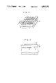
- FIG. 1A is a perspective view of an embodiment of the present invention.
- FIG. 1B is a sectional view along 1B--1B in
- FIG. 2A is a perspective view of another embodiment of the present invention.
- FIG. 2B is a sectional view along IIB--IIB in FIG. 2A
- FIG. 3 shows a plot of characteristics of the embodiment illustrated in FIG. 2A.
- FIGS. 4A and 5A are plane views of further embodiments of the present invention.
- FIGS. 4B and 5B are sectional views along IVB13 IVB in FIG. 4A and VB--VB in FIG. 5A, respectively.
- FIG. 6 is a perspective view of a further embodiment.
- FIG. 7 is a sectional view of a further embodiment.
- FIG. 1A shows a perspective view of a piezoelectric transducer according to the present invention
- FIG. 1B shows a sectional view along IB--IB in FIG. 1A.
- numeral 1 denotes a single crystal rod comprising strontium titanate.
- a number of linear and parallel grooves 2 having width of 1 ⁇ m and depth of approximately 100 nm are formed at intervals of approximately 1 ⁇ m.
- a first electrode comprising platinum is formed.
- a piezoelectric thin film 4 comprising lead titanate PbTiO 3 as the main component and having thickness of approximately 2 ⁇ m is formed.
- an upper electrode 5 comprising chrome and a gold film is disposed. All portions of the above described first electrodes 3 are externally connected in common.
- the grooves 2 may be disposed lengthwise and breadthwise and the electrodes 3 may be mutually connected inside the rod 1.
- a rod having a diameter of 10 mm and a length of 10 mm is made of (100)-oriented single crystal of strontium titanate and its one end face undergoes optical polishing. Then, a resist pattern is so formed on the end face by using the photolithography technique as to have lines of 1 ⁇ m in width and have spaces of 1 ⁇ m in width. By using ion milling with the resist taken as the mask, grooves 2 having depth of 100 nm are formed. After platinum films 3 have been deposited by using the evaporation method, the resist is removed. As a result, the electrode is so formed as to fill up the grooves 2.
- the lead titanate (PbTiO 3 ) thin film 4 is formed as the piezoelectric substance by rf-magnetron sputtering.
- the sputtering is performed under the condition that the temperature of the substrate, the pressure of Ar-O 2 gas (90 to 10%) and the thickness of the formed film are 600° C., 3 Pa and approximately 20 ⁇ m, respectively.
- Ar-O 2 gas 90 to 10%
- the thickness of the formed film are 600° C., 3 Pa and approximately 20 ⁇ m, respectively.
- strong peaks of (00l) appear, resulting in a c-axis oriented film.
- the letter l represents 1, 2 and 3.
- chrome (Cr) and gold (Au) are vapor-deposited to form the upper electrode. While keeping the temperature of the sample at 150° C., direct current voltage of 100 KV/cm is applied between both electrodes for 10 minutes to perform the polarization processing.
- the sensitivity of the piezoelectric transducer fabricated by the above described method was measured by using the pulse echo method. That is to say, electrical burst waves were applied between both electrodes to produce ultrasonic waves.
- the intensity of the echo reflected by the other end face of cylindrical strontium titanate was measured in the frequency range of 0.1 to 1.2 GHz.
- the electromechanical coupling coefficient calculated from the resultant frequency characteristics was 0.6. This value is larger than the value (0.50) of ceramics, the effect of c-axis orientation of lead titanate being indicated.
- a lead titanate thin film is formed by the rf-magnetron sputtering method.
- the sputtering is performed under the condition that the pressure of the introduced gas (Ar: 90%, O 2 : 10%) and the temperature of the substrate are 3 Pa and 200° C., respectively.
- the pressure of the introduced gas Ar: 90%, O 2 : 10%
- the temperature of the substrate 3 Pa and 200° C., respectively.
- significant diffraction lines do not appear, indicating that the film is amorphous.
- Its heat treatment at 600° C. for 8 hours generated strong diffraction lines of (00l) and weak diffraction lines of (h00). It was thus found that the heat treatment caused c-axis oriented crystallization
- This method provides a lead titanate thin film which is excellent in crystalline property as compared with the case of high temperature sputtering. If the film thickness is increased, however, polycrystallization is caused. At first, therefore, an amorphous thin film undergoes heat treatment to be transformed into a single crystal. Thereafter, sputtering is performed until a desired thin film is obtained while keeping the substrate at a high temperature.
- a piezoelectric transducer was actually formed by this method.
- a lead titanate thin film with thickness of 300 nm was formed as an amorphous film at first.
- the lead titanate thin film underwent heat treatment at 600° C. for 8 hours to be transformed into a single crystal Thereafter, sputtering was performed at substrate temperature of 550° C. for 10 hours to form a lead titanate thin film with thickness of approximately 3 ⁇ m.
- very strong diffraction lines of (00l) and weak diffraction lines of (h00) appeared.
- the top electrode 5 was formed and polarization processing was performed.
- the sensitivity of the transducer was estimated. The 0.65. By using this method, a transducer having a higher sensitivity can be formed.
- FIGS. 2A and 2B show a piezoelectric transducer using composite resonance which can be fabricated in the same way as the piezoelectric transducer illustrated in FIGS. 1A and 1B.
- a single crystal plate having thickness of 0.1 mm and diameter of 3 mm and comprising strontium titanate is used as a substrate 1'. Both faces of this single crystal plate are optically polished.
- Other reference numerals denote the same components as those of FIGS. 1A and 1B having the same numerals.
- a piezoelectric transducer using such a thin single-crystal substrate is able to have resonance frequencies which can be obtained neither in thin film piezoelectric transducers nor in transducers using conventional piezoelectric ceramics.
- FIG. 3 shows measurements of effective coupling coefficients of a composite resonator with respect to the first to fourth modes. At the second mode, the value of keff exceeds 0.4, resulting in a practical sensitivity.
- the single crystal substrate comprises strontium titanate.
- other single crystal substrates comprising magnesium oxide (MgO) or the like capable of epitaxially growing lead titanate may be used.
- the electrode material a metal withstanding a temperature close to 600° C. such as palladium (Pd), iridium (Ir), rhodium (Rh) or tungsten (W) may be used.
- FIGS. 4A and 4B are a plane view and a sectional view of a further embodiment, respectively.
- This embodiment is an array-type piezoelectric transducer.
- a substrate 11 comprising a single crystal plate of strontium titanate
- grooves 12 are disposed at constant intervals in the region corresponding to the transducer device.
- the original substrate surface 16 remains in a stripe form.
- the substrate surface is shaved by ion milling to the same depth as that of the above described grooves 12.
- Platinum is embedded in the grooves 12.
- platinum is also formed in the separation regions 18 and the peripheral regions 19 to form a lower electrode 13.
- a lead titanate thin film 14 is laminated. Further, portions of an upper electrode 15 are formed for respective transducer regions.
- FIGS. 5A and 5B are a plane view and a sectional view of an arrayed transducer using composite resonance.
- the transducer illustrated in FIGS. 5A and 5B differs from that illustrated in FIGS. 4A and 4B in that a substrate 11 comprising a strontium titanate single crystal and a lead titanate thin film 14 are also divided into portions corresponding to respective elements. These divided elements are arranged on a backing material 20.
- This structure is obtained by successively etching an upper electrode 15, a lead titanate thin film 14 and a strontium titanate substrate 11 by means of reactive ion etching.
- FIG. 7 is a sectional view of an embodiment having no embedded electrodes.
- numeral 1 denotes a single crystal substrate comprising strontium titanate or the like
- numeral 3' a first electrode formed on the substrate in a stripe form
- numeral 30 an opening where the substrate is exposed
- numeral 4 a thin film comprising lead titanate as the main component
- numeral 5 denotes an upper electrode.
- electrode platinum was vapor-deposited to form thickness of approximately 50 nm. Further, a resist pattern comprising lines having thickness of 1 ⁇ m and spaces having thickness of 1 ⁇ m was formed by a photolithography method. At first, the platinum film was etched by using freon CF 4 gas and reactive ion etching. Subsequently in oxygen plasma, the resist was removed to form a pattern 3' of a platinum film.
- the platinum film pattern can also be made by the lift-off method, i.e., by vapor-depositing a Pt film on a preformed resist pattern and thereafter removing the resist Subsequently, a thin film having thickness of 150 nm and comprising lead titanate as the main component was formed by the rf-magnetron sputtering method.
- the thin film was made under the condition that the substrate temperature was 200° C. and the pressure of the introduced gas (Ar: 90%, 0 2 : 10%) was 4 Pa. As a result of estimation of this film by using x-ray diffraction, the diffraction peak did not appear. It was thus found that this film was amorphous.
- this film underwent heat treatment and crystallization and thereafter underwent estimation using x-ray diffraction again.
- a lead titanate thin film was so formed as to have thickness of approximately 3 ⁇ m by rf sputtering under the condition that the substrate temperature was 550° C. and the gas pressure was 4 Pa in the same way as the preceding step.
- intensities of (001), (002) and (003) increased and other diffraction lines did not appear.
- a spotlike pattern appeared. It was thus confirmed that a uniformly oriented film was obtained.
- chrome (Cr) and gold (Au) were vapor-deposited to form an upper electrode by using a mask of 5 mm ⁇ . While keeping the temperature of the sample at 200° C., direct current voltage of 100 KV/cm was applied between both electrodes for 20 minutes to perform polarization processings. The intensity of the echo reflected by the other end face of the cylindrical strontium titanate was measured in the frequency range of 0.1 to 0.2 GHz. The electromechanical coupling coefficient calculated from the resultant frequency characteristics was 0.65. It exceeds the value 0.5 of the coupling coefficient of lead titanate ceramics. It is considered that the effect of forming a c-axis oriented film on the platinum electrode as well by lateral epitaxis has been obtained.
- a thin film having a desired film thickness may be formed by forming a lead titanate thin film to such a degree that the electrode is covered and thereafter repeating steps for forming an amorphous film having appropriate thickness and for applying heat treatment.
Abstract
Description
Claims (18)
Applications Claiming Priority (2)
| Application Number | Priority Date | Filing Date | Title |
|---|---|---|---|
| JP61225935A JPS6382100A (en) | 1986-09-26 | 1986-09-26 | Piezoelectric element and its manufacture |
| JP61-225935 | 1986-09-26 |
Publications (1)
| Publication Number | Publication Date |
|---|---|
| US4803392A true US4803392A (en) | 1989-02-07 |
Family
ID=16837200
Family Applications (1)
| Application Number | Title | Priority Date | Filing Date |
|---|---|---|---|
| US07/086,488 Expired - Fee Related US4803392A (en) | 1986-09-26 | 1987-08-18 | Piezoelectric transducer |
Country Status (2)
| Country | Link |
|---|---|
| US (1) | US4803392A (en) |
| JP (1) | JPS6382100A (en) |
Cited By (20)
| Publication number | Priority date | Publication date | Assignee | Title |
|---|---|---|---|---|
| US5065068A (en) * | 1989-06-07 | 1991-11-12 | Oakley Clyde G | Ferroelectric ceramic transducer |
| US5101133A (en) * | 1990-01-09 | 1992-03-31 | Richard Wolf Gmbh | Ultrasonic transducer having piezoelectric transducer elements |
| US5569547A (en) * | 1993-10-08 | 1996-10-29 | Ube Industries, Ltd. | Ceramic composite material |
| US5759753A (en) * | 1995-07-19 | 1998-06-02 | Matsushita Electric Industrial Co., Ltd. | Piezoelectric device and method of manufacturing the same |
| US5866238A (en) * | 1994-05-05 | 1999-02-02 | Minolta Co., Ltd. | Ferroelectric thin film device and its process |
| US6271620B1 (en) * | 1999-05-20 | 2001-08-07 | Sen Corporation | Acoustic transducer and method of making the same |
| US6438070B1 (en) | 1999-10-04 | 2002-08-20 | Halliburton Energy Services, Inc. | Hydrophone for use in a downhole tool |
| US20040021397A1 (en) * | 2002-02-04 | 2004-02-05 | Oakland University | Magnetoelectric effects of magnetostrictive and piezoelectric layered composites |
| US20050134148A1 (en) * | 2003-12-18 | 2005-06-23 | Palo Alto Research Center Incorporated. | Broad frequency band energy scavenger |
| US20060130476A1 (en) * | 2004-12-20 | 2006-06-22 | Palo Alto Research Center Incorporated | Energy scavengers which adjust their frequency by altering liquid distributions on a beam |
| US20070038111A1 (en) * | 2005-08-12 | 2007-02-15 | Scimed Life Systems, Inc. | Micromachined imaging transducer |
| US20090108708A1 (en) * | 2007-10-26 | 2009-04-30 | Trs Technologies, Inc. | Micromachined piezoelectric ultrasound transducer arrays |
| US9224938B2 (en) | 2011-04-11 | 2015-12-29 | Halliburton Energy Services, Inc. | Piezoelectric element and method to remove extraneous vibration modes |
| US9664783B2 (en) | 2014-07-15 | 2017-05-30 | Garmin Switzerland Gmbh | Marine sonar display device with operating mode determination |
| US9766328B2 (en) | 2014-07-15 | 2017-09-19 | Garmin Switzerland Gmbh | Sonar transducer array assembly and methods of manufacture thereof |
| US9784825B2 (en) | 2014-07-15 | 2017-10-10 | Garmin Switzerland Gmbh | Marine sonar display device with cursor plane |
| US9784826B2 (en) | 2014-07-15 | 2017-10-10 | Garmin Switzerland Gmbh | Marine multibeam sonar device |
| US9812118B2 (en) | 2014-07-15 | 2017-11-07 | Garmin Switzerland Gmbh | Marine multibeam sonar device |
| US10514451B2 (en) | 2014-07-15 | 2019-12-24 | Garmin Switzerland Gmbh | Marine sonar display device with three-dimensional views |
| US10605913B2 (en) | 2015-10-29 | 2020-03-31 | Garmin Switzerland Gmbh | Sonar noise interference rejection |
Citations (6)
| Publication number | Priority date | Publication date | Assignee | Title |
|---|---|---|---|---|
| US3688222A (en) * | 1971-03-18 | 1972-08-29 | Us Army | Matched ultrasonic delay line with solderable transducer electrodes |
| US4117074A (en) * | 1976-08-30 | 1978-09-26 | Tiersten Harry F | Monolithic mosaic piezoelectric transducer utilizing trapped energy modes |
| US4236095A (en) * | 1978-04-18 | 1980-11-25 | Matsushita Electric Industrial Company, Limited | Surface acoustic wave device comprising piezoelectric substrate having zinc oxide layer on α-alumina layer |
| US4484098A (en) * | 1983-12-19 | 1984-11-20 | United Technologies Corporation | Environmentally stable lithium niobate acoustic wave devices |
| US4511816A (en) * | 1982-03-11 | 1985-04-16 | Nobuo Mikoshiba | Surface acoustic wave device using an elastic substrate and an aluminum nitride piezoelectric film |
| US4567393A (en) * | 1983-06-14 | 1986-01-28 | Clarion Co., Ltd. | Surface acoustic wave device having AlN and ZnO layers on a Si substrate |
-
1986
- 1986-09-26 JP JP61225935A patent/JPS6382100A/en active Pending
-
1987
- 1987-08-18 US US07/086,488 patent/US4803392A/en not_active Expired - Fee Related
Patent Citations (6)
| Publication number | Priority date | Publication date | Assignee | Title |
|---|---|---|---|---|
| US3688222A (en) * | 1971-03-18 | 1972-08-29 | Us Army | Matched ultrasonic delay line with solderable transducer electrodes |
| US4117074A (en) * | 1976-08-30 | 1978-09-26 | Tiersten Harry F | Monolithic mosaic piezoelectric transducer utilizing trapped energy modes |
| US4236095A (en) * | 1978-04-18 | 1980-11-25 | Matsushita Electric Industrial Company, Limited | Surface acoustic wave device comprising piezoelectric substrate having zinc oxide layer on α-alumina layer |
| US4511816A (en) * | 1982-03-11 | 1985-04-16 | Nobuo Mikoshiba | Surface acoustic wave device using an elastic substrate and an aluminum nitride piezoelectric film |
| US4567393A (en) * | 1983-06-14 | 1986-01-28 | Clarion Co., Ltd. | Surface acoustic wave device having AlN and ZnO layers on a Si substrate |
| US4484098A (en) * | 1983-12-19 | 1984-11-20 | United Technologies Corporation | Environmentally stable lithium niobate acoustic wave devices |
Cited By (32)
| Publication number | Priority date | Publication date | Assignee | Title |
|---|---|---|---|---|
| US5065068A (en) * | 1989-06-07 | 1991-11-12 | Oakley Clyde G | Ferroelectric ceramic transducer |
| US5101133A (en) * | 1990-01-09 | 1992-03-31 | Richard Wolf Gmbh | Ultrasonic transducer having piezoelectric transducer elements |
| US5569547A (en) * | 1993-10-08 | 1996-10-29 | Ube Industries, Ltd. | Ceramic composite material |
| US5866238A (en) * | 1994-05-05 | 1999-02-02 | Minolta Co., Ltd. | Ferroelectric thin film device and its process |
| US5759753A (en) * | 1995-07-19 | 1998-06-02 | Matsushita Electric Industrial Co., Ltd. | Piezoelectric device and method of manufacturing the same |
| US5982010A (en) * | 1995-07-19 | 1999-11-09 | Matsushita Electric Industrial Co., Ltd. | Piezoelectric device and method of manufacturing the same |
| US6271620B1 (en) * | 1999-05-20 | 2001-08-07 | Sen Corporation | Acoustic transducer and method of making the same |
| US6438070B1 (en) | 1999-10-04 | 2002-08-20 | Halliburton Energy Services, Inc. | Hydrophone for use in a downhole tool |
| US6594199B2 (en) | 1999-10-04 | 2003-07-15 | Halliburton Energy Services, Inc. | Hydrophone for use in a downhole tool |
| US20040021397A1 (en) * | 2002-02-04 | 2004-02-05 | Oakland University | Magnetoelectric effects of magnetostrictive and piezoelectric layered composites |
| US7226666B2 (en) * | 2002-02-04 | 2007-06-05 | Oakland University | Magnetoelectric effects of magnetostrictive and piezoelectric layered composites |
| US20050134148A1 (en) * | 2003-12-18 | 2005-06-23 | Palo Alto Research Center Incorporated. | Broad frequency band energy scavenger |
| US7057330B2 (en) | 2003-12-18 | 2006-06-06 | Palo Alto Research Center Incorporated | Broad frequency band energy scavenger |
| US20060130476A1 (en) * | 2004-12-20 | 2006-06-22 | Palo Alto Research Center Incorporated | Energy scavengers which adjust their frequency by altering liquid distributions on a beam |
| US7293411B2 (en) | 2004-12-20 | 2007-11-13 | Palo Alto Research Center Incorporated | Energy scavengers which adjust their frequency by altering liquid distributions on a beam |
| US20090029295A1 (en) * | 2005-08-12 | 2009-01-29 | Rehrig Paul W | Micromachined imaging transducer |
| US20070038111A1 (en) * | 2005-08-12 | 2007-02-15 | Scimed Life Systems, Inc. | Micromachined imaging transducer |
| US7622853B2 (en) * | 2005-08-12 | 2009-11-24 | Scimed Life Systems, Inc. | Micromachined imaging transducer |
| US20090108708A1 (en) * | 2007-10-26 | 2009-04-30 | Trs Technologies, Inc. | Micromachined piezoelectric ultrasound transducer arrays |
| US20110191997A1 (en) * | 2007-10-26 | 2011-08-11 | Trs Technologies, Inc. | Micromachined piezoelectric ultrasound transducer arrays |
| US8008842B2 (en) | 2007-10-26 | 2011-08-30 | Trs Technologies, Inc. | Micromachined piezoelectric ultrasound transducer arrays |
| US20110215677A1 (en) * | 2007-10-26 | 2011-09-08 | Trs Technologies, Inc. | Micromachined piezoelectric ultrasound transducer arrays |
| US8148877B2 (en) | 2007-10-26 | 2012-04-03 | Trs Technologies, Inc. | Micromachined piezoelectric ultrasound transducer arrays |
| US9224938B2 (en) | 2011-04-11 | 2015-12-29 | Halliburton Energy Services, Inc. | Piezoelectric element and method to remove extraneous vibration modes |
| US9664783B2 (en) | 2014-07-15 | 2017-05-30 | Garmin Switzerland Gmbh | Marine sonar display device with operating mode determination |
| US9766328B2 (en) | 2014-07-15 | 2017-09-19 | Garmin Switzerland Gmbh | Sonar transducer array assembly and methods of manufacture thereof |
| US9784825B2 (en) | 2014-07-15 | 2017-10-10 | Garmin Switzerland Gmbh | Marine sonar display device with cursor plane |
| US9784826B2 (en) | 2014-07-15 | 2017-10-10 | Garmin Switzerland Gmbh | Marine multibeam sonar device |
| US9812118B2 (en) | 2014-07-15 | 2017-11-07 | Garmin Switzerland Gmbh | Marine multibeam sonar device |
| US10514451B2 (en) | 2014-07-15 | 2019-12-24 | Garmin Switzerland Gmbh | Marine sonar display device with three-dimensional views |
| US11204416B2 (en) | 2014-07-15 | 2021-12-21 | Garmin Switzerland Gmbh | Marine multibeam sonar device |
| US10605913B2 (en) | 2015-10-29 | 2020-03-31 | Garmin Switzerland Gmbh | Sonar noise interference rejection |
Also Published As
| Publication number | Publication date |
|---|---|
| JPS6382100A (en) | 1988-04-12 |
Similar Documents
| Publication | Publication Date | Title |
|---|---|---|
| US4803392A (en) | Piezoelectric transducer | |
| US6709776B2 (en) | Multilayer thin film and its fabrication process as well as electron device | |
| US4640756A (en) | Method of making a piezoelectric shear wave resonator | |
| US4719383A (en) | Piezoelectric shear wave resonator and method of making same | |
| KR100671375B1 (en) | Thin film multilayer body, electronic device using such thin film multilayer body, actuator, and method for manufacturing actuator | |
| US20040155559A1 (en) | Ferroelectric thin film element, piezoelectric actuator and liquid discharge head | |
| Kushida et al. | Piezoelectricity of c‐axis oriented PbTiO3 thin films | |
| US20020006733A1 (en) | Multilayer thin film and its fabrication process as well as electron device | |
| KR100827216B1 (en) | Microelectronic piezoelectric structure | |
| JPS61177900A (en) | Piezo-electric element and its manufacture | |
| JP2532381B2 (en) | Ferroelectric thin film element and manufacturing method thereof | |
| Shih et al. | Theoretical investigation of the SAW properties of ferroelectric film composite structures | |
| JP2001077438A (en) | Piezoelectric element, ink-jet recorder head and manufacture thereof | |
| JP2002029894A (en) | Laminated thin film, method of producing the same and electronic device | |
| Kushida et al. | Ferroelectric properties of c-axis oriented PbTiO3 films Thin films, surfaces, and small particles | |
| US6482538B2 (en) | Microelectronic piezoelectric structure and method of forming the same | |
| KR100738852B1 (en) | Semiconductor memory element and ultrasonic sensor | |
| JPH08186182A (en) | Ferroelectric thin-film element | |
| Bao et al. | Microstructure and ferroelectric properties of low-fatigue epitaxial, all (001)-oriented (Bi, La) 4Ti3O12∕ Pb (Zr0. 4Ti0. 6) O3∕(Bi, La) 4Ti3O12 trilayered thin films on (001) SrTiO3 substrates | |
| JP3482048B2 (en) | Thin film infrared sensor | |
| JPH0548642B2 (en) | ||
| JPH0576793B2 (en) | ||
| US20040106014A1 (en) | Microwave tunable device having ferroelectric/dielectric BST film | |
| JP2568505B2 (en) | Ferroelectric thin film element | |
| JPS62100099A (en) | Piezoelectric element and its manufacture |
Legal Events
| Date | Code | Title | Description |
|---|---|---|---|
| AS | Assignment |
Owner name: HITACHI, LTD., 6, KANDA SURUGADAI 4-CHOME, CHIYODA Free format text: ASSIGNMENT OF ASSIGNORS INTEREST.;ASSIGNORS:KUSHIDA, KEIKO;TAKEUCHI, HIROSHI;KOBAYASHI, TOSHIO;AND OTHERS;REEL/FRAME:004774/0510 Effective date: 19870806 Owner name: HITACHI, LTD.,JAPAN Free format text: ASSIGNMENT OF ASSIGNORS INTEREST;ASSIGNORS:KUSHIDA, KEIKO;TAKEUCHI, HIROSHI;KOBAYASHI, TOSHIO;AND OTHERS;REEL/FRAME:004774/0510 Effective date: 19870806 |
|
| FPAY | Fee payment |
Year of fee payment: 4 |
|
| FEPP | Fee payment procedure |
Free format text: PAYOR NUMBER ASSIGNED (ORIGINAL EVENT CODE: ASPN); ENTITY STATUS OF PATENT OWNER: LARGE ENTITY |
|
| FPAY | Fee payment |
Year of fee payment: 8 |
|
| REMI | Maintenance fee reminder mailed | ||
| LAPS | Lapse for failure to pay maintenance fees | ||
| FP | Lapsed due to failure to pay maintenance fee |
Effective date: 20010207 |
|
| STCH | Information on status: patent discontinuation |
Free format text: PATENT EXPIRED DUE TO NONPAYMENT OF MAINTENANCE FEES UNDER 37 CFR 1.362 |