US4802178A - High speed fiberoptic laser module - Google Patents
High speed fiberoptic laser module Download PDFInfo
- Publication number
- US4802178A US4802178A US06/849,960 US84996086A US4802178A US 4802178 A US4802178 A US 4802178A US 84996086 A US84996086 A US 84996086A US 4802178 A US4802178 A US 4802178A
- Authority
- US
- United States
- Prior art keywords
- laser
- substrate
- module
- recited
- housing
- Prior art date
- Legal status (The legal status is an assumption and is not a legal conclusion. Google has not performed a legal analysis and makes no representation as to the accuracy of the status listed.)
- Expired - Lifetime
Links
Images

Classifications
-
- H—ELECTRICITY
- H01—ELECTRIC ELEMENTS
- H01S—DEVICES USING THE PROCESS OF LIGHT AMPLIFICATION BY STIMULATED EMISSION OF RADIATION [LASER] TO AMPLIFY OR GENERATE LIGHT; DEVICES USING STIMULATED EMISSION OF ELECTROMAGNETIC RADIATION IN WAVE RANGES OTHER THAN OPTICAL
- H01S5/00—Semiconductor lasers
- H01S5/02—Structural details or components not essential to laser action
- H01S5/024—Arrangements for thermal management
- H01S5/02407—Active cooling, e.g. the laser temperature is controlled by a thermo-electric cooler or water cooling
- H01S5/02415—Active cooling, e.g. the laser temperature is controlled by a thermo-electric cooler or water cooling by using a thermo-electric cooler [TEC], e.g. Peltier element
-
- G—PHYSICS
- G02—OPTICS
- G02B—OPTICAL ELEMENTS, SYSTEMS OR APPARATUS
- G02B6/00—Light guides; Structural details of arrangements comprising light guides and other optical elements, e.g. couplings
- G02B6/24—Coupling light guides
- G02B6/42—Coupling light guides with opto-electronic elements
- G02B6/4201—Packages, e.g. shape, construction, internal or external details
- G02B6/4202—Packages, e.g. shape, construction, internal or external details for coupling an active element with fibres without intermediate optical elements, e.g. fibres with plane ends, fibres with shaped ends, bundles
-
- G—PHYSICS
- G02—OPTICS
- G02B—OPTICAL ELEMENTS, SYSTEMS OR APPARATUS
- G02B6/00—Light guides; Structural details of arrangements comprising light guides and other optical elements, e.g. couplings
- G02B6/24—Coupling light guides
- G02B6/42—Coupling light guides with opto-electronic elements
- G02B6/4201—Packages, e.g. shape, construction, internal or external details
- G02B6/4248—Feed-through connections for the hermetical passage of fibres through a package wall
-
- H—ELECTRICITY
- H01—ELECTRIC ELEMENTS
- H01S—DEVICES USING THE PROCESS OF LIGHT AMPLIFICATION BY STIMULATED EMISSION OF RADIATION [LASER] TO AMPLIFY OR GENERATE LIGHT; DEVICES USING STIMULATED EMISSION OF ELECTROMAGNETIC RADIATION IN WAVE RANGES OTHER THAN OPTICAL
- H01S5/00—Semiconductor lasers
- H01S5/02—Structural details or components not essential to laser action
- H01S5/022—Mountings; Housings
- H01S5/0225—Out-coupling of light
- H01S5/02251—Out-coupling of light using optical fibres
-
- H—ELECTRICITY
- H01—ELECTRIC ELEMENTS
- H01S—DEVICES USING THE PROCESS OF LIGHT AMPLIFICATION BY STIMULATED EMISSION OF RADIATION [LASER] TO AMPLIFY OR GENERATE LIGHT; DEVICES USING STIMULATED EMISSION OF ELECTROMAGNETIC RADIATION IN WAVE RANGES OTHER THAN OPTICAL
- H01S5/00—Semiconductor lasers
- H01S5/02—Structural details or components not essential to laser action
- H01S5/022—Mountings; Housings
- H01S5/0235—Method for mounting laser chips
- H01S5/02355—Fixing laser chips on mounts
- H01S5/0237—Fixing laser chips on mounts by soldering
-
- H—ELECTRICITY
- H01—ELECTRIC ELEMENTS
- H01S—DEVICES USING THE PROCESS OF LIGHT AMPLIFICATION BY STIMULATED EMISSION OF RADIATION [LASER] TO AMPLIFY OR GENERATE LIGHT; DEVICES USING STIMULATED EMISSION OF ELECTROMAGNETIC RADIATION IN WAVE RANGES OTHER THAN OPTICAL
- H01S5/00—Semiconductor lasers
- H01S5/02—Structural details or components not essential to laser action
- H01S5/024—Arrangements for thermal management
- H01S5/02438—Characterized by cooling of elements other than the laser chip, e.g. an optical element being part of an external cavity or a collimating lens
-
- Y—GENERAL TAGGING OF NEW TECHNOLOGICAL DEVELOPMENTS; GENERAL TAGGING OF CROSS-SECTIONAL TECHNOLOGIES SPANNING OVER SEVERAL SECTIONS OF THE IPC; TECHNICAL SUBJECTS COVERED BY FORMER USPC CROSS-REFERENCE ART COLLECTIONS [XRACs] AND DIGESTS
- Y10—TECHNICAL SUBJECTS COVERED BY FORMER USPC
- Y10S—TECHNICAL SUBJECTS COVERED BY FORMER USPC CROSS-REFERENCE ART COLLECTIONS [XRACs] AND DIGESTS
- Y10S257/00—Active solid-state devices, e.g. transistors, solid-state diodes
- Y10S257/93—Thermoelectric, e.g. peltier effect cooling
Definitions
- This invention concerns a tiny module for receiving a microwave frequency signal which modulates a laser for transmitting a high frequency optical signal.
- a high speed laser control device which will apply modulated signals to a semiconductor laser diode for producing optical signals.
- Such a device should be rugged and self contained for practical utilization. It should accept signals at frequencies into the microwave range and couple them efficiently without interference to the laser diode.
- the device should exhibit a characteristic impedance of fifty ohms to match the impedance of a variety of conventional signal sources. It is desirable that the device be hermetically sealed for enhanced reliability in various environmental conditions.
- Such a device should be readily controllable, preferably with self-contained diagnostic sensors. It is preferably small and has low power consumption so that heat generation problems are minimized. It is also desirable that such a device be economically manufactured.
- a semiconductor laser module in a sealed metal housing A semiconductor laser diode is mounted on a laser substrate with an optical fiber connected to the substrate in alignment with the laser for receiving an output signal.
- a separate microwave signal connection substrate is also contained in the housing.
- a microwave lead on this latter substrate is coupled to a pin of an external connector for application of a microwave signal from an external source.
- a laser bias circuit is placed on the signal substrate and is connected to the microwave lead by an impedance matching connection. One terminal of the laser diode is connected to the bias circuit and the other terminal is connected to ground.
- the laser substrate is mounted on a thermoelectric cooler for temperature control.
- a thermistor on the substrate senses its temperature. It is also desirable to mount a photodiode in the module for sensing light from the laser for control of its performance.
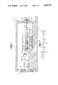
- FIG. 1 is a transverse cross section of a laser communication module constructed according to principles of this invention
- FIG. 2 is a plan view of the module with the cover removed to show the interior
- FIG. 3 is a circuit diagram of the electrical drive for the laser diode in the module.
- the laser module is hermetically sealed in a grounded metal housing formed of a base 10, a rectangular ring or frame 11 forming the walls of the housing, and a cover 12.
- the base is stamped or machined from molybdenum for high thermal conductivity.
- the frame is sliced from a hollow extrusion of Kovar, an alloy having a favorable coefficient of thermal expansion for forming a glass to metal seal.
- the frame is preferably furnace brazed to the molybdenum base. After the interior components are assembled, the cover is welded on the top of the ring or frame to form a hermetic seal.
- a conventional multi-pin electric connector 13 is brazed through one side of the frame 11.
- the connector includes male and female threaded alignment studs 14 for securing an external connector (not shown).
- the connector on the module has seven pins 16, the functions of which are labeled in FIG. 2.
- a conventional female threaded coaxial microwave connector 17 At one end of the frame 11 there is a conventional female threaded coaxial microwave connector 17, only a fragment of which is illustrated in FIG. 2.
- the center lead of the coaxial connector electrically connects to a Kovar pin 18 which is sealed into a Kovar ring or sleeve 19 by glass 21.
- the Kovar sleeve is brazed into the frame 11 of the module.
- a microwave signal can be conveyed into the module through a hermetic seal by way of the pin 18.
- an optical fiber 22 is also brought through a hermetic seal.
- the optical fiber is a conventional single mode fiber having a diameter of about 125 microns. Great care is needed to align a single mode fiber and a high speed laser diode and this invention is particularly well suited for such an application. It will be apparent that similar principles are also usable with multi-mode optical fibers.
- the perimeter of at least the end portion of the fiber is metallized so as to be wettable by solder.
- the optical fiber passes through a Kovar tube 23 brazed into the end of the frame. The fiber is soldered into the tube to provide a tight seal where the optical fiber enters the module.
- thermoelectric cooler 26 is soldered onto the module base 10. By passing an electric current through the thermoelectric cooler, the junction secured to the base can be heated while the opposite junction remote from the base is cooled. In use the module base may be connected to an external heat sink for maintaining a substantially constant temperature.
- a rectangular ceramic laser substrate 27 is soldered to the cold junction of the thermoelectric cooler.
- a high thermal conductivity ceramic such as beryllium oxide, is preferred for the laser substrate.
- a conventional thermistor 28 is bonded to the laser substrate.
- the thermistor with its high change in resistivity as a function of temperature is used for controlling the temperature of the substrate by varying current through the thermoelectric cooler.
- Metallized leads 29 are deposited on the laser substrate to provide electrical connection to the thermistor. Wires 31 connect these leads to the thermistor connector pins 16.
- the metallized leads as are others hereinafter described, are deposited on the substrate by sputtering and electroplating in a conventional manner. Screening, vacuum metallizing or electroless plating may be used as desired.
- a high speed semiconductor laser 32 is bonded onto the laser substrate near one edge. To obtain high speed, the laser is extremely small, measuring only 250 microns square and about 75 microns thick.
- the lasing junction of the diode is in a plane parallel to the plane of the substrate.
- One electrical terminal of the laser diode is connected to a metallized pad 33 on the laser substrate.
- the other terminal of the laser diode is wire bonded to a second metallized pad 34 on the laser substrate.
- the optical fiber 22 is soldered to a small metallized area on the laser substrate by a bead of indium-tin solder 36 which wets the metallized coating on the fiber.
- a bead of indium-tin solder 36 which wets the metallized coating on the fiber.
- the laser diode is secured to the laser substrate, and electrically connected.
- the lasing junction of the diode produces a one to three micron wide line and the light transmitting core of the fiber is nine microns in diameter.
- the fiber is manipulated into alignment with the laser to give the maximum light output and then the solder is melted to permanently affix the fiber in alignment with the laser.
- the end of the fiber can be maintained in alignment with the junction of the diode despite accelerations that might otherwise flex the fiber.
- a pair of trenches 37 have been diamond sawed across the laser substrate. These trenches isolate the area where the optical fiber is secured to the substrate from the laser diode and its leads, and also isolate the thermistor and its leads. The trenches provide some thermal isolation during soldering, and also serve as a barrier to solder flux which might damage the laser diode, for example.
- a ceramic signal connection substrate 38 is soldered to the module base with one edge adjacent to an edge of the laser substrate near the laser diode.
- a metallized grounding pad 39 is deposited on one face of the connection substrate.
- the edge of the connection substrate next to the laser substrate is also metallized to provide an electrical path from the grounding pad around the edge to the metallized face soldered to the module base.
- the module is in turn grounded to the ground pin 16 on the electrical connector.
- One of the metallized pads 33 connected to the laser diode is connected to the grounding pad by a plurality of wires 41.
- the other lead 34 connected to the laser diode is connected to a metallized strip 42 on the signal connection substrate by a plurality of wires 43.
- This strip is connected to a laser bias lead 44 deposited on the signal connection substrate.
- the electrical connection between the metallized strip and bias lead is by way of a deposited signal isolation resistor 46.
- the resistor is deposited at a slightly lower resistance than required and the edges are then laser trimmed to increase resistance to the desired level in a conventional manner.
- the bias lead 44 is connected to the laser bias pin 16 by wires 47.
- a pair of capacitors 48 and 49 are connected between the bias lead and a second ground pad 51 on the connection substrate. The capacitors serve as filters in the laser bias circuit to further isolate the signal from the bias circuit.
- a microwave lead line 52 is deposited across the connection substrate.
- One end of the microwave lead line is connected by way of a deposited resistor 53 to the strip 42 which is in turn connected to the laser diode.
- This resistor serves to provide an impedance match between the external microwave circuit and the circuits in the module.
- the impedance matching resistor 53 is deposited simultaneously with the signal isolating resistor 46 with a different geometry to have about half the resistance of the signal isolation resistor.
- the pin 18 to the external microwave connector is bent to contact the opposite end of the microwave lead line, and is welded or soldered to it to provide the external electrical connection for a high frequency signal.
- the microwave lead is a microstrip deposited on a substrate grounded on its opposite face. If desired one may use a conventional coplanar strip line having grounded areas deposited on each side of the signal conductor. Further, if desired, matching of impedance can be provided by selecting appropriate capacitance and inductance in the circuit rather than using an impedance matching resistor. This type of impedance matching is appropriate where the module is intended to operate in a selected frequency range, whereas resistive impedance matching is more appropriate where the module may operate all the way from D.C. to gigahertz frequencies.
- connection substrate with the laser bias circuit deposited thereon is separate from the laser substrate for electrical and thermal isolation.
- the laser diode is the only component on the laser substrate that generates any appreciable heating. This minimizes the capacity of the thermoelectric cooler needed for controlling temperature of the laser diode. Further, use of separate substrates permits separate manufacture and testing of components that employ different manufacturing processes.
- FIG. 3 is the equivalent electrical circuit for the laser diode connection in the module.
- the circuit components are numbered similarly to the components in the physical layout illustrated in FIGS. 1 and 2.
- the laser diode 32 has a resistance of five ohms.
- the impedance matching resistor 53 which is connected to the microwave lead line 52 is trimmed to have a resistance of 45 ohms.
- the signal isolating resistor 46 which is connected to the DC laser bias voltage is trimmed to have a resistance of 100 ohms.
- Exemplary capacitances of the capacitors 46 and 48 are 0.01 microfarad and 33 picofarads, respectively. It is found that the laser module produces modulated light output in response to electrical signals ranging from direct current to digital or analog signals at gigahertz frequencies.
- a ceramic bridge 54 is mounted on the connection substrate 38 straddling the microwave lead line 52. One end of the bridge is soldered to the ground pad 39 and the other end is soldered to a photodiode lead line 56 which is wire bond connected to the photodiode pin 16 on the connector.
- a photodiode 57 is mounted on the face of the bridge toward the laser diode. A portion of the face of the bridge is metallized to provide electrical connection between the photodiode lead 56 and one terminal of the photodiode. The other terminal of the photodiode is connected to another metallized area (not shown) on the face of the bridge by a wire 58 to provide electrical connection to the ground pad.
- the photodiode receives light from the portion of the laser junction remote from the optical fiber.
- the resultant signal may be used for adjusting the laser diode bias current for obtaining a desired laser response.
- connection substrate Three additional metallized pads 59 are present on the laser substrate. These pads are not used during operation of the laser module, but are provided for temporary connections used during manufacture for testing the module.
- the ground pad 39 on the connection substrate is also larger than needed for merely connecting the laser diode and photodiode to ground. This large area can also be used for preliminary testing.
- the laser module is quite small.
- the frame of the module, separate from its electrical connectors is less than three centimeters long and only 17 millimeters wide.
- connection substrate can clearly be arranged as desired.
- Other means in substitution for or in addition to the photodiode, thermistor and thermoelectric cooler can be provided for monitoring and control of the laser module.
- Arrangements can also be made to have the laser diode and the bias circuit on the same substrate, although the illustrated arrangement is preferred. It is therefore to be understood that within the scope of the appended claims the invention may be practiced otherwise than as specifically described.
Abstract
Description
Claims (25)
Priority Applications (1)
| Application Number | Priority Date | Filing Date | Title |
|---|---|---|---|
| US06/849,960 US4802178A (en) | 1986-04-10 | 1986-04-10 | High speed fiberoptic laser module |
Applications Claiming Priority (1)
| Application Number | Priority Date | Filing Date | Title |
|---|---|---|---|
| US06/849,960 US4802178A (en) | 1986-04-10 | 1986-04-10 | High speed fiberoptic laser module |
Publications (1)
| Publication Number | Publication Date |
|---|---|
| US4802178A true US4802178A (en) | 1989-01-31 |
Family
ID=25306926
Family Applications (1)
| Application Number | Title | Priority Date | Filing Date |
|---|---|---|---|
| US06/849,960 Expired - Lifetime US4802178A (en) | 1986-04-10 | 1986-04-10 | High speed fiberoptic laser module |
Country Status (1)
| Country | Link |
|---|---|
| US (1) | US4802178A (en) |
Cited By (29)
| Publication number | Priority date | Publication date | Assignee | Title |
|---|---|---|---|---|
| US4912715A (en) * | 1987-12-18 | 1990-03-27 | Hitachi, Ltd. | Semiconductor laser module incorporating driver circuit therein |
| US4936646A (en) * | 1989-08-23 | 1990-06-26 | Tektronix, Inc. | Temperature-compliant tube for fiber optic components |
| US5005178A (en) * | 1988-01-22 | 1991-04-02 | U.S. Philips Corp. | Laser diode module |
| US5127072A (en) * | 1990-03-08 | 1992-06-30 | Ortel Corporation | Laser module with compliant optical fiber coupling |
| US5143531A (en) * | 1991-04-10 | 1992-09-01 | The United States Of America As Represented By The United States Department Of Energy | Hermetic fiber optic-to-metal connection technique |
| US5181214A (en) * | 1991-11-18 | 1993-01-19 | Harmonic Lightwaves, Inc. | Temperature stable solid-state laser package |
| US5188286A (en) * | 1991-12-18 | 1993-02-23 | International Business Machines Corporation | Thermoelectric piezoelectric temperature control |
| US5285511A (en) * | 1993-01-04 | 1994-02-08 | At&T Laboratories | Optoelectronic cable connector |
| US5399858A (en) * | 1992-01-14 | 1995-03-21 | Fujitsu Limited | Photo-semiconductor module having thermo-element |
| EP0704730A1 (en) * | 1994-09-29 | 1996-04-03 | CSELT Centro Studi e Laboratori Telecomunicazioni S.p.A. | Transmitter module for optical interconnections |
| US5596664A (en) * | 1994-09-29 | 1997-01-21 | Cselt-Centro E Laboratori Telecomunicazioni S.P.A. | Transmitter module for optical interconnections |
| US5706303A (en) * | 1996-04-09 | 1998-01-06 | Lawrence; Zachary Andrew | Laser diode coupling and bias circuit and method |
| DE19748005A1 (en) * | 1997-10-30 | 1999-05-20 | Siemens Ag | Arrangement for transmitting electrical signals between a module that is thermally insulated on a carrier plate and adjacent neighboring modules |
| US5982793A (en) * | 1996-05-20 | 1999-11-09 | Matsushita Electric Industrial Co., Ltd. | Semiconductor laser module with internal matching circuit |
| US5995261A (en) * | 1996-08-22 | 1999-11-30 | Lucent Technologies Inc. | Capacitors on dielectric feedthrus for metal packages |
| US6058128A (en) * | 1996-03-25 | 2000-05-02 | Sdl, Inc. | Apparatus for providing a stabilized laser source |
| US6215809B1 (en) * | 1996-03-25 | 2001-04-10 | Sdl, Inc. | Stabilization of laser sources with closely-coupled optical reflectors using an internal dither circuit |
| US6325551B1 (en) | 1999-12-08 | 2001-12-04 | New Focus, Inc. | Method and apparatus for optically aligning optical fibers with optical devices |
| US20020121671A1 (en) * | 2001-03-02 | 2002-09-05 | The Furukawa Electric Co., Ltd. | Semiconductor laser device and semiconductor laser module |
| US20020141708A1 (en) * | 2001-03-28 | 2002-10-03 | Shin Ki Chul | Plug-in type optical module |
| US20030044130A1 (en) * | 2001-08-29 | 2003-03-06 | Crane Stanford W. | High performance optoelectronic packaging assembly |
| US6545573B1 (en) | 2000-03-21 | 2003-04-08 | Mindaugas F. Dautartas | Resonance elimination in high speed packages |
| US6585426B2 (en) * | 2000-01-18 | 2003-07-01 | Nippon Telegraph And Telephone Corporation | Optical module using wiring lead integrated resin substrate |
| US6632029B1 (en) | 1999-12-22 | 2003-10-14 | New Focus, Inc. | Method & apparatus for packaging high frequency components |
| US20030206703A1 (en) * | 2002-05-01 | 2003-11-06 | Chiu Liew Chuang | Transmitters, receivers, and transceivers including an optical bench |
| EP1376751A1 (en) * | 2001-04-05 | 2004-01-02 | Sumitomo Electric Industries, Ltd. | Connection structure of connector pin and signal line and semiconductor package using it |
| US7061949B1 (en) | 2002-08-16 | 2006-06-13 | Jds Uniphase Corporation | Methods, apparatus, and systems with semiconductor laser packaging for high modulation bandwidth |
| US20060239621A1 (en) * | 2002-11-08 | 2006-10-26 | Lo Adrian W F | Optical module and method for manufacturing same |
| US20070047878A1 (en) * | 2005-08-26 | 2007-03-01 | Electronics And Telecommunications Research Institute | Optical module and optical module package |
Citations (12)
| Publication number | Priority date | Publication date | Assignee | Title |
|---|---|---|---|---|
| US3761846A (en) * | 1970-05-04 | 1973-09-25 | Iwatsu Electric Co Ltd | Impedance-matching resistor |
| GB2002140A (en) * | 1977-08-05 | 1979-02-14 | Minnesota Mining & Mfg | System for flat ribbon optical fibre data communications link |
| US4237474A (en) * | 1978-10-18 | 1980-12-02 | Rca Corporation | Electroluminescent diode and optical fiber assembly |
| US4307934A (en) * | 1978-05-08 | 1981-12-29 | General Dynamics, Pomona Division | Packaged fiber optic modules |
| US4399541A (en) * | 1981-02-17 | 1983-08-16 | Northern Telecom Limited | Light emitting device package having combined heater/cooler |
| US4413881A (en) * | 1979-07-26 | 1983-11-08 | Northern Telecom Limited | Optical fiber hermetic seal |
| GB2124402A (en) * | 1982-07-27 | 1984-02-15 | Standard Telephones Cables Ltd | Injection laser packages |
| GB2126795A (en) * | 1982-09-09 | 1984-03-28 | Plessey Co Plc | Optical device |
| US4479698A (en) * | 1982-05-17 | 1984-10-30 | Rca Corporation | Light emitting assembly and a method of making same |
| US4500165A (en) * | 1982-04-02 | 1985-02-19 | Codenoll Technology Corporation | Method and apparatus for aligning optical fibers |
| US4591711A (en) * | 1982-12-03 | 1986-05-27 | Siemens Aktiengesellschaft | Transmitting and receiving device for optoelectronic communication systems, and method of making the device |
| US4722586A (en) * | 1985-04-12 | 1988-02-02 | Tektronix, Inc. | Electro-optical transducer module |
-
1986
- 1986-04-10 US US06/849,960 patent/US4802178A/en not_active Expired - Lifetime
Patent Citations (12)
| Publication number | Priority date | Publication date | Assignee | Title |
|---|---|---|---|---|
| US3761846A (en) * | 1970-05-04 | 1973-09-25 | Iwatsu Electric Co Ltd | Impedance-matching resistor |
| GB2002140A (en) * | 1977-08-05 | 1979-02-14 | Minnesota Mining & Mfg | System for flat ribbon optical fibre data communications link |
| US4307934A (en) * | 1978-05-08 | 1981-12-29 | General Dynamics, Pomona Division | Packaged fiber optic modules |
| US4237474A (en) * | 1978-10-18 | 1980-12-02 | Rca Corporation | Electroluminescent diode and optical fiber assembly |
| US4413881A (en) * | 1979-07-26 | 1983-11-08 | Northern Telecom Limited | Optical fiber hermetic seal |
| US4399541A (en) * | 1981-02-17 | 1983-08-16 | Northern Telecom Limited | Light emitting device package having combined heater/cooler |
| US4500165A (en) * | 1982-04-02 | 1985-02-19 | Codenoll Technology Corporation | Method and apparatus for aligning optical fibers |
| US4479698A (en) * | 1982-05-17 | 1984-10-30 | Rca Corporation | Light emitting assembly and a method of making same |
| GB2124402A (en) * | 1982-07-27 | 1984-02-15 | Standard Telephones Cables Ltd | Injection laser packages |
| GB2126795A (en) * | 1982-09-09 | 1984-03-28 | Plessey Co Plc | Optical device |
| US4591711A (en) * | 1982-12-03 | 1986-05-27 | Siemens Aktiengesellschaft | Transmitting and receiving device for optoelectronic communication systems, and method of making the device |
| US4722586A (en) * | 1985-04-12 | 1988-02-02 | Tektronix, Inc. | Electro-optical transducer module |
Cited By (37)
| Publication number | Priority date | Publication date | Assignee | Title |
|---|---|---|---|---|
| US4912715A (en) * | 1987-12-18 | 1990-03-27 | Hitachi, Ltd. | Semiconductor laser module incorporating driver circuit therein |
| US5005178A (en) * | 1988-01-22 | 1991-04-02 | U.S. Philips Corp. | Laser diode module |
| US4936646A (en) * | 1989-08-23 | 1990-06-26 | Tektronix, Inc. | Temperature-compliant tube for fiber optic components |
| US5127072A (en) * | 1990-03-08 | 1992-06-30 | Ortel Corporation | Laser module with compliant optical fiber coupling |
| US5143531A (en) * | 1991-04-10 | 1992-09-01 | The United States Of America As Represented By The United States Department Of Energy | Hermetic fiber optic-to-metal connection technique |
| US5181214A (en) * | 1991-11-18 | 1993-01-19 | Harmonic Lightwaves, Inc. | Temperature stable solid-state laser package |
| WO1993010582A1 (en) * | 1991-11-18 | 1993-05-27 | Harmonic Lightwaves, Inc. | Temperature stable solid-state laser package |
| US5188286A (en) * | 1991-12-18 | 1993-02-23 | International Business Machines Corporation | Thermoelectric piezoelectric temperature control |
| US5399858A (en) * | 1992-01-14 | 1995-03-21 | Fujitsu Limited | Photo-semiconductor module having thermo-element |
| US5285511A (en) * | 1993-01-04 | 1994-02-08 | At&T Laboratories | Optoelectronic cable connector |
| EP0704730A1 (en) * | 1994-09-29 | 1996-04-03 | CSELT Centro Studi e Laboratori Telecomunicazioni S.p.A. | Transmitter module for optical interconnections |
| US5596664A (en) * | 1994-09-29 | 1997-01-21 | Cselt-Centro E Laboratori Telecomunicazioni S.P.A. | Transmitter module for optical interconnections |
| US6240119B1 (en) * | 1996-03-25 | 2001-05-29 | Sdl, Inc. | Apparatus for providing a stabilized laser source |
| US6058128A (en) * | 1996-03-25 | 2000-05-02 | Sdl, Inc. | Apparatus for providing a stabilized laser source |
| US6215809B1 (en) * | 1996-03-25 | 2001-04-10 | Sdl, Inc. | Stabilization of laser sources with closely-coupled optical reflectors using an internal dither circuit |
| US5706303A (en) * | 1996-04-09 | 1998-01-06 | Lawrence; Zachary Andrew | Laser diode coupling and bias circuit and method |
| US5982793A (en) * | 1996-05-20 | 1999-11-09 | Matsushita Electric Industrial Co., Ltd. | Semiconductor laser module with internal matching circuit |
| US5995261A (en) * | 1996-08-22 | 1999-11-30 | Lucent Technologies Inc. | Capacitors on dielectric feedthrus for metal packages |
| DE19748005A1 (en) * | 1997-10-30 | 1999-05-20 | Siemens Ag | Arrangement for transmitting electrical signals between a module that is thermally insulated on a carrier plate and adjacent neighboring modules |
| US6325551B1 (en) | 1999-12-08 | 2001-12-04 | New Focus, Inc. | Method and apparatus for optically aligning optical fibers with optical devices |
| US6632029B1 (en) | 1999-12-22 | 2003-10-14 | New Focus, Inc. | Method & apparatus for packaging high frequency components |
| US6585426B2 (en) * | 2000-01-18 | 2003-07-01 | Nippon Telegraph And Telephone Corporation | Optical module using wiring lead integrated resin substrate |
| US6545573B1 (en) | 2000-03-21 | 2003-04-08 | Mindaugas F. Dautartas | Resonance elimination in high speed packages |
| US6810049B2 (en) * | 2001-03-02 | 2004-10-26 | The Furukawa Electric Co., Ltd. | Semiconductor laser device and semiconductor laser module |
| US20020121671A1 (en) * | 2001-03-02 | 2002-09-05 | The Furukawa Electric Co., Ltd. | Semiconductor laser device and semiconductor laser module |
| US20020141708A1 (en) * | 2001-03-28 | 2002-10-03 | Shin Ki Chul | Plug-in type optical module |
| EP1376751A1 (en) * | 2001-04-05 | 2004-01-02 | Sumitomo Electric Industries, Ltd. | Connection structure of connector pin and signal line and semiconductor package using it |
| EP1376751A4 (en) * | 2001-04-05 | 2004-07-07 | Sumitomo Electric Industries | Connection structure of connector pin and signal line and semiconductor package using it |
| US20030044130A1 (en) * | 2001-08-29 | 2003-03-06 | Crane Stanford W. | High performance optoelectronic packaging assembly |
| US7070340B2 (en) * | 2001-08-29 | 2006-07-04 | Silicon Bandwidth Inc. | High performance optoelectronic packaging assembly |
| US6869231B2 (en) | 2002-05-01 | 2005-03-22 | Jds Uniphase Corporation | Transmitters, receivers, and transceivers including an optical bench |
| US20030206703A1 (en) * | 2002-05-01 | 2003-11-06 | Chiu Liew Chuang | Transmitters, receivers, and transceivers including an optical bench |
| US7061949B1 (en) | 2002-08-16 | 2006-06-13 | Jds Uniphase Corporation | Methods, apparatus, and systems with semiconductor laser packaging for high modulation bandwidth |
| US20060192221A1 (en) * | 2002-08-16 | 2006-08-31 | Jds Uniphase Corporation | Methods, apparatus, and systems with semiconductor laser packaging for high modulation bandwidth |
| US20060239621A1 (en) * | 2002-11-08 | 2006-10-26 | Lo Adrian W F | Optical module and method for manufacturing same |
| US20070047878A1 (en) * | 2005-08-26 | 2007-03-01 | Electronics And Telecommunications Research Institute | Optical module and optical module package |
| US7553092B2 (en) * | 2005-08-26 | 2009-06-30 | Electronics And Telecommunications Research Institute | Optical module and optical module package |
Similar Documents
| Publication | Publication Date | Title |
|---|---|---|
| US4802178A (en) | High speed fiberoptic laser module | |
| CA1292798C (en) | Semiconductor laser module of dual in-line package type | |
| US7439449B1 (en) | Flexible circuit for establishing electrical connectivity with optical subassembly | |
| US5814871A (en) | Optical semiconductor assembly having a conductive float pad | |
| US6977423B2 (en) | Light-receiving assembly | |
| CN113327990B (en) | Optical module | |
| JPH01192188A (en) | Optical coupling device | |
| JPH11231173A (en) | Optical device capable of fast operation | |
| JP7419188B2 (en) | optical subassembly | |
| US20040141535A1 (en) | Optical transmitter | |
| NL8800140A (en) | LASER DIODE MODULE. | |
| JP2001257412A (en) | Optical transmission module | |
| JP7063695B2 (en) | Optical module | |
| JP2004063852A (en) | Optical semiconductor integrated device | |
| CN112993055A (en) | Optical module | |
| CN113707729A (en) | Optical module | |
| US20220057256A1 (en) | Optical module | |
| JP2004363360A (en) | Optical transmitting and receiving module | |
| JP2019186379A (en) | Optical module | |
| JP7020590B1 (en) | Laser light source device | |
| JPH02197185A (en) | Semiconductor laser assembly with built-in electronic cooling element | |
| CN114582982A (en) | Optical module | |
| CN115117727A (en) | Optical module | |
| US7206518B2 (en) | High speed optoelectronic subassembly and package for optical devices | |
| JP2004259880A (en) | Optical semiconductor device |
Legal Events
| Date | Code | Title | Description |
|---|---|---|---|
| AS | Assignment |
Owner name: ORTEL CORPORATION, 2015 WEST CHESTNUT STREET, ALHA Free format text: ASSIGNMENT OF ASSIGNORS INTEREST.;ASSIGNOR:URY, ISRAEL;REEL/FRAME:004541/0663 Effective date: 19860404 |
|
| STCF | Information on status: patent grant |
Free format text: PATENTED CASE |
|
| FPAY | Fee payment |
Year of fee payment: 4 |
|
| FPAY | Fee payment |
Year of fee payment: 8 |
|
| FEPP | Fee payment procedure |
Free format text: PAT HLDR NO LONGER CLAIMS SMALL ENT STAT AS SMALL BUSINESS (ORIGINAL EVENT CODE: LSM2); ENTITY STATUS OF PATENT OWNER: LARGE ENTITY |
|
| FPAY | Fee payment |
Year of fee payment: 12 |
|
| AS | Assignment |
Owner name: AGERE SYSTEMS, INC., PENNSYLVANIA Free format text: ASSIGNMENT OF ASSIGNORS INTEREST;ASSIGNOR:ORTEL CORPORATION;REEL/FRAME:013669/0344 Effective date: 20021108 |
|
| AS | Assignment |
Owner name: AGERE SYSTEMS INC., PENNSYLVANIA Free format text: ASSIGNMENT OF ASSIGNORS INTEREST;ASSIGNOR:ORTEL CORPORATION;REEL/FRAME:013663/0872 Effective date: 20021108 |