US4800513A - Auto-calibrated sensor system - Google Patents
Auto-calibrated sensor system Download PDFInfo
- Publication number
- US4800513A US4800513A US06/891,938 US89193886A US4800513A US 4800513 A US4800513 A US 4800513A US 89193886 A US89193886 A US 89193886A US 4800513 A US4800513 A US 4800513A
- Authority
- US
- United States
- Prior art keywords
- sensor
- output
- error
- errors
- reference voltage
- Prior art date
- Legal status (The legal status is an assumption and is not a legal conclusion. Google has not performed a legal analysis and makes no representation as to the accuracy of the status listed.)
- Expired - Lifetime
Links
Images


Classifications
-
- G—PHYSICS
- G01—MEASURING; TESTING
- G01K—MEASURING TEMPERATURE; MEASURING QUANTITY OF HEAT; THERMALLY-SENSITIVE ELEMENTS NOT OTHERWISE PROVIDED FOR
- G01K1/00—Details of thermometers not specially adapted for particular types of thermometer
- G01K1/02—Means for indicating or recording specially adapted for thermometers
- G01K1/026—Means for indicating or recording specially adapted for thermometers arrangements for monitoring a plurality of temperatures, e.g. by multiplexing
-
- G—PHYSICS
- G01—MEASURING; TESTING
- G01K—MEASURING TEMPERATURE; MEASURING QUANTITY OF HEAT; THERMALLY-SENSITIVE ELEMENTS NOT OTHERWISE PROVIDED FOR
- G01K7/00—Measuring temperature based on the use of electric or magnetic elements directly sensitive to heat ; Power supply therefor, e.g. using thermoelectric elements
- G01K7/16—Measuring temperature based on the use of electric or magnetic elements directly sensitive to heat ; Power supply therefor, e.g. using thermoelectric elements using resistive elements
- G01K7/18—Measuring temperature based on the use of electric or magnetic elements directly sensitive to heat ; Power supply therefor, e.g. using thermoelectric elements using resistive elements the element being a linear resistance, e.g. platinum resistance thermometer
- G01K7/20—Measuring temperature based on the use of electric or magnetic elements directly sensitive to heat ; Power supply therefor, e.g. using thermoelectric elements using resistive elements the element being a linear resistance, e.g. platinum resistance thermometer in a specially-adapted circuit, e.g. bridge circuit
-
- G—PHYSICS
- G01—MEASURING; TESTING
- G01L—MEASURING FORCE, STRESS, TORQUE, WORK, MECHANICAL POWER, MECHANICAL EFFICIENCY, OR FLUID PRESSURE
- G01L27/00—Testing or calibrating of apparatus for measuring fluid pressure
Definitions
- This invention is directed generally to the field of sensors (such as temperature sensors), and more particularly to sensor circuitry for developing more accurate sensor readings with a nigh degree of resolution.
- the line 10 illustrates an ideal, linear sensor output signal.
- Line 12 depicts a sensor output signal which is offset from the origin of the graph and which is said, therefore, to have an offset error.
- Line 14 represents a sensor output signal having a gain error insofar as its amplitude differs from the output of the signal depicted by line 10.
- Line 16 illustrates a sensor output signal which includes both a gain error and an offset error, and is typical of the signal developed by a sensor and its associated amplifier circuitry.
- the gain and offset errors give rise to error components referred to herein (and discussed in more detail below) as cross-product errors which cannot be readily isolated and which are difficult to fully compensate for.
- a plurality of sensors are required, and the output of each must be amplified and otherwise processed.
- Each such sensor and its associated circuitry is considered as a separate sensor channel. This need for plural channels gives rise to yet another possibility for error; namely, the channel-to-channel error that results when the various channels do not precisely track with each other.
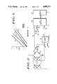
- FIG. 1 is a plot of sensor output voltage versus temperature, and illustrates the kinds of errors which can affect a sensor's output voltage
- FIG. 2 shows a preferred embodiment of a self-calibrating system for processing the outputs of a plurality of sensors according to the invention
- FIG. 3 shows equations which are useful in describing some of the errors which are corrected by the present system and how those errors are preferably compensated for;
- FIGS. 4 and 5 are flow charts illustrating a software program which controls the microprocessor shown in FIG. 2;
- FIG. 6 is a graph depicting the theoretical worst case errors versus sensor temperature for the system shown in FIG. 2, but without utilization of the error correction scheme.
- FIG. 7 is a graph depicting the theoretical worst cases errors versus sensor temperature for the system shown in FIG. 2 for the case in which the present error correction scheme is utilized.
- FIG. 8 shows the theoretical worst case errors between channels for the system shown in FIG. 2 for the case in which the present error correction scheme is utilized.
- a temperature sensor which includes resistors R1 and R T , along with processing circuitry for amplifying the output of the sensor, and correcting circuitry for measuring errors present in the processing circuit and for compensating for the measured errors so as to develop a corrected sensor output signal.
- the ability of the illustrated system to measure and compensate for such errors is due in part to the structure of the illustrated system and in part to a software program to be described later.
- the resistor R1 is preferably a metal film resistor having a one percent tolerance and a temperature coefficient of 50 ppm (parts per million).
- the resistor R T has a resistance which varies with temperature.
- the value of the resistor RT may be approximately 1580 ohms at a temperature of -40° centigrade, and about 3100 ohms at a temperature of +150° centigrade.
- the resistors R1 and R T are coupled as shown in series between a DC supply voltage +V and ground to develop at their junction (node 18) a sensor output signal V T that varies as a function of temperature. It is this signal V T which is to be amplified, processed and corrected as described later herein to provide a sensor signal with high resolution and high accuracy.
- the illustrated system is designed to accommodate a plurality of sensors, as illustrated by the inclusion of resistors 20 and 22 which are connected in series with each other and in parallel with resistors R1 and R T .
- the resistor 20 may be similar to or identical to the resistor R1 and the resistor 22 may be similar to or identical to the resistor R T so as to develop an additional sensor output signal V T1 at the juncture of resistors 20 and 22 (node 24).
- the remainder of the circuitry shown in FIG. 2 essentially comprises circuitry to amplify the output of a selected sensor and to compensate for any errors which are introduced.
- a voltage divider made up of resistors R2 and R3 which are connected in series with each other to develop a reference voltage (V OF ) at their juncture (node 26).
- the resistors R2 and R3 may be of the same type as the resistor R1 described earlier.
- the reference voltage developed at the node 26 is a voltage against which the sensor voltage V T (and other sensor voltages V T1 , etc.) will be compared to develop an amplified sensor output signal.
- an amplifier 28 is included which has a first input terminal 30 coupled to receive the reference signal V OF .
- a second input terminal 32 is coupled to the output of a switch which preferably takes the form of a multiplexer 34 which has multiple inputs.
- the amplifier 28 includes an output terminal 36 at which an amplified signal V O (N) is developed.
- the multiplexer 34 its multiple inputs are shown as including a first input designated as H and additional inputs which are designated as A through G.
- Each of the inputs A-G receives a different sensor output signal.
- the input designated H is selected and used for calibration purposes when the processing circuit is in a calibration mode.
- a selected one of the inputs A-G is amplified and corrected under the control of a programmed microprocessor 40. More specifically, the microprocessor 40 is programmed to enable the multiplexer 34 via an address bus 42 so as to cause the multiplexer 34 to couple its channel H input to the output terminal 38 when the processing circuit is in a calibration mode during which errors in the processing circuit are detected.
- the processing circuit is in the operational mode, a selected one of the other channel inputs A-G becomes coupled to the output terminal 38, and the selected channel input becomes amplified by amplifier 28 and further processed to compensate for any errors detected during the calibration mode.
- the protective impedance network between the output of each sensor and the input to the multiplexer 34 is shown as a resistor 44.
- a resistor 46 is coupled the channel A input to the multiplexer 34 and the node 18.
- another resistor 4 is coupled between the node 26 and the input 30 to the amplifier 28.
- the resistors 44, 46 and 48 are of substantially equal values.
- A/D converter 50 which accepts the analog input from node 36, converts it to a digital value, and inputs it to the microprocessor 40 in the conventional manner.
- A/D converter 50 is illustrated as being a separate item from the microprocessor 40, the A/D converter 50 may be included in the microprocessor 40.
- V T (N) There are two further inputs to the converter 50.
- One is the reference voltage V OF which is coupled to an input of the converter 50 via a line 52.
- the other input to the converter 50 is the signal which appears on the output terminal 38 of the multiplexer 34.
- This input is coupled to the converter 50 via a lead 54 and the voltage thereon is referred to herein as V T (N).
- the voltage V T (N) will correspond to the signal on the one input H or A-G which is selected by the microprocessor to be coupled through the multiplexer 34.
- Amifier offset error is an error which is created by the offset voltage associated with the amplifier 28, and this error is also corrected as described later.
- Bias current error arising from bias currents from the input pins of the amplifier 28 is another form of error which is corrected as described later.
- Another error which is corrected is that due to leakage current through the multiplexer 34.
- This leakage has two distinct components. One such leakage occurs between each input pin of the multiplexer and ground and may be approximately 1 microampere. The other component is due to leakage between input pins and is also in the range of about 1 microampere. Finally, the gain error associated with amplifier 28 is another error which is corrected by the present system.
- FIG. 3 depicts equations 1-4 which are mathematical expressions useful in describing some of the errors discussed above and in describing the type of correction which takes place as described later.
- V O (N) Corrected indicates a sensor output voltage which has been amplified at terminal 36, measured, and compensated for by multiplying the measured voltage at terminal 36 by a factor A and combining the result with a correction factor B.
- a and B are corrective factors which are calculated by the microprocessor 40 in response to measurements made during a calibration cycle. Once the calibration cycle is completed, a sensor output voltage is present on the terminal 36, is measured, and is then corrected by use of the factors A and B as illustrated by equation 1.
- the corrective factor A is defined by equation 2 in which GVI is the ideal voltage gain of the amplifier 28 and dK2 is the gain error as defined by equation 3.
- V O (X) indicates any voltage appearing at the node 36 other than a voltage due to channel H being coupled through the multiplexer to its output terminal 38.
- V O (X) is any amplified sensor output voltage.
- C OFF is a measure of the amplifier offset error plus leakage effects. The calculation of the C OFF is described later.
- V T (X) is a voltage which appears on the lead 54 at the same time that the voltage V O (X) appears on the lead 36.
- V OF is the reference voltage shown at the node 26 in FIG. 2
- V OFI is the ideal reference voltage which would be developed by resistors R2 and R3 in the case where the ratio of R 2 and R 3 has its ideal value.
- the additive corrective factor B is defined by equation 4 where dK3 is the error in the ratio of the resistances of R2 and R3.
- dK3 is the error in the ratio of the resistances of R2 and R3.
- the other factors in equation 4 have already been defined.
- V T (X) and V O (X) are variables which are sensed by the A/D converter 50, digitized, and input to the microprocessor 40 for use in calculating the corrective factors A and B.
- the flow chart shown in FIG. 4 illustrates a software program which is stored in the microprocessor 40.
- This particular program constitutes a calibrate routine by which the A/D converter 50 senses and digitizes selective signals developed by the processing circuit and transfers the digitized information to the microprocessor 40.
- the microprocessor 40 uses the information received from the converter 50 to calculate the corrective factors A and B (see equations 2 and 4).
- the system then goes into its operational mode to initiate a correction routine during which the output of a selective sensor is amplified, the amplified signal is sensed and digitized by the converter 50, and the microprocessor 40 combines the corrective factors A and B with the measured output of the amplifier 28 to provide a corrected output signal as shown by equation 1.
- That output signal may be stored in the microprocessor's memory for further use or may be coupled to an output port (not shown) for transmission to other circuitry as required.
- the calibrate routine begins with an instruction 54 which causes the multiplexer 34 to connect its channel H input terminal to its output terminal 38. This is accomplished by the microprocessor 40 sending the appropriate address to the multiplexer 34 via the bus 42. As a consequence of this action, the input lead 32 of the amplifier 28 receives the channel H signal which comprises the reference voltage V OF plus any voltage drops across the resistor 48 due to leakage currents. The same signal is applied to the other input terminal 30 of the amplifier 28. In addition, the same signal is applied as an input to the converter 50 via the lead 54. The other two inputs to the converter 50 are the amplified output of the amplifier 28 and the reference voltage which is coupled to the converter via the lead 52.
- the next step of the calibration routine causes the microprocessor to store the digitized values of the signals V OF , V O (H), and V T (H) [V O (H) is the value of V O (N) when channel H is selected and V T (H) is the value of V T (N) when the channel H is selected].
- instruction 58 causes the microprocessor to filter the signals V OF and V O (H) to reduce system noise and quantizing error. Such filtering is preferably accomplished by the conventional technique of taking a rolling average which uses a time constant much lager than the sample time of V OF and V O (H).
- instruction 60 causes the microprocessor to calculate dK3 which is the error in the ratio of the resistances of R2 and R3.
- the microprocessor computes the value of this error by subtracting from V OF (the reference voltage) the stored value of the ideal reference voltage V OFI which would be developed in the case where R2 and R3 would have their ideal values.
- the calculated value of dK3 is used later to compute the value of the corrective factor B.
- the next instruction 62 causes the microprocessor to calculate the value of C OFF which is a measure of the offset of the amplifier 28 times its gain plus leakage effects.
- the value of C OFF is calculated by subtracting the filtered value of V OF (measured per instruction 56 and filtered per instruction 58) from the filtered value of V O (H) (also measured per instruction 56 and filtered per instruction 58).
- the calculated value of C OFF will be used later to compute the gain error of the amplifier 28 and also to compute the value of the corrective factors A and B.
- Instruction 64 now causes the microprocessor to select any other sensor channel A-G.
- the channel which is selected is identified as (x).
- This causes the multiplexer 34 to couple one of the channel inputs A-G to its output terminal 38 so that the output of the amplifier 36, now identified V O (X), is an amplified sensor signal as opposed to an output resulting from the calibration mode of operation.
- the next instruction 66 causes the microprocessor to measure the values of V O (X) (the signal now at mode 36) and V T (X) (the signal now on lead 54). The measured values are then filtered (as by the rolling average method mentioned above) per instruction 68.
- the microprocessor has sufficient information, either measured in accordance with the previous instructions or stored in its memory, to calculate the value of dK2 which is the value of the gain error associated with the amplifier 28.
- Instruction 70 causes this calculation to occur as expressed by equation 3 of FIG. 3.
- the microprocessor 40 calculates the value of the multiplier corrective factor A in accordance with equation 2 of FIG. 3.
- instruction 74 causes the microprocessor to calculate the value of the additive corrective factor B as set forth in equation 4.
- dK2 the gain error
- dK3 the error in the offset voltage V OF resulting from the tolerances in R2 and R3.
- the additive factor B will compensate for errors due to the cross products of gain error and offset error.
- the next instruction 56 causes the microprocessor to save the calculated values for A and for B so that they may be used in the correction routine which will now be described.
- the illustrated flow chart depicts the steps used by the microprocessor to correct the measured value of an amplified sensor output signal on one of the channels A-G so as to compensate for the above mentioned errors in the processing circuit.
- instruction 78 causes the microprocessor to enable the multiplexer 34 to select a channel N which will be one of the channels A-G requiring measurement.
- instruction 80 causes the microprocessor to measure the signal at the output of amplifier 28. The measured value of that signal is then multiplied times the corrective factor A which was calculated by the calibrate routine shown in FIG. 4. The result of that multiplication is then, per instruction 84, added to the corrective factor B which was also calculated during the calibrate routine.
- the execution of instructions 82 and 84 have corrected the measured value of the output of amplitude 28 in accordance with equation 1 (FIG. 3). The corrected result is then saved by the microprocessor as required by the next instruction 86.
- the system as thus far described has gone once through its calibrate routine and once through its correction routine. Next, the system may execute its calibrate routine again or it may select a different sensor output signal to process.
- the frequency with which the calibrate routine is used will depend on the environment and other factors associated with a particular application. Suffice it to say that the microprocessor 40 may be programmed to execute the calibrate routine only so often as it is desired to update the information needed to calculate the corrective factors A and B.
- FIGS. 6, 7, and 8 the theoretically worst case errors are shown for the case in which the error correction scheme is not utilized (i.e., the correction routine is disabled). Note that the total error varies from about 7.5 degrees to about 13 degrees as the temperature of the sensor varies between -40° C. and +150° C. This excludes errors in the sensor itself.
- FIG. 7 depicts the theoretically worst case errors for the case in which the correction routine is used, one can see that the errors have been substantially reduced. Over the temperature range of -40° C. to +150° C., the errors vary only between about 1.9 degrees and 2.3 degrees.
- the tracking errors between channels have also been substantially reduced as indicated by FIG. 8. Over the temperature range of -40° C. to +150° C., the theoretically worst case errors vary from about 1.5 degrees to about 1.8 degrees.
- High resolution is achieved by virtue of having an amplified sensor output signal, and high accuracy is achieved because the errors commonly encountered with the amplifier and its associated circuitry are automatically compensated for.
- the system is capable of amplifying and processing a number of different sensor channels such that the channels track with each other because each channel is subject to the same amplification and error correction.
Abstract
Description
Claims (9)
Priority Applications (1)
| Application Number | Priority Date | Filing Date | Title |
|---|---|---|---|
| US06/891,938 US4800513A (en) | 1986-08-01 | 1986-08-01 | Auto-calibrated sensor system |
Applications Claiming Priority (1)
| Application Number | Priority Date | Filing Date | Title |
|---|---|---|---|
| US06/891,938 US4800513A (en) | 1986-08-01 | 1986-08-01 | Auto-calibrated sensor system |
Publications (1)
| Publication Number | Publication Date |
|---|---|
| US4800513A true US4800513A (en) | 1989-01-24 |
Family
ID=25399086
Family Applications (1)
| Application Number | Title | Priority Date | Filing Date |
|---|---|---|---|
| US06/891,938 Expired - Lifetime US4800513A (en) | 1986-08-01 | 1986-08-01 | Auto-calibrated sensor system |
Country Status (1)
| Country | Link |
|---|---|
| US (1) | US4800513A (en) |
Cited By (31)
| Publication number | Priority date | Publication date | Assignee | Title |
|---|---|---|---|---|
| US4875674A (en) * | 1987-02-12 | 1989-10-24 | Concept Ii, Inc. | Energy absorbing means with self calibrating monitor |
| US4912660A (en) * | 1986-12-15 | 1990-03-27 | Ulrich Kuipers | Method and apparatus for measurements of a characteristic of an object using a sensed signal and an auxiliary variable signal applied to the object |
| US4926364A (en) * | 1988-07-25 | 1990-05-15 | Westinghouse Electric Corp. | Method and apparatus for determining weighted average of process variable |
| US4961163A (en) * | 1988-12-02 | 1990-10-02 | Bryan Avron I | System for monitoring and reporting the operability and calibration status of a pH sensor |
| US5016201A (en) * | 1989-02-06 | 1991-05-14 | Bryan Avron I | System for calibrating, monitoring and reporting the status of a pH sensor |
| US5046028A (en) * | 1989-02-06 | 1991-09-03 | Bryan Avron I | System for calibrating, monitoring and reporting the status of a pH sensor |
| US5251157A (en) * | 1990-12-28 | 1993-10-05 | Westinghouse Electric Corp. | Process for offset adjustment of a microprocessor based overcurrent protective device and apparatus |
| US5311452A (en) * | 1990-11-28 | 1994-05-10 | Tokyo Electron Limited | Plasma processing apparatus using capacitance manometer and pressure control method thereof |
| EP0604387A1 (en) * | 1992-12-15 | 1994-06-29 | SBM SCHOELLER-BLECKMANN Medizintechnik Gesellschaft m.b.H. | Measuring arrangement |
| US5343755A (en) * | 1993-05-05 | 1994-09-06 | Rosemount Inc. | Strain gage sensor with integral temperature signal |
| US5347476A (en) * | 1992-11-25 | 1994-09-13 | Mcbean Sr Ronald V | Instrumentation system with multiple sensor modules |
| US5440935A (en) * | 1993-03-18 | 1995-08-15 | Mts Systems Corporation | Apparatus for combining transducer output signals |
| EP0670481A1 (en) * | 1994-01-05 | 1995-09-06 | Becton, Dickinson and Company | Continuously calibrating temperature controller |
| WO1996007872A1 (en) * | 1994-09-10 | 1996-03-14 | Robert Bosch Gmbh | Electronic device |
| US5537340A (en) * | 1992-08-20 | 1996-07-16 | Chrysler Corporation | Method for cancellation of error between digital electronics and a non-ratiometric sensor |
| US5978743A (en) * | 1997-05-30 | 1999-11-02 | Mitutoyo Corporation | Self-calibration method for a sensor |
| US6084394A (en) * | 1995-12-05 | 2000-07-04 | Siemens Aktiengesellschaft | Electronic measuring device using a correction factor to compensate for measuring errors |
| US6249753B1 (en) * | 1998-12-29 | 2001-06-19 | Square D Company | Sensor signal conditioner with calibration |
| US6374191B1 (en) * | 1998-04-20 | 2002-04-16 | Nagano Keiki Co., Ltd. | Self-calibrating sensor |
| US6389371B1 (en) * | 1998-04-14 | 2002-05-14 | Nagano Keiki Co., Ltd. | Signal processing circuit of sensor |
| US6561955B1 (en) | 1999-06-10 | 2003-05-13 | Concept Ii, Inc. | Machine-assisted exercising |
| US20040170213A1 (en) * | 2003-02-27 | 2004-09-02 | Richard Rund | Food safety thermometer |
| US6801868B1 (en) | 2002-10-15 | 2004-10-05 | The United States Of America As Represented By The Administrator Of The National Aeronautics And Space Administration | Real time calibration method for signal conditioning amplifiers |
| US20090071264A1 (en) * | 2007-07-26 | 2009-03-19 | Abb Limited | Flowmeter |
| DE102007052440A1 (en) * | 2007-11-02 | 2009-05-14 | Hottinger Baldwin Messtechnik Gmbh | Method and arrangement of a measuring amplifier for correcting input signals |
| US20110057707A1 (en) * | 2009-09-04 | 2011-03-10 | Rosemount Inc. | Detection and compensation of multiplexer leakage current |
| US20110082015A1 (en) * | 2009-10-02 | 2011-04-07 | Concept Ii, Inc. | Exercising |
| US20150135798A1 (en) * | 2012-05-02 | 2015-05-21 | Robert Bosch Gmbh | Method for ascertaining an offset of an output signal of an evaluation circuit integrated in a sensor, preferably of a pressure sensor installed in a combustion chamber of an internal combustion engine, and sensor |
| WO2018112452A1 (en) | 2016-12-16 | 2018-06-21 | Abb Schweiz Ag | Compensation for ground return differences |
| CN109682500A (en) * | 2018-12-29 | 2019-04-26 | 泰安磐然测控科技有限公司 | A kind of calibrating of temperature measurement device scanning switch and verification system and method |
| CN112997057A (en) * | 2018-09-26 | 2021-06-18 | 德克萨斯仪器股份有限公司 | Method and sensor system with integrated calibration mechanism |
Citations (2)
| Publication number | Priority date | Publication date | Assignee | Title |
|---|---|---|---|---|
| US4280196A (en) * | 1979-11-14 | 1981-07-21 | Hewlett-Packard Company | Correction of zero drift, gain drift, and distortion errors in analog storage devices |
| US4446715A (en) * | 1982-06-07 | 1984-05-08 | Camino Laboratories, Inc. | Transducer calibration system |
-
1986
- 1986-08-01 US US06/891,938 patent/US4800513A/en not_active Expired - Lifetime
Patent Citations (3)
| Publication number | Priority date | Publication date | Assignee | Title |
|---|---|---|---|---|
| US4280196A (en) * | 1979-11-14 | 1981-07-21 | Hewlett-Packard Company | Correction of zero drift, gain drift, and distortion errors in analog storage devices |
| US4446715A (en) * | 1982-06-07 | 1984-05-08 | Camino Laboratories, Inc. | Transducer calibration system |
| US4446715B1 (en) * | 1982-06-07 | 1991-09-17 | Camino Lab Inc |
Cited By (47)
| Publication number | Priority date | Publication date | Assignee | Title |
|---|---|---|---|---|
| US4912660A (en) * | 1986-12-15 | 1990-03-27 | Ulrich Kuipers | Method and apparatus for measurements of a characteristic of an object using a sensed signal and an auxiliary variable signal applied to the object |
| US4875674A (en) * | 1987-02-12 | 1989-10-24 | Concept Ii, Inc. | Energy absorbing means with self calibrating monitor |
| US4926364A (en) * | 1988-07-25 | 1990-05-15 | Westinghouse Electric Corp. | Method and apparatus for determining weighted average of process variable |
| US4961163A (en) * | 1988-12-02 | 1990-10-02 | Bryan Avron I | System for monitoring and reporting the operability and calibration status of a pH sensor |
| US5016201A (en) * | 1989-02-06 | 1991-05-14 | Bryan Avron I | System for calibrating, monitoring and reporting the status of a pH sensor |
| US5046028A (en) * | 1989-02-06 | 1991-09-03 | Bryan Avron I | System for calibrating, monitoring and reporting the status of a pH sensor |
| US5311452A (en) * | 1990-11-28 | 1994-05-10 | Tokyo Electron Limited | Plasma processing apparatus using capacitance manometer and pressure control method thereof |
| US5251157A (en) * | 1990-12-28 | 1993-10-05 | Westinghouse Electric Corp. | Process for offset adjustment of a microprocessor based overcurrent protective device and apparatus |
| US5537340A (en) * | 1992-08-20 | 1996-07-16 | Chrysler Corporation | Method for cancellation of error between digital electronics and a non-ratiometric sensor |
| US5375073A (en) * | 1992-11-25 | 1994-12-20 | Mcbean; Ronald V. | Instrumentation system with multiple sensor modules providing accuracy code information |
| US5347476A (en) * | 1992-11-25 | 1994-09-13 | Mcbean Sr Ronald V | Instrumentation system with multiple sensor modules |
| US5365462A (en) * | 1992-11-25 | 1994-11-15 | Mcbean Sr Ronald V | Instrumentation system with multiple sensor modules providing calibration date information |
| US5377128A (en) * | 1992-11-25 | 1994-12-27 | Mcbean; Ronald V. | Self-calibrating instrumentation system with multiple sensor modules |
| EP0604387A1 (en) * | 1992-12-15 | 1994-06-29 | SBM SCHOELLER-BLECKMANN Medizintechnik Gesellschaft m.b.H. | Measuring arrangement |
| US5426428A (en) * | 1992-12-15 | 1995-06-20 | Sbm Schoeller-Bleckmann Medizintechnik Gesellschaft M.B.H. | Measuring arrangement |
| US5440935A (en) * | 1993-03-18 | 1995-08-15 | Mts Systems Corporation | Apparatus for combining transducer output signals |
| US5343755A (en) * | 1993-05-05 | 1994-09-06 | Rosemount Inc. | Strain gage sensor with integral temperature signal |
| US5519644A (en) * | 1994-01-05 | 1996-05-21 | Becton Dickinson And Company | Continuously calibrating temperature controller |
| EP0670481A1 (en) * | 1994-01-05 | 1995-09-06 | Becton, Dickinson and Company | Continuously calibrating temperature controller |
| WO1996007872A1 (en) * | 1994-09-10 | 1996-03-14 | Robert Bosch Gmbh | Electronic device |
| US6084394A (en) * | 1995-12-05 | 2000-07-04 | Siemens Aktiengesellschaft | Electronic measuring device using a correction factor to compensate for measuring errors |
| US5978743A (en) * | 1997-05-30 | 1999-11-02 | Mitutoyo Corporation | Self-calibration method for a sensor |
| US6389371B1 (en) * | 1998-04-14 | 2002-05-14 | Nagano Keiki Co., Ltd. | Signal processing circuit of sensor |
| US6374191B1 (en) * | 1998-04-20 | 2002-04-16 | Nagano Keiki Co., Ltd. | Self-calibrating sensor |
| US6249753B1 (en) * | 1998-12-29 | 2001-06-19 | Square D Company | Sensor signal conditioner with calibration |
| US7201708B2 (en) | 1999-06-10 | 2007-04-10 | Concept Ii, Inc. | Machine-assisted exercising |
| US6561955B1 (en) | 1999-06-10 | 2003-05-13 | Concept Ii, Inc. | Machine-assisted exercising |
| US6801868B1 (en) | 2002-10-15 | 2004-10-05 | The United States Of America As Represented By The Administrator Of The National Aeronautics And Space Administration | Real time calibration method for signal conditioning amplifiers |
| US20040170213A1 (en) * | 2003-02-27 | 2004-09-02 | Richard Rund | Food safety thermometer |
| US6854883B2 (en) * | 2003-02-27 | 2005-02-15 | F.O.B. Instruments, Ltd. | Food safety thermometer |
| US20090071264A1 (en) * | 2007-07-26 | 2009-03-19 | Abb Limited | Flowmeter |
| US7877220B2 (en) | 2007-07-26 | 2011-01-25 | Abb Limited | Flowmeter |
| DE102007052440A1 (en) * | 2007-11-02 | 2009-05-14 | Hottinger Baldwin Messtechnik Gmbh | Method and arrangement of a measuring amplifier for correcting input signals |
| DE102007052440B4 (en) * | 2007-11-02 | 2009-11-19 | Hottinger Baldwin Messtechnik Gmbh | Method and arrangement of a measuring amplifier for correcting input signals |
| US9069029B2 (en) | 2009-09-04 | 2015-06-30 | Rosemount Inc. | Detection and compensation of multiplexer leakage current |
| US20110057707A1 (en) * | 2009-09-04 | 2011-03-10 | Rosemount Inc. | Detection and compensation of multiplexer leakage current |
| US8098696B2 (en) | 2009-09-04 | 2012-01-17 | Rosemount Inc. | Detection and compensation of multiplexer leakage current |
| US20110082015A1 (en) * | 2009-10-02 | 2011-04-07 | Concept Ii, Inc. | Exercising |
| US20150135798A1 (en) * | 2012-05-02 | 2015-05-21 | Robert Bosch Gmbh | Method for ascertaining an offset of an output signal of an evaluation circuit integrated in a sensor, preferably of a pressure sensor installed in a combustion chamber of an internal combustion engine, and sensor |
| US9518888B2 (en) * | 2012-05-02 | 2016-12-13 | Robert Bosch Gmbh | Method for ascertaining an offset of an output signal of an evaluation circuit integrated in a sensor, preferably of a pressure sensor installed in a combustion chamber of an internal combustion engine, and sensor |
| WO2018112452A1 (en) | 2016-12-16 | 2018-06-21 | Abb Schweiz Ag | Compensation for ground return differences |
| CN110383088A (en) * | 2016-12-16 | 2019-10-25 | Abb瑞士股份有限公司 | The compensation of difference is returned to ground connection |
| EP3555646A4 (en) * | 2016-12-16 | 2021-01-13 | ABB Schweiz AG | Compensation for ground return differences |
| CN112997057A (en) * | 2018-09-26 | 2021-06-18 | 德克萨斯仪器股份有限公司 | Method and sensor system with integrated calibration mechanism |
| CN112997057B (en) * | 2018-09-26 | 2023-07-18 | 德克萨斯仪器股份有限公司 | Method and sensor system with integrated calibration mechanism |
| CN109682500A (en) * | 2018-12-29 | 2019-04-26 | 泰安磐然测控科技有限公司 | A kind of calibrating of temperature measurement device scanning switch and verification system and method |
| CN109682500B (en) * | 2018-12-29 | 2023-11-14 | 山东磐然仪器集团有限公司 | Scanning switch for calibrating temperature metering device and calibrating system and method |
Similar Documents
| Publication | Publication Date | Title |
|---|---|---|
| US4800513A (en) | Auto-calibrated sensor system | |
| US4798093A (en) | Apparatus for sensor compensation | |
| KR100314438B1 (en) | Temperature Measurement Circuit Using Thermopile Sensor | |
| US5469071A (en) | Resistor sensor input apparatus | |
| US4847794A (en) | Error compensation method for transducers having non-linear characteristics, and an assembly for carrying out said method | |
| US20020082799A1 (en) | Measuring transducer with a corrected output signal | |
| US5193393A (en) | Pressure sensor circuit | |
| CA2259378A1 (en) | A system and method for high accuracy calibration of a sensor for offset and sensitivity variation with temperature | |
| CA2145698C (en) | Electronic circuit for a transducer | |
| EP3430414B1 (en) | Crosstalk calibration for multi-channel systems | |
| US4463274A (en) | Temperature compensation circuit for pressure sensor | |
| EP0392746A2 (en) | Transducer temperature compensation circuit | |
| JPS6142876B2 (en) | ||
| US4150433A (en) | Automatic common mode rejection in an analog measuring system | |
| US4556330A (en) | Resistance thermometer and linearization circuitry | |
| US5120954A (en) | Circuit for adjusting encoder signals | |
| US4836027A (en) | Circuit for a sensor | |
| GB1600530A (en) | Two wire current transmitter with adjustable current control linearization | |
| EP4253928A1 (en) | Method for thermoelectric effect error correction | |
| EP1414157B1 (en) | System and method for extending the dynamic range of an analog-to-digital converter | |
| US8872530B2 (en) | Method for correcting the voltage measured across the terminals of a sensor | |
| US6175254B1 (en) | System for compensating a signal for an offset from a reference level | |
| JPH11118617A (en) | Temperature controller | |
| US6535053B2 (en) | Method for obtaining a temperature—independent voltage reference as well as a circuit arrangement for obtaining such a voltage reference | |
| JPH0238920A (en) | Temperature compensated type amplifying circuit |
Legal Events
| Date | Code | Title | Description |
|---|---|---|---|
| AS | Assignment |
Owner name: MOTOROLA, INC., SCHAUMBURG, ILLINOIS, A CORP. OF D Free format text: ASSIGNMENT OF ASSIGNORS INTEREST.;ASSIGNOR:DEUTSCH, ROBERT W.;REEL/FRAME:004586/0797 Effective date: 19860729 Owner name: MOTOROLA, INC.,ILLINOIS Free format text: ASSIGNMENT OF ASSIGNORS INTEREST;ASSIGNOR:DEUTSCH, ROBERT W.;REEL/FRAME:004586/0797 Effective date: 19860729 |
|
| STCF | Information on status: patent grant |
Free format text: PATENTED CASE |
|
| CC | Certificate of correction | ||
| FPAY | Fee payment |
Year of fee payment: 4 |
|
| FPAY | Fee payment |
Year of fee payment: 8 |
|
| FPAY | Fee payment |
Year of fee payment: 12 |
|
| AS | Assignment |
Owner name: TEMIC AUTOMOTIVE OF NORTH AMERICA, INC., ILLINOIS Free format text: ASSIGNMENT OF ASSIGNORS INTEREST;ASSIGNOR:MOTOROLA, INC.;REEL/FRAME:018471/0170 Effective date: 20061016 |