US4755820A - Antenna device - Google Patents
Antenna device Download PDFInfo
- Publication number
- US4755820A US4755820A US06/892,427 US89242786A US4755820A US 4755820 A US4755820 A US 4755820A US 89242786 A US89242786 A US 89242786A US 4755820 A US4755820 A US 4755820A
- Authority
- US
- United States
- Prior art keywords
- antenna
- patch
- antenna device
- dielectric
- coupling member
- Prior art date
- Legal status (The legal status is an assumption and is not a legal conclusion. Google has not performed a legal analysis and makes no representation as to the accuracy of the status listed.)
- Expired - Fee Related
Links
Images


Classifications
-
- H—ELECTRICITY
- H01—ELECTRIC ELEMENTS
- H01Q—ANTENNAS, i.e. RADIO AERIALS
- H01Q9/00—Electrically-short antennas having dimensions not more than twice the operating wavelength and consisting of conductive active radiating elements
- H01Q9/04—Resonant antennas
- H01Q9/0407—Substantially flat resonant element parallel to ground plane, e.g. patch antenna
-
- H—ELECTRICITY
- H01—ELECTRIC ELEMENTS
- H01Q—ANTENNAS, i.e. RADIO AERIALS
- H01Q19/00—Combinations of primary active antenna elements and units with secondary devices, e.g. with quasi-optical devices, for giving the antenna a desired directional characteristic
- H01Q19/06—Combinations of primary active antenna elements and units with secondary devices, e.g. with quasi-optical devices, for giving the antenna a desired directional characteristic using refracting or diffracting devices, e.g. lens
- H01Q19/062—Combinations of primary active antenna elements and units with secondary devices, e.g. with quasi-optical devices, for giving the antenna a desired directional characteristic using refracting or diffracting devices, e.g. lens for focusing
-
- H—ELECTRICITY
- H01—ELECTRIC ELEMENTS
- H01Q—ANTENNAS, i.e. RADIO AERIALS
- H01Q19/00—Combinations of primary active antenna elements and units with secondary devices, e.g. with quasi-optical devices, for giving the antenna a desired directional characteristic
- H01Q19/10—Combinations of primary active antenna elements and units with secondary devices, e.g. with quasi-optical devices, for giving the antenna a desired directional characteristic using reflecting surfaces
- H01Q19/12—Combinations of primary active antenna elements and units with secondary devices, e.g. with quasi-optical devices, for giving the antenna a desired directional characteristic using reflecting surfaces wherein the surfaces are concave
- H01Q19/13—Combinations of primary active antenna elements and units with secondary devices, e.g. with quasi-optical devices, for giving the antenna a desired directional characteristic using reflecting surfaces wherein the surfaces are concave the primary radiating source being a single radiating element, e.g. a dipole, a slot, a waveguide termination
Definitions
- This invention relates to an antenna device of the kind used to radiate the output of an electromagnetic power source into free space.
- Antenna devices are known. These include wire antennae and waveguide horns. An antenna is driven by a power source via an impedance matching network.
- the network is required because typical solid state power sources such as Gunn or impatt diodes have impedances much lower than that of a wire antenna or waveguide horn.
- the matching network is not incorporated monolithically in the solid state power source structure since this is not necessarily technically feasible and is wasteful of valuable semiconductor material in any event Antenna devices are accordingly usually of hybrid form.
- the reactance of the power source is then a function of bond wire connections and the like. The result is that solid state power sources require individual manual adjustment. At higher frequencies in particular, matching requires the use of waveguide cavities which are heavy and bulky relative to the power source or antenna. Moreover, the required degree of mismatch reduction reduces power amplifier bandwidth.
- microstrip patch antennae have been developed.
- Such an antenna typically consists of a planar rectangular patch of metal on one surface of a dielectric substrate sheet, the other surface bearing a ground plane.
- the antenna impedance can be arranged to allow a power source to be integrated directly into the antenna structure without an intervening matching network.
- radiative efficiency is low and bandwidth severely limited for such an antenna as compared to conventional types. Radiative efficiency is low because much of the energy radiated by a patch antenna of known kind is trapped within the substrate layer, and only a small proportion is radiated into free space. Similar effects have been analysed by Brewitt-Taylor, Gunton and Rees in Electronics Letters, 1st Oct. 1981, Vol 17, pp 729-731.
- the present invention provides an antenna device comprising a conducting antenna patch spaced from a conducting ground plane by the thickness of a dielectric sheet, means for energizing the antenna patch, and a low-loss dielectric coupling member arranged over the antenna patch to couple radiation from it away from the dielectric sheet, and coupling member having a dielectric constant at least twice the dielectric constant of the sheet, and having a cross-sectional area reducing with distance from the antenna patch.
- ground plane is herein employed in accordance with its ordinary signification in the art as meaning a normally but not necessarily flat conducting sheet for earthing purposes.
- the invention provides an antenna device capable of coupling power from a source to free space with higher efficiency than a prior art microstrip patch antenna device.
- radiation trapping in the dielectric sheet is avoided.
- the invention is characterised by design geometry features such as dielectric sheet thickness which can easily be selected to provide impedance matching of the antenna device to a power source. There is therefore no need for a matching network.
- the invention accordingly provides the efficiency of conventional wire antennae, waveguide horns and matching networks combined with the ease of construction of prior art microstrip patch antennae.
- the antennae device is arranged to be at or above quarter wavelength resonance; the means for energising the patch antenna comprises a power source connected to one longitudinal end of the patch.
- the device may have a dielectric coupling member in the form of a lens. This provides an antenna radiation pattern substantially in the form of a relatively narrow cone centred on the antenna boresight, which is particularly advantageous in use.
- the antenna patch may conveniently be a planar and rectangular metal element.
- the said at least one dielectric element may be a plurality of elements, but is conveniently a single sheet of low loss material. It may be plastics material of dielectric constant in the region of 2.5.
- the dielectric coupling member preferably has a dielectric constant of more than twice, and preferably at least three times that of the sheet, and may be of alumina with dielectric constant 9.8.
- the means for energising the antenna patch may be a discrete solid state device arranged between the ground plane and patch and accommodated within the dielectric sheet. Such means may alternatively be a coaxial power connection made through a hole in the ground plane and passing via the dielectric sheet.
- the dielectric sheet may be of high resistivity and hence low loss semiconductor material into which a solid state power source is integrated.
- the semiconductor material may be Si, in which case the coupling member may be barium nona-titanate with a dielectric constant of 36.
- the antenna device may be provided with focussing means to produce a parallel output beam.
- the dielectric coupling member may have a tapering cross-section suitable for launching radiation into a waveguide.
- the antenna device of the invention may be arranged with other like devices to form an array.
- FIG. 1 schematically shows an antenna device of the invention
- FIGS. 2 and 3 are side and plan views of part of the FIG. 1 device illustrating power source provision
- FIG. 4 illustrates a coaxial power connection for the FIG. 1 device
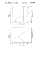
- FIGS. 5 and 6 provide impedance data as a function of frequency for the FIG. 1 device
- FIG. 7 provides measured output radiation patterns for the FIG. 1 device with power fed to one end of the antenna patch
- FIG. 8 illustrates the radiation pattern arising from a coaxial power connection
- FIG. 9 provides theoretical radiation patterns for a device of the invention with power fed to one end of the antenna patch
- FIG. 10 illustrates the measured radiation pattern obtained from a device of the invention when power is fed to the centre of the antenna patch
- FIG. 11 schematically shows an antenna device of the invention appropriate for forming part of an array
- FIGS. 12 and 13 illustrate parallel output beam production from a device of the invention.
- FIG. 14 illustrates use of the invention to launch radiation into a waveguide.
- FIG. 1 there is shown a sectional view of an antenna device of the invention indicated generally by 10.
- the device consists of a planar and rectangular metal conductor or antenna patch 12 arranged horizontally on one surface 14 of a dielectric sheet substrate 16.
- the width dimension of the patch 12 is perpendicular to the plane of the drawing.
- a metal ground plane 18 is disposed on the other surface 20 of the substrate 16.
- the substrate 16 is of proprietary material designated "Plastikard", and manufactured by Slater's Partard Ltd, a British Company. It has low loss and low permittivity.
- the substrate 16 may alternatively be of polytetrafluorethylene (PTFE) of dielectric constant 2.1.
- PTFE polytetrafluorethylene
- a hemispherical dielectric lens 22 having a curved surface 24 is arranged over and in intimate contact with the antenna patch 12.
- the lens 22 is of alumina having a dielectric constant of 9.8.
- a microwave power source indicated generally by 26 is connected between the patch 12 and ground plane 18 through the substrate 16, as will be described later in more detail.
- the antenna device 10 operates as follows. Since the lens 22 is of higher dielectric constant than the substrate 16, radiation from the antenna patch 12 is coupled predominantly into the lens 22 away from the substrate 16. Moreover, the lens 22 has a focussing effect which directs the radiation as a beam into free space beyond the surface 24. The result is that power from the source 26 is radiated into free space with greater efficiency than is possible with a prior art microstrip patch antenna, since power is predominantly coupled away from the substrate 16 to which radiation is lost in the prior art.
- the substrate 16 has a hole 30 to accommodate a discrete solid state power source 26 such as a Gunn diode or an impatt diode.
- the diode power source 26 is provided with DC bias relative to the ground plane -8 via a connection 32 to the antenna patch 12.
- the dielectric sheet substrate 16 may be of low loss semiconductor material such as Si or GaAs into which a solid state power source 26 is integrated.
- a substrate of Si with a dielectric constant of 12 an associated dielectric member or lens 22 of barium nona-titanate may be employed having a dielectric constant of 36.
- FIG. 4 there is illustrated power coupling or current feed to the antenna patch 12 via a coaxial line 40.
- the line 40 extends vertically, ie perpendicular to the plane of the patch 12. It passes through a hole 42 in the ground plane 18 and thence via the dielectric substrate 16 to the patch 12.
- Impedance measurements have been made on the antenna device 10 as a function of drive position or power source connection point along the length of the antenna patch 12. Measurements were made using a coaxial feed as shown in FIG. 4 together with a network analyser. It has been found surprisingly that the condition for resonance is that the effective antenna length from the drive point is one quarter of a wavelength (or multiples thereof) at the interface between the two dielectrics 16 and 22. Moreover, the current in the antenna patch 12 runs outwards, ie away from the drive point in both directions along the patch. This is quite different to the situation in prior art patch antennae, in which current runs undirectionally from one end to the other and resonance occurs at an effective antenna length of one half of a wavelength irrespective of drive position.
- FIGS. 5 and 6 there are shown respectively measurements of conductance and susceptance in milli-siemens (ms) plotted against frequency in GHz for an antenna device of the invention.
- the measurements were made on a device generally similar to that described earlier with reference to FIGS. 1 and 4, except that the hemispherical lens 22 was replaced by an alumina lens having a focal plane in which the antenna patch was located. Radiation passing through the lens was absorbed in water providing a non-reflecting lossy load. This avoids reflection back to the patch.
- the patch itself had a length of 3.5 mm and a width of 1 mm, and was connected at one end to a power source. The thickness h of the dielectric sheet between patch and ground plane was 0.54 mm.
- antenna resonance occurs at about 9.1 GHz.
- Further measurements (not illustrated) on antenna devices of the invention with different values of h indicate that resonant impedance varies linearly with h for h much less than a quarter of a wavelength. Impedance is expected to be a maximum when h is approximately a quarter of a wavelength, the impedance then having a value determined by antenna patch dimensions and the dielectric constants of the two adjacent media.
- the resonant antenna device impedance is only a few ohms.
- the reciprocal of the maximum measured conductance of about 400 ms at 9.1 GHz is 2.5 ohms.
- the resonant impedance can be altered by varying h, antenna dimensions and media dielectric constants. Since typical power source impedances are also of the order of a few ohms, it is straightforward to design antenna devices of the invention for impedance matching to power sources.
- FIG. 7 there are shown graphs 50 and 52 in polar coordinates of power (arbitrary units) radiated by an antenna device of the invention plotted as a function of angle.
- the graphs 50 and 52 relate to the E and H planes respectively, and extend upwardly of the plane of a corresponding horizontal antenna patch such as 12 in FIG. 1.
- the FIG. 7 data were obtained at 8 GHz using an arrangement generally similar to that of FIG. 1 with the vertical current feed shown in FIG. 4. Detail differences are as follows.
- a hemispherical lens similar to 22 was employed, but it was of a commercially available material designated PT9.8 and manufactured by Marcoi Electronic Devices Ltd, a British company.
- the lens curved surface had an antireflection coating.
- the antenna patch was 5 mm in length, and power connection was made at one end. It can be seen that radiation is directed into a comparatively narrow cone for both graphs 50 and 52.
- Graph 50 is asymmetric due to the effect of the antenna patch current feed which also radiates. Detection of this effect in the H-plane is avoided, because H-plane contributions from the current feed and antenna patch are polarised orthogonally to one another and can be detected separately.
- FIG. 8 there is shown a graph of radiated power as a function of angle in polar coordinates for a current feed to an antenna patch.
- the patch was 4 mm long, power connection was made to one end and measurements were made at 7 GHz in the H-plane.
- the H-plane current feed radiation is detectable independently of that from the antenna patch.
- the graph consists of two lobes 60a and 60b arranged substantially symmetrically about the vertical or boresight direction.
- the E-plane equivalent of the right-hand lobe 60b becomes combined with the antenna patch E-plane radiation to produce the asymmetry shown in graph 50 in FIG. 7.
- the E-plane equivalent of the left-hand lobe 60a is much weaker because of the blocking effect of the antenna patch, and does not make a significant contribution to the graph 50.
- FIG. 9 there is shown a theoretical radiation pattern for an antenna device of the invention.
- the pattern is calculated for a device as shown in FIG. 1 operating at 9.8 GHz, and to which power is fed at one end of the antenna patch.
- the device parameters employed were antenna patch length 5 mm, substrate thickness (h) 0.86 mm, and lens and substrate dielectric constants 10 and 2.5 respectively.
- the pattern includes an E-plane graph 70 (solid line) and an H-plane te graph 72 (broken line).
- Graph 74 shows the H-plane tm pattern (chain line).
- the calculated antenna radiation pattern indicates output into a comparatively narrow cone in agreement with the measurements discussed previously. It will be noted that the antenna radiation pattern intensity is zero in the (horizontal) plane of the antenna patch.
- FIG. 10 there is shown a further radiation pattern illustrating the effect of power connection to the centre of an antenna patch of the invention.
- Power measurement was carried out at 8 GHz in the E-plane using an antenna patch 10 mm in length.
- the radiation pattern consists of two narrow lobes 80a and 80b arranged fairly symmetrically about boresight, at which there is a null.
- the null occurs since currents run outwards from the power connection point at the centre of the antenna patch, and the two ends of the patch are radiating in antiphase. This is quite different to conventional microstrip patch antennae, in which currents run along the patch independently of the power connection position.
- FIGS. 11 to 14 inclusive there are schematically illustrated various implementations of antenna devices of the invention each similar to that shown in FIG. 1.
- an antenna device 90 is shown arranged to radiate into free space.
- the device 90 may be used either alone or accompanied by equivalent devices (indicated by chain lines 92) to form an array.
- a device 94 is shown furnished with an additional dielectric lens 96 of concavo-convex form
- the lens 96 has an inner concave surface 98 complementary to and in contact with the lens 100 of the device 94.
- the lenses 98 and 100 form a multiple component lens which produces a parallel output beam from the device 94 as indicated at 102.
- the device output 104 may alternatively be rendered parallel using a mirror 106.
- FIG. 14 shows a sectional view of an antenna device 110 arranged as a launcher to input radiation to a waveguide 112.
- the device 10 has a tapering dielectric coupling member 114 for coupling radiation from the antenna patch to the waveguide.
- This member 114 replaces the hemispherical lens of earlier embodiments.
- the cross-section of the coupling member 114 perpendicular to the plane of the drawing is circular.
- this section is rectangular.
- the invention provides an antenna device characterised by ease of construction and impedance matching to a power source, high efficiency and advantageous output radiation pattern.
- the efficiency of coupling a power source to free space is theoretically 100%.
- a prior art microstrip patch antenna is at best about 70% efficient when a low permittivity dielectric substrate is used for the antenna patch. If a silicon substrate were to be used in order to incorporate within it an integrated power source, the efficiency would fall to around 20%. This is because radiation is trapped in the substrate of the prior art device. This results in power loss to the substrate to a degree varying with substrate dielectric constant.
- the prior art device is unsuitable for use as a member of an array.
- Coupling between adjacent devices would occur, because each radiation pattern does not fall to zero in the plane of the antenna patch, unlike the invention. Moreover, coupling via the substrate would occur in a prior art array on a common substrate. In contrast, the invention radiates away from the plane of the antenna patch into a comparatively narrow cone from which a substantially parallel output beam can easily be produced. In addition, a semiconductor antenna patch substrate may be employed and a power source integrated therein. Since radiation output is zero in the plane of the antenna patch, the invention is ideally suited to producing arrays of antenna devices which do not couple together.
Abstract
Description
Claims (8)
Applications Claiming Priority (2)
| Application Number | Priority Date | Filing Date | Title |
|---|---|---|---|
| GB8519900 | 1985-08-08 | ||
| GB8519900 | 1985-08-08 |
Publications (1)
| Publication Number | Publication Date |
|---|---|
| US4755820A true US4755820A (en) | 1988-07-05 |
Family
ID=10583480
Family Applications (1)
| Application Number | Title | Priority Date | Filing Date |
|---|---|---|---|
| US06/892,427 Expired - Fee Related US4755820A (en) | 1985-08-08 | 1986-08-04 | Antenna device |
Country Status (2)
| Country | Link |
|---|---|
| US (1) | US4755820A (en) |
| EP (1) | EP0217426A3 (en) |
Cited By (43)
| Publication number | Priority date | Publication date | Assignee | Title |
|---|---|---|---|---|
| US4901086A (en) * | 1987-10-02 | 1990-02-13 | Raytheon Company | Lens/polarizer radome |
| US5087920A (en) * | 1987-07-30 | 1992-02-11 | Sony Corporation | Microwave antenna |
| US5239304A (en) * | 1987-01-05 | 1993-08-24 | Harada Kogyo Kabushiki Kaisha | Three-wave antenna for vehicles |
| US5493719A (en) * | 1994-07-01 | 1996-02-20 | The United States Of America As Represented By The Secretary Of The Air Force | Integrated superconductive heterodyne receiver |
| EP0755092A2 (en) * | 1995-07-17 | 1997-01-22 | Plessey Semiconductors Limited | Antenna arrangements |
| US5631659A (en) * | 1995-03-17 | 1997-05-20 | Lucent Technologies Inc. | Microstrip patch antennas with radiation control |
| US5642103A (en) * | 1990-10-01 | 1997-06-24 | Sharp Kabushiki Kaisha | Transponder used in a remote identification system |
| EP0786825A1 (en) * | 1996-01-18 | 1997-07-30 | Murata Manufacturing Co., Ltd. | Dielectric lens apparatus |
| EP0814533A2 (en) * | 1996-06-21 | 1997-12-29 | SIBET Gmbh SICAN FORSCHUNGS- UND ENTWICKLUNGSBETRIEBSGESELLSCHAFT mbH | Directional antenna for radio telephone |
| US5706017A (en) * | 1993-04-21 | 1998-01-06 | California Institute Of Technology | Hybrid antenna including a dielectric lens and planar feed |
| US5764199A (en) * | 1995-08-28 | 1998-06-09 | Datron/Transco, Inc. | Low profile semi-cylindrical lens antenna on a ground plane |
| US5781163A (en) * | 1995-08-28 | 1998-07-14 | Datron/Transco, Inc. | Low profile hemispherical lens antenna array on a ground plane |
| WO1998054788A1 (en) * | 1997-05-30 | 1998-12-03 | Robert Bosch Gmbh | Antenna for high frequency radio signal transmission |
| US5929819A (en) * | 1996-12-17 | 1999-07-27 | Hughes Electronics Corporation | Flat antenna for satellite communication |
| US6005519A (en) * | 1996-09-04 | 1999-12-21 | 3 Com Corporation | Tunable microstrip antenna and method for tuning the same |
| US6011524A (en) * | 1994-05-24 | 2000-01-04 | Trimble Navigation Limited | Integrated antenna system |
| US6046701A (en) * | 1997-11-03 | 2000-04-04 | Spike Technologies, Inc. | Apparatus for high-performance sectored antenna system |
| US6061036A (en) * | 1998-02-03 | 2000-05-09 | Ericsson, Inc. | Rigid and flexible antenna |
| US6075492A (en) * | 1997-02-06 | 2000-06-13 | Robert Bosch Gmbh | Microwave antenna array for a motor vehicle radar system |
| US6169525B1 (en) | 1998-09-10 | 2001-01-02 | Spike Technologies, Inc. | High-performance sectored antenna system using low profile broadband feed devices |
| US6246369B1 (en) * | 1999-09-14 | 2001-06-12 | Navsys Corporation | Miniature phased array antenna system |
| US6518932B1 (en) * | 1999-02-15 | 2003-02-11 | Communications Research Laboratory, Independent Administrative Institute | Radio communication device |
| US6549172B1 (en) * | 1999-11-18 | 2003-04-15 | Centre National De La Recherche Scientifique (C.N.R.S.) | Antenna provided with an assembly of filtering materials |
| US6590544B1 (en) * | 1998-09-01 | 2003-07-08 | Qualcomm, Inc. | Dielectric lens assembly for a feed antenna |
| US6624792B1 (en) | 2002-05-16 | 2003-09-23 | Titan Systems, Corporation | Quad-ridged feed horn with two coplanar probes |
| US6844552B2 (en) | 2000-04-06 | 2005-01-18 | Rensselaer Polytechnic Institute | Terahertz transceivers and methods for emission and detection of terahertz pulses using such transceivers |
| US20050162316A1 (en) * | 2002-05-15 | 2005-07-28 | Rebecca Thomas | Improvements relating to attaching antenna structures to electrical feed structures |
| US20050225499A1 (en) * | 2002-03-26 | 2005-10-13 | Kingsley Simon P | Dielectric resonator antenna |
| US20050242996A1 (en) * | 2002-08-14 | 2005-11-03 | Palmer Tim J | Electrically small dielectric antenna with wide bandwidth |
| US20070229363A1 (en) * | 2006-03-29 | 2007-10-04 | Fujitsu Component Limited | Antenna device |
| US20080180336A1 (en) * | 2007-01-31 | 2008-07-31 | Bauregger Frank N | Lensed antenna methods and systems for navigation or other signals |
| US20100328779A1 (en) * | 2009-06-30 | 2010-12-30 | California Institute Of Technolology | Dielectric covered planar antennas |
| US20120228563A1 (en) * | 2008-08-28 | 2012-09-13 | Alliant Techsystems Inc. | Composites for antennas and other applications |
| US20140144009A1 (en) * | 2012-04-24 | 2014-05-29 | California Institute Of Technology | Microfabrication Technique of Silicon Microlens Array for Terahertz Applications |
| CN104037505A (en) * | 2014-05-27 | 2014-09-10 | 东南大学 | Three-dimensional amplifying lens |
| US20150116154A1 (en) * | 2012-07-10 | 2015-04-30 | Limited Liability Company "Radio Gigabit" | Lens antenna with electronic beam steering capabilities |
| US20150253421A1 (en) * | 2012-10-05 | 2015-09-10 | Hitachi Automotive Systems, Ltd. | Radar Module and Speed Measuring Device Using Same |
| WO2016081515A1 (en) | 2014-11-18 | 2016-05-26 | Commscope Technologies Llc | Antenna having dielectric sheet loading to control beam width |
| USD775331S1 (en) | 2015-03-02 | 2016-12-27 | Covidien Lp | Hand-held antenna system |
| USD806691S1 (en) * | 2015-11-23 | 2018-01-02 | Hms Industrial Networks Ab | Communications equipment |
| US20180191071A1 (en) * | 2017-01-05 | 2018-07-05 | Fraunhofer-Gesellschaft Zur Foerderung Der Angewandten Forschung E.V. | Ndip antenna |
| CN108493581A (en) * | 2018-03-28 | 2018-09-04 | 中国科学院福建物质结构研究所 | A kind of Terahertz antenna structure and the radiation source including the antenna structure and detector |
| US10826196B1 (en) * | 2019-04-11 | 2020-11-03 | The Boeing Company | Dielectric lens antenna |
Families Citing this family (3)
| Publication number | Priority date | Publication date | Assignee | Title |
|---|---|---|---|---|
| AU4657897A (en) * | 1996-09-30 | 1998-04-24 | Qualcomm Incorporated | Dielectric lens assembly for a feed antenna |
| AU2452799A (en) * | 1999-01-07 | 2000-07-24 | Spike Broadband Systems, Inc. | Apparatus for high-performance sectored antenna system |
| CN106796652A (en) | 2014-08-11 | 2017-05-31 | 辛纳普蒂克斯公司 | Multi views fingerprint matching |
Citations (6)
| Publication number | Priority date | Publication date | Assignee | Title |
|---|---|---|---|---|
| US4012741A (en) * | 1975-10-07 | 1977-03-15 | Ball Corporation | Microstrip antenna structure |
| US4072952A (en) * | 1976-10-04 | 1978-02-07 | The United States Of America As Represented By The Secretary Of The Army | Microwave landing system antenna |
| GB2131232A (en) * | 1982-09-27 | 1984-06-13 | Rogers Corp | Microstrip antenna and method of manufacture thereof |
| US4490721A (en) * | 1980-11-17 | 1984-12-25 | Ball Corporation | Monolithic microwave integrated circuit with integral array antenna |
| US4600018A (en) * | 1982-06-02 | 1986-07-15 | National Research Development Corporation | Electromagnetic medical applicators |
| US4654622A (en) * | 1985-09-30 | 1987-03-31 | Honeywell Inc. | Monolithic integrated dual mode IR/mm-wave focal plane sensor |
Family Cites Families (1)
| Publication number | Priority date | Publication date | Assignee | Title |
|---|---|---|---|---|
| EP0117017A1 (en) * | 1983-01-20 | 1984-08-29 | Hazeltine Corporation | Low-profile omni-antenna |
-
1986
- 1986-08-04 EP EP86201363A patent/EP0217426A3/en not_active Withdrawn
- 1986-08-04 US US06/892,427 patent/US4755820A/en not_active Expired - Fee Related
Patent Citations (6)
| Publication number | Priority date | Publication date | Assignee | Title |
|---|---|---|---|---|
| US4012741A (en) * | 1975-10-07 | 1977-03-15 | Ball Corporation | Microstrip antenna structure |
| US4072952A (en) * | 1976-10-04 | 1978-02-07 | The United States Of America As Represented By The Secretary Of The Army | Microwave landing system antenna |
| US4490721A (en) * | 1980-11-17 | 1984-12-25 | Ball Corporation | Monolithic microwave integrated circuit with integral array antenna |
| US4600018A (en) * | 1982-06-02 | 1986-07-15 | National Research Development Corporation | Electromagnetic medical applicators |
| GB2131232A (en) * | 1982-09-27 | 1984-06-13 | Rogers Corp | Microstrip antenna and method of manufacture thereof |
| US4654622A (en) * | 1985-09-30 | 1987-03-31 | Honeywell Inc. | Monolithic integrated dual mode IR/mm-wave focal plane sensor |
Cited By (62)
| Publication number | Priority date | Publication date | Assignee | Title |
|---|---|---|---|---|
| US5239304A (en) * | 1987-01-05 | 1993-08-24 | Harada Kogyo Kabushiki Kaisha | Three-wave antenna for vehicles |
| US5087920A (en) * | 1987-07-30 | 1992-02-11 | Sony Corporation | Microwave antenna |
| US4901086A (en) * | 1987-10-02 | 1990-02-13 | Raytheon Company | Lens/polarizer radome |
| US5642103A (en) * | 1990-10-01 | 1997-06-24 | Sharp Kabushiki Kaisha | Transponder used in a remote identification system |
| US5706017A (en) * | 1993-04-21 | 1998-01-06 | California Institute Of Technology | Hybrid antenna including a dielectric lens and planar feed |
| US6011524A (en) * | 1994-05-24 | 2000-01-04 | Trimble Navigation Limited | Integrated antenna system |
| US5493719A (en) * | 1994-07-01 | 1996-02-20 | The United States Of America As Represented By The Secretary Of The Air Force | Integrated superconductive heterodyne receiver |
| US5631659A (en) * | 1995-03-17 | 1997-05-20 | Lucent Technologies Inc. | Microstrip patch antennas with radiation control |
| EP0755092A2 (en) * | 1995-07-17 | 1997-01-22 | Plessey Semiconductors Limited | Antenna arrangements |
| EP0755092A3 (en) * | 1995-07-17 | 1999-04-14 | Mitel Semiconductor Limited | Antenna arrangements |
| US5757323A (en) * | 1995-07-17 | 1998-05-26 | Plessey Semiconductors Limited | Antenna arrangements |
| US5781163A (en) * | 1995-08-28 | 1998-07-14 | Datron/Transco, Inc. | Low profile hemispherical lens antenna array on a ground plane |
| US5764199A (en) * | 1995-08-28 | 1998-06-09 | Datron/Transco, Inc. | Low profile semi-cylindrical lens antenna on a ground plane |
| EP0786825A1 (en) * | 1996-01-18 | 1997-07-30 | Murata Manufacturing Co., Ltd. | Dielectric lens apparatus |
| US5900847A (en) * | 1996-01-18 | 1999-05-04 | Murata Manufacturing Co., Ltd. | Dielectric lens apparatus |
| EP0814533A2 (en) * | 1996-06-21 | 1997-12-29 | SIBET Gmbh SICAN FORSCHUNGS- UND ENTWICKLUNGSBETRIEBSGESELLSCHAFT mbH | Directional antenna for radio telephone |
| EP0814533A3 (en) * | 1996-06-21 | 2000-05-03 | SIBET Gmbh SICAN FORSCHUNGS- UND ENTWICKLUNGSBETRIEBSGESELLSCHAFT mbH | Directional antenna for radio telephone |
| US6005519A (en) * | 1996-09-04 | 1999-12-21 | 3 Com Corporation | Tunable microstrip antenna and method for tuning the same |
| US5929819A (en) * | 1996-12-17 | 1999-07-27 | Hughes Electronics Corporation | Flat antenna for satellite communication |
| US6075492A (en) * | 1997-02-06 | 2000-06-13 | Robert Bosch Gmbh | Microwave antenna array for a motor vehicle radar system |
| US6310587B1 (en) * | 1997-05-30 | 2001-10-30 | Robert Bosch Gmbh | Antenna for high frequency radio signal transmission |
| WO1998054788A1 (en) * | 1997-05-30 | 1998-12-03 | Robert Bosch Gmbh | Antenna for high frequency radio signal transmission |
| US6046701A (en) * | 1997-11-03 | 2000-04-04 | Spike Technologies, Inc. | Apparatus for high-performance sectored antenna system |
| US6061036A (en) * | 1998-02-03 | 2000-05-09 | Ericsson, Inc. | Rigid and flexible antenna |
| US6590544B1 (en) * | 1998-09-01 | 2003-07-08 | Qualcomm, Inc. | Dielectric lens assembly for a feed antenna |
| US6169525B1 (en) | 1998-09-10 | 2001-01-02 | Spike Technologies, Inc. | High-performance sectored antenna system using low profile broadband feed devices |
| US6518932B1 (en) * | 1999-02-15 | 2003-02-11 | Communications Research Laboratory, Independent Administrative Institute | Radio communication device |
| US6246369B1 (en) * | 1999-09-14 | 2001-06-12 | Navsys Corporation | Miniature phased array antenna system |
| US6549172B1 (en) * | 1999-11-18 | 2003-04-15 | Centre National De La Recherche Scientifique (C.N.R.S.) | Antenna provided with an assembly of filtering materials |
| US6844552B2 (en) | 2000-04-06 | 2005-01-18 | Rensselaer Polytechnic Institute | Terahertz transceivers and methods for emission and detection of terahertz pulses using such transceivers |
| US20050225499A1 (en) * | 2002-03-26 | 2005-10-13 | Kingsley Simon P | Dielectric resonator antenna |
| US7253789B2 (en) * | 2002-03-26 | 2007-08-07 | Antenova Ltd. | Dielectric resonator antenna |
| US20050162316A1 (en) * | 2002-05-15 | 2005-07-28 | Rebecca Thomas | Improvements relating to attaching antenna structures to electrical feed structures |
| US7183975B2 (en) * | 2002-05-15 | 2007-02-27 | Antenova Ltd. | Attaching antenna structures to electrical feed structures |
| US6624792B1 (en) | 2002-05-16 | 2003-09-23 | Titan Systems, Corporation | Quad-ridged feed horn with two coplanar probes |
| US20050242996A1 (en) * | 2002-08-14 | 2005-11-03 | Palmer Tim J | Electrically small dielectric antenna with wide bandwidth |
| US7161535B2 (en) | 2002-08-14 | 2007-01-09 | Antenova Ltd. | Electrically small dielectric antenna with wide bandwidth |
| US20070229363A1 (en) * | 2006-03-29 | 2007-10-04 | Fujitsu Component Limited | Antenna device |
| US7382331B2 (en) * | 2006-03-29 | 2008-06-03 | Fujitsu Component Limited | Antenna device |
| US20080180336A1 (en) * | 2007-01-31 | 2008-07-31 | Bauregger Frank N | Lensed antenna methods and systems for navigation or other signals |
| US20120228563A1 (en) * | 2008-08-28 | 2012-09-13 | Alliant Techsystems Inc. | Composites for antennas and other applications |
| US8723722B2 (en) * | 2008-08-28 | 2014-05-13 | Alliant Techsystems Inc. | Composites for antennas and other applications |
| US9263804B2 (en) | 2008-08-28 | 2016-02-16 | Orbital Atk, Inc. | Composites for antennas and other applications |
| US8780012B2 (en) * | 2009-06-30 | 2014-07-15 | California Institute Of Technology | Dielectric covered planar antennas |
| US20100328779A1 (en) * | 2009-06-30 | 2010-12-30 | California Institute Of Technolology | Dielectric covered planar antennas |
| US10693210B2 (en) * | 2012-04-24 | 2020-06-23 | California Institute Of Technology | Method for making antenna array |
| US20140144009A1 (en) * | 2012-04-24 | 2014-05-29 | California Institute Of Technology | Microfabrication Technique of Silicon Microlens Array for Terahertz Applications |
| US11824247B2 (en) | 2012-04-24 | 2023-11-21 | California Institute Of Technology | Method for making antenna array |
| US20150116154A1 (en) * | 2012-07-10 | 2015-04-30 | Limited Liability Company "Radio Gigabit" | Lens antenna with electronic beam steering capabilities |
| US20150253421A1 (en) * | 2012-10-05 | 2015-09-10 | Hitachi Automotive Systems, Ltd. | Radar Module and Speed Measuring Device Using Same |
| US9810779B2 (en) * | 2012-10-05 | 2017-11-07 | Hitachi Automotive Systems, Ltd. | Radar module and speed measuring device using same |
| CN104037505B (en) * | 2014-05-27 | 2016-03-23 | 东南大学 | A kind of three-dimensional amplifying lens |
| CN104037505A (en) * | 2014-05-27 | 2014-09-10 | 东南大学 | Three-dimensional amplifying lens |
| WO2016081515A1 (en) | 2014-11-18 | 2016-05-26 | Commscope Technologies Llc | Antenna having dielectric sheet loading to control beam width |
| US10461414B2 (en) | 2014-11-18 | 2019-10-29 | Commscope Technologies Llc | Antenna having dielectric sheet loading to control beam width |
| USD775331S1 (en) | 2015-03-02 | 2016-12-27 | Covidien Lp | Hand-held antenna system |
| USD806691S1 (en) * | 2015-11-23 | 2018-01-02 | Hms Industrial Networks Ab | Communications equipment |
| US20180191071A1 (en) * | 2017-01-05 | 2018-07-05 | Fraunhofer-Gesellschaft Zur Foerderung Der Angewandten Forschung E.V. | Ndip antenna |
| US10727594B2 (en) * | 2017-01-05 | 2020-07-28 | Fraunhofer-Gesellschaft Zur Foerderung Der Angewandten Forschung E.V. | Ndip antenna |
| CN108493581A (en) * | 2018-03-28 | 2018-09-04 | 中国科学院福建物质结构研究所 | A kind of Terahertz antenna structure and the radiation source including the antenna structure and detector |
| CN108493581B (en) * | 2018-03-28 | 2023-06-09 | 中国科学院福建物质结构研究所 | Terahertz antenna structure and radiation source and detector comprising same |
| US10826196B1 (en) * | 2019-04-11 | 2020-11-03 | The Boeing Company | Dielectric lens antenna |
Also Published As
| Publication number | Publication date |
|---|---|
| EP0217426A2 (en) | 1987-04-08 |
| EP0217426A3 (en) | 1988-07-13 |
Similar Documents
| Publication | Publication Date | Title |
|---|---|---|
| US4755820A (en) | Antenna device | |
| CA2176656C (en) | Broadband circularly polarized dielectric resonator antenna | |
| EP0377858B1 (en) | Embedded surface wave antenna | |
| US4751513A (en) | Light controlled antennas | |
| US5748153A (en) | Flared conductor-backed coplanar waveguide traveling wave antenna | |
| US4063246A (en) | Coplanar stripline antenna | |
| US6208308B1 (en) | Polyrod antenna with flared notch feed | |
| US6445354B1 (en) | Aperture coupled slot array antenna | |
| US4724443A (en) | Patch antenna with a strip line feed element | |
| US4843403A (en) | Broadband notch antenna | |
| US6133879A (en) | Multifrequency microstrip antenna and a device including said antenna | |
| US4370657A (en) | Electrically end coupled parasitic microstrip antennas | |
| JPH0671171B2 (en) | Wideband antenna | |
| EP0257881A2 (en) | Slotted waveguide antenna and array | |
| US5467099A (en) | Resonated notch antenna | |
| US9431715B1 (en) | Compact wide band, flared horn antenna with launchers for generating circular polarized sum and difference patterns | |
| US7916094B2 (en) | Double structure broadband leaky wave antenna | |
| EP0989628B1 (en) | Patch antenna having flexed ground plate | |
| KR100198687B1 (en) | Array antenna with forced excitation | |
| US4757326A (en) | Box horn antenna with linearized aperture distribution in two polarizations | |
| US4644363A (en) | Integrated dual beam line scanning antenna and negative resistance diode oscillator | |
| US3480961A (en) | Surface-wave antenna having discontinuous coaxial line | |
| JP2001016027A (en) | Laminated aperture surface antenna | |
| JP2001068924A (en) | Layered type aperture antenna | |
| GB2097196A (en) | Millimeter Wave Arrays |
Legal Events
| Date | Code | Title | Description |
|---|---|---|---|
| AS | Assignment |
Owner name: SECRETARY OF STATE FOR DEFENCE IN HER BRITANNIC MA Free format text: ASSIGNMENT OF ASSIGNORS INTEREST.;ASSIGNORS:BACKHOUSE, PAUL M.;APSLEY, NORMAN;REES, HUW D.;REEL/FRAME:004601/0881 Effective date: 19860801 Owner name: SECRETARY OF STATE FOR DEFENCE IN HER BRITANNIC MA Free format text: ASSIGNMENT OF ASSIGNORS INTEREST;ASSIGNORS:BACKHOUSE, PAUL M.;APSLEY, NORMAN;REES, HUW D.;REEL/FRAME:004601/0881 Effective date: 19860801 |
|
| REMI | Maintenance fee reminder mailed | ||
| LAPS | Lapse for failure to pay maintenance fees | ||
| FP | Lapsed due to failure to pay maintenance fee |
Effective date: 19920705 |
|
| STCH | Information on status: patent discontinuation |
Free format text: PATENT EXPIRED DUE TO NONPAYMENT OF MAINTENANCE FEES UNDER 37 CFR 1.362 |