US4743563A - Process of controlling surface doping - Google Patents
Process of controlling surface doping Download PDFInfo
- Publication number
- US4743563A US4743563A US07/053,917 US5391787A US4743563A US 4743563 A US4743563 A US 4743563A US 5391787 A US5391787 A US 5391787A US 4743563 A US4743563 A US 4743563A
- Authority
- US
- United States
- Prior art keywords
- regions
- region
- implanting
- ions
- oxide
- Prior art date
- Legal status (The legal status is an assumption and is not a legal conclusion. Google has not performed a legal analysis and makes no representation as to the accuracy of the status listed.)
- Expired - Fee Related
Links
Images


Classifications
-
- H—ELECTRICITY
- H01—ELECTRIC ELEMENTS
- H01L—SEMICONDUCTOR DEVICES NOT COVERED BY CLASS H10
- H01L21/00—Processes or apparatus adapted for the manufacture or treatment of semiconductor or solid state devices or of parts thereof
- H01L21/02—Manufacture or treatment of semiconductor devices or of parts thereof
- H01L21/02104—Forming layers
- H01L21/02107—Forming insulating materials on a substrate
- H01L21/02225—Forming insulating materials on a substrate characterised by the process for the formation of the insulating layer
- H01L21/02227—Forming insulating materials on a substrate characterised by the process for the formation of the insulating layer formation by a process other than a deposition process
- H01L21/0223—Forming insulating materials on a substrate characterised by the process for the formation of the insulating layer formation by a process other than a deposition process formation by oxidation, e.g. oxidation of the substrate
- H01L21/02233—Forming insulating materials on a substrate characterised by the process for the formation of the insulating layer formation by a process other than a deposition process formation by oxidation, e.g. oxidation of the substrate of the semiconductor substrate or a semiconductor layer
- H01L21/02236—Forming insulating materials on a substrate characterised by the process for the formation of the insulating layer formation by a process other than a deposition process formation by oxidation, e.g. oxidation of the substrate of the semiconductor substrate or a semiconductor layer group IV semiconductor
- H01L21/02238—Forming insulating materials on a substrate characterised by the process for the formation of the insulating layer formation by a process other than a deposition process formation by oxidation, e.g. oxidation of the substrate of the semiconductor substrate or a semiconductor layer group IV semiconductor silicon in uncombined form, i.e. pure silicon
-
- H—ELECTRICITY
- H01—ELECTRIC ELEMENTS
- H01L—SEMICONDUCTOR DEVICES NOT COVERED BY CLASS H10
- H01L21/00—Processes or apparatus adapted for the manufacture or treatment of semiconductor or solid state devices or of parts thereof
- H01L21/02—Manufacture or treatment of semiconductor devices or of parts thereof
- H01L21/02104—Forming layers
- H01L21/02107—Forming insulating materials on a substrate
- H01L21/02225—Forming insulating materials on a substrate characterised by the process for the formation of the insulating layer
- H01L21/02227—Forming insulating materials on a substrate characterised by the process for the formation of the insulating layer formation by a process other than a deposition process
- H01L21/02255—Forming insulating materials on a substrate characterised by the process for the formation of the insulating layer formation by a process other than a deposition process formation by thermal treatment
-
- H—ELECTRICITY
- H01—ELECTRIC ELEMENTS
- H01L—SEMICONDUCTOR DEVICES NOT COVERED BY CLASS H10
- H01L21/00—Processes or apparatus adapted for the manufacture or treatment of semiconductor or solid state devices or of parts thereof
- H01L21/02—Manufacture or treatment of semiconductor devices or of parts thereof
- H01L21/02104—Forming layers
- H01L21/02107—Forming insulating materials on a substrate
- H01L21/02296—Forming insulating materials on a substrate characterised by the treatment performed before or after the formation of the layer
- H01L21/02299—Forming insulating materials on a substrate characterised by the treatment performed before or after the formation of the layer pre-treatment
-
- H—ELECTRICITY
- H01—ELECTRIC ELEMENTS
- H01L—SEMICONDUCTOR DEVICES NOT COVERED BY CLASS H10
- H01L21/00—Processes or apparatus adapted for the manufacture or treatment of semiconductor or solid state devices or of parts thereof
- H01L21/02—Manufacture or treatment of semiconductor devices or of parts thereof
- H01L21/04—Manufacture or treatment of semiconductor devices or of parts thereof the devices having at least one potential-jump barrier or surface barrier, e.g. PN junction, depletion layer or carrier concentration layer
- H01L21/18—Manufacture or treatment of semiconductor devices or of parts thereof the devices having at least one potential-jump barrier or surface barrier, e.g. PN junction, depletion layer or carrier concentration layer the devices having semiconductor bodies comprising elements of Group IV of the Periodic System or AIIIBV compounds with or without impurities, e.g. doping materials
- H01L21/22—Diffusion of impurity materials, e.g. doping materials, electrode materials, into or out of a semiconductor body, or between semiconductor regions; Interactions between two or more impurities; Redistribution of impurities
- H01L21/225—Diffusion of impurity materials, e.g. doping materials, electrode materials, into or out of a semiconductor body, or between semiconductor regions; Interactions between two or more impurities; Redistribution of impurities using diffusion into or out of a solid from or into a solid phase, e.g. a doped oxide layer
- H01L21/2251—Diffusion into or out of group IV semiconductors
- H01L21/2254—Diffusion into or out of group IV semiconductors from or through or into an applied layer, e.g. photoresist, nitrides
- H01L21/2255—Diffusion into or out of group IV semiconductors from or through or into an applied layer, e.g. photoresist, nitrides the applied layer comprising oxides only, e.g. P2O5, PSG, H3BO3, doped oxides
-
- H—ELECTRICITY
- H01—ELECTRIC ELEMENTS
- H01L—SEMICONDUCTOR DEVICES NOT COVERED BY CLASS H10
- H01L21/00—Processes or apparatus adapted for the manufacture or treatment of semiconductor or solid state devices or of parts thereof
- H01L21/02—Manufacture or treatment of semiconductor devices or of parts thereof
- H01L21/04—Manufacture or treatment of semiconductor devices or of parts thereof the devices having at least one potential-jump barrier or surface barrier, e.g. PN junction, depletion layer or carrier concentration layer
- H01L21/18—Manufacture or treatment of semiconductor devices or of parts thereof the devices having at least one potential-jump barrier or surface barrier, e.g. PN junction, depletion layer or carrier concentration layer the devices having semiconductor bodies comprising elements of Group IV of the Periodic System or AIIIBV compounds with or without impurities, e.g. doping materials
- H01L21/30—Treatment of semiconductor bodies using processes or apparatus not provided for in groups H01L21/20 - H01L21/26
- H01L21/31—Treatment of semiconductor bodies using processes or apparatus not provided for in groups H01L21/20 - H01L21/26 to form insulating layers thereon, e.g. for masking or by using photolithographic techniques; After treatment of these layers; Selection of materials for these layers
- H01L21/314—Inorganic layers
- H01L21/316—Inorganic layers composed of oxides or glassy oxides or oxide based glass
- H01L21/3165—Inorganic layers composed of oxides or glassy oxides or oxide based glass formed by oxidation
- H01L21/31654—Inorganic layers composed of oxides or glassy oxides or oxide based glass formed by oxidation of semiconductor materials, e.g. the body itself
- H01L21/31658—Inorganic layers composed of oxides or glassy oxides or oxide based glass formed by oxidation of semiconductor materials, e.g. the body itself by thermal oxidation, e.g. of SiGe
- H01L21/31662—Inorganic layers composed of oxides or glassy oxides or oxide based glass formed by oxidation of semiconductor materials, e.g. the body itself by thermal oxidation, e.g. of SiGe of silicon in uncombined form
-
- H—ELECTRICITY
- H01—ELECTRIC ELEMENTS
- H01L—SEMICONDUCTOR DEVICES NOT COVERED BY CLASS H10
- H01L21/00—Processes or apparatus adapted for the manufacture or treatment of semiconductor or solid state devices or of parts thereof
- H01L21/70—Manufacture or treatment of devices consisting of a plurality of solid state components formed in or on a common substrate or of parts thereof; Manufacture of integrated circuit devices or of parts thereof
- H01L21/71—Manufacture of specific parts of devices defined in group H01L21/70
- H01L21/76—Making of isolation regions between components
- H01L21/762—Dielectric regions, e.g. EPIC dielectric isolation, LOCOS; Trench refilling techniques, SOI technology, use of channel stoppers
- H01L21/76202—Dielectric regions, e.g. EPIC dielectric isolation, LOCOS; Trench refilling techniques, SOI technology, use of channel stoppers using a local oxidation of silicon, e.g. LOCOS, SWAMI, SILO
- H01L21/76213—Dielectric regions, e.g. EPIC dielectric isolation, LOCOS; Trench refilling techniques, SOI technology, use of channel stoppers using a local oxidation of silicon, e.g. LOCOS, SWAMI, SILO introducing electrical inactive or active impurities in the local oxidation region, e.g. to alter LOCOS oxide growth characteristics or for additional isolation purpose
-
- H—ELECTRICITY
- H01—ELECTRIC ELEMENTS
- H01L—SEMICONDUCTOR DEVICES NOT COVERED BY CLASS H10
- H01L27/00—Devices consisting of a plurality of semiconductor or other solid-state components formed in or on a common substrate
- H01L27/02—Devices consisting of a plurality of semiconductor or other solid-state components formed in or on a common substrate including semiconductor components specially adapted for rectifying, oscillating, amplifying or switching and having at least one potential-jump barrier or surface barrier; including integrated passive circuit elements with at least one potential-jump barrier or surface barrier
- H01L27/04—Devices consisting of a plurality of semiconductor or other solid-state components formed in or on a common substrate including semiconductor components specially adapted for rectifying, oscillating, amplifying or switching and having at least one potential-jump barrier or surface barrier; including integrated passive circuit elements with at least one potential-jump barrier or surface barrier the substrate being a semiconductor body
- H01L27/08—Devices consisting of a plurality of semiconductor or other solid-state components formed in or on a common substrate including semiconductor components specially adapted for rectifying, oscillating, amplifying or switching and having at least one potential-jump barrier or surface barrier; including integrated passive circuit elements with at least one potential-jump barrier or surface barrier the substrate being a semiconductor body including only semiconductor components of a single kind
- H01L27/085—Devices consisting of a plurality of semiconductor or other solid-state components formed in or on a common substrate including semiconductor components specially adapted for rectifying, oscillating, amplifying or switching and having at least one potential-jump barrier or surface barrier; including integrated passive circuit elements with at least one potential-jump barrier or surface barrier the substrate being a semiconductor body including only semiconductor components of a single kind including field-effect components only
- H01L27/088—Devices consisting of a plurality of semiconductor or other solid-state components formed in or on a common substrate including semiconductor components specially adapted for rectifying, oscillating, amplifying or switching and having at least one potential-jump barrier or surface barrier; including integrated passive circuit elements with at least one potential-jump barrier or surface barrier the substrate being a semiconductor body including only semiconductor components of a single kind including field-effect components only the components being field-effect transistors with insulated gate
- H01L27/092—Devices consisting of a plurality of semiconductor or other solid-state components formed in or on a common substrate including semiconductor components specially adapted for rectifying, oscillating, amplifying or switching and having at least one potential-jump barrier or surface barrier; including integrated passive circuit elements with at least one potential-jump barrier or surface barrier the substrate being a semiconductor body including only semiconductor components of a single kind including field-effect components only the components being field-effect transistors with insulated gate complementary MIS field-effect transistors
-
- Y—GENERAL TAGGING OF NEW TECHNOLOGICAL DEVELOPMENTS; GENERAL TAGGING OF CROSS-SECTIONAL TECHNOLOGIES SPANNING OVER SEVERAL SECTIONS OF THE IPC; TECHNICAL SUBJECTS COVERED BY FORMER USPC CROSS-REFERENCE ART COLLECTIONS [XRACs] AND DIGESTS
- Y10—TECHNICAL SUBJECTS COVERED BY FORMER USPC
- Y10S—TECHNICAL SUBJECTS COVERED BY FORMER USPC CROSS-REFERENCE ART COLLECTIONS [XRACs] AND DIGESTS
- Y10S148/00—Metal treatment
- Y10S148/082—Ion implantation FETs/COMs
-
- Y—GENERAL TAGGING OF NEW TECHNOLOGICAL DEVELOPMENTS; GENERAL TAGGING OF CROSS-SECTIONAL TECHNOLOGIES SPANNING OVER SEVERAL SECTIONS OF THE IPC; TECHNICAL SUBJECTS COVERED BY FORMER USPC CROSS-REFERENCE ART COLLECTIONS [XRACs] AND DIGESTS
- Y10—TECHNICAL SUBJECTS COVERED BY FORMER USPC
- Y10S—TECHNICAL SUBJECTS COVERED BY FORMER USPC CROSS-REFERENCE ART COLLECTIONS [XRACs] AND DIGESTS
- Y10S438/00—Semiconductor device manufacturing: process
- Y10S438/981—Utilizing varying dielectric thickness
Definitions
- This invention relates generally to an improved process for controlling surface doping and to improved methods for isolating between semiconductor devices, and more specifically to improved methods for isolating between CMOS devices.
- an oxide layer is used to isolate between adjacent devices. This is especially true with insulated gate field effect transistor circuits (MOS circuits), but is true of bipolar and other circuits as well.
- MOS circuits insulated gate field effect transistor circuits
- Field oxide is usually formed by a process in which an oxidation resistant material such as silicon nitride or a combination of silicon nitride with silicon oxide or other materials is formed on a semiconductor substrate overlying active device regions where transistors or other devices are to be formed. The substrate is then heated in an oxidizing ambient to grow a thermal oxide on those portions of the substrate not protected by the oxidation resistant material. The nature of thermal oxide formation causes the oxide so formed to be recessed into the silicon substrate as silicon is incorporated into the silicon oxide.
- an oxidation resistant material such as silicon nitride or a combination of silicon nitride with silicon oxide or other materials is formed on a semiconductor substrate overlying active device regions where transistors or other devices are to be formed.
- the substrate is then heated in an oxidizing ambient to grow a thermal oxide on those portions of the substrate not protected by the oxidation resistant material.
- the nature of thermal oxide formation causes the oxide so formed to be recessed into the silicon substrate as silicon is incorporated into the silicon oxide.
- Field doping is an enhanced doping at the silicon surface, beneath and preferably in alignment with the field oxide, which increases the field threshold voltage and thus reduces the possibility of parasitic device action between adjacent unrelated devices.
- the field doping may include both enhanced N-type doping and P-type doping in the surface regions which are doped N-type and P-type, respectively.
- the oxide encroaches under the edge of the oxidation resistant material, causing a lifting of the edge of the oxidation resistant material and forming what is known in the semiconductor industry as a "bird's beak".
- a silicon substrate is provided which has first and second oppositely doped surface regions.
- a uniform doping is provided into each of the first and second regions and each region is then simultaneously but differentially oxidized causing a differential segregation of the originally uniform doping.
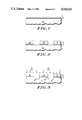
- FIGS. 1-4 illustrate, in cross-section, process steps wherein an isolating oxide is formed between device regions; and FIGS. 5-8 illustrate schematically, in crosssection, process steps in accordance with one embodiment of the invention wherein isolation is formed in a complementary substrate using a reduced number of masking steps.
- FIGS. 1-4 illustrate a preferred embodiment for achieving a locally enhanced oxide growth rate as one component of the necessary two region, differential growth rate requirement. Additionally, as illustrated, the preferred process for achieving the enhanced growth rate achieves this enhanced growth rate preferentially in the vertical direction compared to the lateral direction.
- FIGS. 1-4 localized oxide regions, recessed into the surface of a semiconductor substrate, are formed by a process in which the vertical growth rate is enhanced. Incorporation of this process into a process in accordance with the invention will be illustrated in the illustrative embodiment shown in FIGS. 5-8.
- the process illustrated in FIGS. 1-4 illustrates the formation of oxide isolation regions without the accompanying field doping.
- FIG.1 illustrates, in cross-section, a portion of a semiconductor substrate 10 in which it is desired to form a plurality of active regions which are isolated at the substrate surface by a localized oxide.
- an oxidation resistant layer of material Overlying the surface of substrate 10 is an oxidation resistant layer of material.
- the oxidation resistant layer includes a thin layer 12 of silicon dioxide and an overlying layer 14 of silicon nitride.
- the oxidation resistant material can be a layer of silicon nitride alone, various layers of oxide and nitride, silicon oxynitride, aluminum oxide, or the like.
- the process continues by patterning the oxidation resistant material to leave the material overlying the active device portions of the substrate.
- the patterning of the oxidation resistant material is accomplished by applying and photolithographically patterning a layer of photoresist to form photoresist regions 16 overlying what will become the active regions of the device to be formed.
- FIG. 2 shows three such regions, although the number, location, and shape of these regions will depend upon the device being fabricated.
- Patterned photoresist 16 is used in conventional manner to pattern the underlying layers of silicon nitride and silicon oxide.
- the patterning of the oxidation resistant material is done in conventional manner and is not critical to the practice of the invention.
- halogen ions and preferably chlorine ions, are implanted selectively into the surface of substrate 10 as illustrated in FIG. 3.
- the ions are selectively implanted into the substrate surface using the patterned oxidation resistant material 12,14 and preferably also the patterned photoresist 16 as an ion implantation mask.
- Implanted regions 18, which are doped with the halogen ions, are formed at the substrate surface in those locations where field oxide is to be formed.
- the implantation of ions, as illustrated by arrows 20, is an anisotropic process so that the location of the ions in the substrate is limited in lateral extent by the masking layers 12,14,16.
- lateral and vertical are referenced to the major surface 22 of substrate 10 and represent directions parallel and perpendicular thereto, respectively. Because of the anisotropic nature of the ion implantation process, implanted regions 18 are aligned with the openings in the implant mask with only minor extension (due to scattering and the like) of ions laterally underneath the masking layer.
- the exposed portions of substrate 10 are thermally oxidized to grow localized field oxide regions 24 as illustrated in FIG. 4.
- the nature of the oxidation process causes field oxide 24 to be partially recessed below the original surface 22.
- the localized implantation of halogen ions into the surface of substrate 10 causes the oxidation rate in the presence of those halogen ions to markedly increase over the oxidation rate in the absence of such halogen ions.
- An important result of the process of implanting halogen ions and then oxidizing is the increase in the oxidation rate in the vertical direction compared to the lateral direction. Conventional oxidation is an isotropic process.
- the oxidation process becomes anisotropic with the vertical growth rate in the direction illustrated by arrow 26 exceeding the lateral growth rate in the direction indicated by arrow 28.
- the anisotropic nature of the oxidation process apparently results from the localized implantation of the halogen ions; the oxidation rate is increased only in those regions which are doped with the halogen ions.
- the enhanced oxidation is also made selective. Different growth rates in implanted and unimplanted areas are thus realized.
- the oxidation of substrate 10 to form field oxide regions 24 causes the oxide to extend into the surface laterally as well as vertically.
- the lateral growth of oxide 24 causes the well known upward bending 30 of nitride layer 14 with the consequent formation of bird's beak 32.
- the lateral expansion of the field oxide and the formation of the bird's beak are deleterious because the lateral encroachment reduces the area of the active region, thus requiring an increase in the size of the integrated circuit chip.
- By increasing the vertical growth rate relative to the lateral growth rate a field oxide of the desired and necessary thickness is achieved with a reduced width and thus reduced encroachment into the active area.
- the increased oxidation rate also reduces the oxidation time required to achieve the necessary thickness and thus reduces the amount of time the device structure is exposed to a high temperature.
- FIGS. 5-8 illustrate, in cross-section, process steps in accordance with one embodiment of the invention, specifically for the fabrication and isolation of a CMOS device structure.
- the above-described oxide enhancement is combined with a dopant diffusion to provide an improved process for controlling the surface doping of at least two regions on a semiconductor surface, namely the field regions over the complementary N and P-type surface regions.
- FIG. 5 illustrates, in cross-section, a portion of a substrate 34 for the fabrication of a CMOS integrated circuit.
- the early processing steps have already been completed to fom complementary regions 36 and 38.
- Region 36 is of P-type conductivity and region 38 is of N-type conductivity.
- Overlying each of the complementary regions is a patterned layer of oxidation resistant material which, for purposes of illustration, includes an oxide layer 40 and an overlying layer of silicon nitride 42.
- the oxidation resistant material is patterned using a patterned photoresist 44.
- the surface of the substrate 34 is implanted with boron as illustrated by arrows 46.
- the boron implantation forms a shallow boron doped region 48,50 at the surface of the P-type and N-type regions 36,38 respectively.
- the boron will eventually provide an enhanced field threshold voltage for the portion of the substrate beneath the field oxide to be formed in the Ptype region 36.
- the boron is uniformly implanted into both N-type and P-type regions, however, so that this implantation can be done without an additional implantation mask.
- Photoresist layer 44 is removed after the boron implantation and an additional photoresist mask 52 is applied and patterned to mask P-type region 36.
- the unmasked portions of substrate 34 are implanted with halogen as illustrated by arrows 54 in FIG. 7 to form halogen doped regions 56 at the surface of N-type region 38.
- the energy of the halogen implant is selected so that the implant is masked by nitride 42 and oxide 40 as well as by photoresist mask 52.
- the halogen ions are thus implanted into what will become the field regions of the N-type region 38.
- field oxide regions 58,60 are thermally oxidizd to form field oxide regions 58,60 as illustrated in FIG. 8.
- Underlying field oxide 58 is an N-type region 2
- underlying field oxide region 60 is a P-type doped region 64. Because of the halogen implant and the enhanced oxidation rate which accompanies such an implant, field oxide region 58 is of greater thickness over N-type region 38 than is field oxide 60 formed over P-type region 36.
- dopants originally located in the semiconductor substrate such as boron and phosphorus, tend to segregate into the growing oxide or into the silicon substrate depending upon the segregation coeffients characteristic of those dopant materials.
- Boron for example, has a greater tendency to segregate into the growing thermal oxide and phosphorus has a tendency to segregate into or remain in the silicon substrate.
- the implanted boron from doped layer 50 is incorporated within field oxide 58.
- the differential oxidation range caused by the localized implantation of halogen ions thus results in an enhanced guard ring doping beneath the field oxides in both the N-type and P-type surface regions without the necessity for separate masking and implantation of P and N-type guard ring dopants.
- silicon substrates were implanted with halogen ions, specifically including chlorine ions and fluorine ions. Enhancement in the oxidation rate was found to be greatest with implantations of chlorine ions.
- the silicon samples were implanted with chlorine ions at implant energies between 20 kev and 160 kev. Doses ranged from 2.5 ⁇ 10 15 cm -2 to 1.0 ⁇ 10 16 cm -2 .
- some samples were implanted with multiple implants at a variety of energies to provide chlorine ions distributed with depth in the silicon wafer.
- the graded or multiple implants includes, for example, implants of: 1.0 ⁇ 10 16 cm -2 at 160 kev, 4.7 ⁇ 10 15 cm -2 at 65 kev, and 1.8 ⁇ 10 15 cm -2 at 20 kev or 5.0 ⁇ 10 15 cm -2 at 160 kev, 2.3 ⁇ 10 15 cm -2 at 65 kev, and 0.9 ⁇ 10 -15 cm -2 at 20 kev.
- Samples were subsequently oxidized at temperatures from about 830° C. to about 1000° C.
- the lower limit represents a temperature below which the oxidation rate was too low to be practical in a manufacturing environment.
- the upper limit is the highest temperature to which it was desired to subject the particular devices being fabricated. Oxidation in accordance with the invention can, of course, be carried out at temperatures either above or below the indicated range provided the temperature can be accommodated within the particular manufacturing process. Using the above indicated range of processing parameters, oxidation enhancements of as much as 95% were observed. The greatest enhancement in oxidation rate was found for the graded multiple implant with the oxidation being carried out for a short period of time at 1000° C.
- CMOS devices of the twin-well type were fabricated by oxidizing a silicon wafer to grow 30 nanometers of oxide on the surface.
- the wafers were selectively implanted through the oxide, with phosphorus at 100 kev to a dose of 5 ⁇ 10 12 cm -2 and with boron at 40 kev to a dose of 5 ⁇ 10 12 cm -2 to dope the N and P-type wells, respectively.
- the well implants were redistributed by annealing for four hours at 1200° C. to achieve a surface concentration of approximately 2 ⁇ 10 16 cm -3 .
- the active area of the devices was masked with an oxidation resistant barrier including a layer of thermal oxide overlaid with a layer of deposited silicon nitride.
- the wafers were divided into two groups, with one group receiving a boron implant of 1.0 ⁇ 10 13 cm -2 at 50 kev and with the other group receiving a boron implant of 2.0 ⁇ 10 13 cm -2 at 35 kev.
- the P-type well was then masked with photoresist and the N-type well received a chlorine implant consisting of two separate implants as follows: 5.0 ⁇ 10 15 cm -2 at 150 kev and 2.5 ⁇ 10 15 cm -2 at 65 kev.
- the wafers were then oxidized for 190 minutes at 1000° C. to form a thermal oxide of about 750 nanometers thickness on the unimplanted portion.
- the oxide on the chlorine implanted portion grew to a thickness of approximately 915 nanometers, representing an oxide enhancement of 22%.
- the fabrication of CMOS structures was then completed in normal fashion by steps including the growth of a gate oxide, deposition of polycrystalline silicon, deposition and patterning of contact metal, and the like.
- the structures were measured to determine the field threshold voltage in both the N and P-well regions.
- the field threshold was about -35 volts for both boron doping cycles.
- control devices which did not receive a chlorine implant had field thresholds of only -14.4 and -16.4 volts for the heavy and light boron implants, respectively.
- the field threshold voltage in the P-well region was measured to be 10.1 and 13.9 volts for the light and heavy boron implants respectively.
Abstract
Description
Claims (10)
Priority Applications (1)
| Application Number | Priority Date | Filing Date | Title |
|---|---|---|---|
| US07/053,917 US4743563A (en) | 1987-05-26 | 1987-05-26 | Process of controlling surface doping |
Applications Claiming Priority (1)
| Application Number | Priority Date | Filing Date | Title |
|---|---|---|---|
| US07/053,917 US4743563A (en) | 1987-05-26 | 1987-05-26 | Process of controlling surface doping |
Publications (1)
| Publication Number | Publication Date |
|---|---|
| US4743563A true US4743563A (en) | 1988-05-10 |
Family
ID=21987425
Family Applications (1)
| Application Number | Title | Priority Date | Filing Date |
|---|---|---|---|
| US07/053,917 Expired - Fee Related US4743563A (en) | 1987-05-26 | 1987-05-26 | Process of controlling surface doping |
Country Status (1)
| Country | Link |
|---|---|
| US (1) | US4743563A (en) |
Cited By (32)
| Publication number | Priority date | Publication date | Assignee | Title |
|---|---|---|---|---|
| US4839301A (en) * | 1988-12-19 | 1989-06-13 | Micron Technology, Inc. | Blanket CMOS channel stop implant employing a combination of n-channel and p-channel punch-through implants |
| US4847213A (en) * | 1988-09-12 | 1989-07-11 | Motorola, Inc. | Process for providing isolation between CMOS devices |
| US4920076A (en) * | 1988-04-15 | 1990-04-24 | The United States Of America As Represented By The United States Department Of Energy | Method for enhancing growth of SiO2 in Si by the implantation of germanium |
| US5308787A (en) * | 1993-10-22 | 1994-05-03 | United Microelectronics Corporation | Uniform field oxidation for locos isolation |
| US5338691A (en) * | 1990-05-31 | 1994-08-16 | Fuji Electric Co., Ltd. | Method of making a photodiode with reduced junction area |
| US5358894A (en) * | 1992-02-06 | 1994-10-25 | Micron Technology, Inc. | Oxidation enhancement in narrow masked field regions of a semiconductor wafer |
| US5369052A (en) * | 1993-12-06 | 1994-11-29 | Motorola, Inc. | Method of forming dual field oxide isolation |
| US5372951A (en) * | 1993-10-01 | 1994-12-13 | Advanced Micro Devices, Inc. | Method of making a semiconductor having selectively enhanced field oxide areas |
| US5576226A (en) * | 1994-04-21 | 1996-11-19 | Lg Semicon Co., Ltd. | Method of fabricating memory device using a halogen implant |
| US5614421A (en) * | 1994-03-11 | 1997-03-25 | United Microelectronics Corp. | Method of fabricating junction termination extension structure for high-voltage diode devices |
| US5643825A (en) * | 1994-12-29 | 1997-07-01 | Advanced Micro Devices, Inc. | Integrated circuit isolation process |
| US5698458A (en) * | 1994-09-30 | 1997-12-16 | United Microelectronics Corporation | Multiple well device and process of manufacture |
| US5869385A (en) * | 1995-12-08 | 1999-02-09 | Advanced Micro Devices, Inc. | Selectively oxidized field oxide region |
| US5918116A (en) * | 1994-11-30 | 1999-06-29 | Lucent Technologies Inc. | Process for forming gate oxides possessing different thicknesses on a semiconductor substrate |
| US6093659A (en) * | 1998-03-25 | 2000-07-25 | Texas Instruments Incorporated | Selective area halogen doping to achieve dual gate oxide thickness on a wafer |
| US6114257A (en) * | 1998-09-16 | 2000-09-05 | International Business Machines Corporation | Process for modified oxidation of a semiconductor substrate using chlorine plasma |
| US6127242A (en) * | 1994-02-10 | 2000-10-03 | Micron Technology, Inc. | Method for semiconductor device isolation using oxygen and nitrogen ion implantations to reduce lateral encroachment |
| US6171969B1 (en) * | 1998-03-13 | 2001-01-09 | Texas Instruments Incorporated | Uniform dopant distribution for mesas of semiconductors |
| US6228782B1 (en) * | 1999-05-11 | 2001-05-08 | Advanced Micro Devices, Inc. | Core field isolation for a NAND flash memory |
| US6335262B1 (en) | 1999-01-14 | 2002-01-01 | International Business Machines Corporation | Method for fabricating different gate oxide thicknesses within the same chip |
| US6358865B2 (en) * | 1999-05-14 | 2002-03-19 | Agere Systems Guardian Corp. | Oxidation of silicon using fluorine implant |
| US6383859B2 (en) * | 1998-12-28 | 2002-05-07 | Fujitsu Limited | Method of forming semiconductor device including patterning lower electrode of capacitor and gate electrode of transistor with same resist |
| US20030235964A1 (en) * | 2002-06-24 | 2003-12-25 | Micron Technology, Inc. | Reduction of field edge thinning in peripheral devices |
| US20040110429A1 (en) * | 2002-07-26 | 2004-06-10 | Eberhard Wizgall | Integrated intake manifold and heat exchanger |
| US6784115B1 (en) * | 1998-12-18 | 2004-08-31 | Mosel Vitelic, Inc. | Method of simultaneously implementing differential gate oxide thickness using fluorine bearing impurities |
| US6946344B2 (en) * | 2003-05-09 | 2005-09-20 | Nanya Technology Corporation | Method for forming trench capacitor |
| FR2870041A1 (en) * | 2004-05-06 | 2005-11-11 | Nanoraptor Sa | Fabrication of components with nanometric relief and/or variations in thickness, for micro-electro- mechanical systems, micro-motor and semiconductor applications |
| US20050287747A1 (en) * | 2004-06-29 | 2005-12-29 | International Business Machines Corporation | Doped nitride film, doped oxide film and other doped films |
| US20080128807A1 (en) * | 2005-01-12 | 2008-06-05 | Yasumori Fukushima | Semiconductor Device Fabrication Method And Semiconductor Device |
| CN101770986A (en) * | 2008-12-30 | 2010-07-07 | 联华电子股份有限公司 | Method for reducing gate leakage current and controlling threshold voltage shift and device |
| CN104701160A (en) * | 2013-12-10 | 2015-06-10 | 英飞凌科技股份有限公司 | Method of manufacturing a semiconductor structure and semiconductor structure |
| US20150279664A1 (en) * | 2014-04-01 | 2015-10-01 | Asia Pacific Microsystems, Inc. | Method for fabricating semiconductor devices having high-precision gaps |
Citations (7)
| Publication number | Priority date | Publication date | Assignee | Title |
|---|---|---|---|---|
| US3933530A (en) * | 1975-01-28 | 1976-01-20 | Rca Corporation | Method of radiation hardening and gettering semiconductor devices |
| US4013484A (en) * | 1976-02-25 | 1977-03-22 | Intel Corporation | High density CMOS process |
| US4027380A (en) * | 1974-06-03 | 1977-06-07 | Fairchild Camera And Instrument Corporation | Complementary insulated gate field effect transistor structure and process for fabricating the structure |
| US4133704A (en) * | 1977-01-17 | 1979-01-09 | General Motors Corporation | Method of forming diodes by amorphous implantations and concurrent annealing, monocrystalline reconversion and oxide passivation in <100> N-type silicon |
| US4144100A (en) * | 1977-12-02 | 1979-03-13 | General Motors Corporation | Method of low dose phoshorus implantation for oxide passivated diodes in <10> P-type silicon |
| US4466171A (en) * | 1980-04-29 | 1984-08-21 | U.S. Philips Corporation | Method of manufacturing a semiconductor device utilizing outdiffusion to convert an epitaxial layer |
| US4516316A (en) * | 1984-03-27 | 1985-05-14 | Advanced Micro Devices, Inc. | Method of making improved twin wells for CMOS devices by controlling spatial separation |
-
1987
- 1987-05-26 US US07/053,917 patent/US4743563A/en not_active Expired - Fee Related
Patent Citations (7)
| Publication number | Priority date | Publication date | Assignee | Title |
|---|---|---|---|---|
| US4027380A (en) * | 1974-06-03 | 1977-06-07 | Fairchild Camera And Instrument Corporation | Complementary insulated gate field effect transistor structure and process for fabricating the structure |
| US3933530A (en) * | 1975-01-28 | 1976-01-20 | Rca Corporation | Method of radiation hardening and gettering semiconductor devices |
| US4013484A (en) * | 1976-02-25 | 1977-03-22 | Intel Corporation | High density CMOS process |
| US4133704A (en) * | 1977-01-17 | 1979-01-09 | General Motors Corporation | Method of forming diodes by amorphous implantations and concurrent annealing, monocrystalline reconversion and oxide passivation in <100> N-type silicon |
| US4144100A (en) * | 1977-12-02 | 1979-03-13 | General Motors Corporation | Method of low dose phoshorus implantation for oxide passivated diodes in <10> P-type silicon |
| US4466171A (en) * | 1980-04-29 | 1984-08-21 | U.S. Philips Corporation | Method of manufacturing a semiconductor device utilizing outdiffusion to convert an epitaxial layer |
| US4516316A (en) * | 1984-03-27 | 1985-05-14 | Advanced Micro Devices, Inc. | Method of making improved twin wells for CMOS devices by controlling spatial separation |
Non-Patent Citations (12)
| Title |
|---|
| "Donor Generation in Monocrystalline Silicon by Halogen Implantation", Solid State Electronics, vol. 26, No. 3, pp. 241-246, 1983. |
| "Dopant Dependence of the Oxidation Rate of Ion Implanted Silicon Radiation Effects, vol. 47, pp. 203-210, 1980. |
| "Effect of Fluorine Implantation on the Kinetics of Dry Oxidation of Silicon", J. Appl. Phys. 60 (3), Aug. 1, 1986, pp. 985-990. |
| "Electrical Properties of MOS Devices Made with SILO Technology", IEDM 82, pp. 220-222. |
| "Kinetics of the Thermal Oxidation of Silicon in O2 /HCl Mixtures", J. Electrochem Soc. vol. 124, No. 5, May 1977, pp. 735-739. |
| "Selective Oxidation Technologies for High Density MOS", IEEE Electron Device Letters, EDL-2, No. 10, Oct. 1981, pp. 244-247. |
| Donor Generation in Monocrystalline Silicon by Halogen Implantation , Solid State Electronics, vol. 26, No. 3, pp. 241 246, 1983. * |
| Dopant Dependence of the Oxidation Rate of Ion Implanted Silicon Radiation Effects, vol. 47, pp. 203 210, 1980. * |
| Effect of Fluorine Implantation on the Kinetics of Dry Oxidation of Silicon , J. Appl. Phys. 60 (3), Aug. 1, 1986, pp. 985 990. * |
| Electrical Properties of MOS Devices Made with SILO Technology , IEDM 8 2 , pp. 220 222. * |
| Kinetics of the Thermal Oxidation of Silicon in O 2 /HCl Mixtures , J. Electrochem Soc. vol. 124, No. 5, May 1977, pp. 735 739. * |
| Selective Oxidation Technologies for High Density MOS , IEEE Electron Device Letters, EDL 2, No. 10, Oct. 1981, pp. 244 247. * |
Cited By (45)
| Publication number | Priority date | Publication date | Assignee | Title |
|---|---|---|---|---|
| US4920076A (en) * | 1988-04-15 | 1990-04-24 | The United States Of America As Represented By The United States Department Of Energy | Method for enhancing growth of SiO2 in Si by the implantation of germanium |
| US4847213A (en) * | 1988-09-12 | 1989-07-11 | Motorola, Inc. | Process for providing isolation between CMOS devices |
| US4839301A (en) * | 1988-12-19 | 1989-06-13 | Micron Technology, Inc. | Blanket CMOS channel stop implant employing a combination of n-channel and p-channel punch-through implants |
| US5338691A (en) * | 1990-05-31 | 1994-08-16 | Fuji Electric Co., Ltd. | Method of making a photodiode with reduced junction area |
| US5358894A (en) * | 1992-02-06 | 1994-10-25 | Micron Technology, Inc. | Oxidation enhancement in narrow masked field regions of a semiconductor wafer |
| US5661335A (en) * | 1993-10-01 | 1997-08-26 | Advanced Micro Devices, Inc. | Semicondutor having selectively enhanced field oxide areas and method for producing same |
| US5372951A (en) * | 1993-10-01 | 1994-12-13 | Advanced Micro Devices, Inc. | Method of making a semiconductor having selectively enhanced field oxide areas |
| US5308787A (en) * | 1993-10-22 | 1994-05-03 | United Microelectronics Corporation | Uniform field oxidation for locos isolation |
| US5369052A (en) * | 1993-12-06 | 1994-11-29 | Motorola, Inc. | Method of forming dual field oxide isolation |
| US6127242A (en) * | 1994-02-10 | 2000-10-03 | Micron Technology, Inc. | Method for semiconductor device isolation using oxygen and nitrogen ion implantations to reduce lateral encroachment |
| US5614421A (en) * | 1994-03-11 | 1997-03-25 | United Microelectronics Corp. | Method of fabricating junction termination extension structure for high-voltage diode devices |
| US5576226A (en) * | 1994-04-21 | 1996-11-19 | Lg Semicon Co., Ltd. | Method of fabricating memory device using a halogen implant |
| US5698458A (en) * | 1994-09-30 | 1997-12-16 | United Microelectronics Corporation | Multiple well device and process of manufacture |
| US5918116A (en) * | 1994-11-30 | 1999-06-29 | Lucent Technologies Inc. | Process for forming gate oxides possessing different thicknesses on a semiconductor substrate |
| US5643825A (en) * | 1994-12-29 | 1997-07-01 | Advanced Micro Devices, Inc. | Integrated circuit isolation process |
| US5869385A (en) * | 1995-12-08 | 1999-02-09 | Advanced Micro Devices, Inc. | Selectively oxidized field oxide region |
| US6171969B1 (en) * | 1998-03-13 | 2001-01-09 | Texas Instruments Incorporated | Uniform dopant distribution for mesas of semiconductors |
| US6093659A (en) * | 1998-03-25 | 2000-07-25 | Texas Instruments Incorporated | Selective area halogen doping to achieve dual gate oxide thickness on a wafer |
| US6114257A (en) * | 1998-09-16 | 2000-09-05 | International Business Machines Corporation | Process for modified oxidation of a semiconductor substrate using chlorine plasma |
| KR100341198B1 (en) * | 1998-09-16 | 2002-06-20 | 포만 제프리 엘 | Process for modified oxidation of a semiconductor substrate using chlorine plasma |
| US6784115B1 (en) * | 1998-12-18 | 2004-08-31 | Mosel Vitelic, Inc. | Method of simultaneously implementing differential gate oxide thickness using fluorine bearing impurities |
| US6383859B2 (en) * | 1998-12-28 | 2002-05-07 | Fujitsu Limited | Method of forming semiconductor device including patterning lower electrode of capacitor and gate electrode of transistor with same resist |
| US6335262B1 (en) | 1999-01-14 | 2002-01-01 | International Business Machines Corporation | Method for fabricating different gate oxide thicknesses within the same chip |
| US6228782B1 (en) * | 1999-05-11 | 2001-05-08 | Advanced Micro Devices, Inc. | Core field isolation for a NAND flash memory |
| US6358865B2 (en) * | 1999-05-14 | 2002-03-19 | Agere Systems Guardian Corp. | Oxidation of silicon using fluorine implant |
| US7262102B2 (en) * | 2002-06-24 | 2007-08-28 | Micron Technology, Inc. | Reduction of field edge thinning in peripheral devices |
| US20030235964A1 (en) * | 2002-06-24 | 2003-12-25 | Micron Technology, Inc. | Reduction of field edge thinning in peripheral devices |
| US7563679B2 (en) | 2002-06-24 | 2009-07-21 | Micron Technology, Inc. | Reduction of field edge thinning in peripheral devices |
| US20070264784A1 (en) * | 2002-06-24 | 2007-11-15 | Micron Technology, Inc. | Reduction of field edge thinning in peripheral devices |
| US20060019449A1 (en) * | 2002-06-24 | 2006-01-26 | Micron Technology, Inc. | Reduction of field edge thinning in peripheral devices |
| US7241662B2 (en) * | 2002-06-24 | 2007-07-10 | Micron Technology, Inc. | Reduction of field edge thinning in peripheral devices |
| US20040110429A1 (en) * | 2002-07-26 | 2004-06-10 | Eberhard Wizgall | Integrated intake manifold and heat exchanger |
| US6946344B2 (en) * | 2003-05-09 | 2005-09-20 | Nanya Technology Corporation | Method for forming trench capacitor |
| FR2870041A1 (en) * | 2004-05-06 | 2005-11-11 | Nanoraptor Sa | Fabrication of components with nanometric relief and/or variations in thickness, for micro-electro- mechanical systems, micro-motor and semiconductor applications |
| US20050287747A1 (en) * | 2004-06-29 | 2005-12-29 | International Business Machines Corporation | Doped nitride film, doped oxide film and other doped films |
| US20080054228A1 (en) * | 2004-06-29 | 2008-03-06 | Chakravarti Ashima B | Doped nitride film, doped oxide film and other doped films |
| US7595010B2 (en) | 2004-06-29 | 2009-09-29 | International Business Machines Corporation | Method for producing a doped nitride film, doped oxide film and other doped films |
| US20080128807A1 (en) * | 2005-01-12 | 2008-06-05 | Yasumori Fukushima | Semiconductor Device Fabrication Method And Semiconductor Device |
| US7829400B2 (en) * | 2005-01-12 | 2010-11-09 | Sharp Kabushiki Kaisha | Semiconductor device fabrication method and semiconductor device |
| CN101770986A (en) * | 2008-12-30 | 2010-07-07 | 联华电子股份有限公司 | Method for reducing gate leakage current and controlling threshold voltage shift and device |
| CN101770986B (en) * | 2008-12-30 | 2014-03-12 | 联华电子股份有限公司 | Method for reducing gate leakage current and controlling threshold voltage shift and device |
| CN104701160A (en) * | 2013-12-10 | 2015-06-10 | 英飞凌科技股份有限公司 | Method of manufacturing a semiconductor structure and semiconductor structure |
| CN104701160B (en) * | 2013-12-10 | 2018-04-13 | 英飞凌科技股份有限公司 | Manufacture the method and semiconductor structure of semiconductor structure |
| US20150279664A1 (en) * | 2014-04-01 | 2015-10-01 | Asia Pacific Microsystems, Inc. | Method for fabricating semiconductor devices having high-precision gaps |
| CN104973566A (en) * | 2014-04-01 | 2015-10-14 | 亚太优势微系统股份有限公司 | Micro-electro-mechanical wafer structure with precise gap and manufacturing method thereof |
Similar Documents
| Publication | Publication Date | Title |
|---|---|---|
| US4743563A (en) | Process of controlling surface doping | |
| US4748134A (en) | Isolation process for semiconductor devices | |
| US4516316A (en) | Method of making improved twin wells for CMOS devices by controlling spatial separation | |
| US4717683A (en) | CMOS process | |
| CA1257710A (en) | Method for the manufacture of lsi complementary mos field effect transistor circuits | |
| US4382827A (en) | Silicon nitride S/D ion implant mask in CMOS device fabrication | |
| US5219784A (en) | Spacer formation in a bicmos device | |
| EP0051488B1 (en) | Method for manufacturing a semiconductor device | |
| US4554726A (en) | CMOS Integrated circuit technology utilizing dual implantation of slow and fast diffusing donor ions to form the n-well | |
| US4357622A (en) | Complementary transistor structure | |
| US4574467A (en) | N- well CMOS process on a P substrate with double field guard rings and a PMOS buried channel | |
| US5091332A (en) | Semiconductor field oxidation process | |
| US4711017A (en) | Formation of buried diffusion devices | |
| US5795801A (en) | MethodS of fabricating profiled device wells for improved device isolation | |
| KR0133540B1 (en) | Bicmos process for forming shallow npn emitters and mosfet | |
| EP0405045A1 (en) | A mixed technology integrated circuit comprising CMOS structures and efficient lateral bipolar transistors with a high early voltage and fabrication thereof | |
| WO1995008843A1 (en) | Latid implants for increasing the effective width of transistor elements in a semiconductor device | |
| US5047357A (en) | Method for forming emitters in a BiCMOS process | |
| US4797372A (en) | Method of making a merge bipolar and complementary metal oxide semiconductor transistor device | |
| US4373252A (en) | Method for manufacturing a semiconductor structure having reduced lateral spacing between buried regions | |
| EP0144823A2 (en) | Method of fabricating a lateral PNP transistor | |
| EP0150582B1 (en) | Silicon gigabits per second metal-oxide-semiconductor device processing | |
| US4485552A (en) | Complementary transistor structure and method for manufacture | |
| US6943413B2 (en) | BI-CMOS integrated circuit | |
| US4535529A (en) | Method of making semiconductor devices by forming an impurity adjusted epitaxial layer over out diffused buried layers having different lateral conductivity types |
Legal Events
| Date | Code | Title | Description |
|---|---|---|---|
| AS | Assignment |
Owner name: MOTOROLA, INC., A CORP. OF DE.,ILLINOIS Free format text: ASSIGNMENT OF ASSIGNORS INTEREST;ASSIGNORS:PFIESTER, JAMES R.;ALVIS, JOHN R.;HOLLAND, ORIN W.;SIGNING DATES FROM 19870509 TO 19870522;REEL/FRAME:004730/0750 Owner name: MOTOROLA, INC., SCHAUMBURG, ILLINOIS, A CORP. OF D Free format text: ASSIGNMENT OF ASSIGNORS INTEREST.;ASSIGNORS:PFIESTER, JAMES R.;ALVIS, JOHN R.;HOLLAND, ORIN W.;REEL/FRAME:004730/0750;SIGNING DATES FROM 19870509 TO 19870522 |
|
| FEPP | Fee payment procedure |
Free format text: PAYOR NUMBER ASSIGNED (ORIGINAL EVENT CODE: ASPN); ENTITY STATUS OF PATENT OWNER: LARGE ENTITY |
|
| FPAY | Fee payment |
Year of fee payment: 4 |
|
| FPAY | Fee payment |
Year of fee payment: 8 |
|
| REMI | Maintenance fee reminder mailed | ||
| LAPS | Lapse for failure to pay maintenance fees | ||
| FP | Lapsed due to failure to pay maintenance fee |
Effective date: 20000510 |
|
| STCH | Information on status: patent discontinuation |
Free format text: PATENT EXPIRED DUE TO NONPAYMENT OF MAINTENANCE FEES UNDER 37 CFR 1.362 |